

Page 1
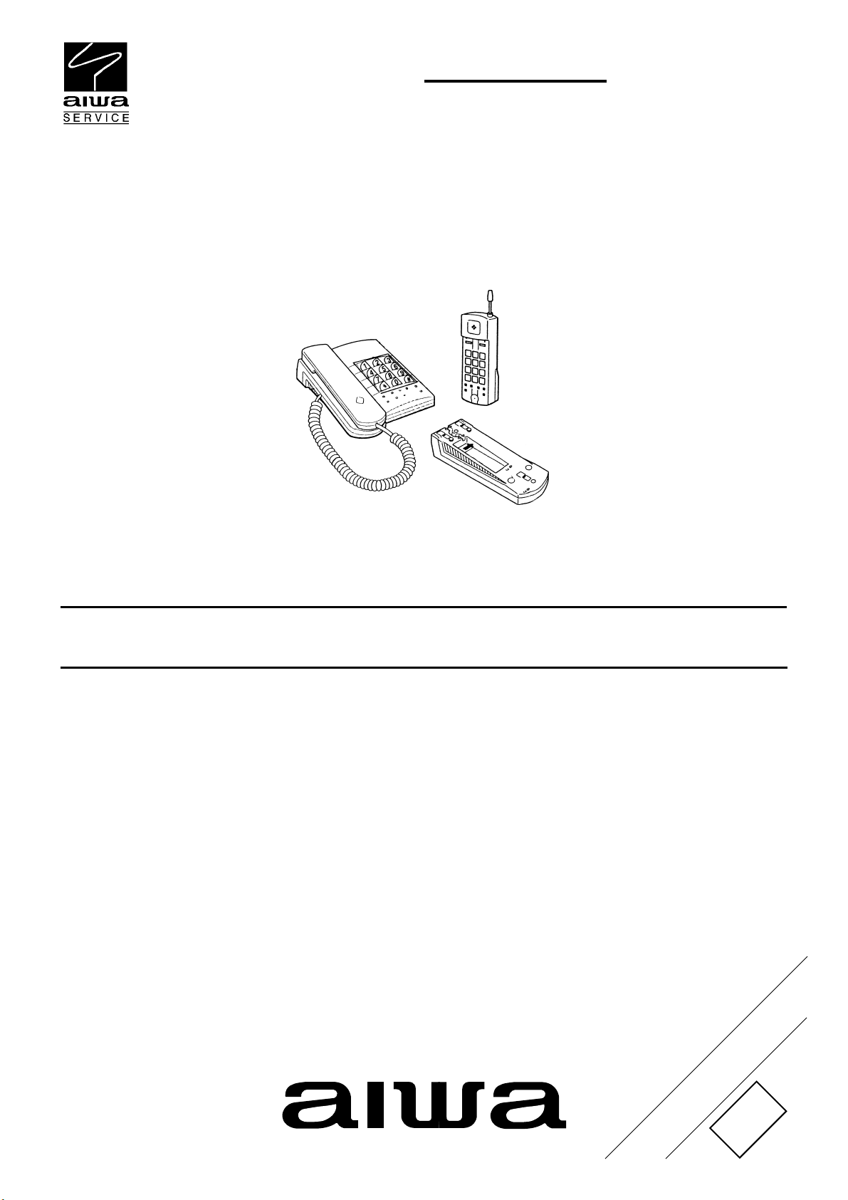
TN-F205
AEZ
SERVICE MANUAL
CORDLESS TELEPHONE
MODEL CODE : 86HR8-0117(B)
86HR8-1111(W)
86HR8-4444(L)
86HR8-8888(ST)
This Service Manual is the "Revision Publishing" and replaces "Simple Manual"
(S/M Code No. 09-99A-335-8T1).
S/M Code No. 09-99A-335-8R1
REVISION
DATA
Page 2
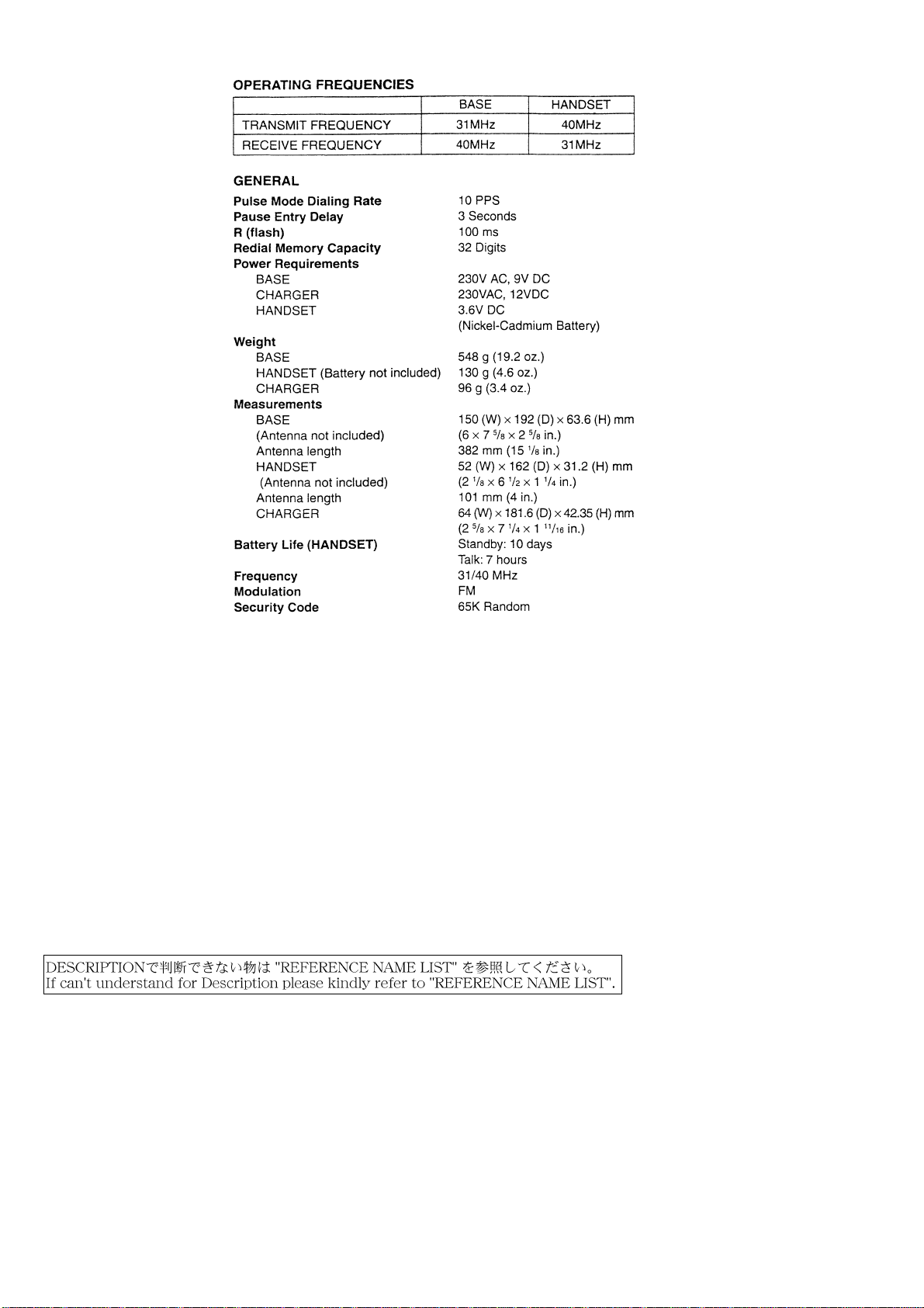
SPECIFICATIONS
Design and specifications are subject to change without
•
notice
.
ACCESSORIES/PACKAGE LIST
REF. NO PART NO. KANRI DESCRIPTION
!
1 S0-112-290-000 APA-EI35EN 230V 12VDC
!
2 S0-109-090-000 APA-EI35EN 230V 9VDC
3 S8-PCD-910-820 INSTRUCTION BOOK(TN-F205AEZ1-E
3 S8-PCD-910-920 INSTRUCTION BOOK(TN-F205AEZ1-S
4 S4-360-070-000 BATT IN-CD 3.6V
NO.
2
Page 3
E C B E B C
B
E
C
2SC2714
KTC3195
KSP42
KSP43
KSP92
2SA1037
KTC3880
MMBT3904
SST3906
ELECTRICAL MAIN PARTS LIST
REF. NO PART NO. KANRI DESCRIPTION
IC
88-PCD-605-010 IC,TB31224F
S8-331-000-000 IC,TA31002P/H31002P/HA31002P
S0-106-201-034 IC,TEA1062
S2-309-024-040 IC,LTV817
S0-391-340-010 IC,W91340N
87-A21-136-040 IC,AT24C01A-10SC 8P
87-A20-751-010 IC,L7805CV
S9-570-290-000 IC,KIA7029F
TRANSISTOR
SA-039-040-000 C-TR,MMBT3904
S3-146-319-525 TR,KTC3195Y
S8-009-200-010 TR,KSP92
S8-004-200-000 TR,KSP42
89-327-143-010 C-TR,2SC2714Y
S8-004-300-000 TR,KSP43
SA-039-060-010 TR,SST3906
SA-010-372-000 TR,2SA1037AKQ
SA-038-800-250 TR,KTC3880Y
DIODE
87-A40-226-080 DIODE,SVC251SPA
87-017-781-080 RECTIFIER IN-4004
S0-102-701-220 ZENER,27V 1/2W BZX55-C27 SEMTE
S0-100-821-240 ZENER,8.2V 1/2W BZX55-C8V2 SEM
87-A40-587-080 ZENER,BZX55-C5V1 5.1V
82-135-799-010 DIODE,IN4148
S0-100-331-220 ZENER,3.3V 1/2W BZX55-C3V3 SEM
S0-100-561-230 ZENER,BZX55-C5V6 5.6V
S0-100-621-210 ZENER,BZX55-C6V2 6.2V
MAIN C.B
C47 S0-471-100-3K0 CAP,CER 470PF-3000V
C65 87-010-545-010 CAP,E 0.22-50V
C76 87-010-546-080 CAP,E 0.33-50V
C106 87-010-546-080 CAP,E 0.33-50V
C118 S1-474-112-500 CAP,M 0.47-250V
C132 87-010-053-810 CAP,E 1-50V
C142 S0-471-115-000 CAP,CER 470PF-/500
C143 S0-471-115-000 CAP,CER 470PF-/500
CON2 S2-101-302-000 CONN,21P 2.0MM
DX1 S3-001-640-000 DUPLEXER 31/40MHZ
IFT1 S0-039-300-070 IFT KY393N
IFT2 S0-075-600-070 IFT,7MM 455KHZ
IFT3 S0-008-450-070 IFT,KY845R
IFT4 S0-039-200-070 IFT KY392N
IFT5 S0-039-400-070 IFT KY394N
J2 S0-022-020-000 JACK,TEL MINI L/P 6P2C
J3 S1-004-700-040 POWER JACK DC HEC0470-01-250
L1 87-003-133-010 INDUCTOR,0.22UH
L2 87-005-166-010 INDUCTOR,1.2UH
L3 87-005-189-080 INDUCTOR,2.7UH
L4 8Z-PC6-636-080 INDUCTOR,2.2UH
L6 87-003-139-080 INDUCTOR,0.56UH
L7 87-005-696-080 COIL,100UH
L9 87-005-696-080 COIL,100UH
L10 87-003-097-010 COIL,1UH
L11 87-003-097-010 COIL,1UH
L12 87-003-097-010 COIL,1UH
L13 87-003-097-010 COIL,1UH
L14 87-005-696-080 COIL,100UH
L15 87-005-696-080 COIL,100UH
L16 87-005-696-080 COIL,100UH
R40 S0-222-500-120 RES,2.2K-1/2W
SW1 S2-201-220-000 SW,HOOK 2P2T
SW2 S2-200-000-040 SW,SLIDE 2P2T
NO.
REF. NO PART NO. KANRI DESCRIPTION
NO.
SW3 S1-300-001-000 SW,SLIDE 1P3T
T1 S0-004-500-180 CER,FILTER LTW33-450E
VAR1 S3-300-700-000 VARISTOR SAS-331KD07 330V
VR1 S1-030-850-000 SFR,10K
VR3 S1-030-850-000 SFR,10K
X1 S6-111-504-000 X’TAL,11.15MHz HC49/U
X2 S0-001-070-010 CER,FILTER
X3 S6-003-580-010 CER,RESO CSA3.58MG
KEY C.B
LED5 87-070-106-010 LED,SE3001 RED
LED6 87-070-106-010 LED,SE3001 RED
LED7 87-070-106-010 LED,SE3001 RED
HS-RF C.B
C12 87-010-075-040 CAP,E 10-16V
C15 87-010-380-010 CAP,E 47-16V
C16 87-015-696-080 CAP,E 2.2-50V
C19 87-010-545-010 CAP,E 0.22-50V
C24 87-010-075-040 CAP,E 10-16V
C30 87-015-696-080 CAP,E 2.2-50V
C33 87-010-380-010 CAP,E 47-16V
C65 87-010-400-010 CAP,E 0.47-50V
C85 87-010-380-010 CAP,E 47-16V
C87 87-010-264-040 CAP,E 100-10V
DX1 S3-001-650-000 DUPLEXER 31/40MHZ
IFT1 S0-002-860-070 IFT,KL286N
IFT2 S0-075-600-070 IFT,7MM 455KHZ
IFT3 S0-002-760-070 IFT,KL276N
IFT4 S0-002-741-070 IFT,KL274N
IFT5 S0-002-770-070 IFT,KL277N
J1 S0-200-2P1-500 HEADER KINDTECH 15P
L1 87-003-106-010 INDUCTOR,0.33UH
L2 87-005-166-010 INDUCTOR,1.2UH
L3 87-005-674-080 INDUCTOR,1.5UH
L4 S0-100-152-010 INDUCTOR,10UH
L5 87-003-133-010 INDUCTOR,0.22UH
T1 S0-004-500-180 CER,FILTER LTW33-450E
VR1 S1-030-850-000 SFR,10K
VR3 S1-030-850-000 SFR,10K
X1 S6-111-501-000 X’TAL,11.15MHZ
X2 S0-001-070-010 CER,FILTER
X3 S3-327-681-000 X’TAL,32.768KHZ
HAND KEY C.B
B1 SB-2BE-HA0-200 HEADER JST 2PIN
L1 87-003-150-080 INDUCTOR 68UH
L2 87-003-150-080 INDUCTOR 68UH
LED1 S0-321-610-010 C-LED,3.2-1.6(RED)
LED2 S0-321-610-010 C-LED,3.2-1.6(RED)
LED3 S0-049-410-030 LED,3MM(GRN)
LED4 S0-049-410-030 LED,3MM(GRN)
LED5 S0-049-410-030 LED,3MM(GRN)
LED6 S0-049-410-030 LED,3MM(GRN)
LED C.B
LED901 87-070-106-010 LED,SE3001 RED
CHG C.B
J901 S1-004-700-020 JACK,POWER DC470/MSC
R902 S0-271-500-010 RES,270-1W
BU-SP C.B
• Regarding connectors, they are not stocked as they are not the initial order items.
The connectors are available after they are supplied from connector manufacturers upon the order is received.
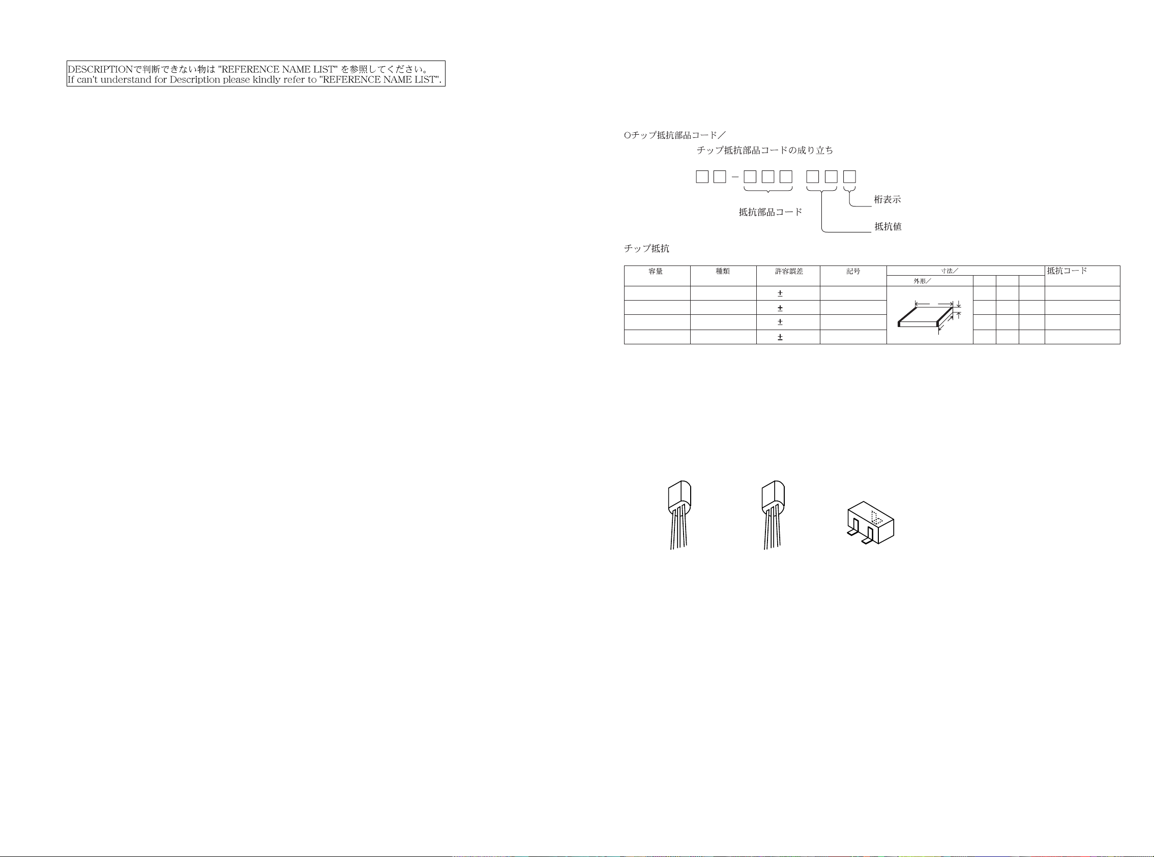
CHIP RESISTOR PART CODE
Chip Resistor Part Coding
88
A
Resistor Code
Chip resistor
Wattage Type Tolerance
1/16W 1005 5% CJ
1/16W
1/10W
1/8W
1608
2125
3216
5%
5%
5%
TRANSISTOR ILLUSTRATION
Symbol
Figure
Value of resistor
CJ
CJ
CJ
43
Form
L
W
Dimensions (mm)
LW t
1.0 0.5 0.35 104
t
1.6 0.8 0.45
2 1.25 0.45
1.6
0.55
3.2
Resistor Code
108
118
128
: A
: A
Page 4
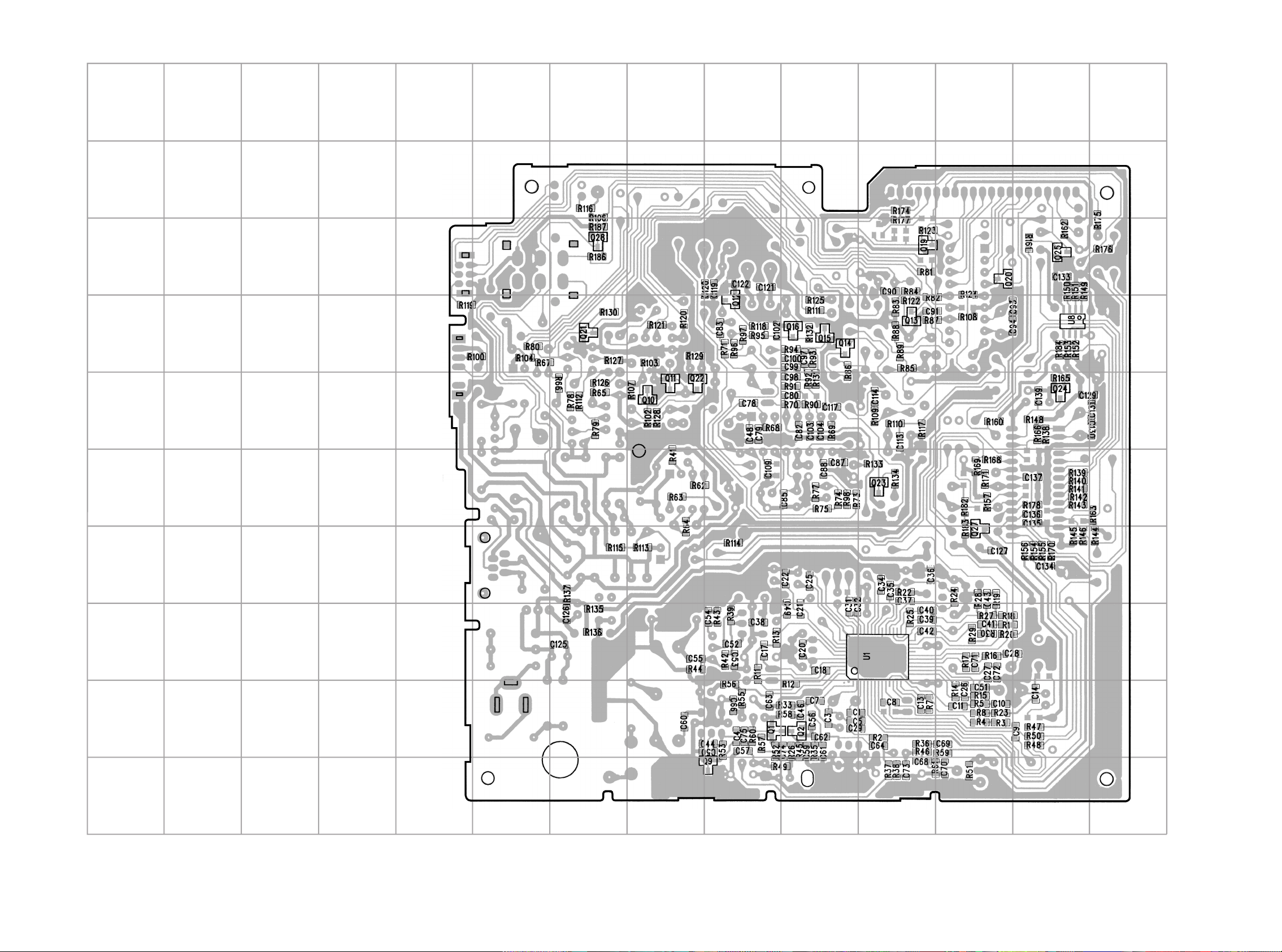
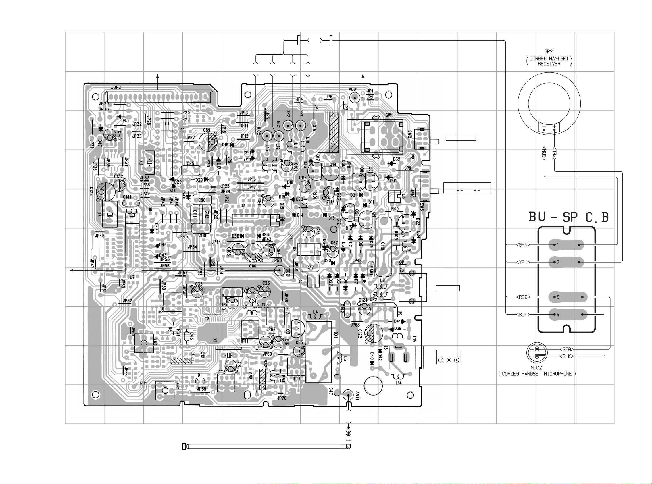
WIRING-1 (BU MAIN)
14
13 12 11 10 9 8
MAIN C.B
(CHIP PARTS)
7
6
5
432
1
A
B
C
D
38
39
48
114
25
15
24
E
F
G
H
I
J
65
Page 5
1
234567
BLK
8
9
10
11 12 13
14
A
MAIN C.B
(INSERTED PARTS)
TO/FROM KEY C.B
CON1
BLK
RED
YEL
GRN
TO/FROM MAIN C.B
VDD2
B
1
C
D
E
51015 2120
1
18
109
1
28
8
142
3
1
SW1
(HOOK)
SW2
TONE/PULSE
SW3
RINGER
HIGH LOW OFF
F
VDD1
G
TO/FROM MAIN C.B
H
I
14 15
916
4
58
3
4
1
2
1
J2
TEL. LINE
J3
DC 9V
J
RED
ANT1 (BASE UNIT ANTENNA)
87
Page 6
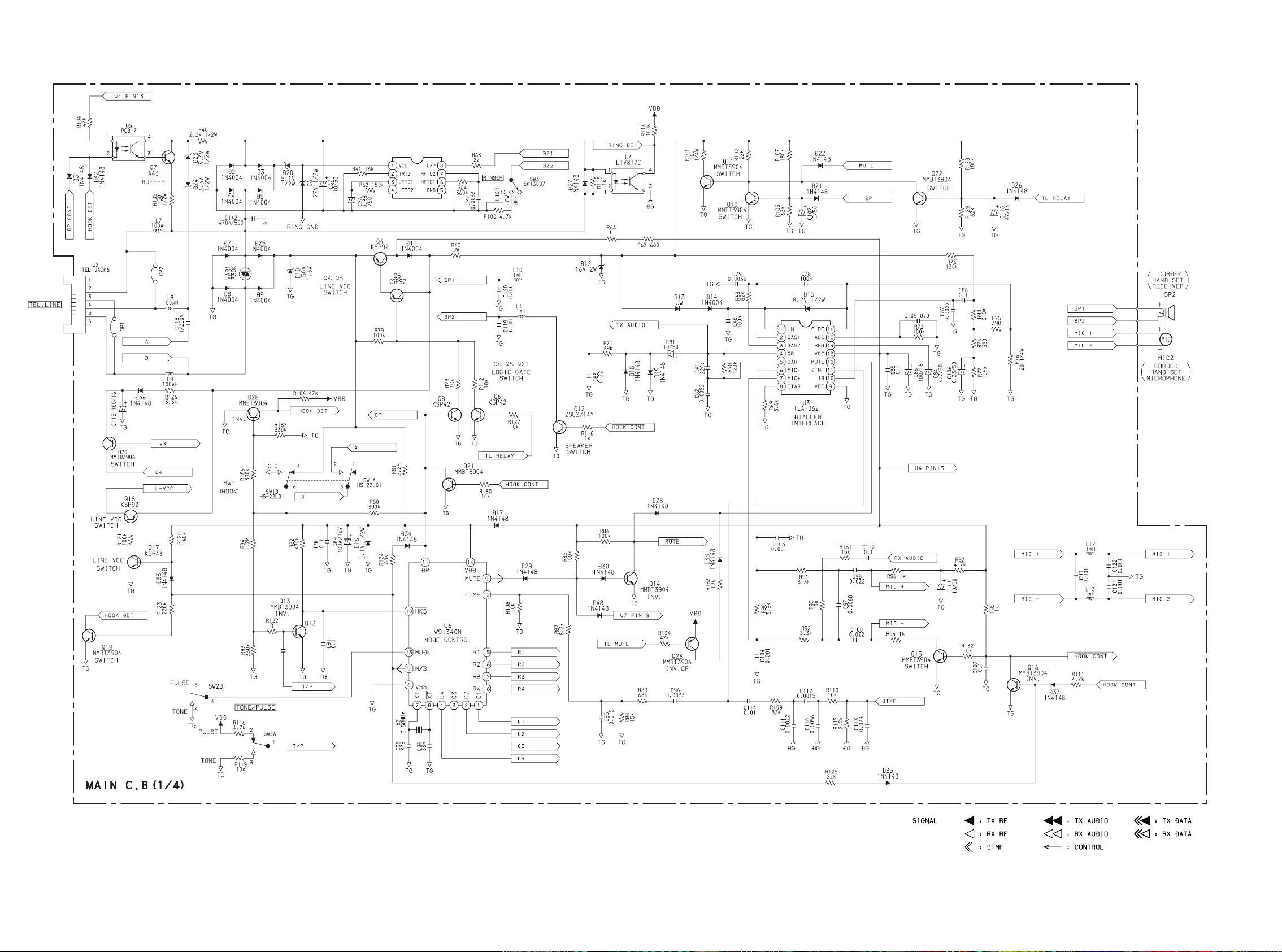
SCHEMATIC DIAGRAM-1 (MAIN 1/4)
TA31002P/H31002P/HA31002P
U2
C998
2200p
109
Page 7
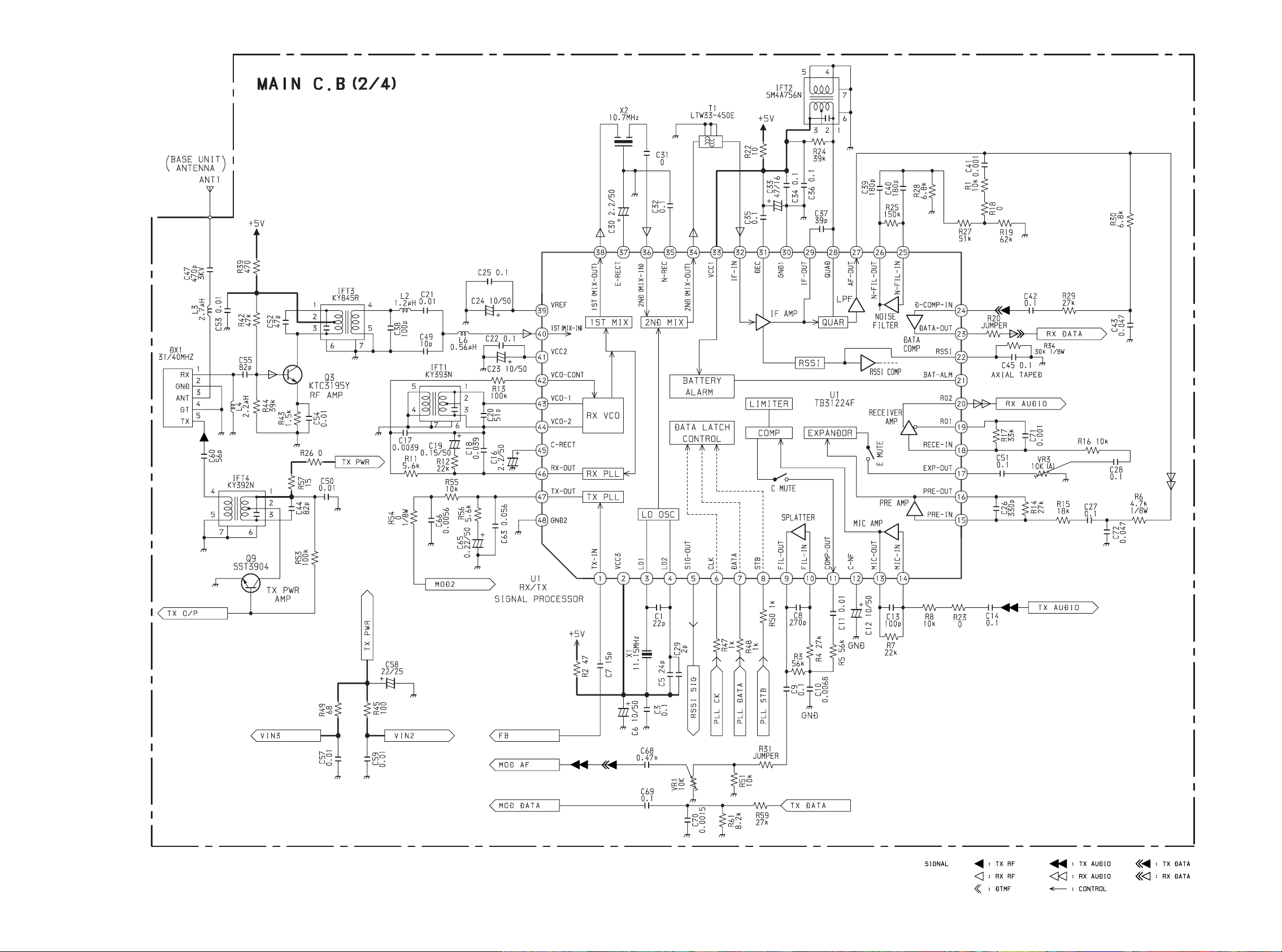
SCHEMATIC DIAGRAM-2 (MAIN 2/4)
1211
Page 8
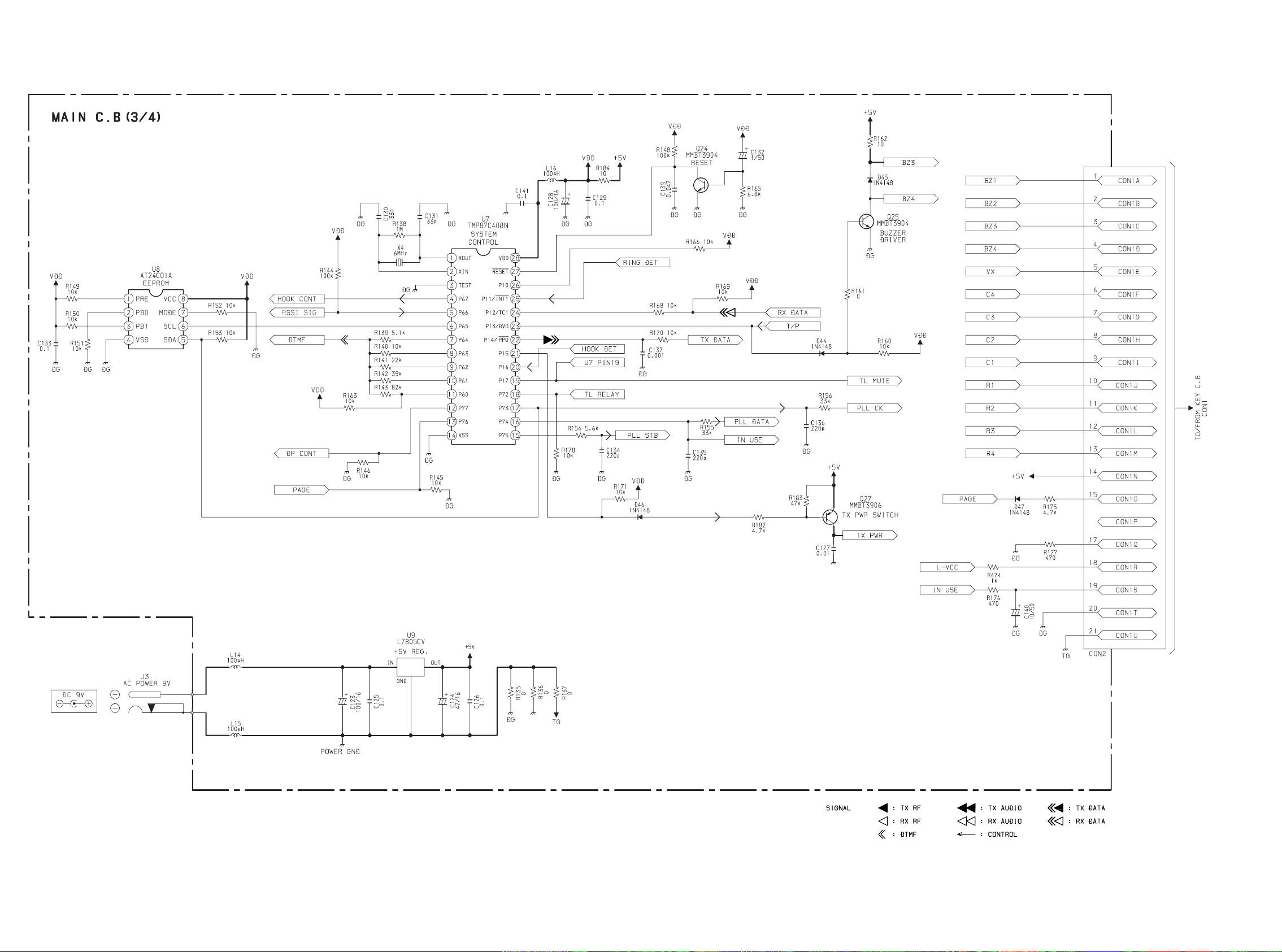
SCHEMATIC DIAGRAM-3 (MAIN 3/4)
1413
Page 9
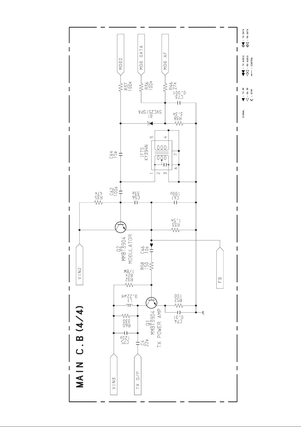
SCHEMATIC DIAGRAM-4 (MAIN 4/4)
15
Page 10
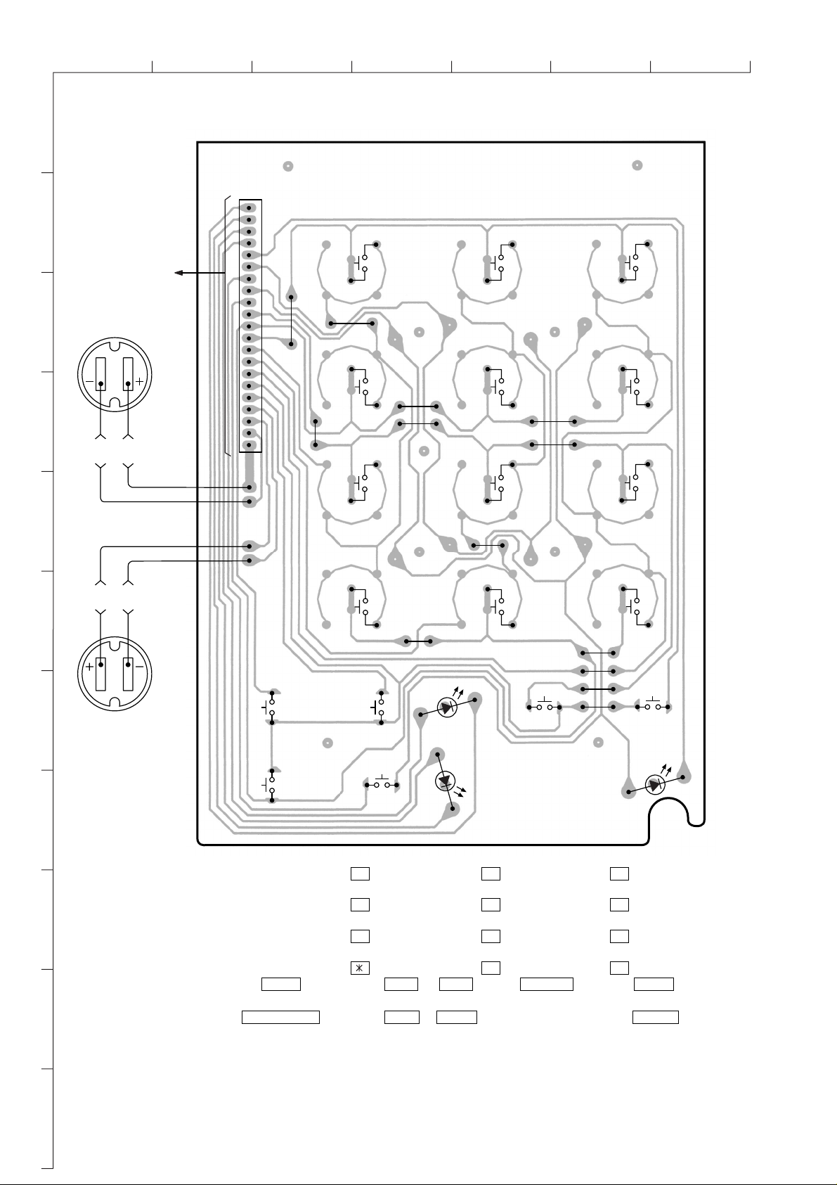
WIRING-2 (KEY)
1
234567
A
B
C
BZ2
D
BLK
RED
E
C0N2
TO/FROM MAIN C.B
KEY C.B
CON1
121
SW1
SW4
SW7
SW2
SW5
SW8
SW3
SW6
SW9
RED
BLK
F
G
BZ3
H
I
J
SW14
SW16
SW14
FLASH
SW16
REDIAL/PAUSE
SW10
SW1
1
SW4
4
SW7
7
SW10
SW17
SW18
SW17
HOLD
SW18
PAGE
LED7
LED7
HOLD
LED5
IN-USE
LED5
SW11
SW2
2
SW5
5
SW8
8
SW11
0
SW15
SW15
MEMORY
SW12
SW3
3
SW6
6
SW9
9
SW12
#
SW13
LED6
SW13
STORE
LED6
POWER
K
16
Page 11
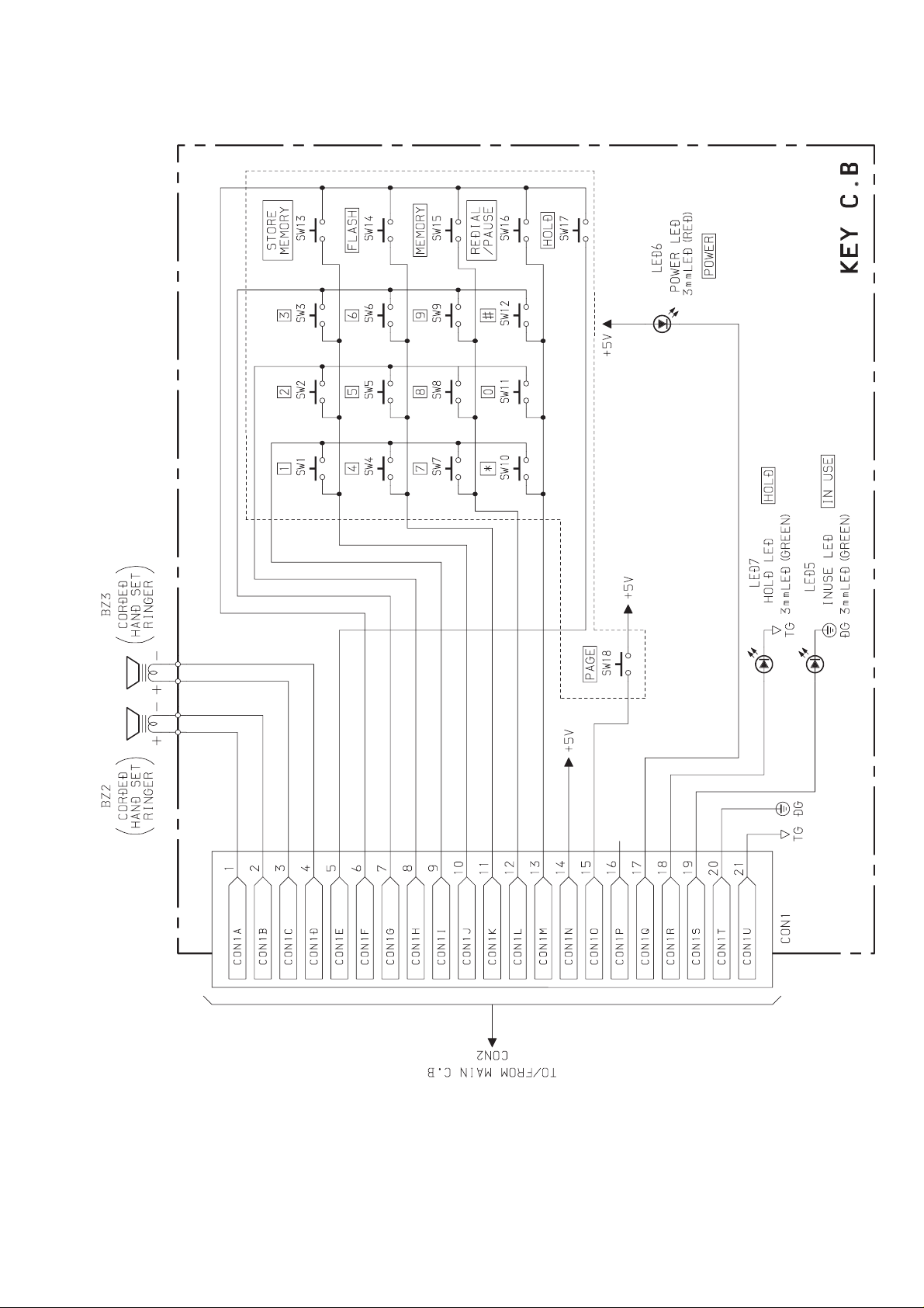
SCHEMATIC DIAGRAM-5 (KEY)
17
Page 12

WIRING-3 (HAND KEY)
1
A
234567
HAND-KEY C.B
TO/FROM HS-RF C.B
CON1
B
C
D
E
R13
SW15
LED2
CON1
R8
R7
R12
R1
R5R4R3
R2
R15
R14
SW18SW17
LED4 LED3
R9
115
R6
E
D5
LED1
SW19
C
SW1
Q1
R10
R11
B
LED2
TALK
SW15
TALK
SW17
1
LED1
BATT. LOW
SW1
MEMORY
SW18
2
SW19
3
F
G
H
I
Nickel-Cadmium Battery
J
RED
3.6V DC
BLK
SW14SW13SW12
SW7 SW8 SW9
LED5 LED6
SW4SW3SW2
1
1
2
2
B1
SW11
SW10
SW6 SW16
C5
D3
D2
C1
L2
SW5
D4
C4
ZD2
CHG1CHG2
D1
ZD1
SW20
C2
L1
SW12
4
SW7
7
LED3,4,5,6
(KEY BACK LIGHT)
SW2
SW11
R/P
SW6
FLASH
SW10
VOL
SW13
5
SW8
8
SW3
0
SW5
STORE
SW14
6
SW9
9
SW4
#
SW16
CH
SW9
PASE INT
K
TO/FROM LED C.B
18
Page 13

SCHEMATIC DIAGRAM-6 (HAND KEY)
3MM
3MM
3MM
3MM
LED
DRIVER
3.2-1.6
3.2-1.6
Ni-cd
BATTERY
3.6V
TO/FROM LED C.B
19
Page 14

WIRING-4 (HS-RF: COMPONENT)
7
6
5
HS-RF C.B
1
8
45
432
(COMPONENT SIDE)
33
34
44
1
11 12
23
22
1
A
B
C
D
25
38
39 48
DX1
BLK
1524
14
1
RED
M1
HANDSET
MICROPHONE
E
F
G
H
I
L5 L3
20
J
Page 15

WIRING-5 (HS-RF: CONDUCTOR)
WIRING-6 (CHG/LED)
1
234567
1
A
B
C
D
RED
BLK
2
HS-RF C.B
HANDSET
ANTENNA
3
456
(CONDUCTOR SIDE)
TO/FROM
HAND KEY C.B
115
RED
13
BLK
7
A
B
C
J901
D
BZ1
(HANDSET RINGER)
E
F
G
H
I
SP1
HANDSET
RECIVER
E
F
G
H
I
R902
R901
TO/FROM HAND KEY C.B
J
J
K
2221
Page 16

SCHEMATIC DIAGRAM-7 (HS-RF 1/3)
1
5
10
OSC
SWITCH
15
2423
Page 17

SCHEMATIC DIAGRAM-8 (HS-RF 2/3)
2625
Page 18

SCHEMATIC DIAGRAM-9 (HS-RF 3/3)
IC BLOCK DIAGRAM
IC, AT24C01A-10SC
IC, TA31002P/H31002P/HA31002P
IC, TEA1062
R 1
LOW
3 4
+
C 1
-
OSC
1
5
f
POWER
(WITH
HYSTERESIS)
C 2
SUPPLY
2
R 2
7
HIGH
OSC
+
6 8
f
-
Note: R1, R2, C1 and C2 are parts externally mounted.
AMP
2827
Page 19

IC DESCRIPTION
IC, TMP87C408N (BASE UNIT)
Pin No. Pin Name I/O Description
1
2
3
4
5
6
7
8-10
XOUT
XIN
TEST
HOOK CONT
SPK MUTE
SIG OUT
CHAG DET
CLK EEPROM
DTMF4
DTMF3-DTMF1
I/O
Oscillator out
O
Oscillator in
I
Tied low
I
Hook control output (for corded phone): 0 = OFF HOOK, 1 = ON HOOK
For ZPC-6: this pin is used as Speaker Amp, IC Mute Control)
O
(the Mic Mute control is controlled by hardware: unmute mic when Speaker is unmute
and charge not detected)
Received Signal Strength Indicator: (TB31224F SIG OUT pin)
0 = carrier present, 1 = carrier absent NOISE DETECT
I
0 = Rx unlock, 1 = Rx lock Rx LOCK DETECT
0 = Tx unlock, 1 = Tx lock Tx LOCK DETECT
Charge detect: 0 = charging, 1 = not charging.
Clock of EEPROM
DTMF data pin 4 (Most Significant Bit)
O
DTMF data pin 3-1
O
11
12
13
14
15
16
17
18
19
20
21
22
DTMF0
COUNTRY S2
RING OFF
COUNTRY S1
PAGE KEY
GND
PLL STB
PLL DATA
U LED
PLL CK
DO EEPROM DI EEPROM
TL RELAY
TL MUTE
M B SEL
HOOK DET
TX PWR
SCRET OPT
TX DATA
I/O
I/O
—
I/O
I/O
I/O
DTMF data pin 0 (Least Significant Bit)
Country option select 2.
Control the shunt resistor: 1 = shunt a resistor (For U, K ONLY)
Country option select 1
PAGE key: 1 = PAGE ON, 0 = STANDBY
I
Ground
Combo chip strobe signal (TB31224F)
O
Combo chip data signal (TB31224F).
O
In-use LED: 1 = ON, 0 = OFF.
Combo chip clk signal (TB31224F).
Data Input/Output of EEPROM.
Line seize: 1 = line seize, 0 = off-hook
O
Telephone Line Mute Control: 1 = MUTE.
Make/Break Ratio Select 1 = 33.3%, 0 = 40%
Hook detect input (for Corded Phone). 1 = ON HOOK, 0 = OFF HOOK
REMARK: this pin is always PULL-HIGH for ZPC-7 or ZPC-6 (I. e. just imagine
I
Corded phone is Always ON HOOK)
Tx power control: 0 = ON, 1 = OFF. Secret function option: 1 = YES, 0 = NO
REMARK: this PULL LOW for ZPC-7 or ZPC-6 (I. e. Secret opt is DISABLED)
Transmit data output
O
23
24
25
26
27
28
BUZZER
T P SEL
RX DATA
RING DET
BAND
SQ SELECTION
____________
RESET
POWER
I/O
I/O
—
Buzzer signal (key tone and paging sound ONLY)
Tone/Pulse selection: 1 = Pulse, 0 = Tone
Received data input
I
Ring detect input: 1 = OFF, 0 = RING COME (MC34012)
I
Shunt capacitor for U.S. Frequency Higher Band: 1 = shunt Cap, OUT OF RANGE
FUNCTION: 1 = YES, 0 = NO
Normally High, Low to reset MCU
I
Power (VCC)
29
Page 20

IC, W91340N
Pin No. Pin Name I/O Description
The keyboard inputs may be used with either a standard 5 x 4 keyboard or an
1-4
5
6
7, 8
9
10
11
C1-C4
H/P MUTE
VSS
___
XT, XT
______
T/P MUTE
____
HKS
___
DP
I/O
inexpensive single contact (Form A) keyboard. Electronic input from a µC can also be
I
used. A valid key is defined as a single row being connected to a single column.
The H/P MUTE is a conventional inverter output. During pulse dialing, flash break or
O
hold period, this output is active high; otherwise, it remains in low state.
—
Power input pins.
A built-in inverter provides oscillation with an inexpensive 3.579545 MHz crystal or
ceramic resonator.
The T/P MUTE is a conventional CMOS N-channel open drain output.
The output transistor is switched on during dialing sequence and flash break time.
O
Otherwise, it is switched off.
Hook switch input.
____
HKS = VDD: On-hook state. Chip in sleeping mode, no operation.
I
____
HKS = VSS: Off-hook state. Chip is enabled for normal operation.
____
HKS pin is pulled to VDD by an internal resistor.
N-channel open drain dialing pulse output. Flash key will cause DP to be active in
O
either tone mode or pulse mode.
______
___
12
13
14
15-18
DTMF
MODE
VDD
R1-R4
In pulse mode, this pin remains in low state at all times. In the tone mode, it will output
a dual or single tone.
Output Frequency
Specified Actual Error %
R1 697 699 + 0.28
O
I
—
I
R2 770 766 - 0.52
R3 852 848 - 0.47
R4 941 948 + 0.74
C1 1209 1216 + 0.57
C2 1336 1332 - 0.30
C3 1477 1472 - 0.34
Pulling mode pin to VSS places the dialer in tone mode. Pulling mode pin to VDD
places the dialer in pulse mode with M/B ratio of 40 : 60 (10 ppS, except for
W91342N/W91342AN = 20ppS)
Floating mode pin places the dialer in pulse mode with M/B ratio of 33.3 : 66.7
(10 ppS, except for W91342N/W91342AN = 20 ppS.)
Power input pins.
The keyboard inputs may be used with either a standard 5 x 4 keyboard or an
inexpensive single contact (Form A) keyboard. Electronic input from a µC can also be
used. A valid key is defined as a single row being connected to a single column.
30
Page 21

IC, TB31224F
Pin No. Pin Name I/O Description
1
2
3, 4
TX-IN
VCC3
LO-1, LO-2
I
Input terminal of TX VCO oscillation signal.
—
Power supply terminal.
LOCAL OSCILLATOR input and output terminals. Colpitts oscillator is formed by
O
internal emitter follower and external X’tal. And external injection is possible from pin
3.
10
11
12
13
14
15
16
17
18
19
20
5
6
7
8
9
SIG OUT
CLK
DATA
STB
FIL-OUT
FIL-IN
COMP-OUT
C-NF
MIC-OUT
MIC-IN
PRE-IN
PRE-OUT
EXP-OUT
RECE-IN
RO1
RO2
O
Output terminal of detection signal. It is the open drain output.
I
Input terminal of clock.
I
Input terminal of serial data. Input the serial data for controlling IC.
I
Input terminal of strobe signal.
O
Output of FILTER AMP.
I
Input of FILTER AMP.
O
Output of COMPRESSOR.
—
Feedback circuit of T type is formed by external capacitor with SUM AMP.
O
Output of MIC AMP and connected directly to input of SUM AMP.
I
Input terminal of MIC AMP.
I
Inverted input of PRE AMP.
O
Output of PRE AMP. Connected directly to EXPANDER.
Output of SUM AMP at EXPANDER. The signal from gain cell is gained by inverted
O
amp.
I
Inverted input of RECEIVER AMP.
O
Receiving output for a dynamic receiver.
O
Used for BTL output type with RO1 terminal when a ceramic receiver is used.
21
22
23
24
25
26
27
28
29
30
31
32
33
BAT-ALM
RSS1
DATA-OUT
D-COMP-IN
N FIL-IN
N FIL-OUT
AF-OUT
QUAD
IF-OUT
GND1
DEC
IF-IN
VCC1
BATTERY ALARM terminals. When VCC decrease VBAT-L, This terminal outputs
O
“H” level. Detection voltage is controlled by data bit. This terminal is open collector
output.
This terminal outputs DC level according to input signal level to IF AMP. Dynamic
O
range is around 70dB.
O
Output terminal for wave form shaping. This terminal is open collector output.
DATA COMPARATOR input terminal. This terminal input demodulation signal of
I
DATA.
I
NOISE FILTER input and output terminals. BPF is composed of external capacitors
O
and resistors. Connected internally to rectifier circuit by coupling capacitor.
Demodulated signal output terminal. Carrier leak is small as LPF is built-in. Output
O
impedance is around 360Ω.
I
Phase shift signal input terminal of FM demodulator.
O
Output terminal of IF AMP.
—
GND terminal.
I
2nd IF input and decoupling for bias. Input impedance is around 1.5kΩ.
I
—
Power supply terminal.
34
2ND MIX-OUT
O
MIX output terminal. Output impedance is around 1.5kΩ.
31
Page 22

Pin No. Pin Name I/O Description
35
36
37
N-REC
2ND MIX-IN
E-RECT
After output of NOISE FILTER amplified around 20dB, noise signal is rectified by
O
external capacitor.
I
1st IF signal input terminal. Input impedance is around 4.7kΩ at 10.695MHz.
O
Connected capacitor for full-wave rectifier circuit of EXPANDER.
38
39
40
41
42
43, 44
45
46
47
48
1. General description
TB31224F is controlled by serial parts pin 6, 7, 8, and makes all situations by these serial bits for RF part in 46/49MHz cordless
telephone such as intermittent receiving state.
Not only 46/49MHz cordless telephone but CT0 cordless phone that has frequency spec. between about 20MHz and 60MHz can
be also set up TB31224F.
1ST MIX-OUT
VREF
1ST MIX-IN
VCC2
VCO-CONT
VCO-1, VCO-2
C-RECT
RX-OUT
TX-OUT
GND2
O
MIX output terminals. Externally connects filters. Output impedance is 330Ω. (Typ.)
—
Reference terminal through internal buffer of compander block.
I
MIX input terminal. Double-balance MIX.
—
Regulator terminal. Output voltage is 2.0V.
I
Voltage control terminal of RX-VCO.
I
They are resonance terminals of RX-VCO.
Terminal for rectifier of COMPRESSOR. Almost the same circuit as E-RECT
—
terminal.
O
Output terminal of CHARGE PUMP. CHARGE PUMP is constant current output
O
circuit, and output current is varied by input serial data.
—
GND terminal.
32
Page 23

IC, TMP87C807U (HS-RF)
Pin No. Pin Name I/O Description
I
OUT OF RANGE FUNCTION: 1 = YES, 0 = NO
O
Transmitted data
I
Charge detect: 1 = charging, 0 = not charging
I
Received data (INT3/TC3)
O
Low battery led (High current port): 1 = ON
O
Talk led (High current port): 0 = ON
I
Power save mode. Hi: NO, Lo = YES
O
Keypad LED: 0 = ON
Battery low detect: 0 = battery ok, 1 = battery low (3.25 V).
I
(Use COMBO chip TB31224F battery detect function)
—
Not connected.
O
Clock of EEPROM
O
Rx power control : 0 = ON, 1 = OFF.
—
Tied to low
I
Normally High, low to reset MCU.
I
Resonator in (3.58 MHz)
O
Resonator out (3.58 MHz)
—
Ground
—
Not connected.
10
11
12
13
14
15
16
17
18
1
2
3
4
5
6
7
8
9
SQ SELECTION
TX DATA
CHARGE DET
RX DATA
LB LED
TALK LED
PC13 ZPC7
KEY LED
BATT ALARM
N.C.
CLK EEPROM
RX PWR
TEST
______
RESET
XIN
XOUT
GND
N.C.
19
20
21
22
23, 24
25
26
27, 28
29-32
33
34
35
36
37
PLL STB
PLL DATA
DI EEPROM
DO EEPROM
PLL CK
BAND
COUNTRY S1, S2
TX PWR
RING VOL
N.C.
ROW0-ROW3
BUZZER OUT
SIG OUT
VOL LO
VOL HI
FN COL
O
I/O
O
O
O
O
—
O
O
O
O
Combo chip strobe signal input.
Combo chip data signal input.
Data input of EEPROM.
Data output of EEPROM.
Combo chip clock signal output.
Shunt capacitor for U.S. frequency high band: 1 = shunt capacitor.
I
Country channel table selection 1, 2.
TX power control : 0 = ON, 1 = OFF.
Ringer volume control
Not connected.
Keypad column output #0-#3
Buzzer signal
Received signal strength indicator: (TB31224F SIG OUT Pin)
0 = carrier present, 1 = carrier absent
I
0 = Rx unlock, 1 = Rx lock
0 = Tx unlock, 1 = Tx lock
Receiver volume control 1 (Lo)
Receiver volume control 2 (Hi)
I
Function key column input (INT5)
38
39
40
41-44
XTIN
XTOUT
VDD
COL3-COL0
I
32.768 kHz crystal
O
32.768 kHz crystal
—
Power (VCC)
I
Keypad column input #0-#3
33
Page 24

VOLTAGE CHART
< B/U-MAIN >
IC-U6 (DIALER)
WAITING (V)
1 3.5 0 2.8
2 3.5 0 2.8
3 3.5 0 2.8
4 3.5 0 2.8
5000
6000
7000
8 3.5 3.5 2.8
9 0 1.2 1.1
10 0.4 0.1 2.8
11 3.4 0.6 0.03
12000
13000
14 3.5 3.5 2.8
15 3.5 3.5 2.8
16 3.5 3.5 2.8
17 3.5 3.5 2.8
18 3.5 3.5 2.8
B/U TALIKING (V)
H/S TALIKIG (V)
IC-U2 (RINGER)
WAITING (V)
148 0 0
2 46.5 0 0
3 45.4 0 0
4 46.1 0 0
5 46.5 0 0
6 46.1 0 0
7 44.4 0 0
8 46.1 0 0
B/U TALIKING (V)
H/S TALIKIG (V)
34
Page 25

IC-U3 (SPEACH)
IC-U7 (MCU)
WAITING (V)
B/U TALIKING (V)
H/S TALIKIG (V)
1 0 4.5 4.5
2 0.2 2 2
3 0.2 2 2
4 0.3 2 1.6
5 0.3 2 1.6
6 0.1 2 1.6
7 0.1 2 1.6
8 0 0.04 0.04
9000
10 0.1 1.3 1.3
11 0.1 2 1.6
12 0.1 0 0
13 0 4 3.2
14022
15 0 0.8 0.8
16 0 0.8 0.8
WAITING (V)
B/U TALIKING (V)
H/S TALIKIG (V)
1 2.1 2.1 2.1
2 2.1 2.1 2.1
3000
4 0.01 0.01 4.8
5 4.8 4.8 0.02
6 0.01 0.01 0.01
7 0.01 0.01 0.01
8 0.01 0.01 0.01
9 0.01 0.01 0.01
10 0.01 0.01 0.01
11 0.03 0.03 0.03
12000
13000
14000
15000
16 0.03 0.03 4.2
17 0.05 0.05 0.03
18 0 0 4.8
19 4.8 4.8 4.8
20 4.8 0.1 4.8
21 4.8 4.8 0
22000
23 0.2 0.2 0.2
24 2.2 2.2 0.04
25 4.8 4.8 4.8
26 4.8 4.8 4.8
27 4.8 4.8 4.8
28 4.8 4.8 4.8
35
Page 26

IC-U1 (RF)
WAITING (V)
B/U TALIKING (V)
H/S TALIKIG (V)
1 4.8 4.8 4.8
2 4.8 4.8 4.8
3 4.8 4.8 4.8
4 4.5 4.5 4.5
5 4.8 4.8 0.02
6 0.06 0.06 0.03
7 0.03 0.03 4.2
8000
9 0.1 0.1 1.5
10 0.1 0.1 1.5
11 0.3 0.6 1.5
12 0.3 0.6 1.5
13 0.3 0.6 1.5
14 0.3 0.6 1.5
15 1.5 1.5 1.5
16 1.5 1.5 1.5
17 1.5 1.5 1.5
18 1.2 1.2 1.2
19 1.2 1.2 1.2
20 1.2 1.2 1.2
21000
22 0.2 0.2 0.8
23 2.2 2.3 4.8
24 0.7 0.7 0.7
25 0.7 0.7 0.7
26 0.7 0.7 0.7
27 0.6 0.6 0.6
28 4.8 4.8 4.8
29444
30000
31 4.5 4.5 4.5
32 4.5 4.5 4.5
33 4.8 4.8 4.8
34 3.5 4.8 3.5
35 1.3 1.3 0.05
36111
WAITING (V)
B/U TALIKING (V)
H/S TALIKIG (V)
37 1.1 1.1 0.6
38 3.4 3.4 3.4
39 1.5 1.5 1.5
40111
41222
42 0.3 0.3 0.3
43 4.8 4.8 4.8
44 4.8 4.8 4.8
45 0.3 0.3 0.7
46 2.3 2.4 2.5
47 0.06 0.1 1.7
48000
IC-U8 (EEPROM)
WAITING (V)
B/U TALIKING (V)
H/S TALIKIG (V)
1 4.8 4.8 4.8
2000
3 4.8 4.8 4.8
4000
5 0.05 0.05 0.03
6 0.01 0.01 0.01
7000
8 4.8 4.8 4.8
36
Page 27

Q4
Q12
WAITING (V)
B/U TALIKING (V)
H/S TALIKIG (V)
E 51 6.1 6
C 0.03 5.9 5.9
B 49 5.3 5.2
Q5
WAITING (V)
B/U TALIKING (V)
H/S TALIKIG (V)
E 49 5.3 5.3
C 0 5.3 5.3
B 51 4.6 4.6
Q6
WAITING (V)
B/U TALIKING (V)
H/S TALIKIG (V)
E000
C 49 0.1 4.6
B 0 0.6 0.03
Q3
WAITING (V)
B/U TALIKING (V)
H/S TALIKIG (V)
E000
C 0 0.01 2.7
B 0 0.5 0.07
Q14
WAITING (V)
B/U TALIKING (V)
H/S TALIKIG (V)
E000
C 0 0.07 0.07
B 0.1 0.8 0.6
Q15
WAITING (V)
B/U TALIKING (V)
H/S TALIKIG (V)
E000
C 0 0.06 3.2
B 0 0.6 0.06
Q17
WAITING (V)
B/U TALIKING (V)
H/S TALIKIG (V)
E 1.2 1.2 1.2
C 4.5 4.5 4.5
B 1.9 1.9 1.9
Q8
WAITING (V)
B/U TALIKING (V)
H/S TALIKIG (V)
E000
C 51 4.6 0.03
B 0 0 0.6
Q10
WAITING (V)
B/U TALIKING (V)
H/S TALIKIG (V)
E000
C 0 0.1 0.1
B 0 0.6 0.4
Q11
WAITING (V)
B/U TALIKING (V)
H/S TALIKIG (V)
E000
C 0.6 4.6 4.6
B 0.3 0.3 0.3
Q18
WAITING (V)
B/U TALIKING (V)
H/S TALIKIG (V)
E 0 5.2 5.1
C 0 1.6 1.5
B 0.4 4.7 4.6
Q19
WAITING (V)
B/U TALIKING (V)
H/S TALIKIG (V)
E000
C 4.8 0.1 4.8
B000
Q20
WAITING (V)
B/U TALIKING (V)
H/S TALIKIG (V)
E000
C 0 5.2 5.2
B 0 0.1 0.1
37
WAITING (V)
B/U TALIKING (V)
H/S TALIKIG (V)
E 3.6 5.1 5.1
C 3.5 0 2.8
B 3.1 4.1 4.1
Page 28

Q21
Q9
WAITING (V)
B/U TALIKING (V)
H/S TALIKIG (V)
E000
C 0 0.6 0.03
B 0.01 0.01 0.6
Q22
WAITING (V)
B/U TALIKING (V)
H/S TALIKIG (V)
E000
C 0 0.1 0.1
B 0 0.4 0.6
Q28
WAITING (V)
B/U TALIKING (V)
H/S TALIKIG (V)
E000
C 4.8 0.1 4.8
B 0 0.6 0
Q25
WAITING (V)
B/U TALIKING (V)
H/S TALIKIG (V)
E000
C 0.3 0.3 4.8
B 0.3 0.3 0.6
Q1
WAITING (V)
B/U TALIKING (V)
H/S TALIKIG (V)
E 0 0 0.6
C 0.3 0.3 4.4
B 0.3 0.3 1.3
Q2
WAITING (V)
B/U TALIKING (V)
H/S TALIKIG (V)
E 0 0 3.6
C 0.3 0.3 4.6
B 0.3 0.3 4
Q23
WAITING (V)
B/U TALIKING (V)
H/S TALIKIG (V)
E000
C 0 3.1 0
B 0.6 0.6 0.6
Q24
WAITING (V)
B/U TALIKING (V)
H/S TALIKIG (V)
E000
C 4.8 4.8 4.8
B000
Q27
WAITING (V)
B/U TALIKING (V)
H/S TALIKIG (V)
E 4.9 4.9 4.9
C 0.3 0.3 4.9
B 4.9 4.9 4.2
WAITING (V)
B/U TALIKING (V)
H/S TALIKIG (V)
E 4.8 4.8 4.8
C000
B 4.3 4.3 4.3
38
Page 29

< H/S-RF >
IC-U4 (RESET)
IC-U3 (EEPROM)
WAITING (V) TALIKING (V) CHARGING (V)
1 3.8 3.8 3.8
2000
3 3.8 3.8 3.8
IC-U2 (MCU)
WAITING (V) TALIKING (V) CHARGING (V)
1000
2000
3 0 0 4.4
4 3.8 0-2.8 1.8
5 3.8 3.8 4.1
6 0 3.5 0
7 3.8 3.8 4.1
8 3.8 3.8 4.1
9 3.8 0.02 0.02
10 1.8 1.5 0
11000
12 3.8 0.02 0.02
13000
14 3.8 3.8 4.1
15 0-3 1.2 1.4
16 3.8 1.5 1.6
17000
18 1.5 1.4 0-0.01
19000
20 3.8 3.8 4.1
21000
22 0 0 0-2.1
23 0 0 0.04
24 3.8 3.8 4.1
WAITING (V) TALIKING (V) CHARGING (V)
1 3.8 3.8 3.8
2000
3 3.8 3.8 3.8
4000
5 3.8 3.8 3.8
6000
7000
8 3.8 3.8 3.8
WAITING (V) TALIKING (V) CHARGING (V)
25 3.8 0.04 4.1
26 3.8 3.8 4.1
27 1.5 1.5 0-0.01
28 1.5 1.5 0-0.01
29000
30000
31000
32000
33000
34 3.8 3.8 4.1
35 0 3.8 0
36 3.8 0 4.1
37 3.8 3.8 4.1
38 1.3 1.3 1.5
39 2 2 2.2
40 3.8 3.8 4.1
41 3.8 3.8 4.1
42 3.8 3.8 4.1
43 3.8 3.8 4.1
44 3.8 3.8 4.1
39
Page 30

IC-U1 (RF)41Q3
WAITING (V) TALIKING (V) CHARGING (V)
1 3.8 3.7 3.9
2 3.8 3.7 3.9
3 0-1.4 3.7 3.9
4 0-1.4 3.3 3.5
5 3.8 0.03 4
6 0 0 0.04
7 3.8 3.8 4
8000
9 0.1 1.4 0.1
10 0.1 1.4 0.1
11 0.3 1.4 0.3
12 0.3 1.4 0.3
13 0.3 1.4 0.3
14 0.3 1.4 0.3
15 0-0.2 1.4 0.01-0.2
16 0-0.2 1.4 0.01-0.2
17 0.1 1.4 0.1
18 0.01-0.1 1.2 0.1
19 0.01-0.1 1.2 0.1
20 0.01-0.1 1.2 0.1
21 0-3.8 0 0.02
22 0 1 0.2
23 0-3.8 0.01-1.8 1.8
24 0-0.06 0.7 0.7
25 0 0.7 0.7
26 0 0.7 0.7
27 0.01-0.8 0.7 1
28 0.1-1.1 3.8 4
29 0.1-1 2.8 3.1
30000
31 0.1-1.2 3.4 3.6
32 0.1-1.2 3.4 3.6
WAITING (V) TALIKING (V) CHARGING (V)
33 0.1-1.2 3.8 4
34 0.1-0.9 2.4 2.7
35 0 0.05 1.3
36 0.01-0.4 1 1
37 0.3 0.7 0.3
38 0.1-0.8 2.3 2.6
39 0.3 1.4 0.3
40 0-0.1 1 1
41 0.3-1.8 2 2
42 0-0.6 0.02 0-0.6
43 0.1-1.1 3.8 4
44 0-0.1 3.8 4
45 0.3 0.6 0.3
46 0-0.8 1.1 2.3
47 0.07 2.2 0.2
48000
40
Page 31

Q2
WAITING (V) TALIKING (V) CHARGING (V)
E 0-0.2 0.8 0.8
C 0.1-1.2 3.5 3.5
B 0.5-1.5 1.5 1.5
Q7
WAITING (V) TALIKING (V) CHARGING (V)
E 3.8 3.8 3.9
C 0.1-1.8 3.7 3.8
B 3.8 3.1 3.2
Q5
WAITING (V) TALIKING (V) CHARGING (V)
E000
C 0.02 0.02 0.02
B 0 0.5 0
Q6
WAITING (V) TALIKING (V) CHARGING (V)
E 0 1.3 0
C 0.2 2.6 0.1
B 0.2 2 0.1
Q1
WAITING (V) TALIKING (V) CHARGING (V)
E 0 0.2 0
C 0.2 3.4 0.1
B 0.2 1 0.1
Q9
WAITING (V) TALIKING (V) CHARGING (V)
E000
C 0.2 3.5 0.1
B 0.2 0.7 0.1
Q1
WAITING (V) TALIKING (V) CHARGING (V)
E000
C 3.8 3.8 3.9
B000
Q10
WAITING (V) TALIKING (V) CHARGING (V)
E 3.8 3.8 3.9
C 0.2 3.7 0.1
B 3.8 3.1 3.9
Q8
WAITING (V) TALIKING (V) CHARGING (V)
E 3.8 3.8 3.9
C 3.8 3.8 3.9
B 3.8 3.8 3.9
Q4
WAITING (V) TALIKING (V) CHARGING (V)
E 3.8 1.5 4
C000
B 3.8 3.8 4.1
WAITING (V) TALIKING (V) CHARGING (V)
E000
C 0.04 0.04 0.04
B 0.6 0 0.6
Page 32

MECHANICAL EXPLODED VIEW 1/2
3
P.C.B
17
13
9
WEIGHT
PLATE
2
8
C
14
1
6
18
B
7
10
P.C.B
CUSHION
C
4
5
15
11
C
C
A
C
C
P.C.B
16
B
12
B
12
42
Page 33

MECHANICAL PARTS LIST 1/2
REF. NO PART NO. KANRI DESCRIPTION
NO.
1 S8-PCD-060-020 KNOB,HANGER<5EZL>
1 S8-PCD-060-010 KNOB,HANGER<5EZB>
1 S8-PCD-060-030 KNOB,HANGER<5EZG>
2 S8-PCD-070-010 KNOB,HOOK SWITCH<5EZB>
2 S8-PCD-070-030 KNOB,SW HOOK<5EZG>
2 S8-PCD-070-020 KNOB,SW HOOK<5EZL>
3 S3-351-000-010 PIEZO BUZZER 35MM LF35B-29FB
4 S1-291-000-580 MIC CONDENSER
5 S0-251-100-000 MIC HOLDER (BLK)
6 S8-PCD-010-600 BASE TOP<5EZB>
6 S8-PCD-010-900 BASE TOP<5EZG>
6 S8-PCD-010-800 BASE TOP<5EZL>
7 S0-111-030-000 ANT,ROD TELESCOPIC
8 S8-PCD-040-200 KEY,DIAL NO
9 S8-PCD-050-020 KEY,FUNCTION<5EZL>
9 S8-PCD-050-010 KEY,FUNCTION<5EZB>
9 S8-PCD-050-030 KEY,FUNCTION<5EZG>
10 S8-PCD-200-000 RUBBER KEYPAD 116.5-84.5
11 S8-PCD-480-030 BASE BOTTOM<5EZG>
11 S8-PCD-480-010 BASE BOTTOM<5EZB>
REF. NO PART NO. KANRI DESCRIPTION
NO.
11 S8-PCD-480-020 BASE BOTTOM<5EZL>
12 S0-251-520-000 RUBBER FOOT
13 S8-PCD-090-030 HANDSET BACK<5EZG>
13 S8-PCD-090-020 HANDSET BACK<5EZL>
13 S8-PCD-090-010 HANDSET BACK<5EZB>
14 S1-000-301-530 DYNAMIC RECEIVER SD-153B
15 S8-PCD-080-010 HANDSET FRONT<5EZB>
15 S8-PCD-080-020 HANDSET FRONT<5EZL>
15 S8-PCD-080-030 HANDSET FRONT<5EZG>
16 S1-010-002-910 TELCORD-C04USPP2.2UL<5EZB>
16 S1-010-003-110 TELCORD-CO4USPP 2.2UL<5EZG>
16 S1-010-003-210 TELCORD-CO4USPP2.2UL<5EZL>
17 S3-120-000-000 BUZZER,12MM
18 SB-032-065-450 INTERNAL LOCK WASHER 3.2-6.5-0
A 87-352-095-010 SCREW,ST3-8
B 87-741-096-410 SCREW,ST3-10MM
C 87-743-073-410 SCREW,ST2.6-6MM
COLOR NAME TABLE
Basic color symbol Color Basic color symbol Color Basic color symbol Color
B Black C Cream D Orange
G Green H Gray L Blue
LT Transparent Blue N Gold P Pink
R Red S Silver ST Titan Silver
T Brown V Violet W White
WT Transparent White Y Yellow YT Transparent Yellow
LM Metallic Blue LL Light Blue GT Transparent Green
LD Dark Blue DT Transparent Orange
43
Page 34

MECHANICAL EXPLODED VIEW 2/2
1
7
11
E
6
3
2
P.C.B
A
4
A
5
20
B
A
SHEET
A
P.C.B
9
10
16 15
CUSHION
8
SHEET
12
13
14
P.C.B
CHARGE,
TERMINAL
PLATE
17
18
P.C.B
C
C
D
44
Page 35

MECHANICAL PARTS LIST 2/2
REF. NO PART NO. KANRI DESCRIPTION
NO.
1 S8-PCD-120-010 DOOR,BATT<5EZB>
1 S8-PCD-120-040 DOOR,BATT<5EZL>
1 S8-PCD-120-050 DOOR,BATT<5EZG>
2 S8-PCD-110-600 H/S BACK<5EZB>
2 S8-PCD-111-000 H/S BACK<5EZG>
2 S8-PCD-110-900 H/S BACK(H/S-BL)<5EZL>
3 S8-PCD-170-010 KNOB,CAP ANT
4 S0-111-070-000 TELESCOPIC ROD ANTENNA
5 S8-PCD-440-000 ANT,HOLDER H/S
6 S3-120-000-010 BUZZER,LF12G-1WC 12MM
7 S8-PCD-210-000 RUBBER KEYPAD 107.5-44
8 S8-PCD-130-100 KEY,DIAL NO(H/S)
9 S0-301-500-030 DYNAMIC RECEIVER 38-21
10 S8-PCD-140-020 BTN,TALK<5EZL>
10 S8-PCD-140-010 BTN,TALK<5EZB>
10 S8-PCD-140-030 BTN,TALK<5EZG>
11 S8-PCD-160-020 KEY,FUNCTION<5EZL>
11 S8-PCD-160-030 KEY,FUNCTION<5EZG>
11 S8-PCD-160-010 KEY,FUNCTION<5EZB>
12 S1-291-000-640 MIC CONDENSER CMT64
13 S0-251-100-000 MIC HOLDER (BLK)
14 S8-PCD-100-500 HANDSET FRONT<5EZB>
14 S8-PCD-101-000 H/S FRONT<5EZG>
14 S8-PCD-100-900 H/S FRONT(H/S-BL)<5EZL>
15 S8-PCD-060-030 KNOB,HANGER<5EZG>
REF. NO PART NO. KANRI DESCRIPTION
NO.
15 S8-PCD-060-020 KNOB,HANGER<5EZL>
15 S8-PCD-060-010 KNOB,HANGER<5EZB>
16 S8-PCD-180-300 CHARGE CAB TOP<5EZL>
16 S8-PCD-180-200 CHARGE CAB TOP(BLK)<5EZB>
16 S8-PCD-180-400 CHARGE CAB TOP(GN)<5EZG>
17 S8-PCD-190-020 CHARGE CAB BOTTOM<5EZL>
17 S8-PCD-190-010 CHARGE CAB BOTTOM(BLK)<5EZB>
17 S8-PCD-190-030 CHARGE CAB BOTTOM(GN)<5EZG>
18 S0-251-520-000 RUBBER FOOT
19 S1-500-271-500 CONN,15P 1.5MM
20 SB-022-048-300 INTERNAL LOCK WASHER 2.2-4.8-0
A S0-502-000-520 SCREW,ST2-5
B 87-263-033-210 SCREW,2x4
C 87-743-073-410 SCREW,ST2.6-6MM
D 87-353-076-210 SCREW,+2.6-12
E 87-743-036-410 SCREW,ST2-8
COLOR NAME TABLE
Basic color symbol Color Basic color symbol Color Basic color symbol Color
B Black C Cream D Orange
G Green H Gray L Blue
LT Transparent Blue N Gold P Pink
R Red S Silver ST Titan Silver
T Brown V Violet W White
WT Transparent White Y Yellow YT Transparent Yellow
LM Metallic Blue LL Light Blue GT Transparent Green
LD Dark Blue DT Transparent Orange
45
Page 36

2–11, IKENOHATA 1–CHOME, TAITO-KU, TOKYO 110-8710, JAPAN TEL:03 (3827) 3111
737004
Printed in Singapore
 Loading...