

Page 1
TN-C315
AEZ
SERVICE MANUAL
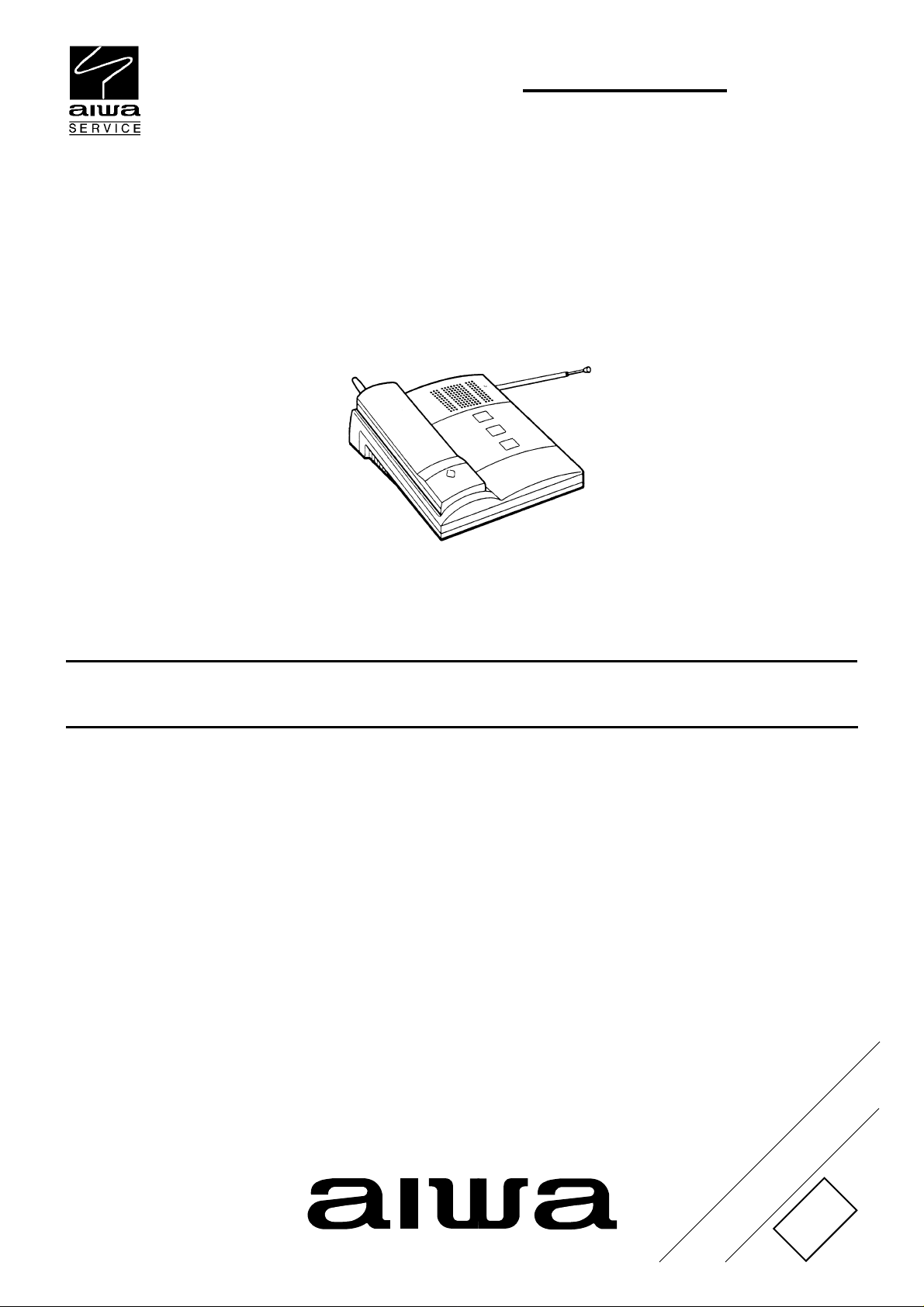
CORDLESS TELEPHONE
This Service Manual is the "Revision Publishing" and replaces "Simple Manual"
(S/M Code No. 09-99B-335-9T1).
This Service Manual does not include "ADJUSTMENT" These items will be
issued in the next Supplement.
S/M Code No. 09-99B-335-9R1
REVISION
DATA
Page 2
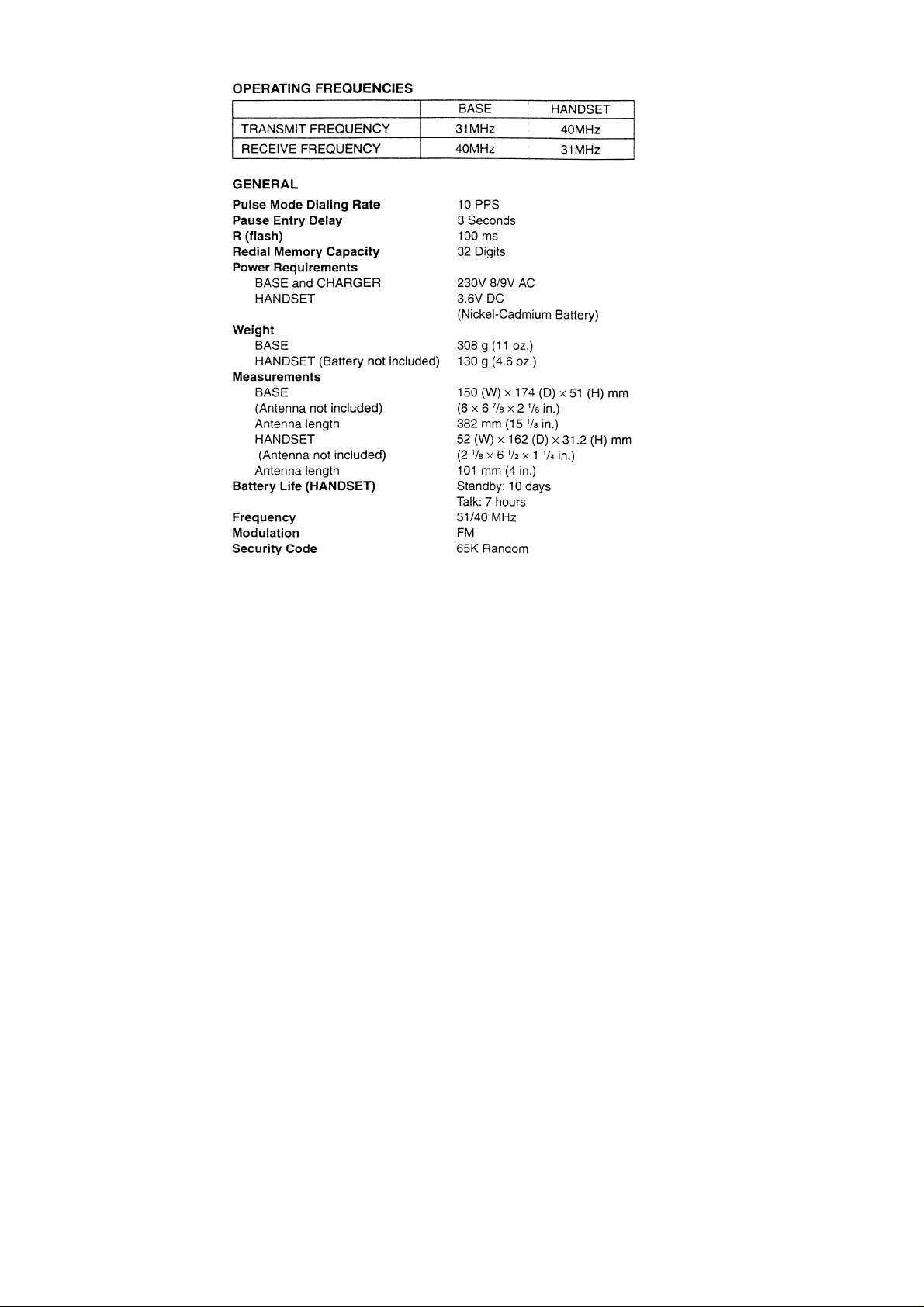
SPECIFICATIONS
Design and specifications are subject to change without
•
notice
.
2
Page 3

ELECTRICAL MAIN PARTS LIST
REF. NO PART NO. KANRI DESCRIPTION
IC
88-PCD-605-010 IC,TB31224F
88-PCD-602-010 IC,TMP87C807U
87-A21-136-040 IC,AT24C01A-10SC 8P
S9-570-290-000 IC,KIA7029F
8Z-PC6-603-010 IC,TMP87C408N
87-A91-033-010 P-COUPLER,LTV817
8Z-PC6-605-010 IC,TEA1062
8Z-PC6-604-010 IC,NJM386D
TRANSISTOR
SA-039-040-000 C-TR,MMBT3904
SA-010-372-000 TR,2SA1037AKQ
SA-038-800-250 TR,KTC3880Y
S3-146-319-525 TR,KTC3195Y
SA-039-060-010 TR,SST3906
8Z-PC6-621-010 TR,KSP92
8Z-PC6-627-080 C-TR,KST42
89-324-121-080 C-TR,2SC2412K
89-327-144-080 TR,2SC2714Y
87-A30-315-080 TR,HIT5609
DIODE
82-135-799-010 DIODE,IN4148
87-A40-587-080 ZENER,BZX55-C5V1 5.1V
S0-100-561-230 ZENER,BZX55-C5V6 5.6V
S0-100-621-210 ZENER,BZX55-C6V2 6.2V
87-A40-583-080 ZENER,BZX55-C5V6
87-A40-246-080 DIODE,IN4148 T-72
87-A40-153-080 ZENER,BZX44/C27
87-A40-586-080 DIODE,1N4004
8Z-PC6-640-080 ZENER,Z1200 200V 1W
87-A40-638-080 ZENER,BZX55-C12
87-A40-145-080 ZENER,BZX55/C7V5
87-A40-585-080 ZENER,BZX55-C6V2
MAIN C.B
BPF301 88-PCD-635-010 FLTR,SFE10.7MS2 -M
BPF302 8Z-PC6-617-010 FLTR,LTW33-450E
BPF303 8Z-PC6-618-010 FLTR,DPX1025 -B/U
C101 87-010-315-080 C-CAP,S 27P-50 CH
C102 87-010-315-080 C-CAP,S 27P-50 CH
C103 87-010-188-080 CAP,CHIP 6800P
C104 87-010-181-080 CAP,CHIP S 1800P
C105 87-010-956-080 CHIP-CAP,S 0.068-25B
C106 87-010-189-080 C-CAP,S 8200P-50 B
C107 87-010-197-080 CAP, CHIP 0.01 DM
C108 87-010-380-040 CAP,E 47-16 SME
C109 87-010-805-080 CAP, S 1-16
C110 87-016-461-080 C-CAP,S 0.47-16F
C111 87-010-178-080 CHIP CAP 1000P
C115 87-010-378-040 CAP,E 10-16
C116 87-010-175-080 CAP 560P
C201 87-A11-064-010 CAP,M/P 0.47-250 K MMCF0250K 4
C202 87-010-198-080 CAP, CHIP 0.022
C203 87-010-976-080 CAP,CER 1000P-500 B
C204 87-010-976-080 CAP,CER 1000P-500 B
C205 87-010-184-080 CHIP CAPACITOR 3300P(K)
C206 87-010-322-080 C-CAP,S 100P-50 CH
C207 87-012-141-080 CHIP-CAPACITOR,0.22-16F
C208 87-010-112-040 CAP,E 100-16
C209 87-010-197-080 CAP, CHIP 0.01 DM
C210 87-010-196-080 CHIP CAPACITOR,0.1-25
C211 87-010-322-080 C-CAP,S 100P-50 CH
C212 87-010-178-080 CHIP CAP 1000P
C213 87-010-196-080 CHIP CAPACITOR,0.1-25
C214 87-010-196-080 CHIP CAPACITOR,0.1-25
NO.
C215 87-010-196-080 CHIP CAPACITOR,0.1-25
C216 87-010-198-080 CAP, CHIP 0.022
C217 87-A10-891-080 CAP,E 4.7-25 SME
C218 87-010-197-080 CAP, CHIP 0.01 DM
C219 87-010-196-080 CHIP CAPACITOR,0.1-25
C220 87-010-197-080 CAP, CHIP 0.01 DM
C221 87-010-198-080 CAP, CHIP 0.022
C224 87-010-378-040 CAP,E 10-16
C301 87-A11-713-080 C-CAP,S 0.039-50 Z F
C302 87-010-178-080 CHIP CAP 1000P
C303 87-012-140-080 CAP 470P
C304 87-010-185-080 C-CAP,S 3900P-50 B
C306 87-010-196-080 CHIP CAPACITOR,0.1-25
C307 87-010-315-080 C-CAP,S 27P-50 CH
C308 87-010-196-080 CHIP CAPACITOR,0.1-25
C309 87-010-189-080 C-CAP,S 8200P-50 B
C310 87-010-196-080 CHIP CAPACITOR,0.1-25
C312 87-010-197-080 CAP, CHIP 0.01 DM
C315 87-010-313-080 CAP, CHIP 18P
C316 87-010-319-080 C-CAP,S 56P-50 CH
C317 87-010-147-080 C-CAP,S 3P-50 CH
C318 87-010-197-080 CAP, CHIP 0.01 DM
C319 87-010-197-080 CAP, CHIP 0.01 DM
C322 87-010-154-080 CAP CHIP 10P
C323 87-A11-112-080 CAP,TC U 1000P-50 J CH
C325 87-010-196-080 CHIP CAPACITOR,0.1-25
C326 87-010-196-080 CHIP CAPACITOR,0.1-25
C327 87-010-315-080 C-CAP,S 27P-50 CH
C328 87-010-197-080 CAP, CHIP 0.01 DM
C329 87-016-461-080 C-CAP,S 0.47-16F
C330 87-010-196-080 CHIP CAPACITOR,0.1-25
C331 87-010-197-080 CAP, CHIP 0.01 DM
C332 87-010-320-080 CHIP CAP 68P
C333 87-010-197-080 CAP, CHIP 0.01 DM
C334 87-010-319-080 C-CAP,S 56P-50 CH
C335 87-010-319-080 C-CAP,S 56P-50 CH
C336 87-010-378-040 CAP,E 10-16
C337 87-010-327-080 CAP, CHIP S 4P SL
C338 87-010-178-080 CHIP CAP 1000P
C339 87-010-196-080 CHIP CAPACITOR,0.1-25
C340 87-010-196-080 CHIP CAPACITOR,0.1-25
C341 87-010-196-080 CHIP CAPACITOR,0.1-25
C342 87-010-314-080 C-CAP,S 22P-50V
C344 87-012-156-080 C-CAP,S 220P-50 CH
C345 87-012-156-080 C-CAP,S 220P-50 CH
C346 87-010-186-080 CAP,CHIP 4700P
C348 87-010-196-080 CHIP CAPACITOR,0.1-25
C349 87-010-185-080 C-CAP,S 3900P-50 B
C350 87-010-196-080 CHIP CAPACITOR,0.1-25
C351 87-010-196-080 CHIP CAPACITOR,0.1-25
C352 87-010-181-080 CAP,CHIP S 1800P
C353 87-A11-747-080 C-CAP,S 0.15-25 Z F
C354 87-010-182-080 C-CAP,S 2200P-50 B
C355 87-A11-747-080 C-CAP,S 0.15-25 Z F
C357 87-010-197-080 CAP, CHIP 0.01 DM
C358 87-010-197-080 CAP, CHIP 0.01 DM
C359 87-010-196-080 CHIP CAPACITOR,0.1-25
C360 87-010-178-080 CHIP CAP 1000P
C361 87-010-318-080 C-CAP,S 47P-50 CH
C364 87-010-178-080 CHIP CAP 1000P
C365 87-012-156-080 C-CAP,S 220P-50 CH
C366 87-010-196-080 CHIP CAPACITOR,0.1-25
C367 87-010-194-080 CAP, CHIP 0.047
C370 87-010-378-040 CAP,E 10-16
C372 87-010-402-040 CAP,E 2.2-50 SME
C373 87-010-992-080 C-CAP,S 0.047-25 B
C374 87-010-378-040 CAP,E 10-16
C376 87-010-402-040 CAP,E 2.2-50 SME
C377 87-010-402-040 CAP,E 2.2-50 SME
C379 87-010-197-080 CAP, CHIP 0.01 DM
REF. NO PART NO. KANRI DESCRIPTION
NO.
3
Page 4

REF. NO PART NO. KANRI DESCRIPTION
C381 87-010-378-040 CAP,E 10-16
C382 87-010-178-080 CHIP CAP 1000P
C383 87-010-112-040 CAP,E 100-16
C384 87-010-380-040 CAP,E 47-16 SME
C386 87-010-597-080 C-CAP,S 0.056-16V,RK
C390 87-010-312-080 C-CAP,S 15P-50 CH
C391 87-010-312-080 C-CAP,S 15P-50 CH
C501 87-010-976-080 CAP,CER 1000P-500 B
C502 87-010-976-080 CAP,CER 1000P-500 B
C503 87-010-976-080 CAP,CER 1000P-500 B
C504 87-010-976-080 CAP,CER 1000P-500 B
C505 87-010-388-010 CAP, ELECT 1000-25SME
C506 87-010-178-080 CHIP CAP 1000P
C507 87-010-235-040 CAP,E 470-16 M 11L SME
C508 87-010-380-040 CAP,E 47-16 SME
C509 87-010-178-080 CHIP CAP 1000P
C510 87-010-976-080 CAP,CER 1000P-500 B
C512 87-010-976-080 CAP,CER 1000P-500 B
C514 87-010-101-010 CAP,E 220-16 SME
C515 87-010-197-080 CAP, CHIP 0.01 DM
J201 88-PCD-615-010 JACK,MODULAR 2 P E5562-000111
J501 8Z-PC6-611-010 JACK,MODULAR 6 P E5764-0003P3
L101 8Z-PC6-620-080 COIL,100UH K LAL02
L102 8Z-PC6-620-080 COIL,100UH K LAL02
L201 87-005-126-080 COIL,1MH
L202 87-005-126-080 COIL,1MH
L301 87-A50-472-010 COIL,0.72UH K KYN
L302 87-A50-368-010 COIL,0.33UH K KYN
L304 8Z-PC6-626-080 COIL,3.9UH K LAL02
L305 87-A50-474-010 COIL,2.7UH LAL03
L306 87-A50-473-010 COIL,0.82UH K KYN
L307 87-A50-447-010 COIL,37UH K 5M4A756N
L308 88-PCD-656-010 COIL,182 46MHZ
L309 87-005-272-080 COIL,22UH
L310 87-005-230-080 COIL,0.56UH M LAL03
L501 87-005-239-080 COIL,100UH
L502 87-005-239-080 COIL,100UH
L503 87-005-239-080 COIL,100UH
L504 87-005-239-080 COIL,100UH
L505 87-005-239-080 COIL,100UH
L506 87-005-239-080 COIL,100UH
LED101 88-PCD-655-080 LED,SE-3001DT RED
LED102 88-PCD-655-080 LED,SE-3001DT RED
SCR201 87-A91-039-010 VRIS,SAS-391KD07
SCR301 87-A40-226-080 VARI-CAP,SVC251SPA
SFR303 87-A91-035-080 SFR,100K H EVNDXAA03B15
SW101 87-A91-036-010 SW,SL 2-2-2 SKA-22D10-G4-NA
SW102 8Z-PC6-623-010 SW,TACT 1102-4
TC301 87-A91-180-010 TRIMMER,30P CVN6D030A
X101 8Z-PC6-622-010 VIB,6.00MHZ ZTA6.00MT
NO.
X301 8Z-PC6-615-010 VIB,11.15MHZ HC-49/U
HS-RF C.B
C12 87-010-075-040 CAP,E 10-16V
C15 87-010-380-010 CAP,E 47-16V
C16 87-015-696-080 CAP,E 2.2-50V
C19 87-010-545-010 CAP,E 0.22-50V
C24 87-010-075-040 CAP,E 10-16V
C30 87-015-696-080 CAP,E 2.2-50V
C33 87-010-380-010 CAP,E 47-16V
C65 87-010-400-010 CAP,E 0.47-50V
C85 87-010-380-010 CAP,E 47-16V
C87 87-010-264-040 CAP,E 100-10V
D1 87-A40-226-080 DIODE,SVC251SPA
DX1 S3-001-650-000 DUPLEXER 31/40MHZ
IFT1 S0-002-860-070 IFT,KL286N
IFT2 S0-075-600-070 IFT,7MM 455KHZ
IFT3 S0-002-760-070 IFT,KL276N
IFT4 S0-002-741-070 IFT,KL274N
IFT5 S0-002-770-070 IFT,KL277N
J1 S0-200-2P1-500 HEADER KINDTECH 15P
L1 87-003-106-010 INDUCTOR,0.33UH
L2 87-005-166-010 INDUCTOR,1.2UH
L3 87-005-674-080 INDUCTOR,1.5UH
L4 S0-100-152-010 INDUCTOR,10UH
L5 87-003-133-010 INDUCTOR,0.22UH
T1 S0-004-500-180 CER,FILTER LTW33-450E
VR1 S1-030-850-000 SFR,10K
VR3 S1-030-850-000 SFR,10K
X1 S6-111-501-000 X’TAL,11.15MHZ
X2 S0-001-070-010 CER,FILTER 10.7MHz
X3 S3-327-681-000 X’TAL,32.768KHZ
X4 S0-006-000-010 CER,FILTER 6.00MHz
HAND KEY C.B
B1 SB-2BE-HA0-200 HEADER JST 2PIN
L1 87-003-150-080 INDUCTOR 68UH
L2 87-003-150-080 INDUCTOR 68UH
LED1 S0-321-610-010 C-LED,3.2-1.6(RED)
LED2 S0-321-610-010 C-LED,3.2-1.6(RED)
LED3 S0-049-410-030 LED,3MM(GRN)
LED4 S0-049-410-030 LED,3MM(GRN)
LED5 S0-049-410-030 LED,3MM(GRN)
LED6 S0-049-410-030 LED,3MM(GRN)
REF. NO PART NO. KANRI DESCRIPTION
NO.
• Regarding connectors, they are not stocked as they are not the initial order items.
The connectors are available after they are supplied from connector manufacturers upon the order is received.
4
Page 5
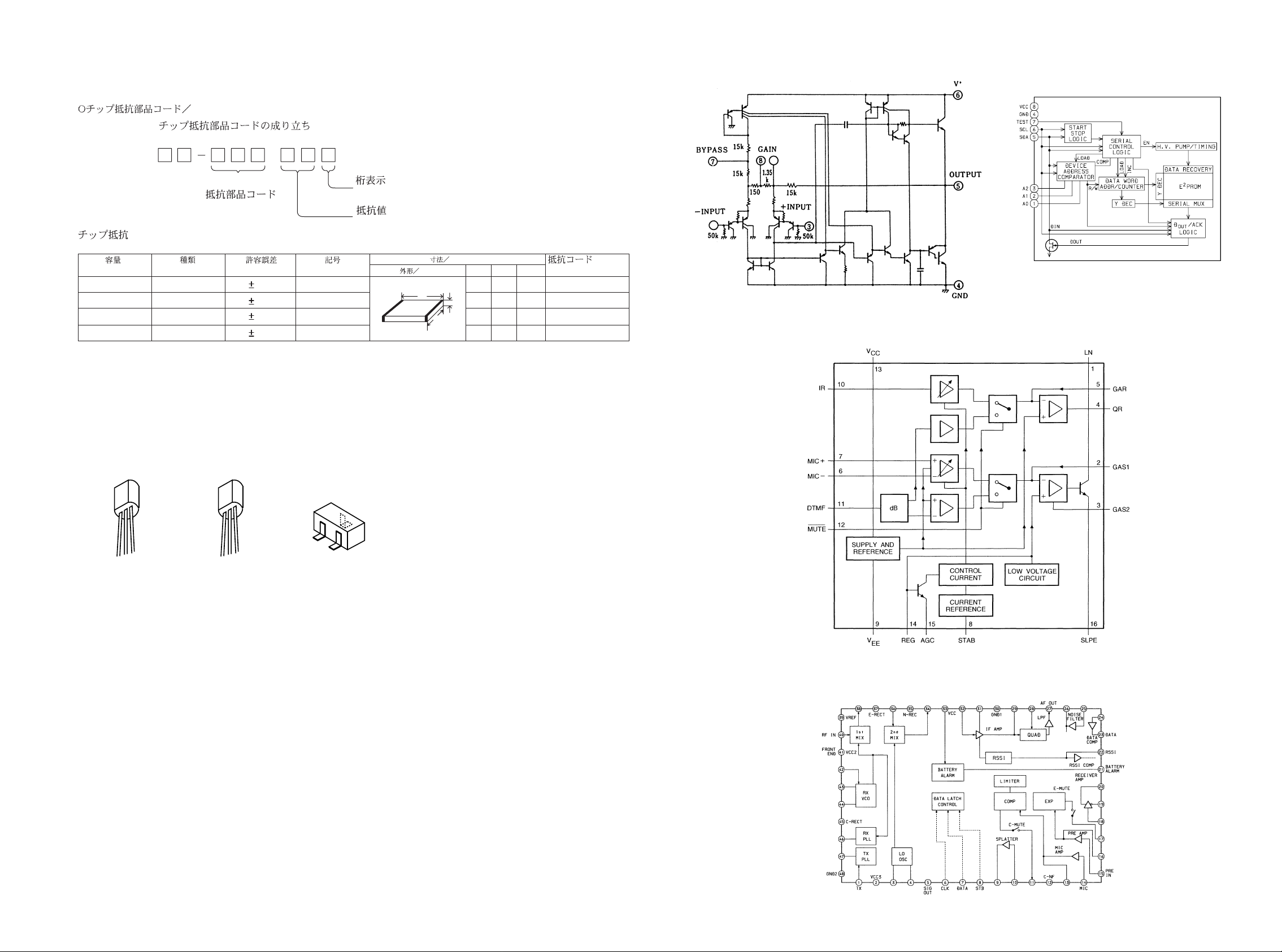
CHIP RESISTOR PART CODE
Chip Resistor Part Coding
88
IC BLOCK DIAGRAM
IC, NJM386D
IC, AT24C01A-10SC
A
Resistor Code
Chip resistor
Wattage Type Tolerance
1/16W 1005 5% CJ
1/16W
1/10W
1/8W
1608
2125
3216
5%
5%
5%
TRANSISTOR ILLUSTRATION
Symbol
CJ
CJ
CJ
Figure
Value of resistor
Form
L
C
Dimensions (mm)
t
W
0.55
Resistor Code
108
118
128
LW t
1.0 0.5 0.35 104
1.6 0.8 0.45
2 1.25 0.45
3.2
1.6
: A
: A
IC, TEA1062
E C B E B C
2SC2714
KSP92 2SA1037
KTC3195
HIT5609
B
E
KTC3880
MMBT3904
SST3906
2SC2412
KST42
IC, TB31224F
65
Page 6
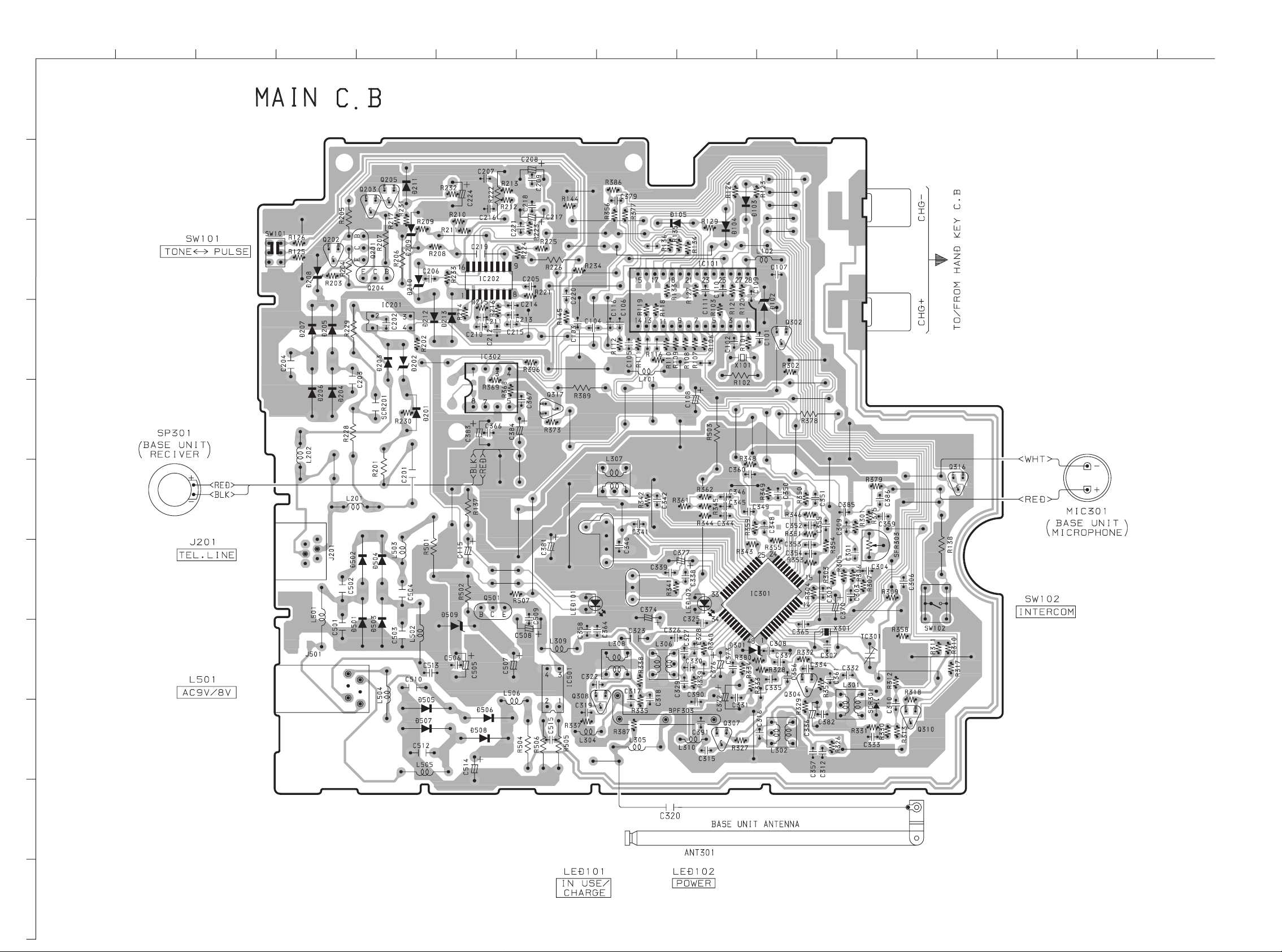
WIRING-1 (MAIN)
1
A
B
C
D
234567
8
9
10
11 12 13
14
E
F
BPF302
G
BPF301
H
I
J
K
87
Page 7
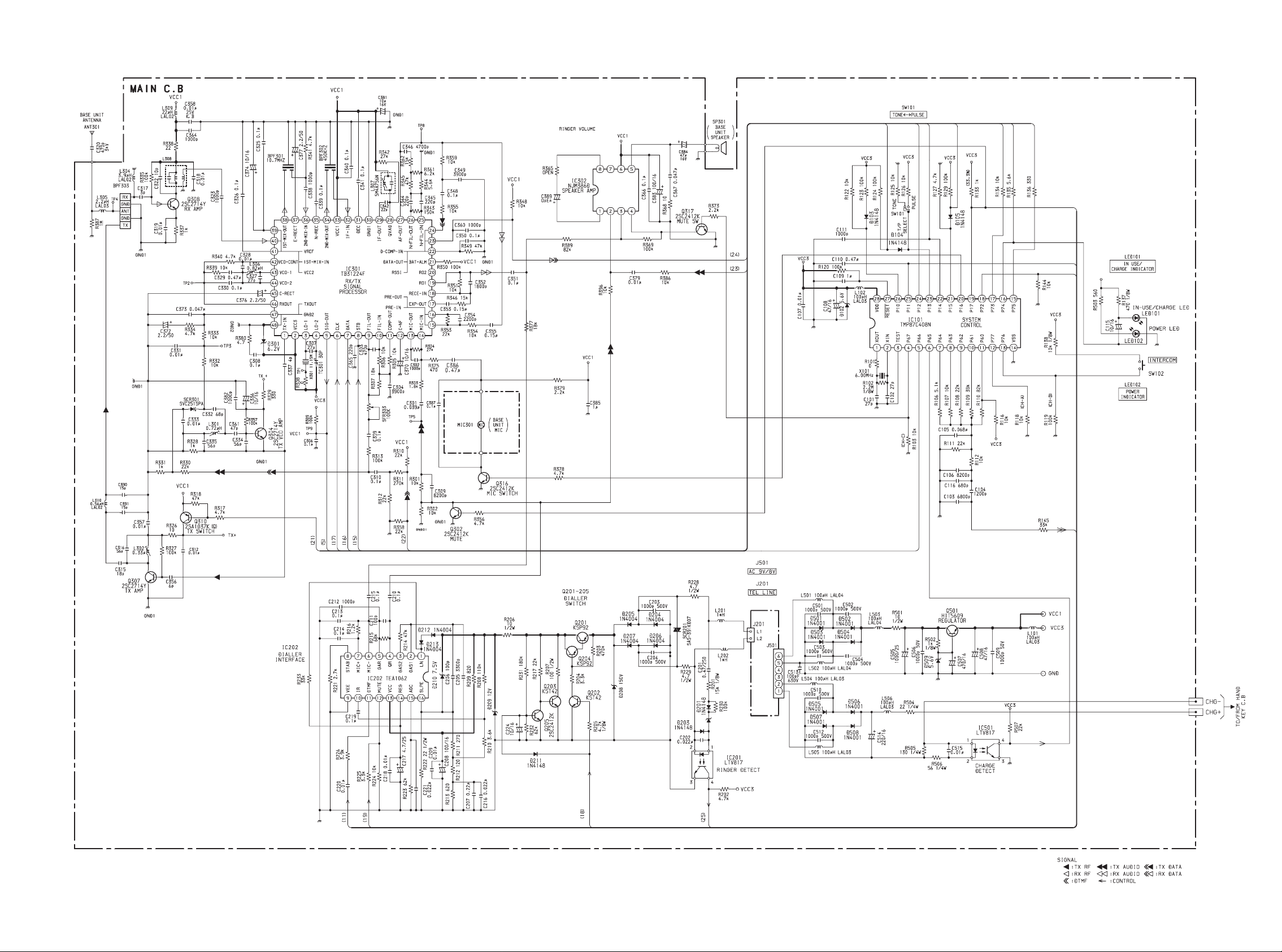
SCHEMATIC DIAGRAM-1 (MAIN)
DPX1025
GAIN
GAIN
BY
PASS
–INPUT
V+
+INPUT
OUTPUT
GND
D202
BZX44/C27
109
Page 8
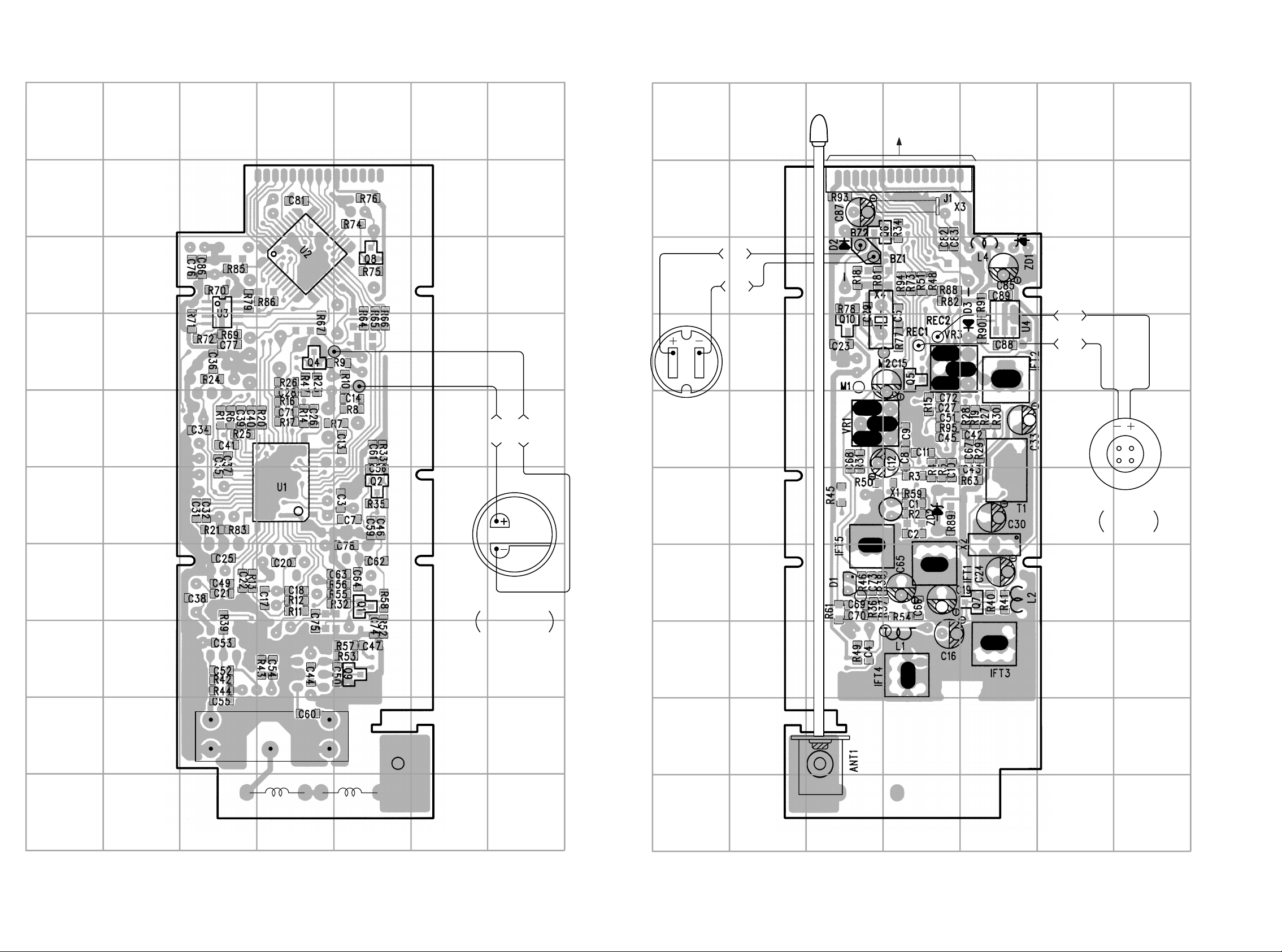
WIRING-2 (HS-RF: COMPONENT)
WIRING-3 (HS-RF: CONDUCTOR)
7
6
5
HS-RF C.B
1
8
45
432
(COMPONENT SIDE)
33
34
44
1
11 12
23
22
1
A
B
C
D
A
B
C
D
1
RED
BLK
2
HS-RF C.B
HANDSET
ANTENNA
3
456
(CONDUCTOR SIDE)
TO/FROM
HAND KEY C.B
115
RED
13
BLK
7
25
38
39 48
DX1
BZ1
(HANDSET RINGER)
BLK
1524
14
1
RED
M1
HANDSET
MICROPHONE
E
F
G
H
I
E
F
G
H
I
SP1
HANDSET
RECIVER
L5 L3
J
J
1211
Page 9

SCHEMATIC DIAGRAM-2 (HS-RF 1/3)
SQ
SELECTION
TX DATA
CHARGE DET
RX DATA
LB LED VDD
TALK LED XTOUT
PC13 ZPC7 XTIN
KEY LED FN COL
BATT ALARM VOL HI
N.C. VOL LO
CLK
EEPROM
RX PWR BUZZER
TEST ROW3
RESET ROW2
COL0
COL1
COL2
COL3
SIG OUT
OUT
1
5
10
15
XIN ROW1
XOUT ROW0
GND N.C.
N.C. N.C.
PLL STB RING VOL
PLL DATA
DI EEPROM
DO EEPROM
PLL CK
BAND
TX PWR
COUNTRY
COUNTRY
S2
S1
OSC
SWITCH
1413
Page 10

SCHEMATIC DIAGRAM-3 (HS-RF 2/3)
7MM
455kHz
1615
Page 11

SCHEMATIC DIAGRAM-4 (HS-RF 3/3)
1817
Page 12

WIRING-4 (HAND KEY)
3MM
3MM
3MM
3MM
LED
DRIVER
3.2-1.6
3.2-1.6
Ni-cd
BATTERY
3.6V
TO/FROM MAIN C.B
1
A
234567
HAND-KEY C.B
SCHEMATIC DIAGRAM-5 (HAND KEY)
TO/FROM HS-RF C.B
CON1
CON1
B
R5R4R3
R13
SW15
LED2
R14
C
D
R8
R7
R12
R1
R2
R15
SW18SW17
R9
115
R6
E
D5
LED1
SW19
C
SW1
Q1
R10
R11
B
LED2
TALK
SW15
TALK
SW17
1
LED1
BATT. LOW
SW1
MEMORY
SW18
2
SW19
3
E
LED4 LED3
SW14SW13SW12
SW12
4
SW13
5
SW14
6
F
SW7 SW8 SW9
SW7
7
G
LED5 LED6
SW4SW3SW2
1
1
BLK
2
2
B1
SW10
SW11
SW6 SW16
C5
D3
D2
C1
L2
SW5
D4
C4
ZD2
CHG1CHG2
D1
ZD1
SW20
C2
L1
H
RED
I
Nickel-Cadmium Battery
J
3.6V DC
(KEY BACK LIGHT)
SW2
SW11
R/P
SW10
VOL
SW8
8
LED3,4,5,6
SW3
0
SW6
R
SW5
STORE
SW9
9
SW4
#
SW16
CH
SW20
INTERCOM
TO/FROM MAIN C.B
K
2019
Page 13

IC DESCRIPTION
IC, TMP87C408N
Pin No. Pin Name I/O Description
1
2
3
4
5
6
7
8-10
XOUT
XIN
TEST
HOOK CONT
SPK MUTE
SIG OUT
CHAG DET
CLK EEPROM
DTMF4
DTMF3-DTMF1
I/O
Oscillator out
O
Oscillator in
I
Tied low
I
Hook control output (for corded phone): 0 = OFF HOOK, 1 = ON HOOK
For ZPC-6: this pin is used as Speaker Amp, IC Mute Control)
O
(the Mic Mute control is controlled by hardware: unmute mic when Speaker is unmute
and charge not detected)
Received Signal Strength Indicator: (TB31224F SIG OUT pin)
0 = carrier present, 1 = carrier absent NOISE DETECT
I
0 = Rx unlock, 1 = Rx lock Rx LOCK DETECT
0 = Tx unlock, 1 = Tx lock Tx LOCK DETECT
Charge detect: 0 = charging, 1 = not charging.
Clock of EEPROM
DTMF data pin 4 (Most Significant Bit)
O
DTMF data pin 3-1
O
11
12
13
14
15
16
17
18
19
20
21
22
DTMF0
COUNTRY S2
RING OFF
COUNTRY S1
PAGE KEY
GND
PLL STB
PLL DATA
U LED
PLL CK
DO EEPROM DI EEPROM
TL RELAY
TL MUTE
M B SEL
HOOK DET
TX PWR
SCRET OPT
TX DATA
I/O
I/O
—
I/O
I/O
I/O
DTMF data pin 0 (Least Significant Bit)
Country option select 2.
Control the shunt resistor: 1 = shunt a resistor (For U, K ONLY)
Country option select 1
PAGE key: 1 = PAGE ON, 0 = STANDBY
I
Ground
Combo chip strobe signal (TB31224F)
O
Combo chip data signal (TB31224F).
O
In-use LED: 1 = ON, 0 = OFF.
Combo chip clk signal (TB31224F).
Data Input/Output of EEPROM.
Line seize: 1 = line seize, 0 = off-hook
O
Telephone Line Mute Control: 1 = MUTE.
Make/Break Ratio Select 1 = 33.3%, 0 = 40%
Hook detect input (for Corded Phone). 1 = ON HOOK, 0 = OFF HOOK
REMARK: this pin is always PULL-HIGH for ZPC-7 or ZPC-6 (I. e. just imagine
I
Corded phone is Always ON HOOK)
Tx power control: 0 = ON, 1 = OFF. Secret function option: 1 = YES, 0 = NO
REMARK: this PULL LOW for ZPC-7 or ZPC-6 (I. e. Secret opt is DISABLED)
Transmit data output
O
23
24
25
26
27
28
BUZZER
T P SEL
RX DATA
RING DET
BAND
SQ SELECTION
____________
RESET
POWER
I/O
I/O
—
Buzzer signal (key tone and paging sound ONLY)
Tone/Pulse selection: 1 = Pulse, 0 = Tone
Received data input
I
Ring detect input: 1 = OFF, 0 = RING COME (MC34012)
I
Shunt capacitor for U.S. Frequency Higher Band: 1 = shunt Cap, OUT OF RANGE
FUNCTION: 1 = YES, 0 = NO
Normally High, Low to reset MCU
I
Power (VCC)
21
Page 14

IC, TB31224F
Pin No. Pin Name I/O Description
1
2
3, 4
TX-IN
VCC3
LO-1, LO-2
I
Input terminal of TX VCO oscillation signal.
—
Power supply terminal.
LOCAL OSCILLATOR input and output terminals. Colpitts oscillator is formed by
O
internal emitter follower and external X’tal. And external injection is possible from pin
3.
10
11
12
13
14
15
16
17
18
19
20
5
6
7
8
9
SIG OUT
CLK
DATA
STB
FIL-OUT
FIL-IN
COMP-OUT
C-NF
MIC-OUT
MIC-IN
PRE-IN
PRE-OUT
EXP-OUT
RECE-IN
RO1
RO2
O
Output terminal of detection signal. It is the open drain output.
I
Input terminal of clock.
I
Input terminal of serial data. Input the serial data for controlling IC.
I
Input terminal of strobe signal.
O
Output of FILTER AMP.
I
Input of FILTER AMP.
O
Output of COMPRESSOR.
—
Feedback circuit of T type is formed by external capacitor with SUM AMP.
O
Output of MIC AMP and connected directly to input of SUM AMP.
I
Input terminal of MIC AMP.
I
Inverted input of PRE AMP.
O
Output of PRE AMP. Connected directly to EXPANDER.
Output of SUM AMP at EXPANDER. The signal from gain cell is gained by inverted
O
amp.
I
Inverted input of RECEIVER AMP.
O
Receiving output for a dynamic receiver.
O
Used for BTL output type with RO1 terminal when a ceramic receiver is used.
21
22
23
24
25
26
27
28
29
30
31
32
33
BAT-ALM
RSS1
DATA-OUT
D-COMP-IN
N FIL-IN
N FIL-OUT
AF-OUT
QUAD
IF-OUT
GND1
DEC
IF-IN
VCC1
BATTERY ALARM terminals. When VCC decrease VBAT-L, This terminal outputs
O
“H” level. Detection voltage is controlled by data bit. This terminal is open collector
output.
This terminal outputs DC level according to input signal level to IF AMP. Dynamic
O
range is around 70dB.
O
Output terminal for wave form shaping. This terminal is open collector output.
DATA COMPARATOR input terminal. This terminal input demodulation signal of
I
DATA.
I
NOISE FILTER input and output terminals. BPF is composed of external capacitors
O
and resistors. Connected internally to rectifier circuit by coupling capacitor.
Demodulated signal output terminal. Carrier leak is small as LPF is built-in. Output
O
impedance is around 360Ω.
I
Phase shift signal input terminal of FM demodulator.
O
Output terminal of IF AMP.
—
GND terminal.
I
2nd IF input and decoupling for bias. Input impedance is around 1.5kΩ.
I
—
Power supply terminal.
34
2ND MIX-OUT
O
MIX output terminal. Output impedance is around 1.5kΩ.
22
Page 15

Pin No. Pin Name I/O Description
35
36
37
N-REC
2ND MIX-IN
E-RECT
After output of NOISE FILTER amplified around 20dB, noise signal is rectified by
O
external capacitor.
I
1st IF signal input terminal. Input impedance is around 4.7kΩ at 10.695MHz.
O
Connected capacitor for full-wave rectifier circuit of EXPANDER.
38
39
40
41
42
43, 44
45
46
47
48
1. General description
TB31224F is controlled by serial parts pin 6, 7, 8, and makes all situations by these serial bits for RF part in 46/49MHz cordless
telephone such as intermittent receiving state.
Not only 46/49MHz cordless telephone but CT0 cordless phone that has frequency spec. between about 20MHz and 60MHz can
be also set up TB31224F.
1ST MIX-OUT
VREF
1ST MIX-IN
VCC2
VCO-CONT
VCO-1, VCO-2
C-RECT
RX-OUT
TX-OUT
GND2
—
—
—
—
O
MIX output terminals. Externally connects filters. Output impedance is 330Ω. (Typ.)
Reference terminal through internal buffer of compander block.
I
MIX input terminal. Double-balance MIX.
Regulator terminal. Output voltage is 2.0V.
I
Voltage control terminal of RX-VCO.
I
They are resonance terminals of RX-VCO.
Terminal for rectifier of COMPRESSOR. Almost the same circuit as E-RECT
terminal.
O
Output terminal of CHARGE PUMP. CHARGE PUMP is constant current output
O
circuit, and output current is varied by input serial data.
GND terminal.
23
Page 16

IC, TMP87C807U
Pin No. Pin Name I/O Description
I
OUT OF RANGE FUNCTION: 1 = YES, 0 = NO
O
Transmitted data
I
Charge detect: 1 = charging, 0 = not charging
I
Received data (INT3/TC3)
O
Low battery led (High current port): 1 = ON
O
Talk led (High current port): 0 = ON
I
Power save mode. Hi: NO, Lo = YES
O
Keypad LED: 0 = ON
Battery low detect: 0 = battery ok, 1 = battery low (3.25 V).
I
(Use COMBO chip TB31224F battery detect function)
—
Not connected.
O
Clock of EEPROM
O
Rx power control : 0 = ON, 1 = OFF.
—
Tied to low
I
Normally High, low to reset MCU.
I
Resonator in (3.58 MHz)
O
Resonator out (3.58 MHz)
—
Ground
—
Not connected.
10
11
12
13
14
15
16
17
18
1
2
3
4
5
6
7
8
9
SQ SELECTION
TX DATA
CHARGE DET
RX DATA
LB LED
TALK LED
PC13 ZPC7
KEY LED
BATT ALARM
N.C.
CLK EEPROM
RX PWR
TEST
______
RESET
XIN
XOUT
GND
N.C.
19
20
21
22
23, 24
25
26
27, 28
29-32
33
34
35
36
37
PLL STB
PLL DATA
DI EEPROM
DO EEPROM
PLL CK
BAND
COUNTRY S1, S2
TX PWR
RING VOL
N.C.
ROW0-ROW3
BUZZER OUT
SIG OUT
VOL LO
VOL HI
FN COL
O
I/O
O
O
I
O
O
—
O
O
I
O
O
I
Combo chip strobe signal input.
Combo chip data signal input.
Data input of EEPROM.
Data output of EEPROM.
Combo chip clock signal output.
Shunt capacitor for U.S. frequency high band: 1 = shunt capacitor.
Country channel table selection 1, 2.
TX power control : 0 = ON, 1 = OFF.
Ringer volume control
Not connected.
Keypad column output #0-#3
Buzzer signal
Received signal strength indicator: (TB31224F SIG OUT Pin)
0 = carrier present, 1 = carrier absent
0 = Rx unlock, 1 = Rx lock
0 = Tx unlock, 1 = Tx lock
Receiver volume control 1 (Lo)
Receiver volume control 2 (Hi)
Function key column input (INT5)
38
39
40
41-44
XTIN
XTOUT
VDD
COL3-COL0
I
32.768 kHz crystal
O
32.768 kHz crystal
—
Power (VCC)
I
Keypad column input #0-#3
24
Page 17

VOLTAGE CHART
< B/U-MAIN >
IC302 (SPEAKER-AMP)
WAITING (V) TALIKING (V) CHARGING (V)
1 3.5 3.5 3.5
2 3.1 3.1 3.1
3 3.7 3.7 3.7
4 3.7 4 3.7
5 4.2 4.2 4.2
6555
7 3.7 3.7 3.7
8 3.5 3.5 3.5
IC202 (SPEACH)
WAITING (V) TALIKING (V) CHARGING (V)
1 0 3.7 0
2 0-0.1 2 0-0.1
3 0-0.1 2 0-0.1
4 0.3 2.2 0.2
5 0.2 2.2 0.2
6 0.2 2.2 0.2
7 0.2 2.2 0.2
8 0 0.1 0
9000
10 0.2 1.2 0.2
11 0.1 2.2 0.1
12 0.2 0.2 0.2
13 0 4.4 0
14020
15 0 0.8 0
16 0 0.8 0
IC301 (RF)
WAITING (V) TALIKING (V) CHARGING (V)
1555
2555
3 4.9 4.9 4.9
4 4.6 4.6 4.6
5 4.9 0.02 4.9
6 0.02 0 0.03
7 4.8 0.4 0.4
8000
9 0.7 1.4 0.7
10 0.7 1.4 0.7
11 0.7 1.4 0.7
12 0.8 1.4 0.8
13 0.8 1.4 0.8
14 0.8 1.4 0.8
15 1.5 1.4 1.4
16 1.5 1.4 1.4
17 1.5 1.4 1.4
18 1.2 1.2 1.2
19 1.2 1.2 1.2
20 1.2 1.2 1.2
21 0.01 0 0.01
22 0.4 1.1 0.4
23 2.4 2.5 2.5
24 0.7 0.7 0.7
25 0.6 0.6 0.6
26 0.7 1.5 0.7
27 1-1.2 1.1 1
28555
29 4.1 4.1 4.1
30000
31 4.6 4.6 4.6
32 4.6 4.6 4.6
33555
34 3.6 3.7 3.6
35 1.2 0.06 1.2
36111
25
Page 18

IC201 (MCU)
WAITING (V) TALIKING (V) CHARGING (V)
37 1.3 0.7 1.3
38 3.5 3.7 3.5
39 1.5 1.5 1.5
40111
41 2.1 2.1 2.1
42 2.1 2.1 2
43555
44555
45 0.3 0.7 0.3
46 2 2.1 2.1
47 1.3 3.7 2
48000
WAITING (V) TALIKING (V) CHARGING (V)
1 2.1 2.1 2.1
2222
3000
4000
5 4.9 0.02 4.9
6 4.9 4.9 0.03
7000
8000
9000
10000
11 0.03 0.03 0.03
12000
13000
14000
15000
16 4.8 0.4 0.4
17 0.03 0 0.03
18 0 4.6 0
19 0.3 0.3 0.3
20 0.01 0.01 0.01
21 4.7 0.06 4.7
22 2.4 2.4 2.4
23555
24 2.5 2.5 2.4
25555
26 0-0.04 0.05 0-0.4
27 4.8 4.8 4.8
28 4.8 4.8 4.8
26
Page 19

Q201
Q304
WAITING (V) TALIKING (V) CHARGING (V)
E 49.4 6.4 49.2
C 0 5.6 0
B 47.3 56 47.1
Q202
WAITING (V) TALIKING (V) CHARGING (V)
E000
C 29.8 0.01 30.1
B 0 0.7 0
Q203
WAITING (V) TALIKING (V) CHARGING (V)
E000
C 0 5.6 0
B 0 0.5 0
Q204
WAITING (V) TALIKING (V) CHARGING (V)
E 0 2.1 0
C 0.2 4.3 0.2
B 0.2 2.6 0.2
Q310
WAITING (V) TALIKING (V) CHARGING (V)
E555
C 0.3 4.9 0.3
B 4.9 4.3 4.9
Q307
WAITING (V) TALIKING (V) CHARGING (V)
E000
C 0.2 4.9 0.2
B 0.2 0.6 0.2
Q308
WAITING (V) TALIKING (V) CHARGING (V)
E 47.4 5.6 47.2
C 0 5.6 0
B 30.1 4.9 29.1
Q205
WAITING (V) TALIKING (V) CHARGING (V)
E000
C 0 0.5 0
B 0 0.6 0
Q316
WAITING (V) TALIKING (V) CHARGING (V)
E000
C 0.1 0.1 0.2
B 0.01 0.01 0.01
Q302
WAITING (V) TALIKING (V) CHARGING (V)
E 2.3 2.3 2.3
C 4.9 4.9 4.9
B 2.7 2.6 2.7
Q317
WAITING (V) TALIKING (V) CHARGING (V)
E000
C 3.7 4 3.7
B000
Q501
WAITING (V) TALIKING (V) CHARGING (V)
E555
C 10.8 10.3 10.2
B 5.6 5.6 5.6
WAITING (V) TALIKING (V) CHARGING (V)
E000
C 1.5 1.5 1.5
B 0.3 0.3 0.3
27
Page 20

< H/S-RF >
IC-U4 (RESET)
WAITING (V) TALIKING (V) CHARGING (V)
1 3.8 3.8 3.8
2000
3 3.8 3.8 3.8
IC-U2 (MCU)
WAITING (V) TALIKING (V) CHARGING (V)
1000
2000
3 0 0 4.4
4 3.8 0-2.8 1.8
5 3.8 3.8 4.1
6 0 3.5 0
7 3.8 3.8 4.1
8 3.8 3.8 4.1
9 3.8 0.02 0.02
10 1.8 1.5 0
11000
12 3.8 0.02 0.02
13000
14 3.8 3.8 4.1
15 0-3 1.2 1.4
16 3.8 1.5 1.6
17000
18 1.5 1.4 0-0.01
19000
20 3.8 3.8 4.1
21000
22 0 0 0-2.1
23 0 0 0.04
24 3.8 3.8 4.1
IC-U3 (EEPROM)
WAITING (V) TALIKING (V) CHARGING (V)
1 3.8 3.8 3.8
2000
3 3.8 3.8 3.8
4000
5 3.8 3.8 3.8
6000
7000
8 3.8 3.8 3.8
WAITING (V) TALIKING (V) CHARGING (V)
25 3.8 0.04 4.1
26 3.8 3.8 4.1
27 1.5 1.5 0-0.01
28 1.5 1.5 0-0.01
29000
30000
31000
32000
33000
34 3.8 3.8 4.1
35 0 3.8 0
36 3.8 0 4.1
37 3.8 3.8 4.1
38 1.3 1.3 1.5
39 2 2 2.2
40 3.8 3.8 4.1
41 3.8 3.8 4.1
42 3.8 3.8 4.1
43 3.8 3.8 4.1
44 3.8 3.8 4.1
28
Page 21

IC-U1 (RF)
WAITING (V) TALIKING (V) CHARGING (V)
1 3.8 3.7 3.9
2 3.8 3.7 3.9
3 0-1.4 3.7 3.9
4 0-1.4 3.3 3.5
5 3.8 0.03 4
6 0 0 0.04
7 3.8 3.8 4
8000
9 0.1 1.4 0.1
10 0.1 1.4 0.1
11 0.3 1.4 0.3
12 0.3 1.4 0.3
13 0.3 1.4 0.3
14 0.3 1.4 0.3
15 0-0.2 1.4 0.01-0.2
16 0-0.2 1.4 0.01-0.2
17 0.1 1.4 0.1
18 0.01-0.1 1.2 0.1
19 0.01-0.1 1.2 0.1
20 0.01-0.1 1.2 0.1
21 0-3.8 0 0.02
22 0 1 0.2
23 0-3.8 0.01-1.8 1.8
24 0-0.06 0.7 0.7
25 0 0.7 0.7
26 0 0.7 0.7
27 0.01-0.8 0.7 1
28 0.1-1.1 3.8 4
29 0.1-1 2.8 3.1
30000
31 0.1-1.2 3.4 3.6
32 0.1-1.2 3.4 3.6
WAITING (V) TALIKING (V) CHARGING (V)
33 0.1-1.2 3.8 4
34 0.1-0.9 2.4 2.7
35 0 0.05 1.3
36 0.01-0.4 1 1
37 0.3 0.7 0.3
38 0.1-0.8 2.3 2.6
39 0.3 1.4 0.3
40 0-0.1 1 1
41 0.3-1.8 2 2
42 0-0.6 0.02 0-0.6
43 0.1-1.1 3.8 4
44 0-0.1 3.8 4
45 0.3 0.6 0.3
46 0-0.8 1.1 2.3
47 0.07 2.2 0.2
48000
29
Page 22

Q3
Q2
WAITING (V) TALIKING (V) CHARGING (V)
E 0-0.2 0.8 0.8
C 0.1-1.2 3.5 3.5
B 0.5-1.5 1.5 1.5
Q7
WAITING (V) TALIKING (V) CHARGING (V)
E 3.8 3.8 3.9
C 0.1-1.8 3.7 3.8
B 3.8 3.1 3.2
Q5
WAITING (V) TALIKING (V) CHARGING (V)
E000
C 0.02 0.02 0.02
B 0 0.5 0
Q6
WAITING (V) TALIKING (V) CHARGING (V)
E 0 1.3 0
C 0.2 2.6 0.1
B 0.2 2 0.1
Q1
WAITING (V) TALIKING (V) CHARGING (V)
E 0 0.2 0
C 0.2 3.4 0.1
B 0.2 1 0.1
Q9
WAITING (V) TALIKING (V) CHARGING (V)
E000
C 0.2 3.5 0.1
B 0.2 0.7 0.1
Q1
WAITING (V) TALIKING (V) CHARGING (V)
E000
C 3.8 3.8 3.9
B000
Q10
WAITING (V) TALIKING (V) CHARGING (V)
E 3.8 3.8 3.9
C 0.2 3.7 0.1
B 3.8 3.1 3.9
Q8
WAITING (V) TALIKING (V) CHARGING (V)
E 3.8 3.8 3.9
C 3.8 3.8 3.9
B 3.8 3.8 3.9
Q4
WAITING (V) TALIKING (V) CHARGING (V)
E 3.8 1.5 4
C000
B 3.8 3.8 4.1
WAITING (V) TALIKING (V) CHARGING (V)
E000
C 0.04 0.04 0.04
B 0.6 0 0.6
30
Page 23

MECHANICAL EXPLODED VIEW 1/2
MECHANICAL PARTS LIST 1/2
12
1
2
a
7
13
D
a
5
4
A
3
11
10
12
6
B
B
C
B
REF. NO PART NO. KANRI DESCRIPTION
NO.
1 88-PCD-006-010 HANGER,H/S BLK B/U<AEZ1B>
1 88-PCD-124-010 HANGER,H/S BLUE B/U<AEZ1L>
1 88-PCD-154-010 HANGER,H/S GRN B/U<AEZ1G>
2 8Z-PC6-001-010 CABI,TOP BLK B/U<AEZ1B>
2 8Z-PC6-031-010 CABI,TOP BLUE B/U<AEZ1L>
2 8Z-PC6-041-010 CABI,TOP GRN B/U<AEZ1G>
3 88-PCD-205-010 TERMINAL,ANT B/U
4 8Z-PC6-004-010 LENS,LED BLK
5 8Z-PC6-003-010 BTN,INT BLK B/U
6 8Z-PC6-201-010 HLDR,BTN B/U
7 8Z-PC6-203-010 TERMINAL,CHG B/U
8 8Z-PC6-002-010 CABI,BOTTOM BLK B/U
8 8Z-PC6-032-010 CABI,BOTTOM BLUE B/U<AEZ1L>
8 8Z-PC6-042-010 CABI,BOTTOM GRN B/U<AEZ1G>
9 88-PCD-202-010 FOOT,RUBBER
COLOR NAME TABLE
Basic color symbol Color Basic color symbol Color Basic color symbol Color
B Black C Cream D Orange
G Green H Gray L Blue
LT Transparent Blue N Gold P Pink
R Red S Silver ST Titan Silver
T Brown V Violet W White
WT Transparent White Y Yellow YT Transparent Yellow
LM Metallic Blue LL Light Blue GT Transparent Green
LD Dark Blue DT Transparent Orange
REF. NO PART NO. KANRI DESCRIPTION
NO.
10 88-PCD-658-010 ANT,ROD B/U-YH871103
11 SB-032-065-450 INTERNAL LOCK WASHER 3.2-6.5-0
12 8Z-PC6-202-010 HLDR,SPKR B/U
13 8Z-PC6-616-010 SPKR,AES01 80HM
14 88-PCD-617-010 MIC,ECM CMT58H
A 87-751-096-410 VT2+3-10 GLD
B 87-751-073-410 TAPPING SCREW, VT2+2.6-6
C 87-751-034-410 SCREW VT2+2-5
D 87-751-033-410 VT2+2-4 W/O SLOT
P.C.B
8
14
A
9
A
9
3231
Page 24

MECHANICAL EXPLODED VIEW 2/2
MECHANICAL PARTS LIST 2/2
7
11
REF. NO PART NO. KANRI DESCRIPTION
1 S8-PCD-120-010 DOOR,BATT<AEZ1B>
1 S8-PCD-120-040 DOOR,BATT<AEZ1L>
1
C
6
3
2
P.C.B
A
4
A
5
15
SHEET
1 S8-PCD-120-050 DOOR,BATT<AEZ1G>
2 S8-PCD-110-600 H/S BACK<AEZ1B>
2 S8-PCD-111-000 H/S BACK<AEZ1G>
2 S8-PCD-110-900 H/S BACK(H/S-BL)<AEZ1L>
3 S8-PCD-170-010 KNOB,CAP ANT
4 S0-111-070-000 TELESCOPIC ROD ANTENNA
5 S8-PCD-440-000 ANT,HOLDER H/S
6 S3-120-000-010 BUZZER,LF12G-1WC 12MM
7 S8-PCD-210-000 RUBBER KEYPAD 107.5-44
8 S8-PCD-130-100 KEY,DIAL NO(H/S)
9 S0-301-500-030 DYNAMIC RECEIVER 38-21
10 S8-PCD-140-020 BTN,TALK<AEZ1L>
10 S8-PCD-140-010 BTN,TALK<AEZ1B>
NO.
REF. NO PART NO. KANRI DESCRIPTION
NO.
10 S8-PCD-140-030 BTN,TALK<5EZG>
11 S8-PCD-160-020 KEY,FUNCTION<AEZ1L>
11 S8-PCD-160-030 KEY,FUNCTION<AEZ1G>
11 S8-PCD-160-010 KEY,FUNCTION<AEZ1B>
12 S1-291-000-640 MIC CONDENSER CMT64
13 S0-251-100-000 MIC HOLDER (BLK)
14 S8-PCD-100-500 HANDSET FRONT<AEZ1B>
14 S8-PCD-101-000 H/S FRONT<AEZ1G>
14 S8-PCD-100-900 H/S FRONT(H/S-BL)<AEZ1L>
15 SB-022-048-300 INTERNAL LOCK WASHER 2.2-4.8-0
A S0-502-000-520 SCREW,ST2-5
B 87-263-033-210 SCREW,2x4
C 87-743-036-410 SCREW,ST2-8
COLOR NAME TABLE
B
A
A
P.C.B
9
10
CUSHION
8
SHEET
Basic color symbol Color Basic color symbol Color Basic color symbol Color
B Black C Cream D Orange
G Green H Gray L Blue
LT Transparent Blue N Gold P Pink
R Red S Silver ST Titan Silver
T Brown V Violet W White
WT Transparent White Y Yellow YT Transparent Yellow
LM Metallic Blue LL Light Blue GT Transparent Green
LD Dark Blue DT Transparent Orange
12
13
14
3433
Page 25

ACCESSORIES/PACKAGE LIST
REF. NO PART NO. KANRI DESCRIPTION
1 8Z-PC6-901-010 IB,AEZ (E) -C315
2 8Z-PC6-902-010 IB,AEZ (S) -C315
3 88-PCD-627-010 CORD, ST9-2WA
4 87-B30-204-010 BAT,NB-302NC
5 87-301-162-410 SW+3.8-32
!
6 87-B30-278-010 AC ADAPTOR,AC-A907EZ1NC
NO.
35
Page 26

2–11, IKENOHATA 1–CHOME, TAITO-KU, TOKYO 110-8710, JAPAN TEL:03 (3827) 3111
737004
Printed in Singapore
 Loading...