

www.DataSheet4U.com
HMC596LP4 / HMC596LP4E
v00.0107
SMT CMOS 4x2 SWITCH
MATRIX, 0.2 - 3.0 GHz
9
SWITCHES - SMT
Typical Appli cations
4x2 Switch Matrix for 0.2 - 3.0 GHz Applications:
• DBS LNBs & Multiswitches
• Cable Modem / CATV
• Cellular Systems
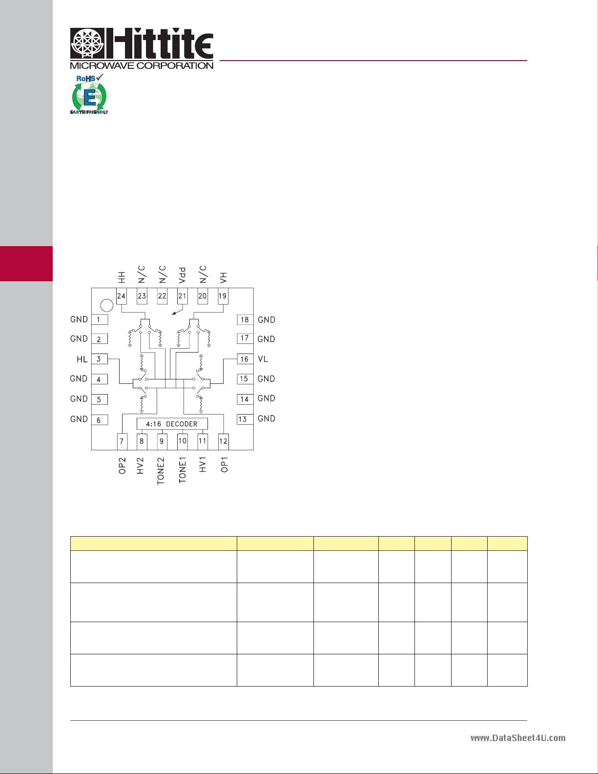
Functional Diagram
Features
High Isolation / Low Insertion Loss
Integrated CMOS Compatible 4 Bit Decoder
Single Positive Supply: Vdd = +5V
QFN Leadless SMT Package, 16 mm
2
4x4 Switch Matrix Using Two ICs
General Description
The HMC596LP4 & HMC596LP4E are low-cost 4x2
switch matrices in leadless QFN 4x4 mm surface
mount packages for use in Satellite / DBS, LNBs
and multiswitches from 200 to 3000 MHz. A positive
voltage controlled 4 bit decoder is integrated on the
switch. The switches may be used in either 75 ohm or
50 ohm systems.
Both switch outputs (OP1 & OP2) can independently
select any of the four inputs (HH, HL, VH, VL) or
simultaneously select the same inputs. Note that the
switch is bi-directional and input/output functionality
may be interchanged. All data presented was
measured in a 50 ohm (input/output) system.
9 - 358
Electrical Specifications, T
Parameter Conditions Frequency Min. Typ. Max. Units
Insertion Loss
Isolation
Return Loss (VL, HL, VH, HH) Input Selected
Return Loss (VL, HL, VH, HH) Input Deselected
= +25° C, Vdd= +5V, 50 Ohm System
A
200 - 950
950 - 2150
2150 - 3000
200 - 950 42 50 dB
950 - 1450 37 45 dB
1450 - 2150
2150 - 3000
200 - 950
950 - 2150
2150 - 3000
200 - 950
950 - 2150
2150 - 3000
25
10
6
6.5
7. 5
43
40
30
7
15
12
17
22
18
7
8
9
For price, delivery, and to place orders, please contact Hittite Microwave Corporation:
20 Alpha Road, Chelmsford, MA 01824 Phone: 978-250-3343 Fax: 978-250 -3373
Order On-line at www.hittite.com
dB
dB
dB
dB
dB
dB
dB
dB
dB
dB
dB
www.DataSheet4U.com
v00.0107
HMC596LP4 / HMC596LP4E
SMT CMOS 4x2 SWITCH
MATRIX, 0.2 - 3.0 GHz
Electrical Specifications, T
Parameter Conditions Frequency Min. Typ. Max. Units
Return Loss (Output OP1/OP2)
Output IP3 200 - 3000 22 27 dBm
Input Power for 1 dB Compression 200 - 3000 18 22 dBm
Switching Speed
tRISE / tFALL (10/90% RF )
tON / tOFF (50% CTL to 10/90% RF)
= +25° C, Vdd= +5V, 50 Ohm System (Continued)
A
200 - 950
950 - 2150
2150 - 3000
9
11
8
13
14
13
6.0
6.5
OP1 Isolation 950 - 1450 MHz OP2 Isolation 950 - 1450 MHz
Min.
Input to
Output State
HL to OP1
VL to OP1
VH to OP1 All States All States 43 >46
HH to OP1 All States All States 37 >40
Interfering
Signal
VL to OP1
All Other States11All Other States384041>43
VH to OP1
All Other States2All Other States394042>43
State
(dB)
Typ .
(dB)
Input to
Output State
HL to OP2
VH to OP2
VL to OP2
HH to OP2 All States All States 38 >41
Interfering
Signal
HH to OP2
All Other States15All Other States384041>43
HL to OP2
All Other States6All Other States374040>43
HL to OP2
All Other States1All Other States374040>43
State
Min.
(dB)
dB
dB
dB
ns
ns
9
Typ .
(dB)
SWITCHES - SMT
Insertion Loss on OP1 Insertion Loss on OP2
0
-1
-2
-3
-4
-5
-6
-7
INSERTION LOSS (dB)
-8
-9
-10
0.2 0.6 1 1.4 1.8 2.2 2.6 3
VL to OP1 (state 1)
VL to OP1 (state 2)
VH to OP1 (state 5)
VH to OP1 (state 6)
HL to OP1 (state 11)
HL to OP1 (state 12)
HH to OP1 (state 15)
HH to OP1 (state 16)
FREQUENCY (GHz)
For price, delivery, and to place orders, please contact Hittite Microwave Corporation:
20 Alpha Road, Chelmsford, MA 01824 Phone: 978-250-3343 Fax: 978-250 -3373
Order On-line at www.hittite.com
0
-1
-2
-3
-4
-5
-6
-7
INSERTION LOSS (dB)
-8
-9
-10
0.2 0.6 1 1.4 1.8 2.2 2.6 3
VL to OP2 (state 1)
VL to OP2 (state 5)
VH to OP2 (state 2)
VH to OP2 (state 6)
HL to OP2 (state 11)
HL to OP2 (state 15)
HH to OP2 (state 12)
HH to OP2 (state 16)
FREQUENCY (GHz)
9 - 359

www.DataSheet4U.com
9
HMC596LP4 / HMC596LP4E
v00.0107
SMT CMOS 4x2 SWITCH
MATRIX, 0.2 - 3.0 GHz
Return Loss Typical Insertion Loss vs. Temperature
0
-5
-10
-15
-20
-25
RETURN LOSS (dB)
-30
-35
0.2 0.6 1 1.4 1.8 2.2 2.6 3
Input RL, Input Selected
Input RL, Input Deselected
Output RL
FREQUENCY (GHz)
Isolation When HL is Connected to OP1* Isolation When VH is Connected to OP1*
0
0
-1
-2
-3
-4
-5
-6
-7
INSERTION LOSS (dB)
-8
-9
-10
0.2 0.6 1 1.4 1.8 2.2 2.6 3
FREQUENCY (GHz)
0
+25C
+85C
-40C
SWITCHES - SMT
-10
-20
-30
-40
ISOLATION (dB)
-50
-60
0.2 0.6 1 1.4 1.8 2.2 2.6 3
HH to OP1 (state 11)
HH to OP1 (state 12)
VH to OP1 (state 10)
VL to OP1 (state 11)
VL to OP1 (state 9)
VH to OP1 (state 11)
FREQUENCY (GHz)
-10
-20
-30
-40
ISOLATION (dB)
-50
-60
0.2 0.6 1 1.4 1.8 2.2 2.6 3
HH to OP1 (state 8)
HL to OP1 (state 6)
HL to OP1 (state 7)
VL to OP1 (state 6)
VL to OP1 (state 5)
HH to OP1 (state 6)
FREQUENCY (GHz)
Isolation When VL is Connected to OP1* Isolation When HH is Connected to OP1*
0
-10
-20
-30
-40
ISOLATION (dB)
-50
HL to OP1 (state 3)
VH to OP1 (state 2)
HH to OP1 (state 1)
HH to OP1 (state 4)
VH to OP1 (state 1)
HL to OP1 (state 1)
0
-10
-20
-30
-40
ISOLATION (dB)
-50
VL to OP1 (state 16)
VH to OP1 (state 16)
VL to OP1 (state 13)
VH to OP1 (state 14)
HL to OP1 (state 16)
HL to OP1 (state 15)
9 - 360
-60
0.2 0.6 1 1.4 1.8 2.2 2.6 3
FREQUENCY (GHz)
-60
* Isolation is recorded above insertion loss & measured at output of switch.
For price, delivery, and to place orders, please contact Hittite Microwave Corporation:
20 Alpha Road, Chelmsford, MA 01824 Phone: 978-250-3343 Fax: 978-250 -3373
Order On-line at www.hittite.com
0.2 0.6 1 1.4 1.8 2.2 2.6 3
FREQUENCY (GHz)

www.DataSheet4U.com
HMC596LP4 / HMC596LP4E
v00.0107
SMT CMOS 4x2 SWITCH
MATRIX, 0.2 - 3.0 GHz
Isolation When HL is Connected to OP2* Isolation When VL is Connected to OP2*
-10
-20
0
HH to OP2 (state 11)
HH to OP2 (state 15)
VH to OP2 (state 7)
VH to OP2 (state 11)
VL to OP2 (state 11)
VL to OP2 (state 3)
-10
-20
0
VH to OP2 (state 1)
VH to OP2 (state 5)
HH to OP2 (state 1)
HH to OP2 (state 13)
HL to OP2 (state 1)
HL to OP2 (state 9)
-30
-40
ISOLATION (dB)
-50
-60
0.2 0.6 1 1.4 1.8 2.2 2.6 3
FREQUENCY (GHz)
-30
-40
ISOLATION (dB)
-50
-60
0.2 0.6 1 1.4 1.8 2.2 2.6 3
FREQUENCY (GHz)
Isolation When VH is Connected to OP2* Isolation When HH is Connected to OP2*
0
-10
-20
-30
-40
ISOLATION (dB)
-50
-60
0.2 0.6 1 1.4 1.8 2.2 2.6 3
HH to OP2 (state 14)
HL to OP2 (state 6)
VL to OP2 (state 2)
VL to OP2 (state 6)
HH to OP2 (state 6)
HL to OP2 (state 10)
FREQUENCY (GHz)
0
-10
-20
-30
-40
ISOLATION (dB)
-50
-60
0.2 0.6 1 1.4 1.8 2.2 2.6 3
HL to OP2 (state 12)
HL to OP2 (state 16)
VH to OP2 (state 8)
VH to OP2 (state 16)
VL to OP2 (state 16)
VL to OP2 (state 4)
FREQUENCY (GHz)
9
SWITCHES - SMT
Output Third Order Intercept Point
Path State
VL to OP1 1 -12 -91 79 27.5
VL to OP2 1 -12 -91 79 27.5
HL to OP1 11 -12 -92 80 28
HL to OP2 11 -12 -91 79 27.5
VH to OP1 6 -12 -90 78 27
VH to OP2 6 -12 -90 78 27
HH to OP1 16 -12 -91 79 27.5
HH to OP2 16 -12 -91 79 27.5
Tes t Co n d iti o ns
Temperature = +25° C
F1 = 2150 (MHz): -12 dBm at the Output
F2 = 2151 (MHz): -12 dBm at the Output
F1 & F2
Pout (dBm)
* Isolation is recorded above insertion loss & measured at output of switch.
For price, delivery, and to place orders, please contact Hittite Microwave Corporation:
20 Alpha Road, Chelmsford, MA 01824 Phone: 978-250-3343 Fax: 978-250 -3373
Order On-line at www.hittite.com
Intermod
Pout (dBm)
Intermodulation
Ratio (dBc)
Vdd = +5V
VCTL Low = 0V, High = +5V
Output
IP3 (dBm)
9 - 361

www.DataSheet4U.com
Truth Table
HMC596LP4 / HMC596LP4E
v00.0107
SMT CMOS 4x2 SWITCH
MATRIX, 0.2 - 3.0 GHz
9
SWITCHES - SMT
Control Input
State HV 1 Tone 1 HV 2 Tone 2 OP1 OP2
1 0 0 0 0 VL VL LOSS ISOL ISOL ISOL LOSS ISOL ISOL ISOL
2 0 0 0 1 VL VH LOSS ISOL ISOL ISOL ISOL ISOL LOSS ISOL
3 0 0 1 0 VL HL LOSS ISOL ISOL ISOL ISOL LOSS ISOL ISOL
4 0 0 1 1 VL HH LOSS ISOL ISOL ISOL ISOL ISOL ISOL LOSS
5 0 1 0 0 VH VL ISOL ISOL LOSS ISOL LOSS ISOL ISOL ISOL
6 0 1 0 1 VH VH ISOL ISOL LOSS ISOL ISOL ISOL LOSS ISOL
7 0 1 1 0 VH HL ISOL ISOL LOSS ISOL ISOL LOSS ISOL ISOL
8 0 1 1 1 VH HH ISOL ISOL LOSS ISOL ISOL ISOL ISOL LOSS
9 1 0 0 0 HL VL ISOL LOSS ISOL ISOL LOSS ISOL ISOL ISOL
10 1 0 0 1 HL VH ISOL LOSS ISOL ISOL ISOL ISOL LOSS ISOL
11 1 0 1 0 HL HL ISOL LOSS ISOL ISOL ISOL LOSS ISOL ISOL
12 1 0 1 1 HL HH ISOL LOSS ISOL ISOL ISOL ISOL ISOL LOSS
13 1 1 0 0 HH VL ISOL ISOL ISOL LOSS LOSS ISOL ISOL ISOL
14 1 1 0 1 HH VH ISOL ISOL ISOL LOSS ISOL ISOL LOSS ISOL
15 1 1 1 0 HH HL ISOL ISOL ISOL LOSS ISOL LOSS ISOL ISOL
16 1 1 1 1 HH HH ISOL ISOL ISOL LOSS ISOL ISOL ISOL LOSS
Control Voltages
Output
to Input State
VL to
OP1
HL to
OP1
Bias Voltage
VH to
OP1
RF Path State
HH to
OP1
VL to
OP2
HL to
OP2
VH to
OP2
HV1, Ton e1, HV2, Ton e2
State Bias Condition
Low (0) 0 to 0.8 Vdc @ 0.5 μA Typical
High (1) +2.0 to +5.0 Vdc @ 0.5 μA Typical
(Vdc)
+5.0 0.2 0.4
Vdd Range = +5.0 Vdc ± 10 %
Vdd
Idd (Typ.)
(mA)
Idd (Max.)
(mA)
HH to
OP2
9 - 362
DC Blocking And Decoupling Capacitors
The HMC596LP4(E) requires DC blocks on all 6 RF ports (OP1, OP2, VL, HL, VH, HH). Characterization on the
HMC596LP4(E) was done using 0402 size 330pF capacitors on all RF ports. A 1,000 pF DC decoupling capacitor
(0603 size) is recommended for the Vdd pin.
For price, delivery, and to place orders, please contact Hittite Microwave Corporation:
20 Alpha Road, Chelmsford, MA 01824 Phone: 978-250-3343 Fax: 978-250 -3373
Order On-line at www.hittite.com

www.DataSheet4U.com
Absolute Maximum Ratings
HMC596LP4 / HMC596LP4E
v00.0107
SMT CMOS 4x2 SWITCH
MATRIX, 0.2 - 3.0 GHz
Bias Voltage Range (Vdd) +8.0 Vdc
Control Voltage Range
(All Logic Lines)
Channel Temperature 150 °C
Thermal Resistance 325 °C/W
Storage Temperature -65 to +150 °C
Operating Temperature - 40 to +85 °C
Maximum Input Power (Each Input) +23 dBm (200 - 2150 MHz)
Vdd + 0.5 to -0.2V Vdc
Outline Drawing
ELECTROSTATIC SENSITIVE DEVICE
OBSERVE HANDLING PRECAUTIONS
9
SWITCHES - SMT
NOTES:
1. LEAD AND GROUND PADDLE MATERIAL: COPPER ALLOY
2. DIMENSIONS ARE IN INCHES [MILLIMETERS].
3. LEAD SPACING TO LERANCE IS NON-CUMU LATIVE.
4. PAD BU RR LENGTH SH ALL BE 0.15mm MAX .
PAD BURR HEIGH T SHALL BE 0. 05mm MA X.
5. PACKAGE WARP SH ALL NOT EXCEED 0.05mm.
6. A LL NC LEADS, GROUN D LEADS AND GROUND PADDLE MUST BE SO LDERED
TO PCB RF GROUND.
7. R EFER TO HITTITE APPLICATION NOTE FOR SUGGESTED PCB LAND PATTERN.
Package Information
Part Number Package Body Material Lead Finish MSL Rating Package Marking
HMC596LP4 Low Stress Injection Molded Plastic Sn/Pb Solder
HMC596LP4E RoHS- compliant Low Stress Injection Molded Plastic 100% matte Sn
[1] Max peak re ow temperature of 235 °C
[2] Max peak re ow temperature of 260 °C
[3] 4-Digit lot number XXXX
For price, delivery, and to place orders, please contact Hittite Microwave Corporation:
20 Alpha Road, Chelmsford, MA 01824 Phone: 978-250-3343 Fax: 978-250 -3373
Order On-line at www.hittite.com
MSL1
MSL1
[1]
[2]
[3]
H596
XXXX
H596
XXXX
9 - 363

www.DataSheet4U.com
HMC596LP4 / HMC596LP4E
v00.0107
SMT CMOS 4x2 SWITCH
MATRIX, 0.2 - 3.0 GHz
Pin Descriptions
Pin Number Function Description Interface Schematic
9
SWITCHES - SMT
1, 2, 4 - 6, 13 - 15,
17, 18
3, 16, 19, 24 HL, VL, VH, HH
7, 12 OP1, OP2
8HV2
9TONE2
10 TONE1
11 HV1
20, 22, 23 N/C Not connected.
21 Vdd Supply Voltag e
GND
Package bottom has exposed metal paddle
that must be connected to PCB RF ground.
Switch RF Input. This pin is DC coupled and should be DC
blocked externally using a series capacitor. Select value
based on lowest frequency of operation.
Switch RF Input. This pin is DC coupled and should be DC
blocked externally using a series capacitor. Select value
based on lowest frequency of operation.
Control Inputs. See truth and control voltage table.
Switch Application Circuit for 4x4 Switch Matrix
9 - 364
The HMC596LP4(E) switch can operate as a 4x4 switch by
connecting the 4 inputs of two switches directly together.
The VL, VH, HL, and HH inputs of the rst switch should be
connected to the second switch, as illustrated.
Mirror image switch performance can be realized by inverting the HV1 & HV2 logic control signals of one of the
HMC596LP4(E) switches.
The input loading impedance of two switches in parallel
should be 31.25 ohms. The output loading impedance on
each output should be 75 ohms. The interconnect RF line
between the switch’s inputs should be an RF trace with a
characteristic impedance of 62.5 ohms. This will allow the
switch to remain matched in all possible switch states.
The HMC596LP4(E) does not provide output to output (OP1
to OP2) isolation. For this reason, it is recommended that
external ampli ers should be used at each output. The
ampli er’s reverse isolation will provide output to output isolation, if this is necessary.
Each HMC596LP4(E) requires DC blocking capacitors on ALL RF input and output ports.
For price, delivery, and to place orders, please contact Hittite Microwave Corporation:
20 Alpha Road, Chelmsford, MA 01824 Phone: 978-250-3343 Fax: 978-250 -3373
Order On-line at www.hittite.com

www.DataSheet4U.com
Evaluation PCB
HMC596LP4 / HMC596LP4E
v00.0107
SMT CMOS 4x2 SWITCH
MATRIX, 0.2 - 3.0 GHz
9
The circuit board used in the nal application should be generated with proper RF circuit design techniques.
Signal lines at the RF port should have 50 ohm impedance and the package ground leads and exposed paddle
should be connected directly to the ground plane similar to that shown above. A generous number of ground vias
should be used to interconnect top/bottom ground planes. The evaluation circuit board shown above is available
from Hittite Microwave Corporation upon request.
List of Materials for Evaluation PCB 104130
Item Description
J2 - J9 PCB Mount SMA RF Connector
J1 DC Connect or
C1 - C8 330 pF Capacitor, 0402 Pkg.
C9 1,000 pF Capacitor, 0603 Pkg.
U1
[2]
PCB
[1] Reference this number when ordering complete evaluation PCB
[2] Circuit Board Material: Rogers 4350
HMC596LP4 / HMC596LP4E
4x2 Switch Matrix
104113 Eval Board
[1]
Multi Pin DC Interface (J1)
Pin Line
1Vdd
2 Tone 1
3GND
4 Tone 2
5GND
6HV1
7N/C
8N/C
9HV2
SWITCHES - SMT
For price, delivery, and to place orders, please contact Hittite Microwave Corporation:
20 Alpha Road, Chelmsford, MA 01824 Phone: 978-250-3343 Fax: 978-250 -3373
Order On-line at www.hittite.com
9 - 365
 Loading...