

Page 1
www.DataSheet4U.com
v02.0107
HMC591LP5 / 591LP5E
GaAs PHEMT MMIC 2 WATT
POWER AMPLIFIER, 6.0 - 9.5 GHz
5
AMPLIFIERS - SMT
Typical Appli cations
The HMC591LP5 / HMC591LP5E is ideal for use as a
power ampli er for:
• Point-to-Point Radios
• Point-to-Multi-Point Radios
• Test Equipment & Sensors
• Military End-Use
• Space
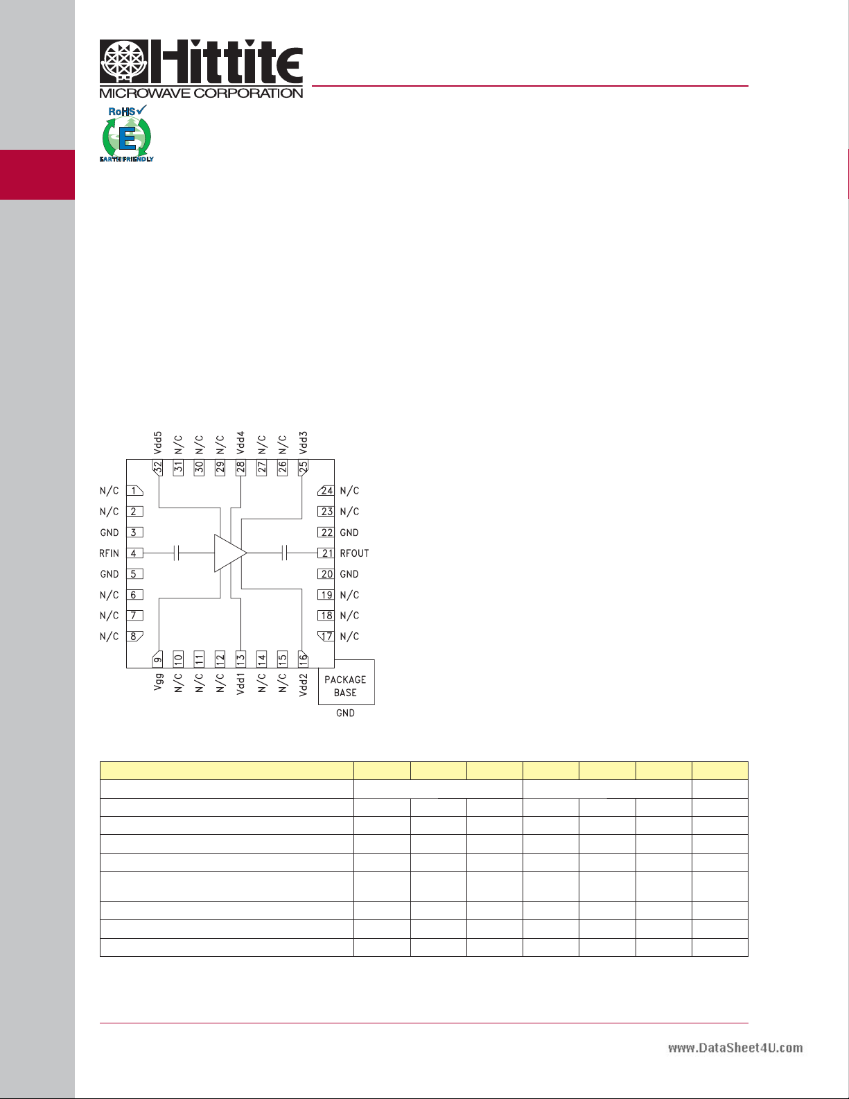
Functional Diagram
Features
Saturated Output Power: +33 dBm @ 20% PAE
Output IP3: +41 dBm
Gain: 18 dB
DC Supply: +7.0 V @ 1340 mA
50 Ohm Matched Input/Output
QFN Leadless SMT Packages, 25 mm
2
General Description
The HMC591LP5 & HMC591LP5E are high dynamic
range GaAs PHEMT MMIC 2 Watt Power Ampli ers
which operate from 6 to 9.5 GHz. The ampli er
provides 18 dB of gain, +33 dBm of saturated power,
and 19% PAE from a +7.0V supply. This 50 Ohm
matched ampli er does not require any external
components and the RF I/Os are DC blocked for robust
operation. For applications which require optimum
OIP3, Idd should be set for 940 mA, to yield +41 dBm
OIP3. For applications which require optimum output P1dB, Idd should be set for 1340 mA, to yield
+33 dBm Output P1dB.
5 - 598
Electrical Specifications, T
Parameter Min. Typ. Max. Min. Typ. Max. Units
Frequency Range 6 - 8 6 - 9.5 GHz
Gain 16 19 15 18 dB
Gain Variation Over Temperature 0.05 0.05 dB/ °C
Input Return Loss 14 12 dB
Output Return Loss 12 10 dB
Output Power for 1 dB
Compression (P1dB)
Saturated Output Power (Psat) 32.5 33 dBm
Output Third Order Intercept (IP3)
Supply Current (Idd) 1340 1340 mA
[1] Adjust Vgg between -2 to 0V to achieve Idd= 1340 mA t ypical.
[2] Measurement taken at 7V @ 940mA, Pin/Tone = -15 dBm
For price, delivery, and to place orders, please contact Hittite Microwave Corporation:
20 Alpha Road, Chelmsford, MA 01824 Phone: 978-250-3343 Fax: 978-250 -3373
[2]
= +25° C, Vdd = +7V, Idd = 1340 mA
A
30 32 30 33 dBm
41 41 d Bm
Order On-line at www.hittite.com
[1]
Page 2
www.DataSheet4U.com
v02.0107
HMC591LP5 / 591LP5E
GaAs PHEMT MMIC 2 WATT
POWER AMPLIFIER, 6.0 - 9.5 GHz
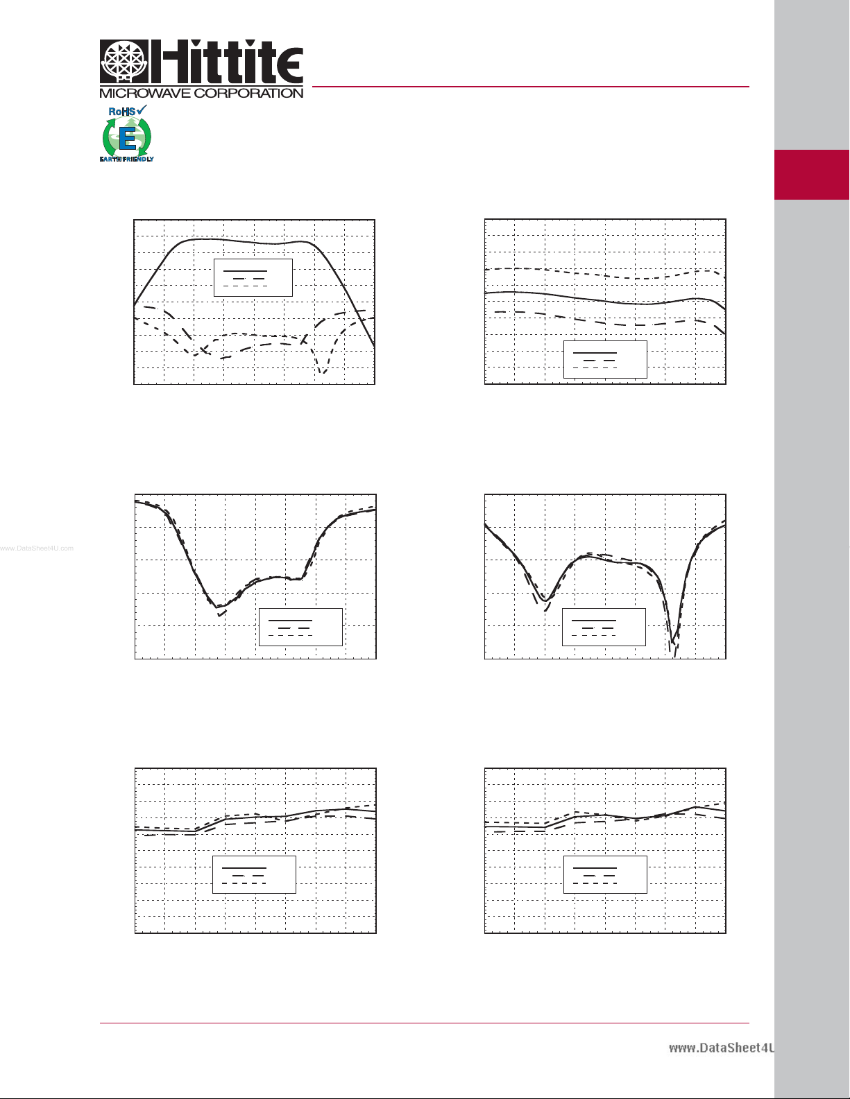
Broadband Gain & Return Loss
25
20
15
10
5
0
-5
RESPONSE (dB)
-10
-15
-20
-25
456789101112
FREQUENCY (GHz)
S21
S11
S22
Gain vs. Temperature
28
26
24
22
20
18
16
GAIN (dB)
14
12
10
8
6 6.5 7 7.5 8 8.5 9 9.5 10
FREQUENCY (GHz)
+25C
+85C
-40C
Input Return Loss vs. Temperature Output Return Loss vs. Temperature
0
-5
-10
0
-5
-10
5
AMPLIFIERS - SMT
-15
RETURN LOSS (dB)
-20
-25
456789101112
FREQUENCY (GHz)
+25C
+85C
-40C
-15
RETURN LOSS (dB)
-20
-25
456789101112
FREQUENCY (GHz)
P1dB vs. Temperature Psat vs. Temperature
36
35
34
33
32
31
30
P1dB (dBm)
29
28
27
26
6 6.5 7 7.5 8 8.5 9 9.5 10
FREQUENCY (GHz)
+25C
+85C
-40C
36
35
34
33
32
31
30
Psat (dBm)
29
28
27
26
6 6.5 7 7.5 8 8.5 9 9.5 10
FREQUENCY (GHz)
+25C
+85C
-40C
+25C
+85C
-40C
For price, delivery, and to place orders, please contact Hittite Microwave Corporation:
20 Alpha Road, Chelmsford, MA 01824 Phone: 978-250-3343 Fax: 978-250 -3373
Order On-line at www.hittite.com
5 - 599
Page 3
www.DataSheet4U.com
v02.0107
HMC591LP5 / 591LP5E
GaAs PHEMT MMIC 2 WATT
POWER AMPLIFIER, 6.0 - 9.5 GHz
5
AMPLIFIERS - SMT
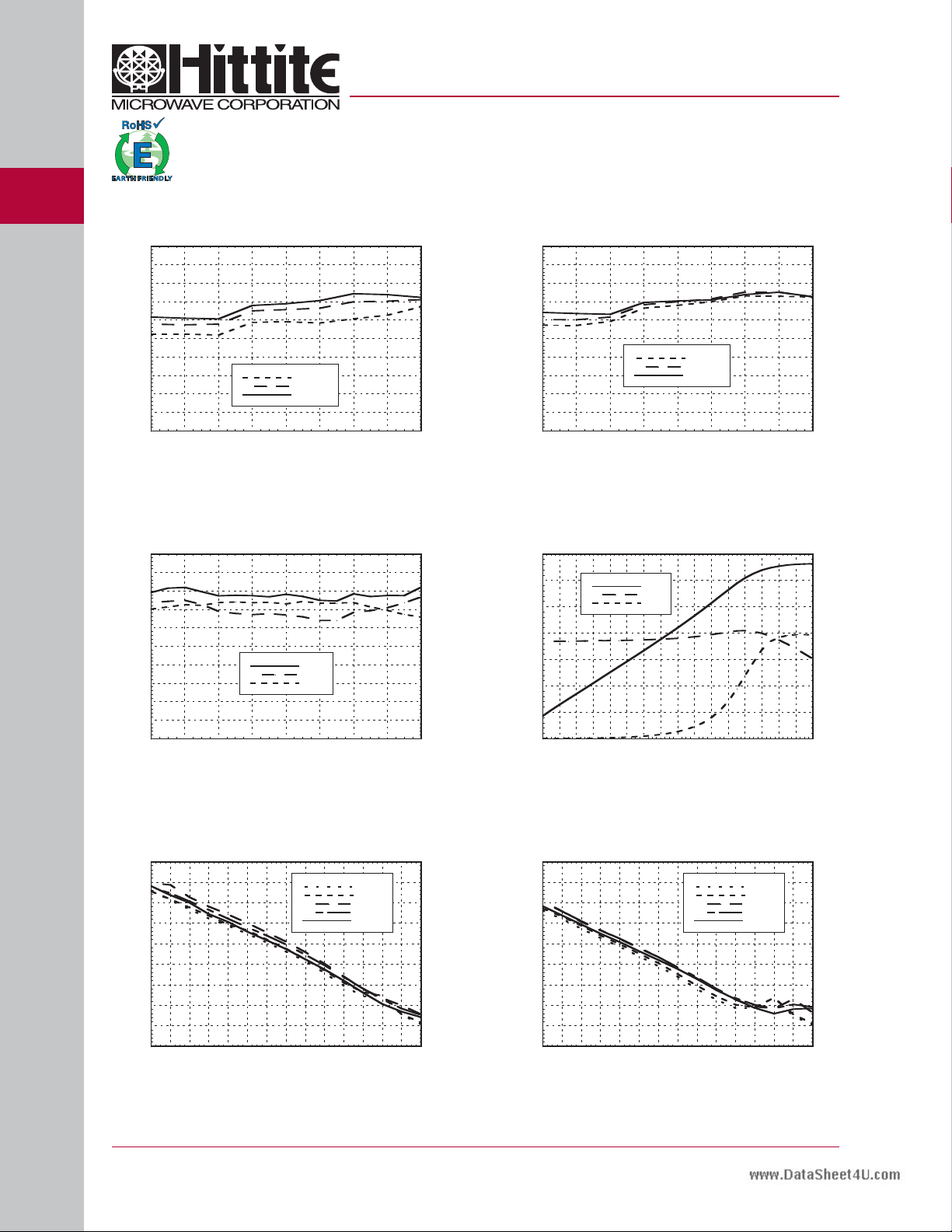
36
35
34
33
32
31
30
P1dB (dBm)
29
28
27
26
6 6.5 7 7.5 8 8.5 9 9.5 10
FREQUENCY (GHz)
940 mA
1140 mA
1340 mA
Output IP3 vs. Temperature
7V @ 940 mA, Pin/Tone = -15 dBm
46
44
42
40
38
36
34
OIP3 (dBm)
32
30
28
26
6 6.5 7 7.5 8 8.5 9 9.5 10
FREQUENCY (GHz)
+25C
+85C
-40C
Psat vs. CurrentP1dB vs. Current
36
35
34
33
32
31
30
Psat (dBm)
29
28
27
26
6 6.5 7 7.5 8 8.5 9 9.5 10
FREQUENCY (GHz)
940 mA
1140 mA
1340 mA
Power Compression @ 8 GHz,
7V @ 1340 mA
35
30
25
20
15
10
Pout(dBm), GAIN (dB), PAE(%)
5
0
-14 -12 -10 -8 -6 -4 -2 0 2 4 6 8 10 12 14 16 18
Pout
Gain
PAE
INPUT POWER (dBm)
5 - 600
Output IM3, 7V @ 940 mA Output IM3, 7V @ 1340 mA
100
90
80
70
60
50
IM3 (dBc)
40
30
20
10
-20 -18 -16 -14 -12 -10 -8 -6 -4 -2 0 2 4 6 8
Pin/Tone (dBm)
6 GHz
7 GHz
8 GHz
9 GHz
10 GHz
For price, delivery, and to place orders, please contact Hittite Microwave Corporation:
20 Alpha Road, Chelmsford, MA 01824 Phone: 978-250-3343 Fax: 978-250 -3373
Order On-line at www.hittite.com
100
90
80
70
60
50
IM3 (dBc)
40
30
20
10
-20 -18 -16 -14 -12 -10 -8 -6 -4 -2 0 2 4 6 8
Pin/Tone (dBm)
6 GHz
7 GHz
8 GHz
9 GHz
10 GHz
Page 4

www.DataSheet4U.com
v02.0107
HMC591LP5 / 591LP5E
GaAs PHEMT MMIC 2 WATT
POWER AMPLIFIER, 6.0 - 9.5 GHz
36
34
32
30
28
26
24
22
20
18
GAIN (dB), P1dB (dBm), Psat(dBm)
16
940 1140 1340
Idd SUPPLY CURRENT (mA)
Gain
P1dB
Psat
Reverse Isolation
vs. Temperature, 7V @ 1340 mA
0
-10
-20
-30
-40
-50
ISOLATION (dB)
-60
-70
-80
6 6.5 7 7.5 8 8.5 9 9.5 10
FREQUENCY (GHz)
+25C
+85C
-40C
Gain & Power vs. Supply Voltage @ 8 GHzGain & Power vs. Supply Current @ 8 GHz
36
34
32
30
28
26
24
22
20
18
GAIN (dB), P1dB (dBm), Psat(dBm)
16
6.5 7 7.5
Vdd SUPPLY VOLTAGE (Vdc)
Gain
P1dB
Psat
Power Dissipation
10
9.5
9
8.5
8
7.5
7
POWER DISSIPATION (W)
6.5
6
-14 -12 -10 -8 -6 -4 -2 0 2 4 6 8 10 12 14
6 GHz
7 GHz
8 GHz
9 GHz
10 GHz
INPUT POWER (dBm)
5
AMPLIFIERS - SMT
Absolute Maximum Ratings
Drain Bias Voltage (Vdd) +8 Vdc
Gate Bias Voltage (Vgg) -2.0 to 0 Vdc
RF Input Power (RFin)(Vdd = +7.0 Vdc) +15 dBm
Channel Temperature 175 °C
Continuous Pdiss (T= 75 °C)
(derate 104.3 mW/°C above 75 °C)
Thermal Resistance
(channel to package bottom)
Storage Temperature -65 to +150 °C
Operating Temperature -40 to +85 °C
For price, delivery, and to place orders, please contact Hittite Microwave Corporation:
20 Alpha Road, Chelmsford, MA 01824 Phone: 978-250-3343 Fax: 978-250 -3373
10.43 W
9.59 °C/ W
Order On-line at www.hittite.com
Typical Supply Current vs. Vdd
Vdd (V) Idd (mA)
+6.5 1350
+7.0 1340
+7.5 1330
Note: Amplifier will operate over full voltage ranges shown
above Vgg adjusted to achieve Idd = 1340 mA at +7.0V
ELECTROSTATIC SENSITIVE DEVICE
OBSERVE HANDLING PRECAUTIONS
5 - 601
Page 5

www.DataSheet4U.com
v02.0107
HMC591LP5 / 591LP5E
GaAs PHEMT MMIC 2 WATT
POWER AMPLIFIER, 6.0 - 9.5 GHz
5
AMPLIFIERS - SMT
Outline Drawing
NOTES:
1. LEADFRAME MATERIAL: COPPER ALLOY
2. DIMENSIONS ARE IN INCHES [MILLIMETERS]
3. LEAD SPACING TOLERANCE IS NON -CUM ULATIVE
4. PAD BURR LENGTH S HALL BE 0.15mm MA XIMUM.
PAD BURR HEIGH T SHALL BE 0.05mm MA XIMUM .
5. PACKAGE WARP SH ALL NOT EXCEED 0.05mm.
6. ALL GROUND LEADS AND GROUND PADDLE MUST B E
SOLDERED TO PCB RF GROU ND.
7. REFER TO HITTITE APPLICATION NOTE FOR SUGGESTED
LAND PATTERN.
Package Information
Part Number Package Body Material Lead Finish MSL Rating Package Marking
HMC591LP5 Low Stress Injection Molded Plastic Sn/Pb Solder
HMC591LP5E RoHS- compliant Low Stress Injection Molded Plastic 100% matte Sn
[1] Max peak re ow temperature of 235 °C
[2] Max peak re ow temperature of 260 °C
[3] 4-Digit lot number XXXX
MSL1
MSL1
[1]
[2]
[3]
H591
XXXX
H591
XXXX
5 - 602
For price, delivery, and to place orders, please contact Hittite Microwave Corporation:
20 Alpha Road, Chelmsford, MA 01824 Phone: 978-250-3343 Fax: 978-250 -3373
Order On-line at www.hittite.com
Page 6

www.DataSheet4U.com
v02.0107
HMC591LP5 / 591LP5E
GaAs PHEMT MMIC 2 WATT
POWER AMPLIFIER, 6.0 - 9.5 GHz
Pad Descriptions
Pad Number Function Description Interface Schematic
1, 2, 6 - 8,
10 - 12, 14, 15,
17 - 19, 23, 24,
26, 27, 29 - 31
3, 5, 20, 22 GND
4RFIN
9Vgg
13, 16, 25, 28, 32 Vdd 1-5
21 RFOUT
N/C Not connected.
Package bottom has an exposed metal paddle
that must be connected to RF/DC ground.
This pad is AC coupled and
matched to 50 Ohms.
Gate control for ampli er. Adjust to achieve Idd of 1340 mA.
Please follow “MMIC Ampli er Biasing Procedure”
Application Note. External bypass capacitors of
100 pF and 2.2 μF are required.
Power Supply Voltage for the ampli er. External bypass
capacitors of 100 pF and 2.2 μF are required.
This pad is AC coupled and
matched to 50 Ohms.
5
AMPLIFIERS - SMT
For price, delivery, and to place orders, please contact Hittite Microwave Corporation:
20 Alpha Road, Chelmsford, MA 01824 Phone: 978-250-3343 Fax: 978-250 -3373
Order On-line at www.hittite.com
5 - 603
Page 7

www.DataSheet4U.com
v02.0107
HMC591LP5 / 591LP5E
GaAs PHEMT MMIC 2 WATT
POWER AMPLIFIER, 6.0 - 9.5 GHz
5
Application Circuit
Component Value
C1 - C6 100pF
C7 - C12 2.2μF
AMPLIFIERS - SMT
5 - 604
For price, delivery, and to place orders, please contact Hittite Microwave Corporation:
20 Alpha Road, Chelmsford, MA 01824 Phone: 978-250-3343 Fax: 978-250 -3373
Order On-line at www.hittite.com
Page 8

www.DataSheet4U.com
v02.0107
HMC591LP5 / 591LP5E
GaAs PHEMT MMIC 2 WATT
POWER AMPLIFIER, 6.0 - 9.5 GHz
Evaluation PCB
5
AMPLIFIERS - SMT
List of Materials for Evaluation PCB 108190
Item Description
J1 - J2 PCB Mount SMA Connector
J3 - J4 DC Pin
C1 - C6 100pF Capacitor, 0402 Pkg.
C7 - C12 2.2 μF Capacitor, 1206 Pkg
U1 HMC591LP5 / HMC591LP5E
[2]
PCB
[1] Reference this number when ordering complete evaluation PCB
[2] Circuit Board Material: Rogers 4350
For price, delivery, and to place orders, please contact Hittite Microwave Corporation:
109001 Evaluation PCB
20 Alpha Road, Chelmsford, MA 01824 Phone: 978-250-3343 Fax: 978-250 -3373
Order On-line at www.hittite.com
[1]
The circuit board used in the nal application
should use RF circuit design techniques. Signal
lines should have 50 ohm impedance while the
package ground leads and package bottom should
be connected directly to the ground plane similar to
that shown. A suf cient number of via holes should
be used to connect the top and bottom ground
planes. The evaluation board should be mounted
to an appropriate heat sink. The evaluation circuit
board shown is available from Hittite upon request.
5 - 605
 Loading...