

Page 1
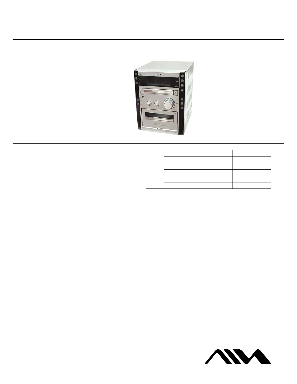
CX-LFA500
SERVICE MANUAL
Ver. 1.4 2005. 10
CX-LFA500 is the Amplifier, CD player, Tape
Deck and Tuner section in XR-FA500.
CD
Section
TAPE
Section
AEP Model
UK Model
E Model
Australian Model
Model Name Using Similar Mechanism NEW
CD Mechanism Type CDM55A-K6BD44B
Base Unit Name BU-K1BD44B
Optical Pick-up Name KSM-213D
Model Name Using Similar Mechanism NEW
Tape Transport Mechanism Type CMAL1Z222B
SPECIFICATIONS
TUNER
FM tuning range 87.5 MHz to 108 MHz
(50 kHz step)
FM usable sensitivity (IHF) 16.8 dBf
FM antenna terminal 75 (unbalanced)
AM tuning range
European model: 531-1,602 kHz
(with the tuning interval set at 9 kHz)
Other models: 530-1,710 kHz
(with the tuning interval set at 10 kHz)
531-1,602 kHz
(with the tuning interval set at 9 kHz)
AM usable sensitivity 350 μV/m
AM antenna Loop antenna
AMPLIFIER
Power output Rated: 16 W + 16 W(6 ohms, T.H.D.
1 %, 1 kHz/DIN 45500)
Reference: 20 W + 20 W(6 ohms,
T.H.D. 10 %, 1 kHz/DIN 45324)
MUSIC POWER
40 W + 40 W
Input AUX IN: 500 mV
Outputs SPEAKERS: 6 ohms or more
PHONES: 32 ohms or more
CASSETTE DECK
Track format 4 tracks, 2 channels stereo
Frequency response 50 Hz – 10000 Hz
Recording system AC bias
Heads Recording/playback × 1, erase × 1
CD PLAYER
Laser Semiconductor laser ( = 780 nm)
Emission duration: continuous
D/A converter 1 bit dual
Signal-to-noise ratio 80 dB (1 kHz, 0 dB)
Wow and flutter Unmeasurable
— Continued on next page —
MICRO HI-FI COMPONENT SYSTEM
9-877-166-05
2005J16-1
© 2005.10
Sony Corporation
Personal Audio Division
Published by Sony Engineering Corporation
Page 2

CX-LFA500
Ver 1.2 2003.11
TABLE OF CONTENTS
GENERAL
Power requirements
European model:
Singaporeand
Australian models:
Korean model:
Taiwan model:
Other models:
Power consumption
European model:
Other models:
Power consumption in standby mode
Dimensions (w/h/d) Approx. 190 × 250 ×
Mass Approx. 3.7 kg
Supplied accessories: FM antenna (1)
Specifications and external appearance are subject to change
without notice.
230 V AC, 50/60 Hz
220 V + 240 V AC, 50/60 Hz
220-240 V AC, 50/60 Hz
220 V AC, 60 Hz
110-120 V AC, 50/60 Hz
110-120 V/220-240 V AC, 50/60 Hz
52W
60W
with ECO mode on: 0.3 W
with ECO mode off: 10 W
284 mm
AM antenna (1)
Speaker cords (2)
Remote commander (1)
Batteries (2)
1. SERVICING NOTES ······················································· 3
2. GENERAL ·········································································· 5
3. DISASSEMBLY
3-1. Top Cabinet, Rear Panel·················································· 7
3-2. Front Panel Assy ····························································· 8
3-3. CONTROL Board, Single Cassette Mechanism············· 8
3-4. CD Mechanism Deck (CDM55A-K6BD44B)················ 9
3-5. MAIN Board, POWER Board ········································9
3-6. LOADING Board·························································· 10
3-7. CD Board ······································································ 10
3-8. Tray (CDM55D) ··························································· 11
3-9. Optical Pick-up (KSM-213D), Holder (C213) ············· 11
4. MECHANICAL ADJUSTMENTS ····························· 13
5. ELECTRICAL ADJUSTMENTS ······························· 14
6. DIAGRAMS······································································ 17
6-1. Block Diagram – CD Section – ··································· 18
6-2. Block Diagram – Main Section – ································ 19
6-3. Printed Wiring Board – CD Section – ························· 20
6-4. Schematic Diagram – CD Section – ···························· 21
6-5. Printed Wiring Boards – Main Section – ····················· 22
6-6. Schematic Diagram – Main Section – ························· 23
6-7. Printed Wiring Board – Control Section – ··················· 24
6-8. Schematic Diagram – Control Section –······················ 25
6-9. Printed Wiring Board – Power Section – ····················· 26
6-10. Schematic Diagram – Power Section –······················ 26
6-11. IC Pin Function Description ······································· 30
7. EXPLODED VIEWS
7-1. Overall Section ····························································· 32
7-2. Front Section································································· 33
7-3. Chassis Section ····························································· 34
7-4. CD Mechanism Deck Section······································· 35
7-5. Optical Pick-up Section (KSM-213D)·························· 36
8. ELECTRICAL PARTS LIST······································· 37
2
Page 3
SECTION 1
SERVICING NOTES
CX-LFA500
Notes on chip component replacement
• Never reuse a disconnected chip component.
• Notice that the minus side of a tantalum capacitor may be damaged by heat.
Flexible Circuit Board Repairing
• Keep the temperature of the soldering iron around 270 ˚C during
repairing.
• Do not touch the soldering iron on the same conductor of the
circuit board (within 3 times).
• Be careful not to apply force on the conductor when soldering or
unsoldering.
CAUTION
Use of controls or adjustments or performance of procedures
other than those specified herein may result in hazardous
radiation exposure.
This appliance is classified as a CLASS 1 LASER product.
The CLASS 1 LASER PRODUCT MARKING is located on
the exterior.
Laser component in this product is capable of emitting radiation
exceeding the limit for Class 1.
NOTES ON HANDLING THE OPTICAL PICK-UP
BLOCK OR BASE UNIT
The laser diode in the optical pick-up block may suffer electrostatic
break-down because of the potential difference generated by the
charged electrostatic load, etc. on clothing and the human body.
During repair, pay attention to electrostatic break-down and also
use the procedure in the printed matter which is included in the
repair parts.
The flexible board is easily damaged and should be handled with
care.
SAFETY-RELATED COMPONENT WARNING!!
COMPONENTS IDENTIFIED BY MARK 0 OR DOTTED LINE WITH
MARK 0 ON THE SCHEMATIC DIAGRAMS AND IN THE PARTS
LIST ARE CRITICAL TO SAFE OPERATION. REPLACE THESE
COMPONENTS WITH SONY PARTS WHOSE PART NUMBERS
APPEAR AS SHOWN IN THIS MANUAL OR IN SUPPLEMENTS
PUBLISHED BY SONY .
NOTES ON LASER DIODE EMISSION CHECK
The laser beam on this model is concentrated so as to be focused on
the disc reflective surface by the objective lens in the optical pickup block. Therefore, when checking the laser diode emission,
observe from more than 30 cm away from the objective lens.
LASER DIODE AND FOCUS SEARCH OPERATION
CHECK
Carry out the “S curve check” in “CD section adjustment” and check
that the S curve waveforms is output three times.
3
Page 4
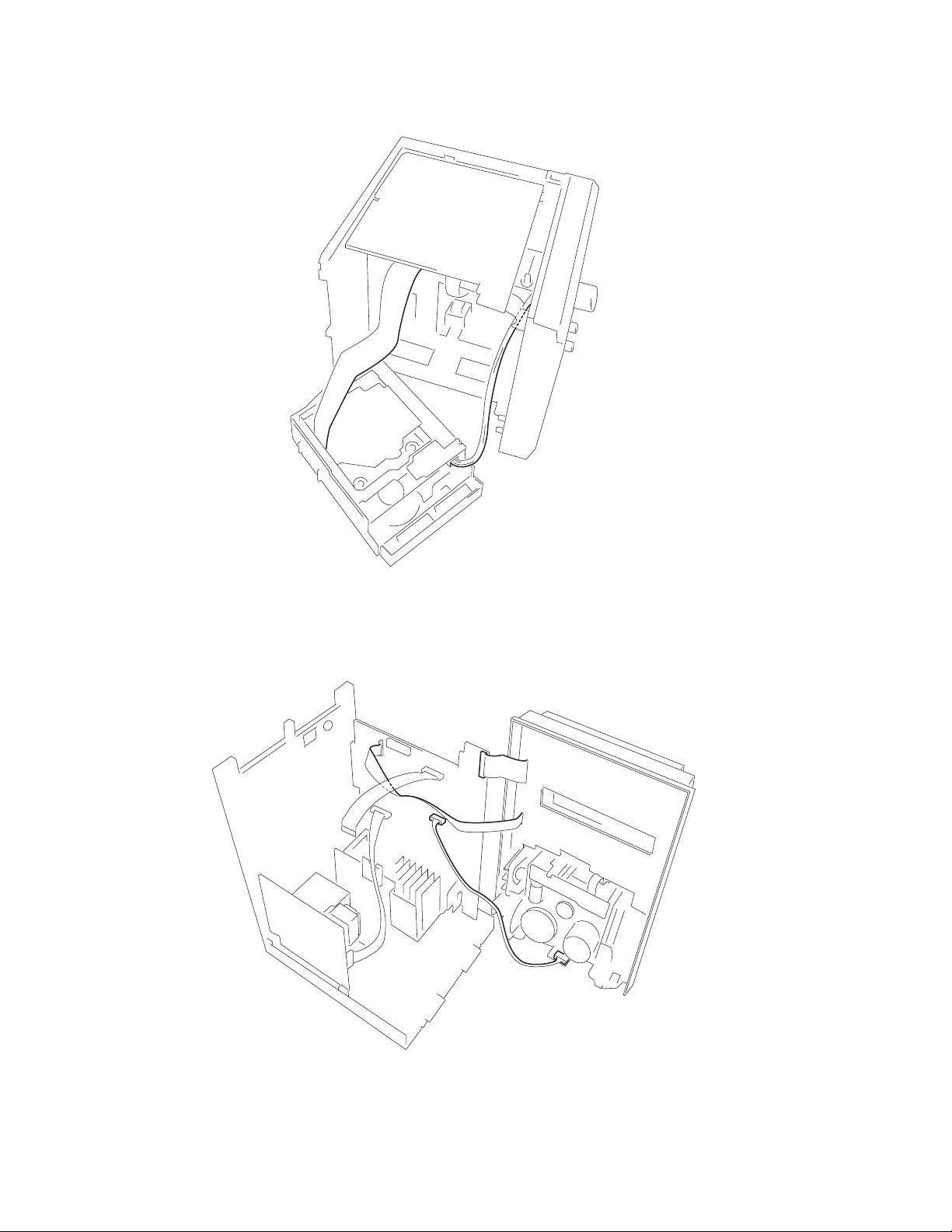
CX-LFA500
Service Position of the CD Mechanism Deck
Service Position of the Tape Cassette Mechanism Deck
4
Page 5
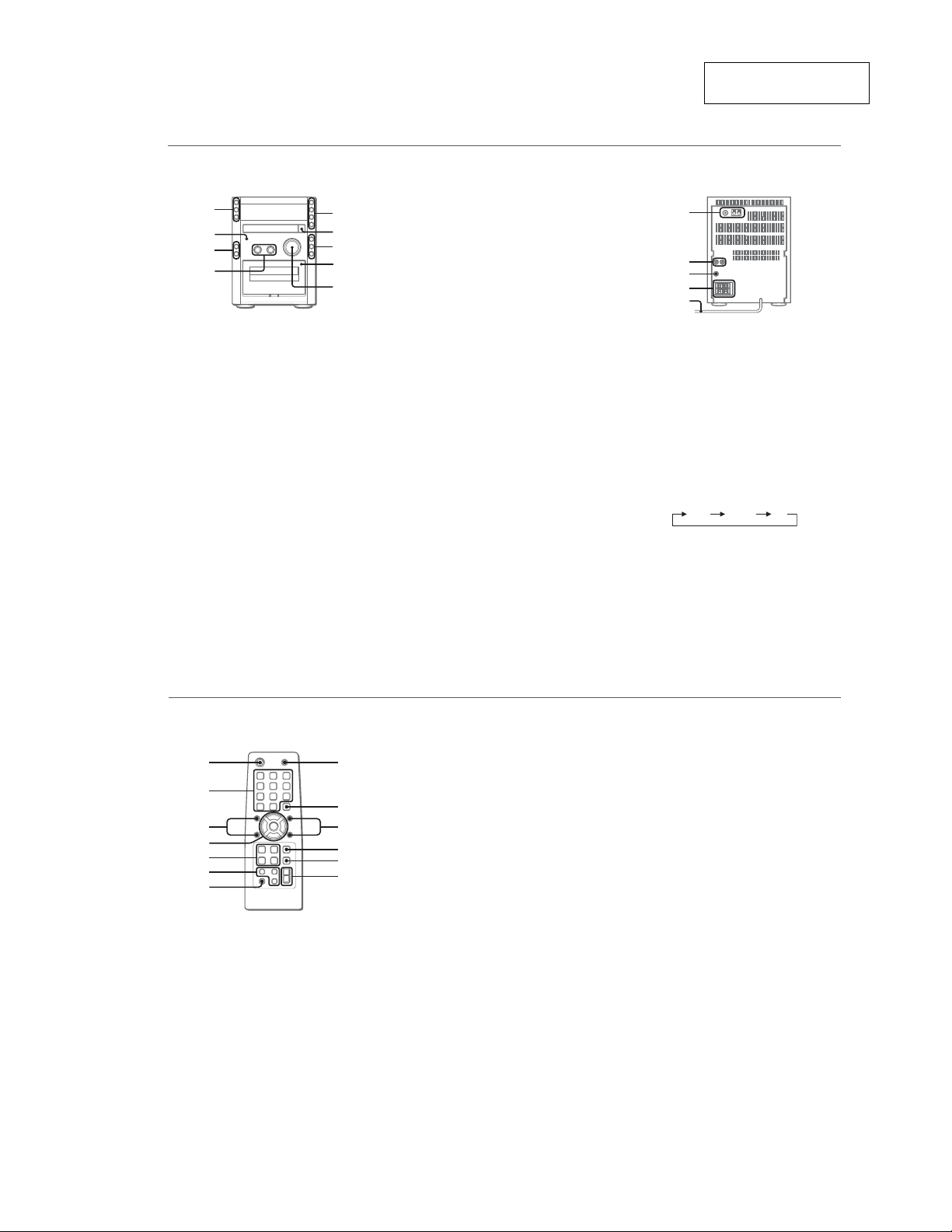
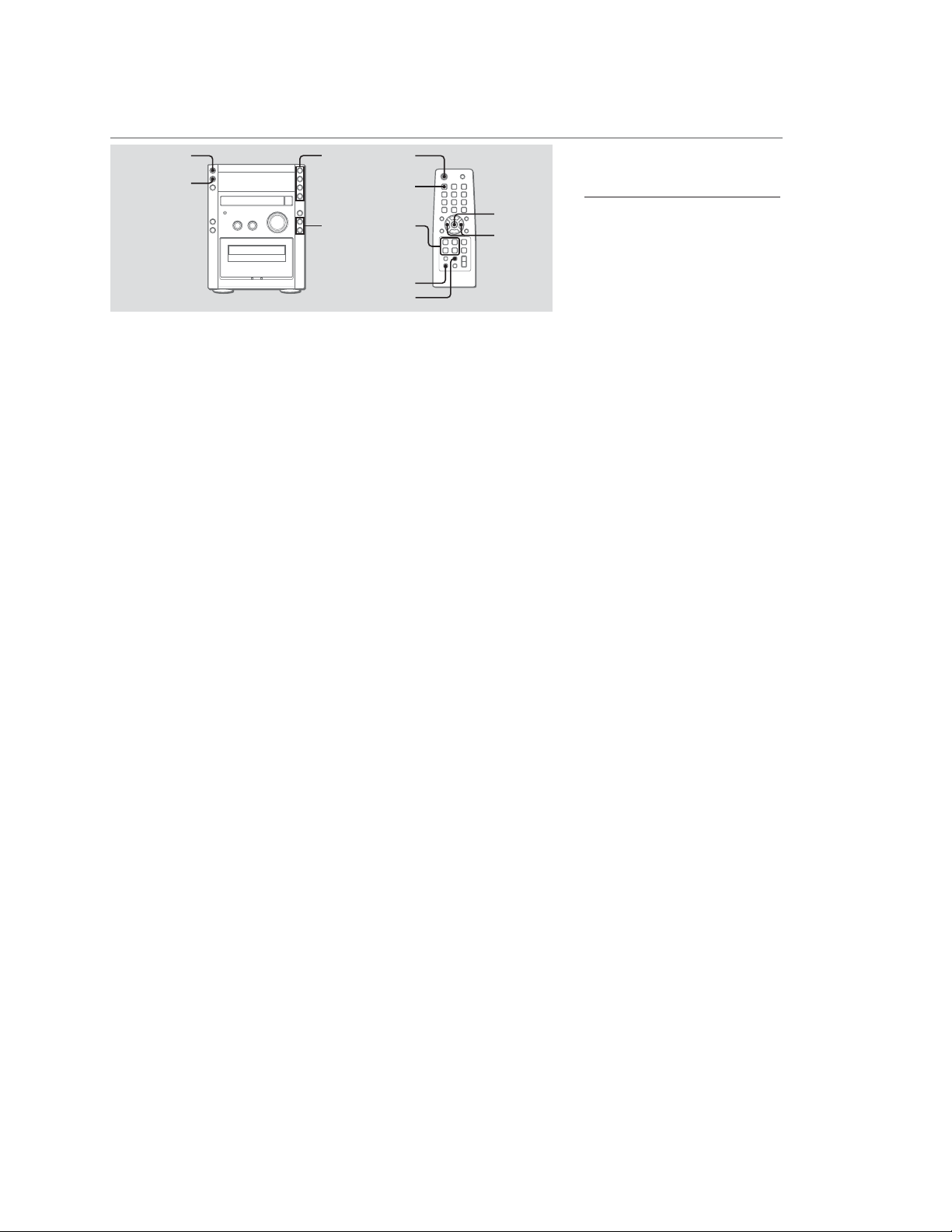
PARTS AND CONTROLS
Main unit: front
Refer to the pages indicated in parentheses for details.
1
2
3
4
1 POWER 6STANDBY/ON (7)
Switches the unit on and off (standby).
ECO (7)
Sets the ECO mode on or off.
RDS (10-12)
Activates RDS features.
2 PHONES jack
Plug in optional headphones set with a stereo mini plug
(ø3.5 mm). Speaker output is cancelled.
3 SYNCHRO REC (15)
Starts recording and CD play simultaneously.
wREC START/REC PAUSE (15)
Starts and pauses recording.
4 BASS (13)
Adjusts the bass level.
TREBLE (13)
Adjusts the treble level.
5
6
7
8
9
SECTION 2
GENERAL
5 ECD (7-9)
Starts and pauses CD play.
TUNER/BAND (7, 10)
Selects tuner function and the tuner band.
dTAPE (REC MUTING) (7, 14, 15)
Starts playback and changes the playback side.
Also used to enter 4-second blank spaces during
recording.
AUX (7)
Selects the function of external equipment connected to
AUX IN jacks.
6 zOPEN/CLOSE (8)
Opens or closes the disc compartment.
7 sSTOP (8, 9, 14, 15)
CD and Tape: stops playback.
f/r-, +t/g (8, 10, 12-14, 16,
17)
CD: skips to a previous or a succeeding track when
pressed, searches a track in fast forward or reverse
playback when held down.
Tape: rewinds or fast forwards the tape.
Tuner: manually tunes up or down within the band.
8 zPUSH EJECT (14, 15)
Opens or closes the cassette holder.
9 VOLUME (13, 16)
Adjusts the volume.
CX-LFA500
This section is extracted
from instruction manual.
Main unit: rear
Refer to the pages indicated in parentheses for details.
1
2
3
4
5
1 AM LOOP terminal and FM 75 Ω terminal
(4)
Plug in the supplied AM and FM antennas.
2 AUX IN jacks
Accept analogue sound signals from external equipment.
Connect external equipment using an optional connecting
cable with RCA phono plugs (red plug to R jack, white
plug to L jack). Refer also to the operating instructions
for your equip
To switch function to external input, press AUX.
To change a source name in the display of the
AUX function.
Hold down AUX and press POWER while the power is
on.
3 SUB WOOFER3 jack
Connect optional powered sub woofer with a built-in
amplifier to the jack.
4 SPEAKERS3 terminals (4)
Connect the speaker cords of the supplied speakers.
5 AC power cord (4)
ment.
AUX VIDEO TV
5
Remote commander
Refer to the pages indicated in parentheses for details.
1
2
3
4
5
6
7
Buttons with the same or similar names on the main unit
basically have the same function.
1 POWER (7)
2 1–10/0, >10 (8, 10)
CD: selects a track of the specified number.
Tuner: tunes in the station with the specified preset
number.
The numbered buttons take on these functions when pressed with
SHIFT held down
CLOCK (7)
Selects clock mode.
TIMER (16)
Selects timer mode.
TUNER MODE (13)
Switches between stereo or monaural FM reception.
:
8
9
0
!
@
#
REV MODE (14, 15)
Selects a reverse mode.
3 SHUFFLE/PROGRAM (8, 9)
Selects shuffle or programmed CD playback mode.
REPEAT (8)
Selects repeat CD playback mode.
4 PRESETN,M (10)
f/r,t/g (8, 10, 12-14, 16, 17)
ENTER (7, 10, 16, 17)
Determines the mode.
Stores the received station to preset.
5 ECD (7-9)
TUNER/BAND (7, 10)
dTAPE (7, 12)
AUX (7)
6 DISPLAY (8)
Changes the display in CD playback mode.
DIMMER (7)
Adjusts the display window brightness.
SLEEP (16)
Selects sleep-timer mode.
7 SHIFT
Hold down when pressing a numbered button to change
its function to that printed above the number.
8 MUTING (13)
To turn off the sound temporarily.
9 CLEAR (9, 10, 17)
CD: Clears a CD program
Tuner: Clears a preset station.
0 TREBLE (13)
BASS (13)
! s (8, 9, 14, 15)
@ FUNCTION (15)
Switches the active function among TAPE, TUNER, AUX
(VIDEO or TV) and CD.
# VOLUME +,- (13)
6
5
Page 6
CX-LFA500
ADJUSTMENTS BEFORE OPERATION
POWER
6STANDBY/ON
ECO
Power
Turning the unit on
Press POWER 6STANDBY/ON (POWER on the remote ).
Alternatively, press d TA PE, TUNER/BAND, AUX or
ECD. Playback will start automatically if a disc or tape is
loaded.
Turning the unit off
Press POWER 6STAN
The unit goes into standby.
DBY/ON again.
Dimmer
The display window brightness can be selected.
Press DIMMER on the remote repeatedly.
Each press of the button changes the following three levels:
"DIMMER 1", "DIMMER 2" and "DIMMER 0".
"DIMMER 0" is brightest.
ECD,
TUNER/
BAND,
dTAPE,
AUX
f,g
ECO mode
Reduces power consumption in standby mode with the following
operations.
Press ECO.
Each press of the button changes the mode as follows;
ECO ON: Power economizing mode is activated.
When the unit turns off, everything in the display disappears
and only the red indicator above POWER lights to show that
the power is being supplied.
ECO OFF
When the unit turns off, the clock display appears.
Initial mode is ECO OFF.
Standby power consumption
ECO ON: 0.3 W
ECO OFF: 10 W
POWER
CLOCK
ECD,
TUNER/
BAND,
dTAPE,
AUX
SHIFT
DIMMER
: Power economizing mode is cancelled.
ENTER
f,g
Setting the clock
1
In stop mode, hold down SHIFT and press CLOCK
on the remote.
Go to step 3 when the hour of the clock display flashes.
2
Within 6 seconds, press ENTER.
The hour flashes in the display.
3
Press f or g to set the hour, then press
ENTER.
4
Press f or g to set the minute.
Each press changes the time in 1-minute steps.
5
Press ENTER.
The time display stops flashing and the clock starts from
00 seconds.
To display the time while the power is on
Hold down SHIFT and press CLOCK on the remote.
The time will be displayed for 6 seconds.
Tip:
''AM 12:00" indicates midnight and "PM12:00" noon.
If "- -:- -" appears when the unit is turned off
There has been a power interruption. Reset the clock.
7
6
Page 7
• This set can be disassembled in the order shown below.
)
)
SET
TOP CABINET,
REAR PANEL
FRONT PANEL ASSY
SECTION 3
DISASSEMBLY
CX-LFA500
Ver 1.2 2003.11
CD MECHANISM DECK
(CDM55A-K6BD44B)
MAIN BOARD,
POWER BOARD
Note: Follow the disassembly procedure in the numerical order given.
CONTROL BOARD,
SINGLE CASSETTE MECHANISM
LOADING BOARD CD BOARD TRAY (CDM55D)
3-1. Top Cabinet, Rear Panel
5
2
three s
(+KTP 3
crews
×
12)
top cabinet
a
3
six s
crews
(+BVTP 3
6
w
ire (flat type)
15p
OPTICAL PICK-UP
(KSM-213D),
HOLDER (C213)
×
10)
qa
rear panel
a
9
three s
(+BVTP 3
7
(+BVTP 3
two s
crews
×
crews
10)
×
10
4
1
three s
(+KTP 3
crews
×
12)
b
q;
tuner (FM/AM)
b
8
three s
(+BVTP 3
crews
×
10
7
Page 8
CX-LFA500
)
)
3-2. Front Panel Assy
4
w
ire (flat type) 25p (CN302)
8
front panel assy
5
connector 5p (CN1)
6
connector 6p
3
w
ire (flat type) 12p (CN305)
2
four s
crews
(+BVTP 3
×
10
1
two s
crews
(+KTP 3
×
12)
3-3. CONTROL Board, Single Cassette Mechanism
1
twelve s
5
CONTROL
4
w
ire (flat type) 8p (CN603)
board
7
connector 5p (CN201)
crews (+BVTP 3
2
×
10)
w
ire (flat type) 25p (CN601)
3
w
ire (flat type) 12p (CN602)
6
four s
crews (+BVTP 3
7
single cassette mechanism
(CMAL1Z222B)
×
10
8
Page 9
3-4. CD Mechanism Dec k (CDM55A-K6BD44B)
)
6
CD door assy
7
CD mechanism deck
(CDM55A-K6BD44B)
4
5
CD holder
3
s
crew (+BVTP 3
2
w
×
10)
ire (flat type) 21p (CN303)
CX-LFA500
3-5. MAIN Board, POWER Board
7
four s
crews
9
POWER board
(+BVTP 3
×
10)
8
power transformer
1
connector 7p (CN801)
4
six s
crews
(+BVTP 3
6
MAIN board
3
(+BVTP 3
1
s
crew (+BVTP 3
×
10)
two s
crews
×
10)
×
10)
5
heat sink assy
2
two s
crews (+BVTP 3
×
10
9
Page 10
CX-LFA500
p
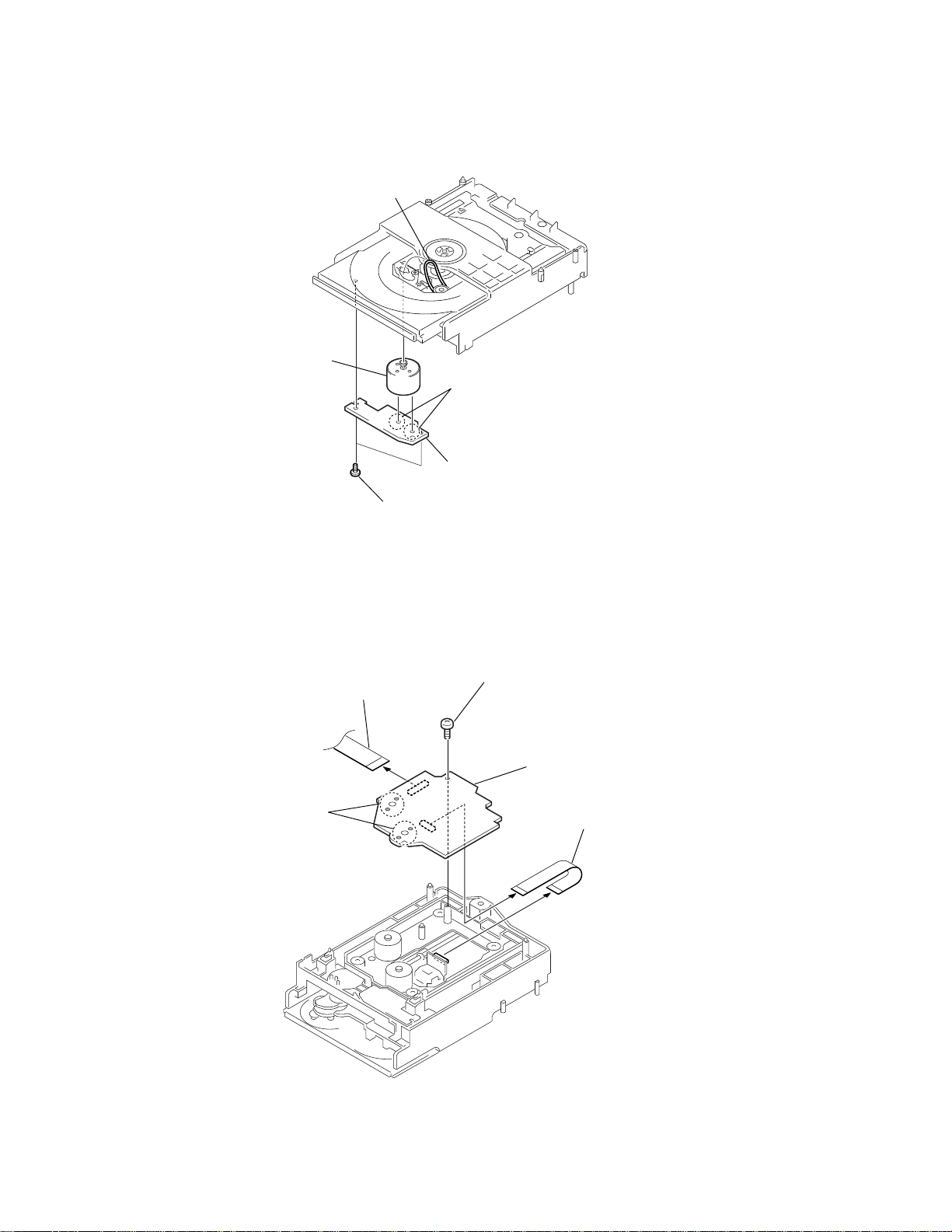
3-6. LOADING Board
4
motor
(M901)
1
(LD) assy
Remove the belt.
3
Remove soldering from the two points.
5
LOADING board
3-7. CD Board
4
wire (flat type) 21p (CN101)
2
Remove soldering
from the four points.
2
two
screws (+BTP 2.6
×
1
screw(+P 2.6
6)
5
CD board
×
5)
3
wire (flat type) 16
10
Page 11
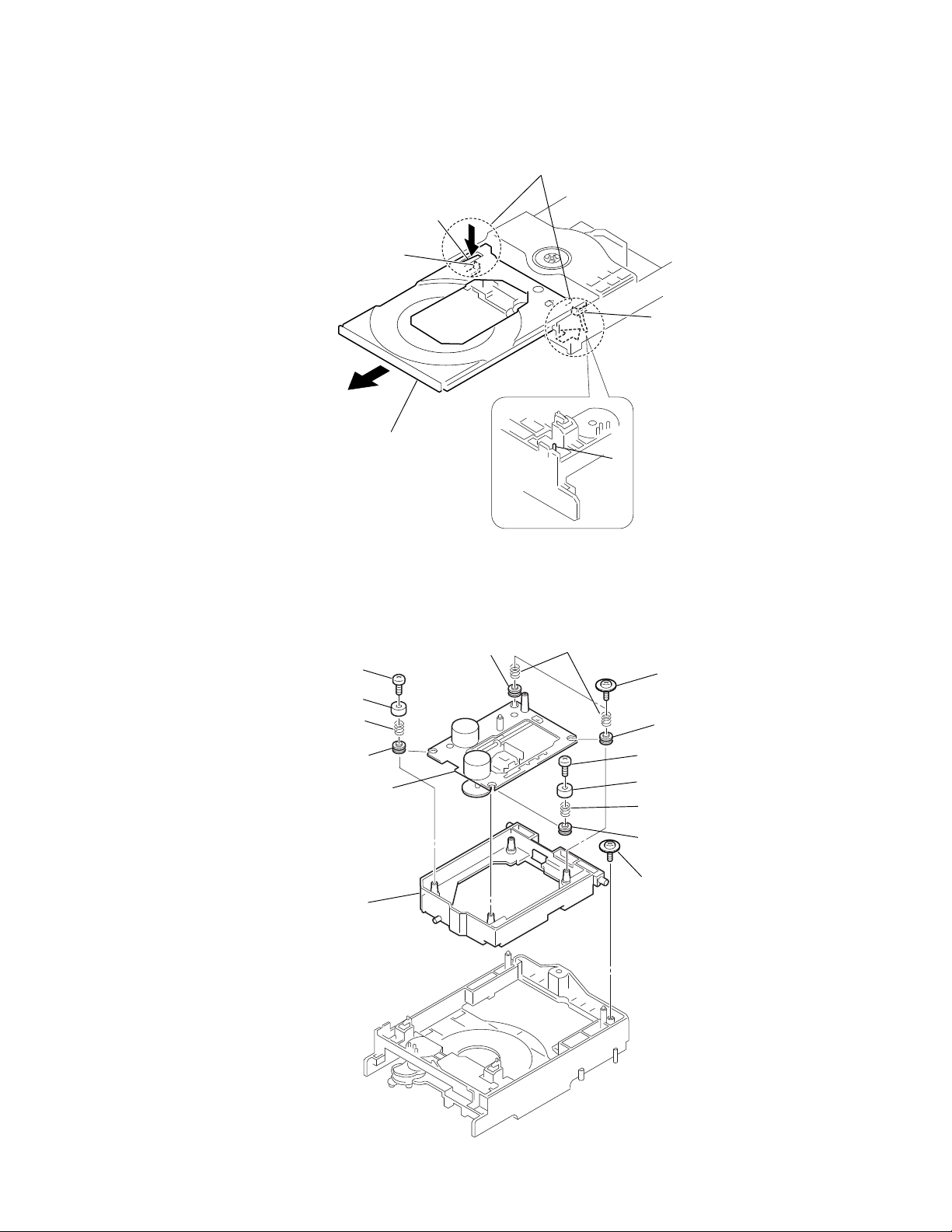
3-8. T ray (CDM55D)
s
1
While pressing the two protrusions A and B to unlock the two claws as shown,
pull the tray in the direction of the arrow
A
claw
C
2
tray
C
. (Be careful of the claws.)
B
claw
CX-LFA500
Ver 1.2 2003.11
3-9. Optical Pick-up (KSM-213D), Holder (C213)
3
5
screw (+PTTP M2.6)
6
stopper (BU)
7
compression spring
(T213)
8
insulator
qd
optical pick-up
(KSM-213D)
qg
holder
(C213)
insulator
2
two compression spring
1
(+PTPWH M2.6)
4
9
screw (+PTTP M2.6)
q;
stopper (BU)
qa
compression spring
(T213)
qs
insulator
qf
floating
(+PTPWH M2.6)
(T213)
two floating
insulator
screws
screw
11
Page 12

CX-LFA500
MEMO
12
Page 13

SECTION 4
MECHANICAL ADJUSTMENTS
Precaution
1. Clean the following parts with a denatured alcohol-moistened
swab:
record/playback heads pinch rollers
erase head rubber belts
capstan idlers
2. Demagnetize the record/playback head with a head demag-
netizer.
3. Do not use a magnetized screwdriver for the adjustments.
4. After the adjustments, apply suitable locking compound to the
parts adjusted.
5. The adjustments should be performed with the rated power
supply voltage unless otherwise noted.
Torque Measurement
Mode
FWD
FWD
back tension
REV
REV
back tension
FF/REW
FWD tension
REV tension
Torque meter Meter reading
2.94 – 7.84 mN • m
CQ-102C
CQ-102C
CQ-102RC
CQ-102RC
CQ-201B
CQ-403A
CQ-403R
(30 to 79 g • cm)
(0.42 – 1.11 oz • inch)
0.15 – 0.59 mN • m
(2 to 6 g • cm)
(0.03 – 0.08 oz • inch)
0.15 – 0.59 mN • m
(2 to 6 g • cm)
(0.03 – 0.08 oz • inch)
0.15 – 0.59 mN • m
(2 to 6 g • cm)
(0.03 – 0.08 oz • inch)
6.86 – 17.64 mN • m
(70 to 179 g • cm)
(0.98 – 2.49 oz • inch)
9.8 mN • m or more
(100 g • cm or more)
(1.4 oz • inch or more)
9.8 mN • m or more
(100 g • cm or more)
(1.4 oz • inch or more)
CX-LFA500
13
Page 14
CX-LFA500
SECTION 5
ELECTRICAL ADJUSTMENTS
DECK SECTION 0 dB=0.775V
1. Demagnetize the record/playback head with a head demagnetizer.
2. Do not use a magnetized screwdriver for the adjustments.
3. After the adjustments, apply suitable locking compound to the
parts adjusted.
4. The adjustments should be performed with the rated power
supply voltage unless otherwise noted.
5. The adjustments should be performed in the order given in this
service manual. (As a general rule, playback circuit adjustment
should be completed before performing recording circuit
adjustment.)
6. The adjustments should be performed for both L-CH and RCH.
7. Switches and controls should be set as follows unless otherwise
specified.
Signal Used forTape
P-4-A100
WS-48B
[Record/Playback Head Azimuth Adjustment]
Procedure:
1. Mode : Playback
test tape
P-4-A100
(10kHz, –10dB)
2. Turn the adjustment screw and check output peaks. If the peaks
do not match for L-CH and R-CH, turn the adjustment screw
so that outputs match within 1 dB of peak.
10 kHz, –10 dB
3 kHz, 0 dB
MAIN board
J203
speaker terminal
set
Azimuth Adjustment
Tape Speed Adjustment
level meter
+
–
3. Mode: Playback
test tape
P-4-A100
(10kHz, –10dB)
in phase 45
MAIN board
J203
speaker terminal
L
set
R
Waveform of oscilloscope
°
90
°
good
135
oscilloscope
°
wrong
180
°
4. After the adjustments, apply suitable locking compound to the
parts adjusted.
Adjustment Location: Record/Playback/Erase Head
[Tape Speed Check]
Procedure:
1. Turn the power on.
2. Insert the WS-48B into deck.
3. Press the Y button of deck.
4. Check the reading of frequency counter becomes 3000 ± 90 Hz.
Sample Value of Wow and flutter
W.RMS (JIS) less than 0.3%
(test tape: WS-48B)
L-CH
peak
screw
position
14
R-CH
peak
output
level
within
1 dB
L-CH
peak
R-CH
peak
within 1dB
screw
position
Page 15

CX-LFA500
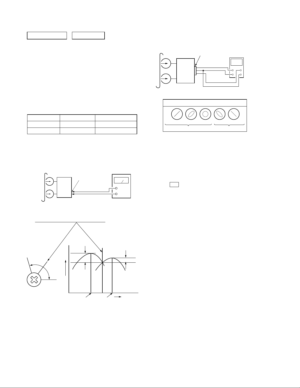
CD SECTION
Note:
1. CD Block is basically designed to operate without adjustment. Therefore, check each item in order given.
2. Use YEDS-18 disc (3-702-101-01) unless otherwise indicated.
3. Use an oscilloscope with more than 10MΩ impedance.
4. Clean the object lens by an applicator with neutral detergent when the
signal level is low than specified value with the following checks.
S-curve Check
Connection:
oscilloscope
CD board
TP (FE)
TP (DVC)
Procedure:
1. Connect an oscilloscope to test point TP (FE) and TP (DVC)
on the CD board.
2. Turn the power on.
3. Put the disc (YEDS-18) in and turned power switch on again
and actuate the focus search. (actuate the focus search when
disc table is moving in and out)
4. Check the oscilloscope waveform (S-curve) is symmetrical
between A and B. And confirm peak to peak level within 2 ± 1
Vp-p.
S-curve waveform
+
–
symmetry
A
B
within 2
±
1 Vp-p
RFDC signal waveform
VOLT/DIV: 200 mV
TIME/DIV: 500 ns
±
level: 0.7
0.2 Vp-p
Checking Location: CD board (Conductor side)
RFAC Level Check
Connection:
oscilloscope
CD board
TP (RFAC)
TP (VC)
+
–
Procedure:
1. Connect an oscilloscope to test point TP (RFAC) and TP (VC)
on the CD board.
2. Turn the power on.
3. Put the disc (YEDS-18) in to playback the number five track.
4. Confirm that oscilloscope waveform is clear and check RFAC
signal level is correct or not.
Note: A clear RFAC signal waveform means that the shape “◊” can be
clearly distinguished at the center of the waveform.
RFAC signal waveform
VOLT/DIV: 200 mV
TIME/DIV: 500 ns
Note: • Try to measure several times to make sure than the ratio of A : B
or B : A is more than 10 : 7.
• Take sweep time as long as possible and light up the
brightness to obtain best waveform.
Checking Location: CD board (Conductor side)
RFDC Level Check
Connection:
oscilloscope
CD board
TP (RFDC)
TP (DVC)
+
–
Procedure:
1. Connect an oscilloscope to test point TP (RFDC) and TP (DVC)
on the CD board.
2. Turn the power on.
3. Put the disc (YEDS-18) in to playback the number five track.
4. Confirm that oscilloscope waveform is clear and check RFDC
signal level is correct or not.
Note: A clear RFDC signal waveform means that the shape “◊” can be
clearly distinguished at the center of the waveform.
level: 0.9
Checking Location: CD board (Conductor side)
±
0.4 Vp-p
15
Page 16

CX-LFA500
E-F Balance Check
Connection:
oscilloscope
CD board
TP (TE)
TP (DVC)
+
–
Procedure:
1. Connect an oscilloscpe to test point TP (TE) and TP (DVC) on
the CD board.
2. AC is put in pushing CD
u button.
3. FL tube carries out all lights and goes into CD test mode.
4. Put the disc (YEDS-18) in to playback the number five track.
5. Press the CD
u button. (The tracking servo and the sledding
servo are turned OFF)
6. Check the level B of the oscilliscope's waveform and the A
(DC voltage) of the center of the Traverse waveform.
Confirm the following :
A/B x 100 = less than ± 22%
Traverse Wa v ef orm
0V
Center of
the waveform
B
A (DC
voltage)
Checking Location:
– CD BOARD (Conductor Side) –
TP (VC)
IC103
TP
(RFAC)
TP (FE)
TP (TE)
TP
(DVC)
IC101
TP
(RFDC)
level: 1.15 ± 0.5 Vp-p
7. Press the CD u button. (The tracking servo and sledding
servo are turned ON)
Confirm the C (DC voltage) is almost equal to the A (DC
voltage) is step 4.
8. To exit from this mode, turn the power off.
Notes: • Always move the optical pick-up to most inside track when
0V
exiting from this mode. Otherwise, a disc will not be unloaded.
• Do not run the sled motor excessively, otherwise the gear can
be chipped.
Traverse Wa v ef orm
Tracking servo
Sled servo
OFF
Tracking servo
Sled servo
ON
C (DC
voltage)
Checking Location: CD board (Conductor side)
16
Page 17

CX-LFA500
1.1Vp-p
1
IC103 qg (RFAC)
(CD Play Mode)
2
IC101 el (FE)
(CD Play Mode)
200mV/DIV,
1
μ
s
/DIV
50mV/DIV,
200
μ
s
/DIV
100mV/DIV,
200
μ
s
/DIV
1V/DIV,
20ns
/DIV
200mVp-p
250mVp-p
3
IC101 ra (TE)
(CD Play Mode)
4
IC101 yj (XTAO)
5.4Vp-p
59ns
11.8Vp-p
s
μ
collector (Rec mode)
Q301
11.7
7
/DIV
s
μ
4
5V/DIV,
– FRONT Board – – MAIN Board –
• Waveforms
– CD Board –
IC601 qd (O-XT2)
5
5.5Vp-p
/DIV
s
μ
s
μ
20
30.5
1V/DIV,
2.7Vp-p
/DIV
40ns
116ns
1V/DIV,
IC601 qh (XOUT)
6
1717
SECTION 6
DIAGRAMS
• Circuit Boards Location
CD BOARD
LOADING BOARD
POWER BOARD
CONTROL BOARD
MAIN BOARD
PHONE BOARD
THIS NOTE IS COMMON FOR PRINTED WIRING
BOARDS AND SCHEMATIC DIAGRAMS.
(In addition to this, the necessary note is printed
in each block.)
These are omitted.
: internal component.
: Pattern from the side which enables seeing.
f
For printed wiring boards.
For schematic diagrams.
•
Note:
• X : parts extracted from the component side.
• Y : parts extracted from the conductor side.
•
• Indication of transistor
W or less unless otherwise
4
/
1
: internal component.
f
specified.
50 WV or less are not indicated except for electrolytics
and tantalums.
• 2 : nonflammable resistor.
• All resistors are in Ω and
•
Note:
• All capacitors are in µF unless otherwise noted. pF: µµF
E
C
Q
B
Replace only with part number specified.
with mark 0 are critical for safety.
Note: The components identified by mark 0 or dotted line
• 1 : fusible resistor.
• C : panel designation.
• A : B+ Line.
• B : B– Line.
These are omitted.
CE
B
Voltage variations may be noted due to normal produc-
tion tolerances.
• Voltages are taken with a VOM (Input impedance 10 MΩ).
• Waveforms are taken with a oscilloscope.
Voltage variations may be noted due to normal produc-
tion tolerances.
• Circled numbers refer to waveforms.
• Signal path.
F : TUNER
J : CD
d : AUX
E : PB (TAPE)
a : REC (TAPE)
Page 18

A
MAIN SECTION
CD
R-CH
L-CH
72
75
LOUT1
LOUT2
X101
16.9344MHz
66
67
XTAI
XTAO
6-1. Block Diagram – CD Section –
CX-LFA500
Ver 1.2 2003.11
IC101 (1/2)
FILTER
BUFFER
AIN1
AIN2
71
76
70
77
AOUT1
AOUT2
&
PWM
INTEGRATOR
FILTER,
DIGITAL
NOISE SHAPER
636261
19
BCK
LRCK
C2PO
PCMD
D/A
INTERFACE
16K
RAM
DIGITAL SIGNAL PROCESSOR,
DIGITAL FILTER, D/A CONVERTER
55
53
54 56
IC103
RF AMP,
FILI
CLTV
PCO
FILO
FOCUS/TRACKING ERROR AMP
CD +5V
DETECTOR
EFM
DIGITAL
ASYMMETRY
RFAC
RFAC
RFAC
IN
EQ
AC
SUM
RF
A
6
A
IN
SERIAL
INTERFACE
INTERNAL BUS
ERROR
CORRECTOR
DEMODULATOR
PLL
CORRECTION
ASYI
ASYO
49
48
51
15
EQ
VCA
3
4
16
17
28
FE
FEI
RFDCO
AMP
RF DC
FOCUS
ERROR AMP
AMP
SUMMING
C
B
D
8
7
9
I-V AMP
D
B
C
LOGIC
TIMING
CLOCK
GENERATOR
: CD
• Signal Path
DOUT
60
OUT
DIGITAL
FOK DETECTOR
TO MIRR/DFCT/
GFS
18
WFCK
EMPH
64 15
SSTP
27
SERVO
SERVO AUTO
SUBCODE
DIGITAL
PWM3
29
RFDCI
F I-V AMP
F
11
F
COUT
9 21
SCLK
INTERFACE
SQCK
SQSO
1 2
SCOR
SEQUENCER
PROCESSOR
CLV
18
TE
TRACKING
E I-V AMP
E
10
E
20
SENS
6
XLAT
CPU INTERFACE
CLOK
DATA
XLON
14 5
XRST
3
MDP
26 7 8
SW
ERROR AMP
BLOCK
KSM-213D
LASER DIODE
OPTICAL PICK-UP
+7V
REG
Q419
CD +5V
+7V
+5V
REG
Q102
+3.3V
S101
(LIMIT)
C-SQCK
C-SQSO
96 88
C-SCOR
C-SENS
94 3
C-DATA
PWM2
2
12
PD
AMP
APC LD
IC102
SPINDLE/SLED MOTOR DRIVE
FOCUS/TRACKING COIL DRIVE,
LD
PD
Q101
LD
1
POWER
CONTROL
AUTOMATIC
C-LD ON
C-XLT
C-CLK
869787
95
PWM2
25
CH4SIN
DRIVE
MOTOR
CH4OUTF
CH4OUTR
15
16
M
(SPINDLE)
IC601 (1/2)
SYSTEM CONTROLLER
C-PWM2
C-PWM1
2
1
PWM3
24
22
23
FOK
DFCT
MIRR
43
39
41
40
IC101 (2/2)
DIGITAL SERVO
RFDC
FE
TE
SE
24
CH3FIN
CH3OUTF
17
PROCESSOR
A/D
CONVERTER
23
CH3RIN
DRIVE
MOTOR
CH3OUTR
18
SRDR
SFDR
282930
FOK
DETECTOR
MIRR/DFCT/
SERVO DSP
FOCUS/TRACKING/SLED
PWM GENERATOR
FOCUS/TRACKING/SLED
TFDR
TRDR
FFDR
FRDR
31
32
33
6
5
CH2FIN
CH2RIN
COIL
DRIVE
CH2OUTR
CH2OUTF
11
12
C-XRST
85
TO SERVO INTERFACE
2
3
20
MUTE
CH1FIN
CH1RIN
COIL
DRIVE
CH1OUTF
CH1OUTR
13
14
1818
M
(SLED)
2-AXIS
DEVICE
(TRACKING)
(FOCUS)
Page 19

IN
AC
CX-LFA500
R CH
Q223,225,229
Q214,216-220
LINE
L801
FILTER
ECO
PT801
TRANS
: TUNER
: CD
: AUX
: PB (TAPE)
: REC (TAPE)
• Signal Path
• R-CH is omitted due to same as L-CH.
DC
DET
Q408,409
J601
HEADPHONES
R CH
Q222
AMP
POWER
Q221,253
PRE
AMP
J203
SPEAKERS
L
L
R
R
R CH
DET
OVER
CURRENT
DC
DET
Q261
MUTE
FL601
DISPLAY
SYSTEM CONTROLLER
MUTE CONT
IC601(2/2)
FLUORESCENT
Q263
9P AMP MUTE
F DATA
10
FIL1 FIL2
.
454750.52
66
SEG1
SEG20
R DATA
R COUNT
99
98
R MUTE
R CE
R TUNED
R CLK
R ST
84
93
80
92
100
KEY
KEY
S614
S615
FUCTION
S608-613
BASE
19
KEY2
FUCTION
S601-607
34
45
18
KEY1
GRID1
GRID11
RDS CLK
RDS SIG23RDS DATA
91
27
S616
TREBLE
ENCODER
20
BASE ENC
VOLUME
ENCODER
ENCODER
21TREBLE ENC
22
VOL ENC
T REC
XT2
XT1
77
12
13
Q201,243
V ECO
Q605
+5V
REG
Q602-604
D608
D610
D602
21
IC603
RESET
μCON +B
ECO
D603
75
LED CONT
X IN
X OUT
T PLAY SW
BIAS81T SW
24
15
79
16
Q601
IC602
REMOTE
RESET
SWITCH
11
25
RESET
SH DET
5
AC
DET
Q412
D417
Q411
HOLD
REG
+VCC
Q406,407
+VCC
POWER
SWITCH
Q610
POWER
CONTROL
31
CONTROL
RECEIVER
8
29
RMC
T MTR CONT6T END SW
25
HOLD
P CONT
T SOL
4
POWER
FIL2
FIL1
D402
D404-407
+7V
REG
REG
+VM
Q416-418
Q402,403,405
Q420
CD POWER
+7V
+VM
DET
2 TIMES
D409,410
CONTROL
REG
-VFL
Q413
+VP
-VFL
82CD FU
PT802
D801-804
Q401 RY801
RELAY
-VP
V ECO
DRIVE
1919
CD DOOR SE
OPEN73CLOSE
28
74
R-CH
16
13
28
CONT
OUT L
OUT R
REC OUT
IC301
PB/REC EQ AMP
TAPE L2CD L
TU L
AUX L
21
19 18
23
+VM
REG
R-CH
J201
L
+10V
R
TUNER UNIT
AUX
6-2. Block Diagram – Main Section –
Q312
X601
X602
8.64MHz
32.768kHz
PB
REC
SWITCH
Q310,311
R-CH
+5V
L-CH
CE
CLK
D IN
R-CH
D OUT
TUNED
R INT
MUTE
R DATA
STEREO
FM SOUT
DECK
L-CH
SWITCH
Q305,306,307
L301
R-CH
R-CH
R-CH
HEAD
REC/PB
+VM
FIN
RIN
OSC
BIAS
Q303
Q301
Q302
Q304
REC BIAS
HEAD
ERASE
MECHA BLOCK
Q609
SW1
SW4
SW3
PLAY
PACK
SW2
F REC
R REC
Q608
Q606
T SOL
DRIVE
DRIVE
MOTOR
R-CH
M
M1
DECK
MOTOR
SW5
PEND
L OUT1
L OUT2
A
CD SECTION
IC604
OUT1
MOTOR DRIVE
4 7
M
TRY
CD OPEN/CLOSE
OUT2
2 9
MOTOR
OPEN
CLOSE
Page 20

D101 F-5
Location
Ref. No. Location
• Semiconductor
IC101 E-4
IC102 C-5
IC103 D-2
Q101 C-2
Q102 G-5
22
CN303
1-680-849-
)
(
• See page 17 for Circuit Boards Location.
TP (VC)
IC102
IC103
TP (RFAC)
TP (DVC)
2020
IC101
345678
12
CX-LFA500
6-3. Printed Wiring Board – CD Section –
Ver 1.2 2003.11
A
B
C
D
E
F
G
Page 21

Ver 1.2 2003.11
CX-LFA500
(KSM-213D)
2121
0uH
• See page 17 for Waveforms. • See page 27, 28 for IC Block Diagrams.
0uH
6-4. Schematic Diagram – CD Section –
23
CN303
Page 22

Ref. No. Location
Ref. No. Location
• Semiconductor Location
11
TO
CN601
BOARD
(Page 24)
CONTROL
C
10
PACK
TUNER
8
Q217 F-4
Q218 F-4
Q219 E-4
Q220 E-4
Q221 E-4
Q222 D-4
D201 B-5
D202 C-5
D203 F-4
D204 D-4
D205 D-4
D206 F-4
R408
224
D416
E
E
E
E
E
Q223 F-3
Q224 D-3
Q225 F-3
Q227 D-3
Q229 E-4
Q243 C-5
Q253 F-4
Q254 D-3
Q261 E-5
Q262 E-5
Q263 E-4
Q301 B-7
Q302 C-7
Q303 B-7
Q304 B-7
Q305 C-7
Q306 C-7
Q307 C-7
Q308 C-8
Q309 D-7
Q310 D-7
Q311 C-7
Q312 B-9
Q401 H-6
Q402 G-4
Q403 G-4
Q405 G-4
Q406 B-5
Q407 B-5
Q408 B-6
Q409 B-6
Q411 B-6
Q412 B-6
Q413 G-8
Q416 G-4
Q417 G-8
Q418 G-9
Q419 F-9
Q420 G-9
D207 F-4
D208 E-4
D209 C-4
D302 E-7
D304 E-7
D305 C-9
D320 C-7
D402 F-6
D404 G-6
D405 G-6
D406 F-6
D407 G-6
D408 G-8
D409 G-8
D410 G-8
D411 G-8
D412 G-8
D414 G-5
D415 G-5
D416 B-9
D417 C-5
D418 B-5
D419 B-9
D420 A-6
D421 F-9
D422 G-9
D424 G-9
D425 G-9
IC301 D-7
Q201 C-5
Q203 C-3
Q204 C-4
Q205 C-4
Q206 D-4
Q207 C-4
Q208 C-5
Q209 D-5
Q210 D-4
Q214 F-5
Q215 C-4
Q216 F-5
REC/PB
ERASE
L-CH
R-CH
TO
CD
CN101
BOARD
(Page 20)
A
7
5
6
234
1
11
D419
E
2
E
E
E
E
E
14
E
IC301
E
2
C475
L401
L402
C474
C319
C317
D304
D302
20
2
L403
C476
R333
TO
CN602
BOARD
(Page 24)
CONTROL
B
1-688-562-
E
TO
CN801
BOARD
POWER
(Page 26)
2222
D
E
1
3
2
R
AUX IN
L
• See page 17 for Circuit Boards Location.
34567 9
12
CX-LFA500
6-5. Printed Wiring Boards – Main Section –
E
E
E
E
E
E
C
B
E
C214
E
C
B
E
E
E
E
E
E
E
E
E
C
B
E
E
E
E
C
B
E
E
E
C
B
E
C
B
+
4
L
2
-
1
L
3
SUBWOOFER
L
+
R
SPEAKERS
-
R
R
MAIN BOARD
R746
PHONE
BOARD
A
B
C
2
3
5
PHONES
1-688-565-
7
4
8
1
D
E
F
G
H
I
Page 23

CX-LFA500
C
D
A
B
TO
J601
PHONES
J203
SPEAKERS
(SPEAKER IMP:6Ω)
L
R
(+)
(+)
(-)
(-)
J204
SUB WOOFER
8.2K
0.45μH
9.8
-23.4
-23.4
-23.3
10
10.1
CN801
BOARD
POWER
(Page 26)
PHONE BOARD
R
J201
AUX
L
PACK
TUNER
CN606
REG
9.8
8.9
9.6
0
0.01
-23.3
0
0
0
22.5
1
1
1
-0.4
0.1
0
0.6
0.6
0
MUTE
Q261,262
25V
25V
-23.3
-1.1
0.1
-1.1
-1.1
-22.6
-1.1
2S
-22.6
1
-22.6
-22.1
-22.3
-22.3
-22.7
-22.1
-22.1
0
-0.9
0.015
50V
50V
50V
50V
0
-23.3
DC DET
-23.3
2S
-23.3
-23.3
-22.7
-23.3
-0.9
0.015
0
0
22.5
1
1
2S
0
0.2
-0.9
0
0
0
0
0
0
0
0
0
0
0
0
0
0
-1.1
1
-0.4
0.1
0
0.6
-22.3
0.6
-22.1
0
0.1
MUTE CONT
0
0
0
0
0
0
0
0
0
0
DC DET
0
-1.1
-23.3
0.1
-1.1
-23.3
-22.7
-1.1
-22.7
-23.3
1
-22..1
-23.3
-22.3
-22.7
-22.7
-22.1
-23.3
-40.6
-32
-4.7
0.1
4.8
50V
50V
0.1
0.047
0.047
22.5
21.8
10.2
0.1
0
0
0.9
V
-32.6
0
50V
2.8
0
330
25V
25V
0.9
0.6
0.2
0.7
DRIVE
RELAY
NOTE:
No mark:FM
RXXX
( ):CD stop
21.2
0.1
0.7
2S
1
0.6
Q402
CONTROL
6.7(0.6)
6.9(0)
7.2(0.8)
CD POWER
6.7(0)
0(4.6)
0(0.6)
22.6
22(21.6)
22(21.5)
25V
0(6.9)
5.6
10.2
9.5
5.1
10.1
2323
0(6.9)
0(5.5)
0(4.9)
0.9
0.3
0.3
0.3
10
• See page 17 for Waveform. • See page 29 for IC Block Diagram.
MAIN BOARD
6-6. Schematic Diagram – Main Section –
10.2
IC301
PB/REC EQ AMP
0
-0.7
0
-0.7
0
-1
-0.9
-1
-1
0
-1
-1
-1
0
TO
CD
TO
CN601
BOARD
CONTOL
(Page 25)
TO
CN602
BOARD
CONTOL
(Page 25)
CN101
BOARD
(Page 21)
0
HEAD
R-CH
(REC/PLAY/ERASE)
10.2
10
-0.7
REC/PB
L-CH
ERASE
10.2
10
10
0.01
RECBIAS
Page 24

3
1
10
Location
D601 B-4
D602 C-8
Ref. No. Location
• Semiconductor
D603 A-10
POWER
D604 C-8
D605 B-3
D606 F-6
D607 C-7
D608 C-8
D609 C-8
D610 B-10
IC601 B-6
IC602 B-9
IC603 C-8
IC604 F-9
Q601 D-7
Q602 B-4
Q603 B-4
Q604 B-4
Q605 B-10
Q606 E-6
Q608 E-6
Q609 F-7
Q610 C-10
STANDBY/ON
REC START
IC602
REC PAUSE
RDS
IC604
1-688-564-
12
(12)
1-674-336-
IC601
BASS
3
4
IC603
7
2
M901
LOADING BOARD
2424
TREBLE
TAPE
DECK
MECHANISM
VOLUME
3456789
• See page 17 for Circuit Boards Location.
12
Ver 1.1 2003.07
CX-LFA500
6-7. Printed Wiring Board – Control Section –
24
2
OPEN/
CLOSE
*
CN602
11P: AEP,UK
12P: EXCEPT AEP,UK
*
(REC MUTING)
CONTROL BOARD
A
TUNER/BAND
C
TO
MAIN
CN302
BOARD
(Page 22)
B
C
D
E
B
TO
MAIN
CN305
BOARD
(Page 22)
F
G
H
Page 25

TO
B
MAIN
CN305
BOARD
(Page 23)
Ver 1.1 2003.07
CX-LFA500
RECEIVER
IC602
REMOTE CONTROL
FLUORESCENT INDICATOR TUBE
VOLUME
STOP
CLOSE
OPEN/
ECO
SLR-342VCT31
5.1
5.1
TREBLE
BASS
AUX
(REC MUTING)
TAPE
TUNER/BAND
CD
REC PAUSE
REC START
SYNCHRO REC
RDS
ECO
STANDBY/ON
POWER
11P: AEP,UK
12P: EXCEPT AEP,UK
NOTE:
No mark:FM
( ):CD stop
S1
(LEAF)
LOADING
BOARD
4.6
M901
(LODING)
010.2
0
10.23.8
+
-
RXXX
3.8
IC604
2525
6
22K
22K
22K
0.01
0.5
5.8
8.7
9.4
• See page 17 for Waveforms. • See page 29 for IC Block Diagrams.
2.4
4.7K
8.1
1.9
2.4
1.6k
u CON
IC601
C-51E3
5
5.0
0
RESET
5.5
RESET
IC603
5.5
25V
Q606
MOTOR
DRIVE
0.5
10.2
TSOL
DRIVE
0
5.1
5.0
POWER
CONTROL
POWER
SWITCH
0
5.1
10.2
0
GR
SWITCH
1.9
0
CONTROL BOARD
6-8. Schematic Diagram – Control Section –
TAPE
MECHANISM
1 0(2.4) 41 -28.6 81 0.3
2 0(2.2) 42 -28.6 82 0(5.0)
3 0 43 -28.7 83 -
4 0.4 44 -28.7 84 0.2
5 5.1 45 -27.9 85 0(5.0)
6 10.1 46 5.0 86 0(5.0)
7 0 47 -21.6 87 0(5.0)
8 5.0 48 -28.0 88 0(5.0)
9 1.2 49 -31.5 89 0
10 0 50 -28.1 90 5.0
11 5.0 51 0 91 2.6
12 2.1 52 -14.9 92 5.0
13 2.5 53 -21.4 93 0
14 0 54 -21.4 94 0(3.2)
15 2.6 55 -21.4 95 0(2.4)
16 2.6 56 -11.4 96 0(3.2)
17 5.0 57 -14.7 97 0(5.0)
18 5.1 58 -21.4 98 0
19 5.1 59 -31.5 99 0
20 5.1 60 -28.0 100 0(0.2)
21 0 61 -15.1
22 5.1 62 -31.5
23 0.8 63 -31.5
24 1.9 64 -28.2
25 2.8 65 -31.5
26 5.5 66 -31.5
27 2.5 67 -
28 0 68 -
29 5.1 69 0
30 - 70 0
31 - 71 0
32 - 72 5.0
33 - 73 0
34 -28.6 74 0
35 -28.6 75 0
36 -28.7 76 -
37 -28.8 77 0
38 -29.2 78 0
39 -28.7 79 4.7
TO
C
MAIN
CN302
BOARD
(Page 23)
NO. VOLT. NO. VOLT. NO. VOLT.
IC601
VOLTAGE CHART
40 -28.7 80 0(5.0)
DECK
Page 26

D
POWER BOARD
AC IN
ECO
*
Not replaceable : Built in transformer
*
TO
MAIN
PN401
BOARD
(Page 23)
5
2
3
*
POWER TRANSFORMER
17
151412
13
Not replaceable : Built in transformer
*
• See page 17 for Circuit Boards Location.
345678
16
2626
1-688-566-
AC IN
4
CX-LFA500
6-9. Printed Wiring Board – Power Section – 6-10. Schematic Diagram – Power Section –
POWER BOARD
12
A
B
7
3
5
1
2
6
8
D
TO
MAIN
PN401
BOARD
(Page 22)
C
D
E
F
G
Page 27

• IC Block Diagrams
– CD Board –
IC101 CXD3017Q
CX-LFA500
LRCK
PCMD
BCK
EMPH
XVDD
XTAI
XTAO
XVSS
AVDD1
AOUT1
AIN1
LOUT1
AVSS1
AVSS2
LOUT2
AIN2
AOUT2
AVDD2
RMUT
LMUT
VDD
AVDD3
PWM
59
58
INTERNAL BUS
VSS
57
ERROR
CORRECTOR
16K
RAM
SUBCODE
PROCESSOR
DOUT
60
DIGITAL
OUT
61
62
63
64
65
66
67
68
69
70
71
72
73
74
75
76
77
78
79
80
D/A
INTERFACE
TIMING
LOGIC
OVER SAMPLING
PWM
3rd ORDER
NOISE SHAPER
DIGITAL FILTER
SERIAL IN
INTERFACE
FILO
FILI
PCO
54
56
55
DIGITAL
PLL
EFM
DEMODULATOR
SERVO
INTERFACE
SERVO AUTO
SEQUENCER
AVSS3
CLTV
52
53
ASYI
BIAS
RFAC
51
49
50
ASYMMETRY
CORRECTOR
48
ASYO
AVDD0
47
46
ADIO
IGEN
AVSS0
45
44
SERVO DSP
FOCUS
SERVO
TRACKING
SERVO
SERVO
ANALOG SWITCH
SLED
CE
TE
RFDC
43
41
42
OPERATIONAL
AMPLIFIER
A/D
CONVERTER
CLOCK
GENERATOR
PWM GENERATOR
FOCUS PWM
GENERATOR
TRACKING
PWM GENERATOR
SLED PWM
GENERATOR
DIGITAL
CLV
MIRR, DFCT,
FOK
DETECTOR
SE
40
FE
39
VC
38
XTSL
37
TES1
36
TEST
35
VSS
34
33
FRDR
32
FFDR
TRDR
31
TFDR
30
SRDR
29
28
SFDR
SSTP
27
MDP
26
25
LOCK
FOK
24
DFCT
23
22
MIRR
3
1
4
2
XRST
SQCK
SQSO
SYSM
IC102 BA5974FP-E2
PRFVCC
CH4BIN
INTERFACE
CH4SIN'
RF
CPU
INTERFACE
9
7
5
6
XLAT
CLOK
DATA
CH4SIN
CH3FIN
CH3RIN
R
F
INTERFACE
F
R
INTERFACE
R
F
F
R
RF
10
8
SENS
CAPAIN3
13
14
11 12
VDD
SCLK
ATSK
SPOA
SPOB
MUTE
1516171819
XUGF
XLON
WFCK
GND
20
GFS
C2PO
XPCK
SCOR
MUTE
POWVCC
CH3OUTR
202122232425262728 19 18 17 16 15
CH3OUTF
THERMAL
SHUTDOWN
LEVEL SHIFT
TR
CH4OU
COUT
21
CH4OUTF
1 2 3 4 5 6 7 8 9 10 11 12 13 14
GND
CH1FIN
VREFOUT
CH1RIN
CH2FIN
CAPAIN1
CH2RIN
CAPAIN2
VREFIN
POWVCC
CH2OUTF
CH2OUTR
CH1OUTR
CH1OUTF
27
Page 28

CX-LFA500
IC103 CXA2581N-T4
DVC
VC
–
+
VOFST
RW/ROM
30
DC OFST
29
A
–
+
B
C
DVC
D
RW/ROM
DVC
VCC
–
+
RFDCI
28
RFDCO
VC
27
VC
EQ IN
AC SUM
GND
SW
DVCC
DVC
RFAC
DVC
APC AMP
A
B
C
D
APC-OFF
RW/ROM
VC
A
(Hi-Z)
(H/L)
RFAC
SUMMING
AMP
BCD
GM
GM
EQ ON/OFF
RW/ROM
B
C
A
D
B
D
A
C
VOFST
–
+
RW/ROM
RW/ROM
–
+
RW/ROM
RW/ROM
VOFST
–
+
RW/ROM
RFAC
VCA
–
+
DVC
VC
VC
–
+
DVC
VC
1
LD
2
PD
3
4
5
6
A
7
B
8
C
9
D
10
E
11
F
12
13
14
15
EQ
VCC
26
RFC
25
VFC
24
BST
23
RFG
22
VCC
CEI
21
20
CE
19
TE BAL
18
TE
17
FEI
16
FE
28
Page 29

– MAIN Board –
IC301 BD3881FV
CX-LFA500
REC-O_L
TAPE-L
TAPE-R
REC-O_R
TUNER-R
TUNER-L
CD-R
CD-L
AUX-R
AUX-L
OUT-L
TON_H-L
TON_L-L
OUT-R
TON_L-R
VSS
TON_H-R
– CONTROL Board –
IC604 BA6956AN
IC603 PST3445UL
TSD
CONTROL LOGIC
1 2 3 4 5 6 7 8 9
VCC
FIN
GND
VREF
RNF
OUT2
VM
OUT1
RIN
29
Page 30

CX-LFA500
6-11. IC Pin Function Description
IC601 LC876764C-51E3 System Control (CONTROL Board)
Pin No.
1
2
3
4
5
6
7
8
9
10
11
12
13
14
15
16
17
18
19
20
21
22
23
24
25
26
27
28
29
30 to 33
34 to 44
45
46
47 to 50
51
52 to 66
67, 68
69 to 71
72
73
74
75
76
77
78
79
80
81
82
83
Pin Name
C-PWM1
C-PWM2
C-SCOR
T-SOL
T-END
T-MTR.CONT
O-SHIFT
P-CON
PAMP-MUTE
F-DATA
I-RESET
I-XT1
O-XT2
GND.
XIN
XOUT
VDD1
I-KEY1
I-KEY2
BASS ENC INPUT
TRBLE ENC INPUT
VOL-ENC
RDS-SIG
T-SW
HOLD
I-SH DET
RDS-CLK
CD-DOOR-SW
RMC-IN
NC
O-GRID1 to 11
O-SEG1
VDD3
O-SEG2 to 5
GND.
O-SEG6 to 20
NC
I-INI-1 to 3
VDD4
O-CLOSE
O-OPEN
LED-CONT
O-DSG
T-REC
I-INI.BASS+2
T-PLAY.SW
R-MUTE
O-BIAS
CD-FU
TUNER
I/O
O
PWM1 signal output to the CD unit
O
PWM2 signal output to the CD unit
I
SCOR (SUBQ request) signal output to the CD unit
O
Solenoid control signal output to the tape deck
I
Tape deck reel switch signal input
O
Motor control signal output to the tape deck
O
Clock shift control signal output
O
Power relay control signal output
O
Muting control signal output to the power amplifier
O
Control signal output to the sound processor
I
Reset signal input from the reset IC (IC603)
I
Resonator terminal (32.768kHz)
O
Resonator terminal (32.768kHz)
—
Ground terminal
I
Resonator terminal (8.64MHz)
O
Resonator terminal (8.64MHz)
—
Power supply terminal
I
Key AD input 1
I
Key AD input 2
I
Encoder signal input from the bass encoder
I
Encoder signal input from the treble encoder
I
Encoder signal input from the volume encoder
I
RDS signal level input from the tuner
I
Tape switch status signal input from the tape deck (SW2 to 4)
I
AC detection signal input
I
DC detection and short circuit detection signal input from the power amplifier
I
RDS clock input from the tuner
I
CD door open/close switch signal input
I
Remote sensor signal input
—
Not used (open)
O
Grid signal output to the fluorescent indicator tube
O
Segment signal output to the fluorescent indicator tube
—
Power supply terminal
O
Segment signal output to the fluorescent indicator tube
—
Ground terminal
O
Segment signal output to the fluorescent indicator tube
—
Not used (open)
I
Initial selection signal input
—
Power supply terminal
O
CD tray close control signal output
O
CD tray open control signal output
O
Standby LED control signal output
O
Not used (open)
O
REC/PLAY control signal output to the REC/PLAY switch circuit
—
Not used (fixed at “L”)
I
Play switch signal input from the tape deck
O
Muting signal output to the tuner
O
Bias control signal output to the bias oscillation circuit
O
CD power supply control signal output
O
Not used (open)
Description
30
Page 31

CX-LFA500
Pin No.
84
85
86
87
88
89
90
91
92
93
94
95
96
97
98
99
100
Pin Name
R-CE
C-XRST
C-XLT
C-DATA
C-SQCK
VSS2
VDD2
RDS-DATA
R-ST
R-TUNED
C-SENS
C-LDON
C-SQSO
C-CLK
R-DATA
R-COUNT
R-CLK
I/O
O
Tuner chip enable signal output to the tuner
O
Reset signal output to the CD unit
O
Latch signal output to the CD unit
O
Data output to the CD unit
O
SUBQ clock output to the CD unit
—
Ground terminal
—
Power supply terminal
I
RDS data input from the tuner
I
Stereo/mono detection signal input from the tuner
I
Tuner tuned status signal input
I
SENS signal input from the CD unit
O
LD ON signal output to the CD unit
I
SUB-Q data input from the CD unit
O
Clock output to the CD unit
O
Data output to the tuner
I
IF count signal input from the tuner
O
Clock signal output to the tuner
Description
31
Page 32

CX-LFA500
Ver 1.1 2003.07
SECTION 7
EXPLODED VIEWS
NOTE:
• -XX, -X mean standardized parts, so they may
have some differences from the original one.
• Items marked “*” are not stocked since they
are seldom required for routine service. Some
delay should be anticipated when ordering these
items.
7-1. Overall Section
2
a
#1
b
• The mechanical parts with no reference number
in the exploded views are not supplied.
• Abbreviation
AUS : Australian model
E51 : Chilean and Peruvian models
KR : Korean model
#3
3
#2
#1
SP : Singapore model
TW : Taiwan model
The components identified by mark 0 or
dotted line with mark 0 are critical for safety .
Replace only with part number specified.
a
#3
#3
#3
4
c
1
front panel assy
c
b
#1
Ref. No. Part No. Description Remark Ref. No. Part No. Description Remark
1 A-4737-500-A CD DOOR ASSY
2 4-247-756-01 CABINET, TOP
3 1-693-619-11 TUNER (FM/AM)(AEP, UK)
3 1-683-620-11 TUNER (FM/AM)(EXCEPT AEP, UK)
04 1-555-795-00 CORD, POWER (EXCEPT TW,KR)
0 4 1-769-079-12 CORD, POWER (KR)
0 4 1-783-531-32 CORD, POWER (TW)
#1 7-685-248-14 SCREW +KTP 3X12 TYPE2 NON-SLIT
#2 7-685-647-79 SCREW +BVTP 3X10 TYPE2 N-S
#3 7-685-647-14 SCREW +BVTP 3X10 TYPE2 N-S
CD block assy
chassis assy
not
supplied
#2
32
Page 33

7-2. Front Section
56
68
59
60
#2
CX-LFA500
Ver 1.3 2004.09
not
supplied
55
52
54
57
not
supplied
53
58
not
not
supplied
#5
supplied
62
61
not
supplied
63
69
64
#2
a
67
65
a
66
51
Ref. No. Part No. Description Remark Ref. No. Part No. Description Remark
51 A-4737-496-A HOLDER CASSETTE ASSY (X)
52 4-238-631-01 TAPE SPRING
53 4-247-757-01 SPR-T,CASS
54 4-245-233-01 KNOB VOL
55 4-245-223-01 KNOB,B/T
56 4-245-226-01 PANEL,L
57 4-245-221-01 BUTTON,REC
58 4-245-217-01 CABINET, FRONT
59 4-245-220-01 BUTTON,POWER
60 A-4732-953-A CONTROL BOARD, COMPLETE (AEP, UK)
60 A-4732-963-A CONTROL BOARD, COMPLETE (E51)
60 A-4734-835-A CONTROL BOARD, COMPLETE (AUS,SP,TW,KR)
61 4-245-219-01 BUTTON,FUNCTION
62 4-245-222-01 BUTTON,CD
63 4-231-841-01 SPRING (HEART CAM-B)
64 4-242-318-01 OIL-DMPR, 70
65 1-796-351-51 MECHANISM, SINGLE CASSETTE
66 4-245-225-01 PANEL,R
67 4-247-752-01 RUBBER, FOOT
68 4-245-227-01 WINDOW, DISPLAY (EXCEPT AEP, UK)
68 4-245-227-11 WINDOW, DISPLAY (AEP, UK)
69 4-231-825-01 CAM (B), HEART
#2 7-685-647-79 SCREW +BVTP 3X10 TYPE2 N-S
#5 3-229-336-01 SCREW +BVWH TAPPING
33
Page 34

CX-LFA500
2
Ver. 1.4
7-3. Chassis Section
not supplied
103
PT801
not supplied
not supplied
#2
#4
#2
101
not supplied
not supplied
#2
108
#2
104
#
#2
not supplied
Ref. No. Part No. Description Remark Ref. No. Part No. Description Remark
101 4-247-752-01 RUBBER, FOOT
103 1-688-566-11 POWER BOARD
104 A-4732-956-A MAIN BOARD, COMPLETE
108 1-688-563-11 HOLD BOARD
0 PT801 1-439-658-11 TRANSFORMER, POWER (AEP, UK,KR)
0 PT801 1-439-660-11 TRANSFORMER, POWER (EXCEPT AEP, UK,KR)
#2 7-685-647-79 SCREW +BVTP 3X10 TYPE2 N-S
#4 7-682-561-09 SCREW +B 4X8
The components identified by mark 0 or dotted
line with mark 0 are critical for safety.
Replace only with part number specified.
34
Page 35

7-4. CD Mechanism Deck Section
CX-LFA500
Ver 1.2 2003.11
not supplied
155
153
156
157
154
158
152
159
161
160
151
#6
162
M901
169
168
not supplied
169
164
not supplied
165
166
167
optical pick-up section
(KSM-213D)
169
170
170
169
171
170
167
172
171
173
163
#7
Ref. No. Part No. Description Remark Ref. No. Part No. Description Remark
151 1-674-336-12 LOADING BOARD
152 4-925-315-31 DAMPER
153 4-224-894-22 TRAY (CDM55D)
154 4-220-233-01 CAM (CDM55)
155 4-221-815-11 ROLLER
156 4-220-237-01 GEAR (A)
157 4-220-234-01 PULLEY (LDG)
158 4-221-816-01 BELT (CDM55)
159 4-227-598-01 SPACER (55)
160 4-220-238-01 GEAR (B)
164 A-473-508-2A MAGNET
165 4-231-777-02 SHEET (KH2)
166 4-244-962-01 HOLDER (C213)
167 4-985-672-01 SCREW (+PTPWH M2.6), FLOATING
168 4-229-358-01 SHAFT (BU21)
169 4-227-549-11 INSULATOR
170 4-244-959-01 SPRING (T213), COMPRESSION
171 4-231-151-01 STOPPER (BU)
172 4-218-253-31 SCREW (M2.6), +BTTP
173 1-757-055-11 WIRE, PARALLEL (FFC) (16 CORE)
161 4-220-229-02 LEVER (SW)
162 4-220-239-01 SPRING, TORSION
163 A-4728-536-A CD BOARD, COMPLETE
M901 A-4735-337-A MOTOR (LD) ASSY (TRAY)
#6 7-685-533-19 SCREW +BTP 2.6X6 TYPE2 N-S
#7 7-621-255-32 SCREW +P 2X5
35
Page 36

CX-LFA500
Ver 1.2 2003.11
7-5. OPTICAL PICK-UP SECTION (KSM-213D)
601
Ref. No. Part No. Description Remark
0601 A-4735-357-A BASE ASSY, OP (KSM-213D)
The components identified by mark 0 or dotted
line with mark 0 are critical for safety.
Replace only with part number specified.
36
Page 37

SECTION 8
ELECTRICAL PARTS LIST
CX-LFA500
Ver 1.1 2003.07
CD
NOTE:
• Due to standardization, replacements in the parts
list may be different from the parts specified in
the diagrams or the components used on the set.
• -XX, -X mean standardized parts, so they may
have some difference from the original one.
• Items marked “*” are not stocked since they are
seldom required for routine service. Some delay
should be anticipated when ordering these items.
• CAPACITORS:
uF: μF
• COILS
uH: μH
Ref. No. Part No. Description Remarks Ref. No. Part No. Description Remarks
A-4728-536-A CD BOARD, COMPLETE
C101 1-162-967-11 CERAMIC CHIP 0.0033uF 10% 50V
C102 1-107-826-11 CERAMIC CHIP 0.1uF 10.00% 16V
C103 1-162-962-11 CERAMIC CHIP 470PF 10% 50V
C104 1-162-962-11 CERAMIC CHIP 470PF 10% 50V
C108 1-107-826-11 CERAMIC CHIP 0.1uF 10.00% 16V
C109 1-162-965-11 CERAMIC CHIP 0.0015uF 10% 50V
C110 1-162-967-11 CERAMIC CHIP 0.0033uF 10% 50V
C111 1-162-927-11 CERAMIC CHIP 100PF 5% 50V
C112 1-115-156-11 CERAMIC CHIP 1uF 10V
C114 1-164-360-11 CE
******************
< CAPACITOR >
RAMIC CHIP 0.1uF 16V
• RESISTORS
All resistors are in ohms.
METAL: metal-film resistor
METAL OXIDE: Metal Oxide-film resistor
F: nonflammable
• SEMICONDUCTORS
In each case, u: μ, for example:
uA...: μA... , uPA... , μPA... ,
uPB... , μPB... , uPC... , μPC... ,
uPD..., μPD...
When indicating parts by reference number,
please include the board name.
C192 1-126-382-11 ELECT 100uF 20.00% 16V
C193 1-126-382-11 ELECT 100uF 20.00% 16V
C194 1-164-360-11 CERAMIC CHIP 0.1uF 16V
C196 1-164-360-11 CERAMIC CHIP 0.1uF 16V
C197 1-107-826-11 CERAMIC CHIP 0.1uF 10.00% 16V
C198 1-126-933-11 ELECT 100uF 20.00% 16V
CN101 1-770-528-31 CONNECTOR, FFC/FPC 21P
CN102 1-779-466-11 CONNECTOR,FFC(LIF(NON-ZIF))16P
D101 8-719-056-77 DIODE UDZ-TE-17-3.9B
• Abbreviation
AUS : Australian model
E51 : Chilean and Peruvian models
KR : Korean model
SP : Singapore model
TW : Taiwan model
The components identified by mark 0 or
dotted line with mark 0 are critical for safety .
Replace only with part number specified.
< CONNECTOR >
< DIODE >
C116 1-126-382-11 ELECT 100uF 20.00% 16V
C117 1-126-382-11 ELECT 100uF 20.00% 16V
C118 1-162-964-11 CERAMIC CHIP 0.001uF 10% 50V
C121 1-164-360-11 CERAMIC CHIP 0.1uF 16V
C122 1-126-933-11 ELECT 100uF 20.00% 16V
C123 1-162-970-11 CERAMIC CHIP 0.01uF 10% 25V
C124 1-125-891-11 CERAMIC CHIP 0.47uF 10.00% 10V
C125 1-164-360-11 CERAMIC CHIP 0.1uF 16V
C126 1-164-360-11 CERAMIC CHIP 0.1uF 16V
C127 1-126-382-11 ELECT 100uF 20.00% 16V
C130 1-164-360-11 CERAMIC CHIP 0.1uF 16V
C131 1-126-933-11 ELECT 100uF 20.00% 16V
C133 1-162-921-11 CERAMIC C
C140 1-115-156-11 CERAMIC CHIP 1uF 10V
C143 1-164-360-11 CERAMIC CHIP 0.1uF 16V
C145 1-164-360-11 CERAMIC CHIP 0.1uF 16V
C146 1-107-826-11 CERAMIC CHIP 0.1uF 10.00% 16V
C153 1-164-360-11 CERAMIC CHIP 0.1uF 16V
C159 1-162-969-11 CERAMIC CHIP 0.0068uF 10% 25V
C162 1-126-382-11 ELECT 100uF 20.00% 16V
C163 1-126-933-11 ELECT 100uF 20.00% 16V
C165 1-164-360-11 CERAMIC CHIP 0.1uF 16V
C167 1-162-920-11 CERAMIC CHIP 27PF 5% 50V
C168 1-162-919-11 CERAMIC CHIP 22PF 5% 50V
C171 1-115-412-11 CERAMIC CHIP
C172 1-162-927-11 CERAMIC CHIP 100PF 5% 50V
C181 1-115-412-11 CERAMIC CHIP 680PF 5.00% 25V
C182 1-162-927-11 CERAMIC CHIP 100PF 5% 50V
C183 1-162-968-11 CERAMIC CHIP 0.0047uF 10% 50V
C184 1-162-968-11 CERAMIC CHIP 0.0047uF 10% 50V
C185 1-125-891-11 CERAMIC CHIP 0.47uF 10.00% 10V
C190 1-115-156-11 CERAMIC CHIP 1uF 10V
C191 1-126-933-11 ELECT 100uF 20.00% 16V
HIP 33PF 5% 50V
680PF 5.00% 25V
< FERRITE BEAD >
FB101 1-469-144-21 FERRITE0uH
FB103 1-469-144-21 FERRITE0uH
< IC >
IC101 8-752-402-31 IC CXD3017Q
IC102 8-759-549-28 IC BA5974FP-E2
IC103 8-752-089-74 IC CXA2581N-T4
< JUMPER RESISTOR >
JR101 1-216-864-11 METAL CHIP 0
< TRANSISTOR >
Q101 8-729-049-31 TRANSISTOR 2SB710A-RTX
Q102 8-729-920-85 TRANSISTOR 2SD1664-T100-QR
< RESISTOR >
R101 1-216-821-11 ME
R102 1-216-845-11 METAL CHIP 100K 5% 1/10W
R103 1-216-835-11 METAL CHIP 15K 5% 1/10W
R104 1-216-839-11 METAL CHIP 33K 5% 1/10W
R106 1-216-821-11 METAL CHIP 1K 5% 1/10W
R107 1-216-833-11 METAL CHIP 10K 5% 1/10W
R108 1-216-827-11 METAL CHIP 3.3K 5% 1/10W
R109 1-216-857-11 METAL CHIP 1M 5% 1/10W
R111 1-216-846-11 METAL CHIP 120K 5% 1/10W
R114 1-218-745-11 METAL C
R116 1-216-797-11 METAL CHIP 10 5% 1/10W
R117 1-216-821-11 METAL CHIP 1K 5% 1/10W
R118 1-216-809-11 METAL CHIP 100 5% 1/10W
R119 1-216-826-11 METAL CHIP 2.7K 5% 1/10W
R120 1-216-835-11 METAL CHIP 15K 5% 1/10W
TAL CHIP 1K 5% 1/10W
HIP 160K 5% 1/10W
37
Page 38

CX-LFA500
Ver 1.1 2003.07
CD CONTROL
Ref. No. Part No. Description Remarks Ref. No. Part No. Description Remarks
R122 1-216-845-11 METAL CHIP 100K 5% 1/10W
R123 1-216-833-11 METAL CHIP 10K 5% 1/10W
R124 1-216-845-11 METAL CHIP 100K 5% 1/10W
R131 1-216-813-11 METAL CHIP 220 5% 1/10W
R143 1-216-836-11 METAL CHIP 18K 5% 1/10W
R144 1-216-836-11 METAL CHIP 18K 5% 1/10W
R147 1-216-828-11 METAL CHIP 3.9K 5% 1/10W
R148 1-216-797-11 METAL CHIP 10 5% 1/10W
R149 1-216-797-11 METAL CHIP 10 5% 1/10W
R150 1-216-833-11 METAL C
R151 1-216-845-11 METAL CHIP 100K 5% 1/10W
R158 1-216-837-11 METAL CHIP 22K 5% 1/10W
R159 1-216-837-11 METAL CHIP 22K 5% 1/10W
R162 1-216-847-11 METAL CHIP 150K 5% 1/10W
R171 1-216-837-11 METAL CHIP 22K 5% 1/10W
R172 1-216-837-11 METAL CHIP 22K 5% 1/10W
R173 1-216-837-11 METAL CHIP 22K 5% 1/10W
R181 1-216-837-11 METAL CHIP 22K 5% 1/10W
R182 1-216-837-11 METAL CHIP 22
R183 1-216-837-11 METAL CHIP 22K 5% 1/10W
R190 1-216-813-11 METAL CHIP 220 5% 1/10W
R191 1-216-839-11 METAL CHIP 33K 5% 1/10W
R192 1-216-839-11 METAL CHIP 33K 5% 1/10W
R193 1-216-846-11 METAL CHIP 120K 5% 1/10W
R194 1-216-845-11 METAL CHIP 100K 5% 1/10W
R195 1-216-853-11 METAL CHIP 470K 5% 1/10W
R196 1-216-825-11 METAL CHIP 2.2K 5% 1/10W
R197 1-216-821-11 METAL CHIP 1K 5% 1/10W
RN101 1-233-576-11 RES, CHIP NETWORK 100
S101 1-771-853-11 SWITCH, DETECTION (LIMIT)
X101 1-767-226-11 VIBRATOR, CRYSTAL (16.9344 MHz)
************************************************************
A-4732-953-A CONTROL BOARD, COMPLETE (AEP, UK)
A-4732-963-A CONTROL BOARD, COMPLETE (E51)
A-4734-835-A CONTROL BOARD, COMPLETE (AUS,SP,TW,KR)
4-247-818-01 GUIDE (FL)
4-247-819-01 HOLDER, SENSOR
4-247-820-01 FILTER, FL
C601 1-164-218-91 CERAMIC CHIP 180PF 5.00% 50V
C603 1-164-156-11 CERAMIC CHIP 0.1uF 25V
C604 1-162-927-11 CERAMIC CHIP 100PF 5% 50V
C605 1-162-962-11 CERAMIC CHIP 470PF 10% 50V
C606 1-126-963-11 ELECT 4.7uF 20.00% 50V
C607 1-126-963-11 ELECT 4.7uF 20.00% 50V
C608 1-126-916-11 ELECT 1000uF 20.00% 6.3V
C609 1-162-970-11 CERAMIC CHIP 0.01uF 10.00% 25V
C610 1-164-156-11 CERAMIC CHIP 0.1uF 25V
C611 1-104-665-11 ELECT 100uF 20.00% 10V
HIP 10K 5% 1/10W
K 5% 1/10W
NETWORK >
<
< SWITCH >
< VIBRATOR >
************************
< CAPACITOR >
C612 1-104-662-11 ELECT 22uF 20.00% 25V
C613 1-164-156-11 CERAMIC CHIP 0.1uF 25V
C614 1-164-156-11 CERAMIC CHIP 0.1uF 25V
C615 1-164-156-11 CERAMIC CHIP 0.1uF 25V
C616 1-162-918-11 CERAMIC CHIP 18PF 50V
C616 1-162-912-11 CERAMIC CHIP 7PF 50V
C617 1-162-919-91 CERAMIC CHIP 22PF 5.00% 50V
C618 1-162-921-11 CERAMIC CHIP 33PF 5% 50V
C620 1-162-970-11 CERAMIC CHIP 0.01uF 10% 25V
C621 1-162-970-11 CERAMIC CHIP 0.01uF 10% 25V
C622 1-162-970-11 CERAMIC C
C623 1-162-927-91 CERAMIC CHIP 100PF 10% 50V
C624 1-104-660-11 ELECT 47uF 20.00% 16V
C625 1-162-970-91 CERAMIC CHIP 0.01uF 10% 25V
C632 1-162-927-11 CERAMIC CHIP 100PF 5% 50V
C633 1-162-927-11 CERAMIC CHIP 100PF 5% 50V
C634 1-162-927-11 CERAMIC CHIP 100PF 5% 50V
C635 1-162-927-11 CERAMIC CHIP 100PF 5% 50V
C636 1-162-927-11 CERAMIC CHIP 100PF 5% 50V
C637 1-162-927-11 CERAMIC CHIP 100PF 5% 50V
C639 1-162-970-11 CERAMIC CHIP 0.01uF 10% 25V
C640 1-162-970-11 CERAMIC CHIP 0.01uF 10% 25V
C641 1-162-970-11 CER
C642 1-162-970-11 CERAMIC CHIP 0.01uF 10% 25V
C643 1-162-970-11 CERAMIC CHIP 0.01uF 10% 25V
C644 1-162-970-11 CERAMIC CHIP 0.01uF 10% 25V
C646 1-126-964-11 ELECT 10uF 20.00% 50V
C649 1-162-970-11 CERAMIC CHIP 0.01uF 10% 25V
C650 1-162-970-11 CERAMIC CHIP 0.01uF 10% 25V
C651 1-162-964-11 CERAMIC CHIP 0.001uF 10% 50V
C652 1-164-156-11 CERAMIC CHIP 0.1uF 25V
C653 1-126-964-11 ELECT 10uF 20.00% 50V
C654 1-164-156-11 CERAMIC CHIP 0.1uF 25V
C655 1-162-970-11 CERAMIC CHIP 0.01u
C656 1-126-933-11 ELECT 100uF 20.00% 16V
C657 1-164-156-11 CERAMIC CHIP 0.1uF 25V
C658 1-164-156-11 CERAMIC CHIP 0.1uF 25V
C661 1-126-963-11 ELECT 4.7uF 20.00% 50V
C662 1-126-960-11 ELECT 1uF 20.00% 50V
C663 1-162-917-11 CERAMIC CHIP 15PF 5% 50V
C664 1-164-156-11 CERAMIC CHIP 0.1uF 25V
C665 1-162-927-11 CERAMIC CHIP 100PF 5% 50V
C668 1-162-911-11 CERAMIC CHIP 6PF 50V
C669 1-162-927-11 CERAMIC CHIP 100PF 5% 50V
C670 1-162-927-11 CERAMIC CHIP 100PF 5% 50V
< CONNECTOR >
CN601 1-779-562-21 CONNEC
CN602 1-779-280-11 CONNECTOR,FFC(LIF(NON-ZIF))12P
CN602 1-784-733-11 CONNECTOR,FFC 11P (AEP, UK)
* CN603 1-770-516-31 CONNECTOR, FFC/FPC 8P
* CN605 1-564-508-11 PLUG, CONNECTOR 5P
< DIODE >
D601 8-719-010-41 DIODE UZ-5.6BSA-TP
HIP 0.01uF 10% 25V
AMIC CHIP 0.01uF 10% 25V
F 10% 25V
TOR,FFC(LIF(NON-ZIF))25P
(AEP, UK,E51)
(AUS,SP,TW,KR)
(AEP, UK,E51)
(EXCEPT AEP, UK)
38
Page 39

CX-LFA500
Ver 1.1 2003.07
CONTROL
Ref. No. Part No. Description Remarks Ref. No. Part No. Description Remarks
D602 8-719-911-19 DIODE 1SS133T-72
D603 8-719-059-98 DIODE SLR-342VCT31 (ECO)
D604 8-719-911-19 DIODE 1SS133T-72
D605 8-719-911-19 DIODE 1SS133T-72
D606 8-719-911-19 DIODE 1SS133T-72
D607 8-719-911-19 DIODE 1SS133T-72
D608 8-719-989-91 DIODE 1N4148A-T265
D609 8-719-989-91 DIODE 1N4148A-T265
D610 8-719-911-19 DIODE 1SS133T-72
< FERRITE BEAD >
FB601 1-410-396-41 FERRITE 0.45uH (AEP,UK,E51)
FB601 1-412-473-11 INDUCTOR 0uH (AUS,SP,TW,KR)
FB602 1-412-473-11 INDUCTOR 0uH
< FILTER >
L601 1-518-886-11 INDICATOR TUBE, FLUORESCENT
F
< IC >
IC601 6-802-784-01 IC LC876764C-51E3
IC602 6-600-092-01 IC RPM7138-V4
IC603 6-700-250-01 IC PST3445UL
IC604 8-759-598-69 IC BA6956AN
< JUMPER RESISTOR >
R611 1-216-809-11 METAL CHIP 100 5% 1/10W
R612 1-249-429-11 CARBON 10K 5% 1/4W
R613 1-249-417-11 CARBON 1K 5% 1/4WF
R614 1-249-417-11 CARBON 1K 5% 1/4WF
R615 1-249-417-11 CARBON 1K 5% 1/4WF
R616 1-249-417-11 CARBON 1K
R617 1-249-417-11 CARBON 1K 5% 1/4WF
R618 1-249-417-11 CARBON 1K 5% 1/4WF
R619 1-216-845-11 METAL CHIP 100K 5% 1/10W
R620 1-216-829-11 METAL CHIP 4.7K 5% 1/10W
R621 1-216-821-11 METAL CHIP 1K 5% 1/10W
R622 1-216-835-11 METAL CHIP 15K 5% 1/10W
R623 1-216-817-11 METAL CHIP 470 5% 1/10W
R624 1-216-073-91 RES-CHIP 10K 5% 1/10W
R625 1-216-825-11 METAL CHIP 2.2K 5% 1/10W
R626 1-216-833-11 METAL CHIP 10K 5% 1/10W
R627 1-216-825-11 METAL CHIP 2.2K 5% 1/10W
R631 1-216-837-11 METAL CHIP 22K 5% 1/16W
R632 1-216-845-11 METAL CHIP 100K 5% 1/10W
R633 1-216-845-11 METAL CHIP 100K 5% 1/10W
R634 1-216-833-11 METAL CHIP 10K 5% 1/10W
R635 1-216-845-11 METAL CHIP 100K 5% 1/10W
R636 1-216-845-11 METAL CHIP 100K 5% 1/10W
R637 1-216-845-11 METAL CHIP 100K 5% 1/10W
R638 1-216-845-11 METAL CHIP 100K 5% 1/10
5% 1/4WF
W
JR601 1-216-295-91 SHORT CHIP 0
JR602 1-216-864-11 METAL CHIP 0
JR603 1-216-864-11 METAL CHIP 0
< COIL >
L601 1-410-509-21 INDUCTOR 10uH
L602 1-410-509-21 INDUCTOR 10uH
< TRANSISTOR >
Q601 8-729-230-49 TRANSISTOR 2SC2712L-TE85R
Q602 6-550-296-01 TRANSISTOR 2SA1980G
Q603 8-729-230-49 TRANSISTOR 2SC2712L-TE85R
Q604 8-729-230-49 TRANSISTOR 2SC2712L-TE85R
Q605 8-729-029-21 TRANSISTOR DTA114ESA
Q606 6-550-305-01 TRANSISTOR 2SA1296GR
Q608 6-550-297-01 TRANSISTOR
Q609 8-729-027-43 TRANSISTOR DTC114EK
Q610 8-729-027-44 TRANSISTOR DTC114TK
< RESISTOR >
R601 1-216-828-11 METAL CHIP 3.9K 5% 1/16W
R601 1-216-833-11 METAL CHIP 10K 5% 1/16W
R602 1-249-417-11 CARBON 1K 5% 1/4WF
R603 1-216-821-11 METAL CHIP 1K 5% 1/10W
R604 1-216-821-11 METAL CHIP 1K 5% 1/10W
R605 1-216-821-11 METAL CHIP 1K 5% 1/10W
R606 1-247-767-11 CARBON 2.2 5% 1/4W
R607 1-247-807-31 CARBON 100 5% 1/4W
R608 1-247-807-31 CARBON 100 5% 1/4W
R609 1-216-864-11 METAL CHIP 0
R610 1-216-809-11 METAL CHIP 100 5% 1/10W
2SA1981Y
(AUS,SP,TW,KR)
(AEP, UK,E51)
R639 1-216-845-11 METAL CHIP 100K 5% 1/10W
R640 1-216-845-11 METAL CHIP 100K 5% 1/10W
R641 1-216-845-11 METAL CHIP 100K 5% 1/10W
R642 1-216-845-11 METAL CHIP 100K 5% 1/10W
R643 1-216-845-11 METAL CHIP 100K 5% 1/10W
R644 1-216-845-11 METAL CHIP 100K 5% 1/10W
R645 1-216-845-11 METAL CHIP 100K 5% 1/10W
R646 1-216-845-11 METAL CHIP 100K 5% 1/10W
R647 1-216-845-11 METAL CHIP 100K 5% 1/10W
R648 1-216-845-11 METAL CHIP 100K 5% 1/10W
R649 1-216-845-11 METAL CHIP 100K 5% 1/10W
R650 1-216-845-11 METAL CHIP 100K 5% 1/10W
R651 1-216-845-11 METAL CHIP 100K 5% 1/10W
R652 1-216-845-11 METAL CHIP 100K 5% 1/10W
R653 1-216-845-11 METAL CHIP 100K 5% 1/10W
R654 1-216-845-11 METAL CHIP 100K 5% 1/10W
R655 1-216-845-11 METAL CHIP 100K 5% 1/10W
R656 1-216-845-11 METAL CHIP 100K 5% 1/10W
R657 1-216-845-11 M
R658 1-216-845-11 METAL CHIP 100K 5% 1/10W
R659 1-216-835-11 METAL CHIP 15K 5% 1/10W
R660 1-216-845-11 METAL CHIP 100K 5% 1/10W
R661 1-216-845-11 METAL CHIP 100K 5% 1/10W
R662 1-216-841-11 METAL CHIP 47K 5% 1/10W
R663 1-216-841-11 METAL CHIP 47K 5% 1/10W
R664 1-247-887-00 CARBON 220K 5% 1/4W
R665 1-216-841-11 METAL CHIP 47K 5% 1/10W
R666 1-216-821-11 METAL CHIP
R667 1-216-853-11 METAL CHIP 470K 5% 1/10W
R668 1-216-809-11 METAL CHIP 100 5% 1/10W
R669 1-216-829-11 METAL CHIP 4.7K 5% 1/10W
R670 1-216-833-11 METAL CHIP 10K 5% 1/10W
R671 1-216-841-11 METAL CHIP 47K 5% 1/10W
ETAL CHIP 100K 5% 1/10W
1K 5% 1/10W
39
Page 40

CX-LFA500
Ver 1.1 2003.07
CONTROL LOADING MAIN
Ref. No. Part No. Description Remarks Ref. No. Part No. Description Remarks
R672 1-216-841-11 METAL CHIP 47K 5% 1/10W
R674 1-216-833-11 METAL CHIP 10K 5% 1/10W
R675 1-216-837-11 METAL CHIP 22K 5% 1/10W
R676 1-216-837-11 METAL CHIP 22K 5% 1/10W
R677 1-216-839-11 METAL CHIP 33K 5% 1/10W
R678 1-216-837-11 METAL CHIP 22K 5% 1/10W
R679 1-216-841-11 METAL CHIP 47K 5% 1/10W
R680 1-249-417-11 CARBON 1K 5% 1/4WF
R681 1-249-417-11 CARBON 1K 5% 1/4WF
R682 1-216-815-11 ME
R683 1-216-838-11 METAL CHIP 27K 5% 1/10W
R684 1-216-830-11 METAL CHIP 5.6K 5% 1/10W
R685 1-216-845-11 METAL CHIP 100K 5% 1/10W
TAL CHIP 330 5% 1/10W
R735 1-249-417-11 CARBON 1K 5% 1/4
R736 1-216-821-11 METAL CHIP 1K 5% 1/10W
R737 1-216-833-11 METAL CHIP 10K 5% 1/10W
R738 1-216-833-11 METAL CHIP 10K 5% 1/10W
R739 1-216-845-11 METAL CHIP 100K 5% 1/10W
R740 1-216-845-11 METAL CHIP 100K 5% 1/10W
R741 1-216-845-11 METAL CHIP 100K 5% 1/10W
R743 1-216-829-11 METAL CHIP 4.7K 5% 1/10W
R748 1-216-837-11 METAL CHIP 22K 5% 1/16W
R750 1-216-837-11 METAL CHIP 22K 5% 1/16W
R
780 1-216-864-11 METAL CHIP 0
R781 1-247-879-11 CARBON 100K 5% 1/10W
R791 1-216-845-11 METAL CHIP 100K 5% 1/10W
WF
R686 1-260-070-11 CARBON 3.3 5% 1/2W
R687 1-216-830-11 METAL CHIP 5.6K 5% 1/10W
R688 1-216-833-11 METAL CHIP 10K 5% 1/10W
R689 1-216-809-11 METAL CHIP 100 5% 1/10W
R690 1-216-809-11 METAL CHIP 100 5% 1/10W
R691 1-216-809-11 METAL CHIP 100 5% 1/10W
R692 1-216-809-11 METAL CHIP 100 5% 1/10W
R693 1-216-809-11 METAL CHIP 100 5% 1/10W
R694 1-216-809-11 METAL CHIP 100 5% 1/10W
R695 1-216-809-11 METAL CHIP 100 5% 1/10W
R696 1-216-809-11 METAL CHIP 100 5% 1/10W
R697 1-216-809-11 METAL CHIP 100 5% 1/10W
R698 1-216-809-11 METAL CHIP 100 5% 1/10W
R699 1-216-809-11 METAL CHIP 100 5% 1/10W
R701 1-216-833-11 METAL CHIP 10K 5% 1/10W
R702 1-249-417-11 CARBON 1K 5% 1/4WF
R703 1-216-837-11 METAL CHIP 22K 5% 1/10W
R704 1-216-833-11 MET
R705 1-216-833-11 METAL CHIP 10K 5% 1/10W
R706 1-218-179-11 METAL CHIP 10M 5% 1/10W
R707 1-216-833-11 METAL CHIP 10K 5% 1/10W
R708 1-216-837-11 METAL CHIP 22K 5% 1/10W
R709 1-216-833-11 METAL CHIP 10K 5% 1/10W
R711 1-216-845-11 METAL CHIP 100K 5% 1/10W
R712 1-216-833-11 METAL CHIP 10K 5% 1/10W
R713 1-216-837-11 METAL CHIP 22K 5% 1/10W
R714 1-216-833-11 METAL CHIP
R715 1-216-833-11 METAL CHIP 10K 5% 1/10W
R716 1-216-823-11 METAL CHIP 1.5K 5% 1/10W
R717 1-216-824-11 METAL CHIP 1.8K 5% 1/10W
R718 1-216-826-11 METAL CHIP 2.7K 5% 1/10W
R719 1-216-828-11 METAL CHIP 3.9K 5% 1/10W
R720 1-218-867-11 METAL CHIP 6.8K 5% 1/10W
R721 1-216-832-11 METAL CHIP 8.2K 5% 1/10W
R722 1-216-823-11 METAL CHIP 1.5K 5% 1/10W
R723 1-216-824-11 METAL CHIP 1.8K
R724 1-216-826-11 METAL CHIP 2.7K 5% 1/10W
R725 1-249-424-11 CARBON 3.9K 5% 1/4WF
R726 1-218-867-11 METAL CHIP 6.8K 5% 1/10W
R727 1-216-845-11 METAL CHIP 100K 5% 1/10W
R728 1-249-425-11 CARBON 4.7K 5% 1/4WF
R729 1-249-425-11 CARBON 4.7K 5% 1/4WF
R730 1-249-417-11 CARBON 1K 5% 1/4WF
R731 1-216-833-11 METAL CHIP 10K 5% 1/10W
R732 1-216-830-11 METAL CHIP 5.6K 5% 1/10W
AL CHIP 10K 5% 1/10W
10K 5% 1/10W
5% 1/10W
< SWITCH >
S601 1-786-050-21 SWITCH, KEY BOARD (TUNER)
S602 1-786-050-21 SWITCH, KEY BOARD (TAPE (REC MUTING))
S603 1-786-050-21 SWITCH, KEY BOARD (AUX)
S604 1-786-050-21 SWITCH, KEY BOARD (Z OPEN/CLOSE)
S605 1-786-050-21 SWITCH, KEY BOARD (STO
S606 1-786-050-21 SWITCH, KEY BOARD (+ >)
S607 1-786-050-21 SWITCH, KEY BOARD (- .)
S608 1-786-050-21 SWITCH, KEY BOARD (POWER, STANDBY/ON)
S609 1-786-050-21 SWITCH, KEY BOARD (ECO)
S610 1-786-050-21 SWITCH, KEY BOARD (RDS)
S611 1-786-050-21 SWITCH, KEY BOARD (SYNCHRO REC)
S612 1-786-050-21 SWITCH, KEY BOARD (REC START, REC PAUSE)
S613 1-786-050-21 SWIT
S614 1-786-395-11 SW, RTRY RE0123PVB25FINA 1-2 (BASS)
S615 1-786-395-11 SW, RTRY RE0123PVB25FINA 1-2 (TREBLE)
S616 1-477-823-11 ENCODER, ROTARY (VOLUME)
X601 9-300-001-87 VIB,XTAL 32.768kHZ CFS-308 CT
X602 1-795-880-11 VIBRATOR, CERAMIC (8.64MHz)
************************************************************
1-674-336-12 LOADING BOARD
* CN151 1-568-943-11 PIN, CONN
S1 1-786-203-11 SWITCH, LEVER (SLIDE) (OPEN/CLOSE)
************************************************************
A-4732-956-A MAIN BOARD, COMPLETE
C1 1-137-376-11 FILM 0.1uF 5% 50V
C2 1-137-376-11 FILM 0.1uF 5% 50V
C202 1-126-925-11 ELECT 470uF 20% 10V
C205 1-162-970-11 CERAMIC CHIP 0.01uF 10% 25V
C207 1-164-360-91 CERAMIC CHIP 0.1uF 16V
C214 1-104-664-11 ELECT 47uF 20% 25V
C217 1-164-343-91 CERAMIC CHIP 0.056uF 10% 25V
CH, KEY BOARD (CD)
< VIBRATOR >
*************
< CONNECTOR >
ECTOR 5P
< SWITCH >
*********************
< CAPACITOR >
P)
40
Page 41

CX-LFA500
MAIN
Ref. No. Part No. Description Remarks Ref. No. Part No. Description Remarks
C218 1-164-343-91 CERAMIC CHIP 0.056uF 10% 25V
C219 1-164-156-11 CERAMIC CHIP 0.1uF 25V
C220 1-164-156-11 CERAMIC CHIP 0.1uF 25V
C221 1-164-245-11 CERAMIC CHIP 0.015uF 10.00% 25V
C222 1-164-245-11 CERAMIC CHIP 0.015uF 10.00% 25V
C223 1-164-156-11 CERAMIC CHIP 0.1uF 25V
C224 1-164-156-11 CERAMIC CHIP 0.1uF 25V
C225 1-162-970-11 CERAMIC CHIP 0.01uF 10% 25V
C227 1-162-968-11 CERAMIC CHIP 0.0047uF 10% 50V
C233 1-164-245-91 CERAMIC CHIP 0.015uF 10.00% 25V
C234 1-164-245-91 CERAMIC CHIP 0.015uF 10.00% 25V
C235 1-162-970-11 CERAMIC CHIP 0.01uF 10% 25V
C236 1-126-959-11 ELECT 0.47uF 20% 50V
C238 1-162-966-11 CERAMIC CHIP 0.0022uF 10% 50V
C239 1-104-660-11 ELECT 47uF 20% 16V
C243 1-104-665-11 ELECT 100uF 20.00% 10V
C244 1-164-230-11 CERAMIC CHIP 220PF 5.00% 50V
C246 1-104-665-11 ELECT 100uF 20.00% 10V
C247 1-126-959-11 ELECT 0.47uF 20% 50V
C248 1-164-230-11 CERAMIC CHIP 220PF 5.00% 50V
C251 1-164-230-11 CERAMIC CHIP 220PF 5.00% 50V
C252 1-162-927-11 CERAMIC CHIP 100PF 5% 50V
C253 1-164-230-11 CERAMIC CHIP 220PF 5.00% 50V
C257 1-126-947-11 ELECT 47uF 20.00% 25V
C275 1-162-927-11 CERAMIC CHIP 100PF
C301 1-162-964-11 CERAMIC CHIP 0.001uF 10% 50V
C302 1-162-964-11 CERAMIC CHIP 0.001uF 10% 50V
C305 1-106-361-00 MYLAR 0.0056uF 5.00% 100V
C306 1-126-934-11 ELECT 220uF 20.00% 10V
C307 1-162-970-11 CERAMIC CHIP 0.01uF 10% 25V
C308 1-162-979-11 CERAMIC CHIP 0.0027uF 10.00% 50V
C309 1-162-979-11 CERAMIC CHIP 0.0027uF 10.00% 50V
C310 1-162-979-11 CERAMIC CHIP 0.0027uF 10.00% 50V
C311 1-164-156-11 CERAMIC CHIP 0.1uF 25V
C312 1-164-156-11 CERAMIC CHIP 0.1uF 25V
C316 1-162-927-11 CERAMIC CHIP 100PF 5% 50V
C317 1-126-923-11 ELECT 220uF 20.00% 10V
C318 1-162-970-11 CERAMIC CHIP 0.01uF 10% 25V
C319 1-126-967-11 ELECT 47uF 20.00% 50V
C320 1-162-967-11 CERAMIC CHIP 0.0033uF 10% 50V
C321 1-162-967-11 CERAMIC CHIP 0.0033uF 10% 50V
C322 1-126-961-11 ELECT 2.2uF 20.00% 50V
C323 1-126-961-11 ELECT 2.2uF 20.00% 50V
C324 1-164-733-11 CERAMIC CHIP 820PF 10% 50V
C325 1-164-174-11 CERAMIC CHIP 0.0082uF 10% 25V
C326 1-164-174-11 CERAMIC CHIP 0.0082uF 10% 25V
C327 1-164-733-11 CERAMIC CHIP 820PF 10% 50V
C328 1-162-923-11 CERAMIC CHIP 47PF 5% 50V
C329 1-162-923-11 CERAMIC CHIP 47PF 5% 50V
C330 1-104-662-11 ELECT 22uF 20% 25V
C331 1-104-662-11 ELECT
C332 1-162-963-11 CERAMIC CHIP 680PF 10% 50V
C333 1-126-933-91 ELECT 100uF 20.00% 16V
C334 1-162-963-11 CERAMIC CHIP 680PF 10% 50V
C335 1-164-230-11 CERAMIC CHIP 220PF 5.00% 50V
C338 1-126-960-11 ELECT 1uF 20.00% 50V
C339 1-126-960-11 ELECT 1uF 20.00% 50V
C344 1-126-933-11 ELECT 100uF 20.00% 16V
22uF 20% 25V
5% 50V
C345 1-104-665-11 ELECT 100uF 20.00% 10V
C351 1-126-963-11 ELECT 4.7uF 20.00% 50V
C352 1-126-956-91 ELECT 0.1uF 20.00% 50V
C353 1-126-956-91 ELECT 0.1uF 20.00% 50V
C354 1-126-959-11 ELECT 0.47uF 20.00% 50V
C355 1-126-957-11 ELECT 0.22uF 20.00% 50V
C356 1-126-959-11 ELECT 0.47uF 20.00% 50V
C357 1-126-957-11 ELECT 0.22uF 20.00% 50V
C358 1-126-963-11 ELECT 4.7uF 20.00% 50V
C359 1-164-373-91 CERAMIC CHIP
C360 1-216-864-11 METAL CHIP 0
C361 1-216-864-11 METAL CHIP 0
C362 1-164-373-91 CERAMIC CHIP 0.033uF 25V
C363 1-162-966-11 CERAMIC CHIP 0.0022uF 10% 50V
C364 1-162-966-11 CERAMIC CHIP 0.0022uF 10% 50V
C384 1-162-970-11 CERAMIC CHIP 0.01uF 10% 25V
C385 1-162-964-11 CERAMIC CHIP 0.001uF 10% 50V
C387 1-162-964-11 CERAMIC CHIP 0.001uF 10% 50V
C392 1-164-156-11 CERAMIC CHIP 0.1uF 25V
C397 1-126-933-11 ELECT 100uF 20.00% 16V
C398 1-104-662-11 ELECT 22uF 20% 25V
C399 1-104-662-11 ELECT 22uF 20% 25V
C401 1-162-968-11 CERAMIC CHIP
C402 1-162-968-11 CERAMIC CHIP 0.0047uF 10% 50V
C403 1-165-621-91 CERAMIC CHIP 0.1uF 50V
C404 1-165-621-91 CERAMIC CHIP 0.1uF 50V
C405 1-137-374-11 FILM 0.047uF 5% 50V
C406 1-137-374-11 FILM 0.047uF 5% 50V
C407 1-128-549-11 ELECT 3300uF 20% 35V
C408 1-126-953-11 ELECT 2200uF 20.00% 35V
C412 1-126-947-11 ELECT 47uF 20.00% 25V
C413 1-162-970-11 CERAMIC CHIP 0.01uF 10% 25V
C414 1-126-947-11 ELECT 47uF 20.00% 25V
C416 1-104-660-11 ELECT 47uF 20% 16V
C417 1-126-963-11 ELECT 4.7uF 20.00% 50V
C418 1-128-552-11 ELECT 100uF 20.00% 63V
C420 1-104-662-11 ELECT 22uF 20% 25V
C421 1-126-947-11 ELECT 47uF 20.00% 25V
C422 1-126-947-11 ELECT 47u
C424 1-104-665-11 ELECT 100uF 20.00% 10V
C428 1-164-315-11 CERAMIC CHIP 470PF 5.00% 50V
C437 1-126-947-11 ELECT 47uF 20.00% 25V
C438 1-126-947-11 ELECT 47uF 20.00% 25V
C463 1-126-933-11 ELECT 100uF 20.00% 16V
C464 1-104-665-11 ELECT 100uF 20.00% 10V
C465 1-162-970-11 CERAMIC CHIP 0.01uF 10% 25V
C466 1-104-660-11 ELECT 47uF 20% 16V
C467 1-164-315-11 CERAMIC CHIP 470PF 5.00% 50V
C469 1-162-970-11 CERAMIC CHIP 0.01uF 10% 25V
C470 1-130-495-00 MYLAR 0.1uF 5% 50V
C471 1-130-495-00 MYLAR 0.1uF 5% 50V
C474 1-162-919-11 CERAMIC CHIP 22PF 5% 50V
C475 1-162-919-11 CERAMIC CHIP 22PF 5% 50V
C476 1-162-919-11 CERAMIC CHIP 22PF 5% 50V
< CONNECTOR >
CN201 1-816-618-11 JACK-MODULAR 4
CN301 1-564-709-11 PIN, CONNECTOR (SMALL TYPE)7P
0.033uF 25V
0.0047uF 10% 50V
F 20.00% 25V
41
Page 42

CX-LFA500
MAIN
Ref. No. Part No. Description Remarks Ref. No. Part No. Description Remarks
CN302 1-779-562-21 CONNECTOR,FFC(LIF(NON-ZIF))25P
CN303 1-779-289-11 CONNECTOR, FFC 21P
CN304 1-784-867-21 CONNECTOR, FFC(NON-ZIF)15P
CN305 1-784-733-11 CONNECTOR, FFC 11P
< DIODE >
L201 1-456-107-11 COIL, K (MDEC)
L202 1-456-107-11 COIL, K (MDEC)
L301 1-456-094-11 COIL, OSC 85KHZ BIAS
L401 1-414-142-21 INDUCTO
L402 1-414-142-21 INDUCTOR, MICRO 1.0uH
< COIL >
R, MICRO 1.0uH
D201 6-500-335-01 DIODE MC2838
D202 6-500-335-01 DIODE MC2838
D203 6-500-334-01 DIODE MC2836
D204 6-500-334-01 DIODE MC2836
D205 6-500-335-01 DIODE MC2838
D206 6-500-334-01 DIODE MC2836
D207 6-500-335-01 DIODE MC2838
D208 6-500-335-01 D
D209 6-500-335-01 DIODE MC2838
D302 8-719-947-14 DIODE MTZJ-T-72-4.7C
D304 8-719-947-14 DIODE MTZJ-T-72-4.7C
D305 8-719-923-38 DIODE UZ-5.1BSB-TP
D320 8-719-911-19 DIODE 1SS133T-72
D402 6-500-335-01 DIODE MC2838
D404 6-500-378-01 DIODE 1N5402GW(F20)
D405 6-500-378-01 DIODE 1N5402GW(F20)
D406 6-500-378-01 DIODE 1N5402GW(F20)
D407 6-500-378-01 DIODE 1N5402GW(F20)
D408 6-500-376-01 DIODE 1N4003LES
D409 6-500-376-01 DIODE 1N4003LES
D410 6-500-376-01 DIODE 1N4003LES
D411 8-719-983-35 DIODE MTZJ-T-77-33D
D412 6-500-376-01 DIODE 1N4003LES
D414 8-719-911-19 D
D415 8-719-110-09 DIODE MTZJ-T-72-8.2C
D416 8-719-947-38 DIODE MTZJ-T-72-8.2C
D417 8-719-991-34 DIODE 1SS133T-72
D418 8-719-991-34 DIODE 1SS133T-72
D419 8-719-991-34 DIODE 1SS133T-72
D420 8-719-991-34 DIODE 1SS133T-72
D421 8-719-109-89 DIODE MTZJ-T-72-5.6B
D422 8-719-923-38 DIODE UZ-5.1BSB-TP
D424 8-719-911-19 DIODE 1SS133T-72
D425 8-719-991-34 DIODE 1SS133T-72
FB202 1-410-396-41 FERRITE 0.45uH
FB402 1-412-473-11 INDUCTOR 0uH
IC301 6-702-895-01 IC BD3881FV
IODE MC2838
IODE 1SS133T-72
< FERRITE BEAD >
< IC >
L403 1-414-142-21 INDUCTOR, MICRO 1.0uH
< CONNECTOR >
PN401 CONNECTOR 7P
< TRANSISTOR >
Q201 8-729-230-49 TRANSISTOR 2SC2712L-TE85R
Q203 6-550-294-01 TRANSISTOR 2SB1342
Q204 6-550-333-01 TRANSISTOR 2SC5343GL
Q205 6-550-333-01 TRANSIS
Q206 6-550-333-01 TRANSISTOR 2SC5343GL
Q207 8-729-230-49 TRANSISTOR 2SC2712L-TE85R
Q208 8-729-230-49 TRANSISTOR 2SC2712L-TE85R
Q209 8-729-216-22 TRANSISTOR 2SA1162-G
Q210 8-729-216-22 TRANSISTOR 2SA1162-G
Q214 8-729-230-49 TRANSISTOR 2SC2712L-TE85R
Q215 8-729-216-22 TRANSISTOR 2SA1162-G
Q216 8-729-216-22 TRANSISTOR 2SA1162-G
Q217 8-729-216-22 TRANSISTOR 2SA1162-G
Q218 6-550-333-01 TRANSISTOR 2SC5343GL
Q219 6-550-333-01 TRANSISTOR 2SC5343GL
Q220 6-550-333-01 TRANSISTOR 2SC5343GL
Q221 6-550-294-01 TRANSISTOR 2SB1342
Q222 8-729-216-22 TRANSISTOR 2SA1162-G
Q223 8-729-230-49 TRANSISTOR 2SC2712L-TE85R
Q224 8-729-230-49 TRANSISTOR 2SC2712L-TE85R
Q225 8-729-230-49 TRANSIS
Q227 8-729-230-49 TRANSISTOR 2SC2712L-TE85R
Q229 8-729-230-49 TRANSISTOR 2SC2712L-TE85R
Q243 6-550-296-01 TRANSISTOR 2SA1980G
Q253 6-550-295-01 TRANSISTOR 2SD1933
Q254 6-550-295-01 TRANSISTOR 2SD1933
Q261 8-729-230-49 TRANSISTOR 2SC2712L-TE85R
Q262 8-729-230-49 TRANSISTOR 2SC2712L-TE85R
Q263 8-729-216-22 TRANSISTOR 2SA1162-G
Q301 6-550-333-01 TRANSISTOR 2SC5343GL
Q302 6-550-333-01 TRANSISTOR 2SC5343GL
Q303 6-550-333-01 TRANSISTOR 2SC5343GL
Q304 8-729-120-28 TRANSISTOR 2SC3052F-T1-LF
Q305 8-729-045-62 TRANSISTOR 2SK2158-T2B
Q306 1-809-869-11 TRANSISTOR DTA124EL-TL2
TOR 2SC5343GL
TOR 2SC2712L-TE85R
< JACK >
J201 1-793-478-11 JACK, PIN 2P (AUX IN)
J203 1-694-939-11 TERMINAL, SPKR MSP-324V-01(4P)
J204 1-774-785-11 JACK, PIN 1P (SUBWOOFER)
< JUMPER RESISTOR >
JR231 1-216-295-91 SHORT CHIP 0
JR301 1-216-295-91 SHORT CHIP 0
42
(SPEAKERS)
Q307 8-729-045-62 TRANSISTOR 2SK2158-T2B
Q308 8-729-045-62
Q309 8-729-216-22 TRANSISTOR 2SA1162-G
Q310 8-729-216-22 TRANSISTOR 2SA1162-G
Q311 1-809-869-11 TRANSISTOR DTA124EL-TL2
Q312 8-729-205-12 TRANSISTOR 2SC1815GR-TPE2
Q401 8-729-230-49 TRANSISTOR 2SC2712L-TE85R
Q402 8-729-024-94 TRANSISTOR 2SB1370-EF
Q403 6-550-333-01 TRANSISTO
Q405 8-729-230-49 TRANSISTOR 2SC2712L-TE85R
TRANSISTOR 2SK2158-T2B
R 2SC5343GL
Page 43

CX-LFA500
MAIN
Ref. No. Part No. Description Remarks Ref. No. Part No. Description Remarks
Q406 8-729-120-28 TRANSISTOR 2SC3052F-T1-LF
Q407 6-550-296-01 TRANSISTOR 2SA1980G
Q408 8-729-216-22 TRANSISTOR 2SA1162-G
Q409 8-729-230-49 TRANSISTOR 2SC2712L-TE85R
Q411 8-729-230-49 TRANSISTOR 2SC2712L-TE85R
Q412 8-729-230-49 TRANSISTOR 2SC2712L-TE85R
Q413 8-729-231-15 TRANSISTOR 2SA1015TP-YGR
Q416 8-729-024-94 TRANS
Q417 6-550-333-01 TRANSISTOR 2SC5343GL
Q418 6-550-333-01 TRANSISTOR 2SC5343GL
Q419 6-550-344-01 TRANSISTOR 2SC3266GR
Q420 8-729-900-53 TRANSISTOR DTC114EK
ISTOR 2SB1370-EF
R265 1-216-821-11 METAL CHIP 1K 5% 1/10W
R266 1-216-822-11 METAL CHIP 1.2K 5% 1/10W
R267 1-216-835-11 METAL CHIP 15K 5% 1/10W
R268 1-249-417-11 CARBON 1K 5% 1/4WF
R269 1-216-809-11 METAL CHIP 100 5% 1/10W
R270 1-216-833-11 METAL CHIP 10K 5% 1/10W
R271 1-216-015-00 METAL CHIP 39 5% 1/10W
R272 1-244-367-81 METAL OXIDE 0.22 5% 1W
R273 1-216-015-00 METAL CHIP 39 5% 1/10W
R274 1-216-835-11 METAL CHIP 15K 5% 1/10W
R275 1-216-825-11 METAL CHIP 2.2K 5% 1/10W
< RESISTOR >
R208 1-216-821-11 METAL CHIP 1K 5% 1/10W
R209 1-216-821-11 METAL CHIP 1K 5% 1/10W
R211 1-216-833-11 METAL CHIP 10K 5% 1/10W
R212 1-216-833-11 METAL CHIP 10K 5% 1/10W
R216 1-249-429-11 CARBON 10K 5% 1/4W
R217 1-249-393-11 CARBON 10 5% 1/4WF
R218 1-249-393-11 CARBON 10 5% 1/4WF
R219 1-216-797-11 METAL CHIP 10 5% 1/10W
R220 1-216-797-11 METAL CHIP 10 5% 1/10W
R221 1-216-847-11 METAL CHIP 150K 5% 1/10W
R222 1-216-847-11 METAL CHIP 150K 5% 1/10W
R224 1-216-832-11 METAL CHIP 8.2K 5% 1/10W
R226 1-216-829-11 METAL CHIP 4.7K 5% 1/10W
R227 1-216-829-11 METAL CHIP 4.7K 5% 1/10W
R228 1-216-825-11 METAL CHIP 2.2K 5% 1/10W
R229 1-216-825-11 METAL CHIP 2.2K 5% 1/10W
R230 1-216-830-11 METAL CHIP 5.6K 5% 1/10W
R231 1-216-830-11 METAL CHIP 5.6K 5% 1/10W
R232 1-216-837-11 METAL CHIP 22K 5% 1/10W
R233 1-216-837-11 METAL CHIP 22K 5% 1/10W
R234 1-216-841-11 METAL CHIP 47K 5% 1/10W
R235 1-216-821-11 METAL CHIP 1K 5% 1/10W
R236 1-216-833-11 METAL CHIP 10K 5% 1/10W
R237 1-216-857-11 METAL CHIP 1M 5% 1/10W
R238 1-216-809-11 METAL CHIP 100 5% 1/10W
R239 1-216-821-11 METAL CHIP 1K 5% 1/10W
R244 1-216-837-11 METAL CHIP 22K 5% 1/10W
R248 1-249-417-11 CARBON 1K 5% 1/4WF
R249 1-249-417-11 CARBON 1K 5% 1/4WF
R250 1-216-829-11 METAL CHIP 4.7K 5% 1/10W
R251 1-216-833-11 METAL CHIP 10K 5% 1/10W
R252 1-216-818-11 METAL CHIP 560 5% 1/10W
R253 1-216-822-11 METAL CHIP 1.2K 5% 1/10
R254 1-216-837-11 METAL CHIP 22K 5% 1/10W
R255 1-216-809-11 METAL CHIP 100 5% 1/10W
R256 1-216-809-11 METAL CHIP 100 5% 1/10W
R257 1-249-417-11 CARBON 1K 5% 1/4WF
R258 1-249-417-11 CARBON 1K 5% 1/4WF
R259 1-249-425-11 CARBON 4.7K 5% 1/4WF
R260 1-216-818-11 METAL CHIP 560 5% 1/10W
R261 1-216-822-11 METAL CHIP 1.2K 5% 1/10W
R262 1-216-825-11 METAL CHIP 2.2K 5% 1/10W
R263 1-244-367-81 METAL OXIDE 0.22 5% 1W
R264 1-216-809-11 ME
TAL CHIP 100 5% 1/10W
W
R276 1-244-367-81 METAL OXIDE 0.22 5% 1W
R277 1-216-822-11 METAL CHIP 1.2K 5% 1/10W
R278 1-216-821-11 METAL CHIP 1K 5% 1/10W
R279 1-216-809-11 METAL CHIP 100 5% 1/10W
R280 1-216-841-11 METAL CHIP 47K 5% 1/10W
R281 1-216-833-11 METAL CHIP 10K 5% 1/10W
R282 1-216-015-00 METAL CHIP 39 5% 1/10W
R283 1-216-015-00 METAL CHIP 39 5% 1/10W
R284 1-244-367-81 METAL OX
R285 1-216-845-11 METAL CHIP 100K 5% 1/10W
R286 1-216-845-11 METAL CHIP 100K 5% 1/10W
R287 1-216-833-11 METAL CHIP 10K 5% 1/10W
R288 1-216-841-11 METAL CHIP 47K 5% 1/10W
R289 1-216-833-11 METAL CHIP 10K 5% 1/10W
R290 1-216-833-11 METAL CHIP 10K 5% 1/10W
R294 1-216-809-11 METAL CHIP 100 5% 1/10W
R296 1-216-841-11 METAL CHIP 47K 5% 1/10W
R297 1-216-821-11 METAL CHIP 1K 5% 1/10W
298 1-216-809-11 METAL CHIP 100 5% 1/10W
R
R301 1-216-842-11 METAL CHIP 56K 5% 1/10W
R302 1-216-829-11 METAL CHIP 4.7K 5% 1/10W
R303 1-216-845-11 METAL CHIP 100K 5% 1/10W
R304 1-249-425-11 CARBON 4.7K 5% 1/4WF
R305 1-216-825-11 METAL CHIP 2.2K 5% 1/10W
R306 1-216-836-11 METAL CHIP 18K 5% 1/10W
R307 1-216-836-11 METAL CHIP 18K 5% 1/10W
R308 1-249-392-11 CARBON 8.2 5% 1/4WF
R309 1-216-828-11 METAL CHIP 3.9K 5% 1/10W
R311 1-216-828-11 METAL CHIP 3.9K 5% 1/10W
R312 1-249-810-11 CARBON 120 5% 1/4WF
R315 1-216-810-11 METAL CHIP 120 5% 1/10W
R316 1-216-857-11 METAL CHIP 1M 5% 1/10W
R317 1-216-840-11 METAL CHIP 39K 5% 1/10W
R318 1-216-817-11 METAL CHIP 470 5% 1/10W
R321 1-216-810-11 METAL CHIP 120 5% 1/10W
R322 1-216-810-11 METAL CHIP 120 5% 1/10W
R323 1-216-852-11 METAL CHIP 390K 5% 1/10W
R324 1-216-822-11 METAL CHIP 1.2K 5% 1/10W
R325 1-216-836-11 METAL CHIP 18K 5% 1/10W
R326 1-216-836-11 METAL CHIP 18K 5% 1/10W
R327 1-216-822-11 METAL CHIP 1.2K 5% 1/10W
R328 1-216-852-11 METAL CHIP 390K 5% 1/10W
R329 1-247-863-11 CARBON 22K 5% 1/4W
R330 1-216-833-11 METAL CHIP 10K 5% 1/10W
R333 1-216-829-11 METAL CHIP 4.7K 5% 1/10W
IDE 0.22 5% 1W
43
Page 44

CX-LFA500
Ver 1.1 2003.07
PHONE POWERMAIN
Ref. No. Part No. Description Remarks Ref. No. Part No. Description Remarks
R334 1-216-829-11 METAL CHIP 4.7K 5% 1/10W
R336 1-216-815-11 METAL CHIP 330 5% 1/10W
R337 1-249-413-11 CARBON 470 5% 1/4WF
R338 1-249-413-11 CARBON 470 5% 1/4WF
R339 1-247-807-31 CARBON 100 5% 1/4W
R340 1-216-829-11 METAL CHIP 4.7K 5% 1/10W
R342 1-218-833-11 METAL CHIP 10K 5% 1/10W
R343 1-249-425-11 CARBON 4.7K 5% 1/4WF
R344 1-218-833-11 METAL CHIP 10K 5% 1/10W
R345 1-216-843-11 METAL CHIP 68K 5% 1/10W
R346 1-216-827-11 METAL CHIP 3.3K 5% 1/10W
R347 1-216-843-11 METAL CHIP 68K 5% 1/10W
R348 1-216-827-11 METAL CHIP 3.3K 5% 1/10W
R349 1-249-429-11 CARBON 10K 5% 1/4W
R350 1-216-822-11 METAL CHIP 1.2K 5% 1/10W
R351 1-216-822-11 METAL CHIP 1.2K 5% 1/10W
R352 1-249-429-11 CARBON 10K 5% 1/4W
R353 1-216-827-11 METAL CHIP 3.3K 5% 1/10W
R354 1-216-837-11 METAL CHIP 22K 5% 1/10W
R355 1-216-827-11 METAL CHIP 3.3K 5% 1/10W
R356 1-216-837-11 METAL CHIP 22K 5% 1/10W
R357 1-216-829-11 METAL CHIP 4.7K 5% 1/10W
R358 1-216-864-11 METAL CHIP 0 5% 1/10W
R359 1-216-829-11 METAL CHIP 4.7K 5% 1/10W
R360 1-216-864-11 METAL CHIP 0 5% 1/10W
R361 1-216-864-11 METAL CHIP 0 5% 1/10W
R362 1-216-827-11 METAL CHIP 3.3K 5% 1/10W
R363 1-216-844-11 METAL CHIP 82K 5% 1/10W
R364 1-216-844-11 METAL CHIP 82K 5% 1/10W
R365 1-216-825-11 METAL CHIP 2.2
R366 1-216-827-11 METAL CHIP 3.3K 5% 1/10W
R367 1-216-824-11 METAL CHIP 1.8K 5% 1/10W
R368 1-216-833-11 METAL CHIP 10K 5% 1/10W
R369 1-216-864-11 METAL CHIP 0 5% 1/10W
R370 1-216-835-11 METAL CHIP 15K 5% 1/10W
K 5% 1/10W
R415 1-216-844-11 METAL CHIP 82K 5% 1/10W
R416 1-216-807-11 METAL CHIP 68 5% 1/10W
R417 1-216-829-11 METAL CHIP 4.7K 5% 1/10W
R418 1-216-827-11 METAL CHIP 3.3K 5% 1/10W
R420 1-216-821-11 METAL CHIP 1K 5% 1/10W
R421 1-216-833-11 METAL CHIP 10K 5% 1/10W
R422 1-216-813-11 METAL CHIP 220 5% 1/10W
R423 1-216-817-11 METAL CHIP 470 5% 1/10W
R424 1-216-847-11 METAL CHIP 150K 5% 1/10W
R427 1-216-833-11 METAL CHIP 10K 5% 1/10W
R429 1-216-817-11 METAL CHIP 470 5% 1/10W
R432 1-216-821-11 METAL CHIP 1K 5% 1/10W
R433 1-216-845-11 MET
R434 1-216-833-11 METAL CHIP 10K 5% 1/10W
R435 1-216-841-11 METAL CHIP 47K 5% 1/10W
R436 1-216-797-11 METAL CHIP 10 5% 1/10W
R437 1-216-829-11 METAL CHIP 4.7K 5% 1/10W
R438 1-216-829-11 METAL CHIP 4.7K 5% 1/10W
R440 1-249-441-11 CARBON 100K 5% 1/4W
R445 1-216-833-11 METAL CHIP 10K 5% 1/10W
R467 1-216-817-11 METAL CHIP 470 5% 1/10W
R475 1-216-813-11 METAL CHIP 220 5% 1/10W
R476 1-216-829-11 METAL CHIP 4.7K 5% 1/10W
R477 1-249-403-11 CARBON 68 5% 1/4WF
R478 1-249-429-11 CARBON 10K 5% 1/4W
R479 1-216-817-11 METAL CHIP 470 5% 1/10W
R480 1-249-417-11 CARBON 1K 5% 1/4WF
R482 1-216-831-11 METAL CHIP 6.8K 1/10W
R498 1-216-857-11 METAL CHIP 1M 5% 1/10W
************************************************************
AL CHIP 100K 5% 1/10W
PHONE BOARD
************
< CAPACITOR >
R371 1-216-835-11 METAL CHIP 15K 5% 1/10W
R372 1-216-824-11 METAL CHIP 1.8K 5% 1/10W
R373 1-216-821-11 METAL CHIP 1K 5% 1/10W
R374 1-216-821-11 METAL CHIP 1K 5% 1/10W
R377 1-249-434-11 CARBON 27K 5% 1/4W
R378 1-249-434-11 CARBON 27K 5% 1/4W
R379 1-216-813-11 METAL CHIP 220 5% 1/10W
R380 1-216-813-11 METAL CHIP 220 5% 1/10W
R389 1-216-840-11 METAL CHIP 39K 5% 1/10W
R390 1-216-817-11 METAL CHIP 470 5% 1/10W
R391 1-216-789-11 METAL CHIP 2.2 5% 1/10W
R398 1-216-809-11 METAL CHIP 100 5% 1/10W
R399 1-216-815-11 METAL CHIP 330 5% 1/10W
R402 1-249-398-11 CARBON 27 5% 1/4WF
R403 1-216-838-11 METAL CHIP 27K 5% 1/10W
404 1-216-838-11 METAL CHIP 27K 5% 1/10W
R
R405 1-218-446-11 METAL CHIP 1 5% 1/10W
R406 1-249-381-11 CARBON 1 5% 1/4WF
R407 1-218-446-11 METAL CHIP 1 5% 1/10W
R408 1-218-446-11 METAL CHIP 1 5% 1/10W
R412 1-216-833-11 METAL CHIP 10K 5% 1/10W
R413 1-216-829-11 METAL CHIP 4.7K 5% 1/10W
R414 1-249-413-11 CARBON 470 5% 1/4WF
C659 1-162-966-11 CERAMIC CHIP 0.0022uF 10% 50V
C660 1-162-966-11 CERAMIC CHIP 0.0022uF 10% 50V
C675 1-162-919-91 CERAMIC C
< JACK >
J601 JACK, HEADPHONE (PHONES)
< COIL >
L601 1-414-142-21 INDUCTOR, MICRO 1.0uH
< RESISTOR >
R744 1-247-815-11 CARBON 220 5% 1/4W
R745 1-247-815-11 CARBON 220 5% 1/4W
R746 1-247-815-11 CARBON 220 5% 1/4W
R747 1-247-815-11 CARBON 220 5% 1/4W
************************************************************
1-688-566-11 POWER BOARD
************
< CAPACITOR >
C801 1-126-942-11 ELECT 1000uF 20% 25V
HIP 22PF 5% 50V
44
Page 45

Ref. No. Part No. Description Remarks
< DIODE >
D801 8-719-991-34 DIODE 1SS133T-72
D802 8-719-991-34 DIODE 1SS133T-72
D803 8-719-991-34 DIODE 1SS133T-72
D804 8-719-991-34 DIODE 1SS133T-72
< LINE FILTER >
L801 1-402-663-11 LINE FILTER (LFT)
< TRANSFORMER >
CX-LFA500
Ver 1.2 2003.11
POWER
0 PT802 1-439-735-11 TRANSFORMER, POWER (AEP, UK,KR)
0 PT802 1-439-736-11 TRANSFORMER, POWER (E51,AUS,
< RELAY >
0 RY801 RELAY
************************************************************
MISCELLANEOUS
**************
3 1-693-619-11 TUNER (FM/AM)(AEP, UK)
3 1-693-620-11 TUNER (FM/AM)(EXCEPT AEP, UK)
0 4 1-555-795-00 CORD, POWER (EXCEPT TW,KR)
0 4 1-769-079-12 CORD, POWER (KR)
0 4 1-783-531-32 CORD, POWER (TW)
65 1-796-351-51 MECHANISM,
173 1-757-055-11 WIRE, PARALLEL (FFC) (16 CORE)
0 601 A-4735-357-A BASE ASSY, OP (KSM-213D)
M102 X-2625-769-1 GEAR ASSY (MB) (RP), MOTOR (SLED)
M901 A-4735-337-A MOTOR (LD) ASSY (TRAY)
0 PT801 1-439-658-11 TRANSFORMER, POWER (AEP, UK,KR)
0 PT801 1-439-660-11 TRANSFORMER, POWER (EXCEPT AEP, UK,KR
SINGLE CASSETTE
SP,TW)
)
The components identified by mark 0 or dotted
line with mark 0 are critical for safety.
Replace only with part number specified.
45
 Loading...