

Page 1
CX-LDB10/LDB20
SERVICE MANUAL
Ver. 1.0 2005.03
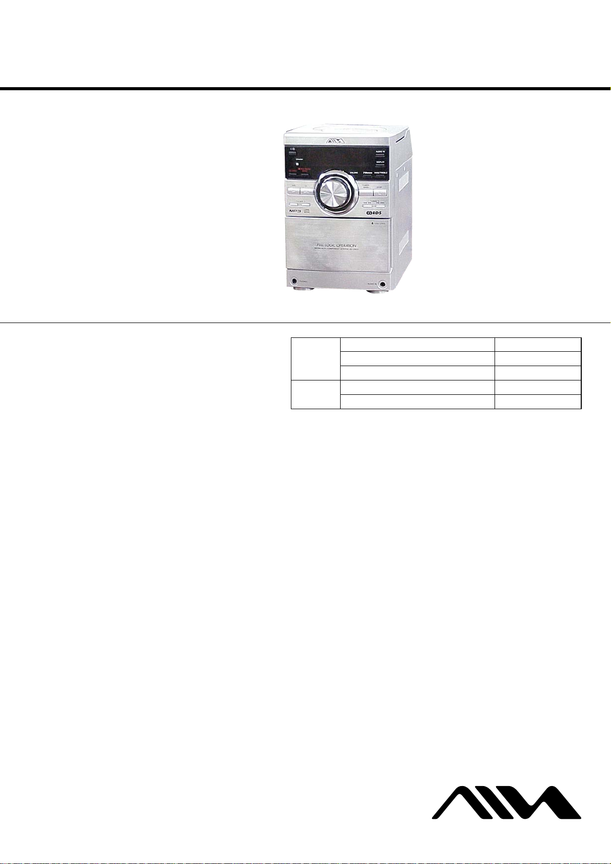
CX-LDB10/LDB20 are the Amplifier, CD player,
Tape Deck and T uner section in XR-DB10/DB20.
Photo : CX-LDB20
CD
Section
Tape deck Model Name Using Similar Mechanism HCD-NE5
Section T ape Transport Mechanism Type CMAL5Z220A
AEP Model
E Model
CX-LDB10/LDB20
Australian Model
CX-LDB10
Model Name Using Similar Mechanism HCD-NE5
Base Unit Name BU-K7BD81B
Optical Pick-up Name KSM-213EDP/C2NP
Amplifier section
CX-LDB20
DIN power output (rated): 35 + 35 W
(6 ohms at 1 kHz, DIN)
Continuous RMS power output (reference):
40 + 40 W
(6 ohms at 1 kHz, 10%
THD)
Music power output (reference):
62 + 62 W
Inputs
AUDIO IN: Sensitivity 700 mV,
impedance 47 kilohms
Outputs
PHONES: Accepts headphones with
an impedance of 8 ohms or
more
SPEAKER: Accepts impedance of 6 to
16 ohms.
CX-LDB10
DIN power output (rated): 20 + 20 W
(6 ohms at 1 kHz, DIN)
Continuous RMS power output (reference):
22.5 + 22.5 W
(6 ohms at 1 kHz, 10%
THD)
Music power output (reference):
38 + 38 W
SPECIFICATIONS
Inputs
AUDIO IN: Sensitivity 700 mV,
impedance 47 kilohms
Outputs
PHONES: Accepts headphones with
an impedance of 8 ohms or
more
SPEAKER: Accepts impedance of 6 to
16 ohms.
CD player section
Laser Diode Properties Emission duration:
continuous
Laser Output*: Less than
44.6 µW
*This output is the value measurement at a distance of
200 mm from the objective lens surface on the
Optical Pick-up Block with 7 mm apert u re)
Frequency response 20 Hz – 20 kHz
Tape deck section
Recording system 4-track 2-channel, stereo
Frequency response 50 – 13,000 Hz (±3 dB),
using Sony TYPE I
cassettes
Tuner section
FM stereo, FM/AM superhe te rodyne tuner
FM tuner section
Tuning range 87.5 – 108.0 MHz
Antenna FM lead antenna
Antenna terminals 75 ohms unbalanced
Intermediate frequency 10. 7 MHz
AM tuner section
Pan-American model: 530 – 1,710 kHz
(with the tuning interval
set at 10 kHz)
531 – 1,710 kHz
(with the tuning interval
set at 9 kHz)
European model: 531 – 1,602 kHz
(with the tuning interval
set at 9 kHz)
Other models: 530 – 1,710 kHz
(with the tuning interval
set at 10 kHz)
531 – 1,602 kHz
(with the tuning interval
set at 9 kHz)
Antenna AM loop ante nna, extern al
antenna terminal
Intermediate frequency 450 kHz
— Continued on next page —
9-879-549-01
2005C1678-1
© 2005.03
MICRO HI-FI COMPONENT SYSTEM
Sony Corporation
Personal Audio Group
Published by Sony Engineering Corporation
Page 2
CX-LDB10/LDB20
General
Power requirements
European model: AC 230 V, 50/60 Hz
Korean model: AC 220 V, 60 Hz
Australian model: AC 230 – 240 V, 50/60 Hz
Mexican model: AC 120 V, 60 Hz
Argentine model: AC 220 V, 50/60 Hz
Other models: AC 110 – 120 V or
220 – 240 V, 50/60 Hz
Adjustable with voltage
selector
Power consumption
CX-LDB20: 95 W
0.3 W (in Power Saving
Mode)
CX-LDB10: 65 W
0.3 W (in Power Saving
Mode)
Dimensions (w/h/d) excl. speakers
Approx. 160 × 230 ×
255 mm
Mass excl. speakers
CX-LDB20: Approx. 4.0 kg
CX-LDB10: Approx. 3.8 kg
Design and specifications are subject to change
without notice.
Notes on chip component replacement
• Never reuse a disconnected chip component.
• Notice that the minus side of a tantalum capacitor may be
damaged by heat.
Flexible Circuit Board Repairing
• Keep the temperature of the soldering iron around 270 °C
during repairing.
• Do not touch the soldering iron on the same conductor of the
circuit board (within 3 times).
• Be careful not to apply force on the conductor when soldering
or unsoldering.
CAUTION
Use of controls or adjustments or performance of procedures
other than those specified herein may result in hazardous radiation
exposure.
This appliance is
classified as a CLASS 1
LASER product. This
label is located on the
rear exterior.
UNLEADED SOLDER
Boards requiring use of unleaded solder are printed with the leadfree mark (LF) indicating the solder contains no lead.
(Caution: Some printed circuit boards may not come printed with
the lead free mark due to their particular size)
: LEAD FREE MARK
Unleaded solder has the following characteristics.
• Unleaded solder melts at a temperature about 40 °C higher
than ordinary solder.
Ordinary soldering irons can be used but the iron tip has to be
applied to the solder joint for a slightly longer time.
Soldering irons using a temperature regulator should be set to
about 350 °C.
Caution: The printed pattern (copper foil) may peel away if
the heated tip is applied for too long, so be careful!
• Strong viscosity
Unleaded solder is more viscou-s (sticky, less prone to flow)
than ordinary solder so use caution not to let solder bridges
occur such as on IC pins, etc.
• Usable with ordinary solder
It is best to use only unleaded solder but unleaded solder may
also be added to ordinary solder.
SAFETY-RELATED COMPONENT WARNING!!
COMPONENTS IDENTIFIED BY MARK 0 OR DOTTED LINE
WITH MARK 0 ON THE SCHEMATIC DIAGRAMS AND IN
THE PARTS LIST ARE CRITICAL TO SAFE OPERATION.
REPLACE THESE COMPONENTS WITH SONY PARTS WHOSE
PART NUMBERS APPEAR AS SHOWN IN THIS MANUAL OR
IN SUPPLEMENTS PUBLISHED BY SONY.
2
Page 3

TABLE OF CONTENTS
CX-LDB10/LDB20
1. SERVICING NOTES ................................................ 4
2. GENERAL ................................................................... 5
3. DISASSEMBLY
3-1. Disassembly Flow ........................................................... 7
3-2. Rear Cabinet .................................................................... 7
3-3. Top Panel Assy, Front Panel Assy ................................... 8
3-4. Base Unit (BU-K7BD81B) ............................................. 8
3-5. Mechanical Deck (CMAL5Z220A) ................................ 9
3-6. CONTROL Board ........................................................... 9
3-7. MAIN Board, Power Transformer................................... 10
3-8. Lid (Cassette) ................................................................. 10
4. TEST MODE ............................................................... 11
5. MECHANICAL ADJUSTMENTS......................... 12
6. ELECTRICAL ADJUSTMENTS .......................... 12
7. DIAGRAMS................................................................. 15
7-1. Block Diagram — CD Section — .................................. 16
7-2. Block Diagram — MAIN Section — ............................. 17
7-3. Printed Wiring Board — CD Board — .......................... 18
7-4. Schematic Diagram — CD Board — ............................. 19
7-5. Printed Wiring Board — MAIN Section (1/2) — .......... 20
7-6. Printed Wiring Board — MAIN Section (2/2) — .......... 21
7-7. Schematic Diagram — MAIN Section (1/3) — ............. 22
7-8. Schematic Diagram — MAIN Section (2/3) — ............. 23
7-9. Schematic Diagram — MAIN Section (3/3) — ............. 24
7-10. Printed Wiring Board — CONTROL Board (1/2) — .... 25
7-11. Printed Wiring Board — CONTROL Board (2/2) — .... 26
7-12. Schematic Diagram — CONTROL Board —................ 27
7-13. Printed Wiring Board — POWER Board — .................. 28
7-14. Schematic Diagram — POWER Board —..................... 29
7-15. Printed Wiring Board — AUX Section — ..................... 30
7-16. Schematic Diagram — AUX Section — ........................ 30
8. EXPLODED VIEWS
8-1. Overall Section ................................................................ 36
8-2. Front Panel Section ......................................................... 37
8-3. Chassis Section ................................................................ 38
8-4. Top Panel Assy ................................................................ 39
9. ELECTRICAL PARTS LIST .................................. 40
3
Page 4

CX-LDB10/LDB20
SECTION 1
SERVICING NOTES
NOTES ON HANDLING THE OPTICAL PICK-UP
BLOCK OR BASE UNIT
The laser diode in the optical pick-up block may suffer electrostatic
break-down because of the potential difference generated by the
charged electrostatic load, etc. on clothing and the human body.
During repair, pay attention to electrostatic break-down and also
use the procedure in the printed matter which is included in the
repair parts.
The flexible board is easily damaged and should be handled with
care.
NOTES ON LASER DIODE EMISSION CHECK
The laser beam on this model is concentrated so as to be focused on
the disc reflective surface by the objective lens in the optical pickup block. Therefore, when checking the laser diode emission,
observe from more than 30 cm away from the objective lens.
LASER DIODE AND FOCUS SEARCH OPERATION
CHECK
Carry out the “S curve check” in “CD section adjustment” and check
that the S curve waveforms is output three times.
MODEL IDENTIFICATION
– Back Panel –
Power voltage
indication
Model Name Power Voltage Indication
Mexican model 120 V AC, 60 Hz
AEP, Russian models 230 V AC, 50/60 Hz
Korean model 220 V A C, 50/60 Hz
Australian model 230 – 240 V AC, 50/60 Hz
Other models
(E51, Singapore, Malaysia and
Argentine models)
110 – 120 V or
220 – 240 V AC, 50/60Hz
4
Page 5
SECTION 2
GENERAL
List of button locations and reference pages
CX-LDB10/LDB20
This section is extracted
from instruction manual.
How to use this page
Use this page to find the location of buttons and other
parts of the system that are mentioned in the text.
Main unit
ALPHABETICAL ORDER
A – H
AUDIO IN 8 (16, 22)
AUDIO IN jack qg (18, 22)
BASS/TREBLE q; (17)
Cassette compartment qj
CD SYNC wa (16)
DISPLAY 9 (14, 20)
Display window 5
FOLDER +/– qk (10, 11, 16)
I – Z
i-Bass 6 (17)
OPEN (CD open/close) 7 (10)
PHONES jack qh
Remote sensor 2
STANDBY indicator ws (20, 23)
TUNER/BAND qa (12, 13)
TUNING +/– qd (12, 13, 17)
VOLUME 4 (18, 22, 23, 25)
Illustration number
r
DISPLAY
RR
Name of button/part Reference page
9 (14, 20)
BUTTON DESCRIPTIONS
?/1 (power) 1 (7, 18, 19, 25)
z REC PAUSE/START 3 (16)
x (stop) qs (10, 16, 25)
.m/M> (skip back/
skip forward, rewind/fast
forward) qd (10, 11, 15)
Z PUSH OPEN (tape open/close)
qf (15)
TAPE/N (play) ql (15)
CD/NX (play/pause) w; (10,
11, 24)
ws
wa
w;
ql
qk
qj
qh
12 3 4 5 67
8
9
q;
qa
qs
qd
qf
qg
5
Page 6
CX-LDB10/LDB20
Remote control
ALPHABETICAL ORDER
A – O P – Z
CD qh (9, 11)
CLEAR qd (11)
CLOCK/TIMER SELECT 2
(18, 19, 23)
CLOCK/TIMER SET 3 (8, 18,
19)
DISPLAY ql (14, 20)
ENTER 9 (8, 11, 12, 18, 19)
EQ qs (17)
FM MODE 4 (14, 24)
FOLDER +/– qa (10, 11, 16)
FUNCTION 6 (22, 25)
PLAY MODE qk (9, 11, 24)
REPEAT 4 (10)
SLEEP w; (17)
TAPE qg (15)
TUNER/BAND 5 (12, 13)
TUNER MEMORY qj (12)
TUNING MODE qk (12, 13)
VOLUME +/– 0 (18, 23)
ql
qk
qj
qh
qg
qf
w;
BUTTON DESCRIPTIONS
?/1 (power) 1 (7, 18, 19, 25)
m/M (rewind/fast forward)
7 (10, 15)
x (stop) 8 (10, 16, 25)
X (pause) 8 (10, 15)
N (play) 8 (9, 11, 19)
+/– (tuning) qf (12, 13)
./> (go back/go forward)
qf (8, 10, 11, 18, 19)
1
2
3
4
5
6
7
qd
qs
qa
8
9
0
Setting the clock
Use buttons on the r emote for the operation.
1 Press ?/1 to turn on the system.
2 Press CLOCK/TIMER SET.
3 Press . or > repeatedly to set the
hour.
4 Press ENTER.
5 Press . or > repeatedly to set the
minute.
6 Press ENTER.
The clock starts working.
To adjust the clock
1
Press CLOCK/TIM ER SE T.
2
Press . or > until “CLOCK” appears,
then press ENTER.
3
Do the same procedures as step 3 to 6
above.
Note
The clock is not displayed in Power Saving Mode
(page 20).
6
Page 7
•This set can be disassembled in the order shown below.
3-2. REAR CABINET
(Page 7)
3-8. LID (CASSETTE)
(Page 10)
3-5. MECHANICAL DECK
(CMAL5Z220A)
(Page 9)
3-7. MAIN BOARD,
POWER TRANSFORMER
(Page 10)
3-6. CONTROL BOARD
(Page 9)
3-4. BASE UNIT
(BU-K7BD81B)
(Page 8)
3-3. TOP PANEL ASSY,
FRONT PANEL ASSY
(Page 8)
SET
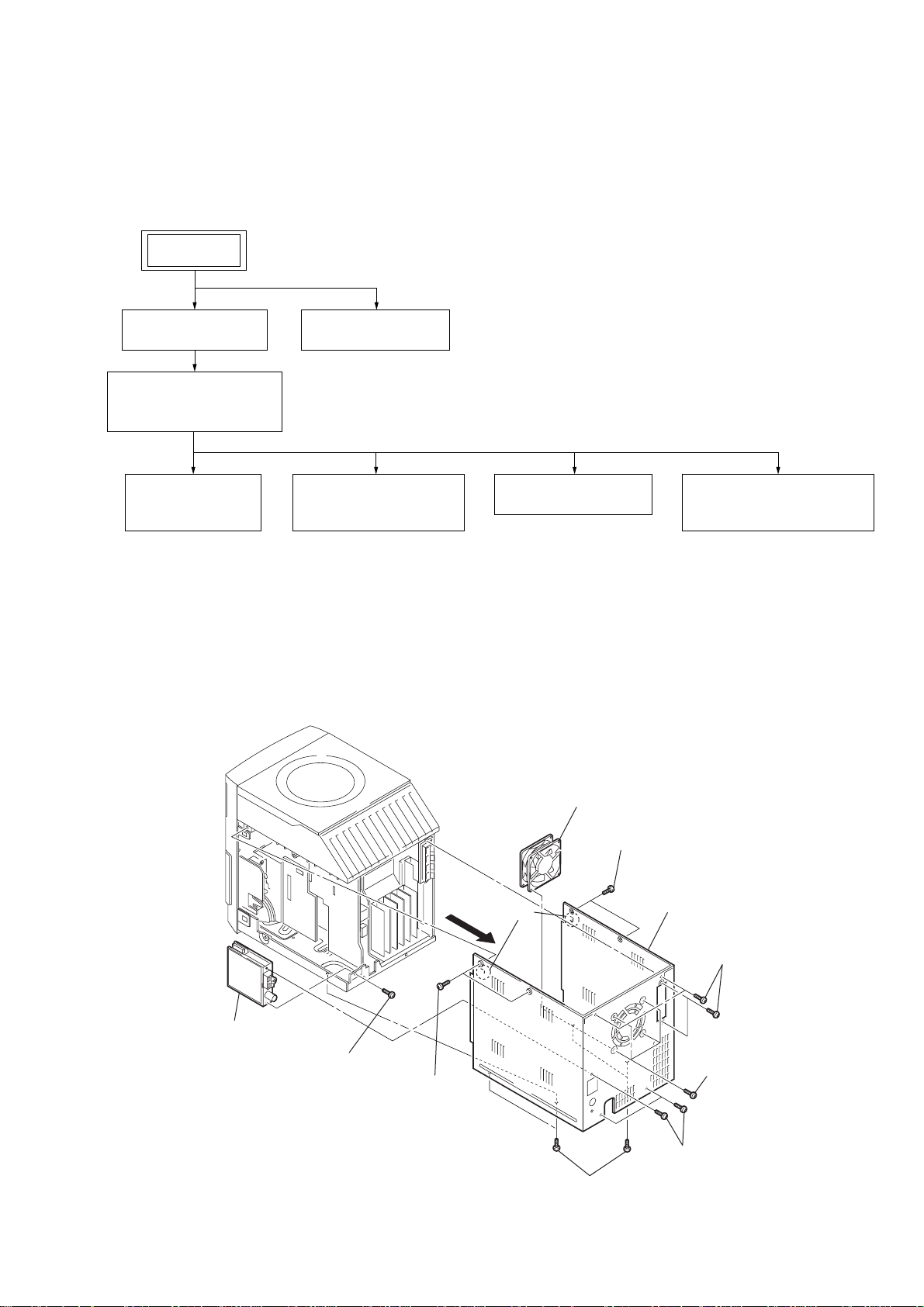
3-1. DISASSEMBLY FLOW
CX-LDB10/LDB20
SECTION 3
DISASSEMBLY
Note: Follow the disassembly procedure in the numerical order given.
3-2. REAR CABINET
qa
AM/FM tuner
0
screw
(BVTP3
8
DC fan
6
two screws
(BVTP3
7
two claws
×
8)
5
two screws
(BVTP3
×
8)
×
8)
9
rear cabinet
2
four screws
×
(BVTP3
4
four screws
(BVTP3
8)
×
8)
1
four screws
(BVTP3
×
3
three screws
(BVTP3
8)
×
8)
7
Page 8

CX-LDB10/LDB20
3-3. TOP PANEL ASSY, FRONT PANEL ASSY
1
qd
connector
(6P)
qj
front panel assy
7
(17core) (CN003)
connector
(2P)
wire (flat type)
qs
qa
earth wire
screw
(BVTP3 × 8)
3
top panel assy
2
wire (flat type)
(27core) (CN004)
4
wire (flat type)
(11core)
qf
two screws
(BVTP3 × 8)
3-4. BASE UNIT (BU-K7BD81B)
qh
claw
9
connector
(3P)(CN101)
q;
wire (flat type)
(23core)
qg
claw
8
connector
(7P)(CN102)
3
two vibration proof rubbers (PNK)
6
5
screw
(BVTP3 × 8)
two earth wires
1
two screws
4
two vibration proof rubbers (GRN)
2
two screws
(+PSW2.6
5
base unit
(BU-K7BD81B)
×
10)
(+PSW2.6
×
10)
8
Page 9

3-5. MECHANICAL DECK (CMAL5Z220A)
1
wire (flat type)
(7core)
5
plate (shield cassette)
CX-LDB10/LDB20
3-6. CONTROL BOARD
1
knob (VOL)
6
mechanical deck (CMAL5Z220A)
3
coating clip
8
CONTROL board
2
three screws
(BVTP2.6
4
two earth wires
×
8)
2
four screws
(BVTP3 × 8)
7
wire (flat type)
(11core) (CN402)
6
wire (flat type)
(7core) (CN404)
4
wire (flat type)
(17core) (CN401)
5
wire (flat type)
(23core) (CN403)
3
seven screws
(BVTP2.6
×
8)
9
Page 10
CX-LDB10/LDB20
3-7. MAIN BOARD, POWER TRANSFORMER
3
two sumitite screws
(B3)
9
2
screw
(BVTP3
4
MAIN board
×
8)
8
four screws
holder (pwb PT)
7
two claws
5
two tapping screws (B3)
6
shield cover
3-8. LID (CASSETTE)
1
connector
(13P)(CN902)
q;
power transformer
10
1
Open the lid cassette.
3
lid cassette
two hooks
2
2
claw
Page 11

SECTION 4
TEST MODE
CX-LDB10/LDB20
COLD RESET
• The cold reset clears all data including preset data stored in
the RAM to initial conditions. Execute this mode when
returning the set to the customers.
Procedure:
1. Press the ?/1 button to turn the set ON.
2. Press three buttons x , ?/1 and [VOLUME] down simultaneously.
3. The message “RESET” is displayed and the set is reset.
TUNER STEP CHANGE
•A step of AM channels can be changed over between 9 kHz
and 10 kHz.
Procedure:
1. Press the ?/1 button to turn the set ON.
2. Select the function “TUNER”, and press [TUNER/BAND]
button to select the BAND “AM”.
3. Press the ?/1 button to turn the set OFF.
4. Press the > and ?/1 buttons simultaneously, and thus
the channel step is changed over.
SHIP RESET
Procedure:
1. Press the ?/1 button to turn the set ON.
2. Press the CD u button to select “CD”
3. Remove the disc.
4. The message “NO DISC” is displayed.
5. Press three buttons x , CD u and [VOLUME] down si-
multaneously.
6. The message “SHIP RESET” is displayed and the set is reset.
The CD function is activated.
7. To e xit from this mode, press the ?/1 button and pull out the
AC plug.
CD Repeat 5 Times Limit Release Mode
Procedure:
1. Press the ?/1 button to turn the set ON.
2. Set the function to “CD”.
3. Press three buttons x , H , and [VOLUME] down simulta-
neously.
4. The repeat all mark blinks and then repeat 5 times limit is
released.
PANEL TEST MODE
•This mode is used to check the software version, LCD, LED
and keyboard.
Procedure:
1. Press the ?/1 button to turn the set ON.
2. Press the CD u button to select “CD”
3. Press three bottons [DISPLAY] , ?/1 and [VOLUME] down
simultaneously.
4. When the panel test mode is activated, all segments are turned
on.
VERSION DISPLAY
•This mode is used check the model, destination, software
version.
Procedure:
1. When the panel test mode is activated, press the button
[BASS/TREBLE], the model and destination are displayed.
KEY TEST MODE
Procedure:
1. When the panel test mode is activated, press the H button,
to select the key test mode.
2. To enter the KEY test mode, the fluorescent indicator displays
“K0 VO”. Each time a button is pressed, “KEY” value
increases. However, once a button is pressed, it is no longer
taken into account. When all keys are pressed correctly, “K15
VO” is displayed.
3. To exit from this mode, pull out the AC plug.
11
Page 12
CX-LDB10/LDB20
)
SECTION 5
MECHANICAL ADJUSTMENTS
SECTION 6
ELECTRICAL ADJUSTMENTS
TAPE MECHANISM DECK SECTION
Precaution
1. Clean the following parts with a denatured alcohol-moistened
swab:
record/playback heads pinch rollers
erase head rubber belts
capstan idlers
2. Demagnetize the record/playback head with a head
demagnetizer.
3. Do not use a magnetized screwdriver for the adjustments.
4. After the adjustments, apply suitable locking compound to
the parts adjusted.
5. The adjustments should be performed with the rated power
supply voltage unless otherwise noted.
Torque Measurement
Mode Torque meter Meter reading
2.94 mN • m to 7.84 mN • m
FWD CQ-102C 31 to 71 g • cm
(0.43 – 0.98 oz • inch)
FWD
back tension
FF/REW CQ-201B 71 to 143 g • cm
FWD tension CQ-403A 100 g or more
CQ-102C 2 to 6 g • cm
0.14 mN • m to 0.59 mN • m
(0.02 – 0.08 oz • inch)
6.86 mN • m to 17.64 mN • m
(0.98 – 1.99 oz • inch)
more than 0.98 N • m
(3.53 oz or more)
DECK SECTION 0 dB = 0.775 V
Precaution
1. Demagnetize the record/playback head with a head
demagnetizer.
2. Do not use a magnetized screwdriver for the adjustments.
3. After the adjustments, apply suitable locking compound to
the parts adjust.
4. The adjustments should be performed with the rated power
supply voltage unless otherwise noted.
5. The adjustments should be performed in the order given in
this service manual. (As a general rule, playback circuit
adjustment should be completed before performing recording
circuit adjustment.)
6. The adjustments should be performed for both L-CH and RCH.
7. Switches and controls should be set as follows unless otherwise
specified.
Test T ape
Tape Signal Used for
P-4-A100 10 kHz, –10 dB Azimuth Adjustment
WS-48B 3 kHz, 0 dB Tape Speed Check
Record/Playback Head Azimuth Adjustment
Procedure:
1. Mode: Playback
test tape
P-4-A100
(10 kHz, – 10 dB)
MAIN board
SPEAKER terminal (J302
L-CH, R-CH
level meter
set
+
–
2. Turn the adjustment screw and check output peaks. If the peaks
do not match for L-CH and R-CH, turn the adjustment screw
so that outputs match within 1dB of peak.
Output
level
within
1dB
L-CH
peak
R-CH
peak
within
1dB
Screw
position
L-CH
peak
Screw
position
R-CH
peak
12
Page 13
CX-LDB10/LDB20
+
–
CD board
TP (RFACO)
TP (VC)
oscilloscope
(DC range)
3. Mode: Playback
MAIN board
test tape
P-4-A100
(10 kHz, – 10 dB)
L-CH
set
R-CH
in phase 45°90°135°180
SPEAKER terminal (J302)
L-CH
R-CH
waveform of oscilloscope
good
oscilloscope
wrong
H
V
°
4. After the adjustments, apply suitable locking compound to
the parts adjusted.
Adjustment Location:Record/Playback/Erase Head
Tape Speed Check
Mode: Playback
test tape
WS-48B
(3 kHz, 0 dB)
set
MAIN board
SPEAKER terminal (J302)
L-CH, R-CH
frequency counter
+
–
CD SECTION
Note:
1. CD Block is basically constructed to operate without
adjustment.
2. Use YEDS-18 disc (3-702-101-01) unless otherwise indicated.
3. Use an oscilloscope with more than 10 MΩ impedance.
4. Clean the object lens by an applicator with neutral detergent
when the signal level is low than specified value with the
following checks.
5. Check the focus bias check when optical block is replaced.
FOCUS BIAS CHECK
Adjustment and Connecting Location: CD board (See page 14)
Procedure :
1. Connect the oscilloscope to TP (RF ACO) and TP (VC) on the
CD board.
2. Insert the disc (YEDS-18). (Part No. : 3-702-101-01)
3. Press the [CD ] button.
4. Confirm that the oscilloscope waveform is as shown in the
figure below. (eye pattern)
A good eye pattern means that the diamond shape (◊) in the
center of the waveform can be clearly distinguished.
• RF signal reference waveform (eye pattern)
VOLT/DIV: 0.2 V (with the 10: 1 probe in use.)
TIME/DIV: 500 ns
NX
1. Insert the WS-48B into the deck.
2. Press the H button on the deck.
3. Confirm that the frequency counter reads 3,000 ± 90 Hz.
Sample value of Wow and Flutter: 0.3% or less W.RMS (JIS)
(WS-48B)
1.1
0.2 Vp-p
When observing the eye pattern, set the oscilloscope
for AC range and raise vertical sensitivity.
13
Page 14
CX-LDB10/LDB20
Checking Location:
– CD BOARD (Conductor Side) –
TP (VC)
TP
(RFACO)
14
Page 15
SECTION 7
DIAGRAMS
CX-LDB10/LDB20
THIS NOTE IS COMMON FOR PRINTED WIRING BOARDS AND SCHEMATIC DIAGRAMS.
(In addition to this, the necessary note is printed in each block.)
For Schematic Diagrams.
Note:
• All capacitors are in µF unless otherwise noted. (p: pF).
50 WV or less are not indicated except f or electrolytics and
tantalums.
• All resistors are in Ω and 1/
specified.
• f : internal component.
• C : panel designation.
Note: The components identified by mark 0 or dotted
line with mark 0 are critical for safety.
Replace only with part number specified.
• A : B+ Line.
• B : B– Line.
• H : adjustment for repair.
•Voltages and waveforms are dc with respect to ground under no-signal (detuned) conditions.
no mark: CD STOP
•Voltages are taken with a VOM (Input impedance 10 MΩ).
Voltage variations may be noted due to normal production
tolerances.
•Waveforms are taken with a oscilloscope.
Voltage variations may be noted due to normal production
tolerances.
• Circled numbers refer to waveforms.
• Signal path.
F : TUNER
J : CD PLAY
E : T APE PLAY
j : TAPE REC
f : AUX IN
•Abbreviation
AUS: Australian model
AR : Argentine model
E51 : Chilean and peruvian models
KR : Korea model
MX : Mexican model
MY : Malaysia model
RU : Russian model
SP : Singapore model
4
W or less unless otherwise
For Printed Wiring Boards.
Note:
• X : parts extracted from the component side.
• Y : parts extracted from the conductor side.
• W : indicates side identified with part number.
• f : internal component.
• : Pattern from the side which enables seeing.
(The other layers' patterns are not indicated.)
Caution:
Pattern face side : Parts on the pattern face side seen from
(Conductor side) the pattern face are indicated.
Parts face side : Parts on the parts face side seen from
(Component side) the parts face are indicated.
• Indication of transistor.
C
Q
B
E
B
These are omitted.
Q
CE
These are omitted.
• Circuit Boards Location
MAIN board
CD board
CONTROL board
POWER (1) board
HEADPHONE board
TUNER unit
POWER (2) board
AUX board
CX-LDB10/LDB20
1515
Page 16
CX-LDB10/LDB20
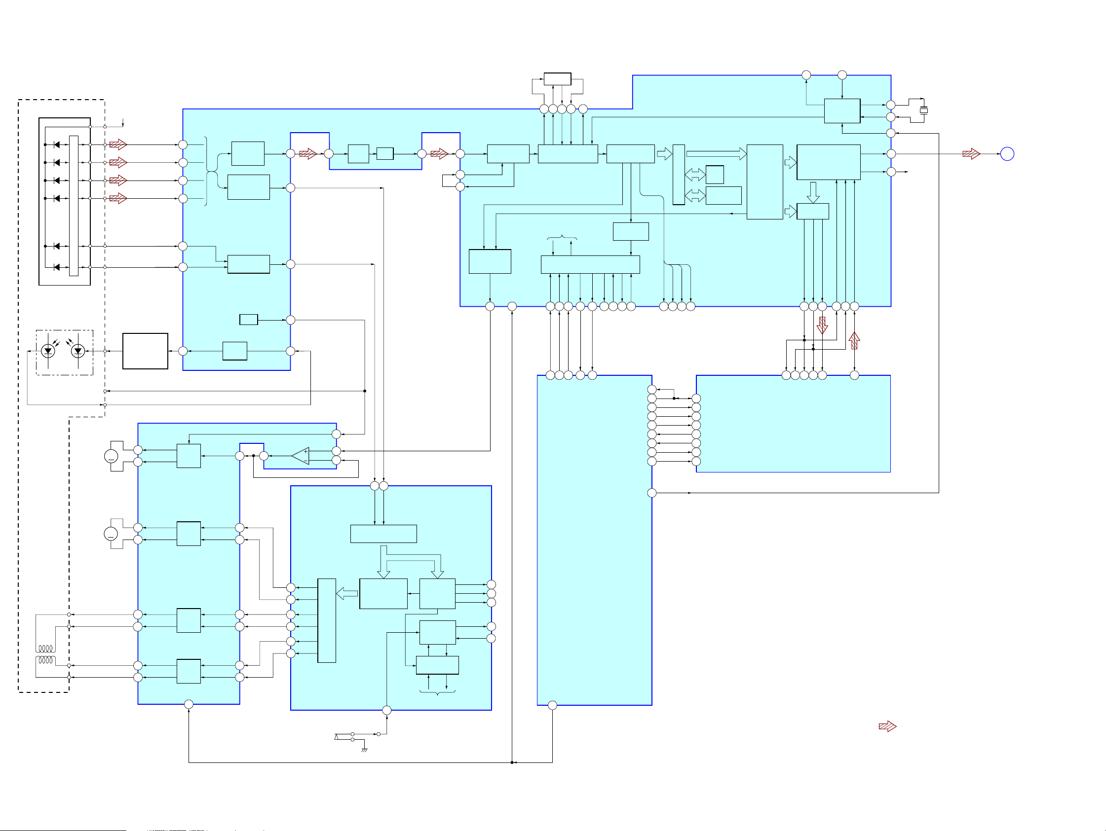
7-1. BLOCK DIAGRAM — CD SECTION —
DETECTOR
A
B
C
D
F
E
OPTICAL PICK-UP
BLOCK
(KSM-213EDP)
LASER DIODE
PD
I-V AMP
LD
VC
M101
(SPINDLE)
M
D +3.3V
AUTOMATIC
POWER
CONTROL
Q10
CH4OUTF
16
CH4OUTR
15
A
26
B
27
C
28
D
29
F
20
E
19
LD
36
MOTOR/COIL DRIVE
IC251
MOTOR
DRIVE
CH4IN
SUMMING
AMP
FOCUS
ERROR
TRACKING
ERROR AMP
APC LD
AMP
24
RF
AMP
VC
FILTER
CD DSP
IC101 (1/2)
OPIN+
OPIN-
EG
IN
RFAC
35
VCA
26
2
1
RFACO
EQ
41
42
45
46
RFACI
ASYI
ASYO
DIGITAL
CLV
PROCESSOR
MDP
6
ASYMMETRY
CORRECTOR
100
AC_
SUM
34
FEO
24
TEO
22
VC
25
PD
37
OUTVREF
OPOUT
27
XRST
51 53
FILI
PCO
FILO
CLTV
DIGITAL PLL
TO SERVO AUTO
SEQUENCER
CPU INTERFACE
DATA
CLOCK
XLAT
27
29 100
XLT
CD-CLK
CD DATA
1125052
XPCK
DEMODULATOR
SUBCODE
PROCESSOR
SQSO
EXCK
SCOR
SENS
SBSO
96 97
98 99115107102 105 104 110 111
SCOR
MI-DIO-I
MI-DIO-O
MP3-REQ
MP3-STB
MP3-RST
SENS
EFM
SQCK
MI-CK
MI-CS
MI-LP
MI-ACK
32K
RAM
INTERNAL BUS
WFCK
XUGF
GFS
113
25
26
24
4
5
1
3
6
2
CORRECTOR
EMPH
68
MIDIO
6
MICK
7
MICS
4
MILP
5
MIACK
8
PO11/BUCK/AD14
36
STANDBY
3
RESET
2
ERROR
MP3 DECODER
IC301
D/A
DIGITAL
INTERFACE
117 93
C4M
SELECTOR
LRCK
63 66 65
16
19
18 14
SBSY/BCKIB
SFSY/LRCKIB
D/A
CONVERTER
BCK
PCMD
15
SDI0
BCKIA
LRCKIA
XTSL
CLOCK
GENERATOR
LRCKI
BCKI
62 60 61
PCMDI
1128 19
SDO0
XTAO
XTAI
XTACN
AOUT1
AOUT2
77
78
95
81
86
R-CH
X171
16.9344MHz
CD
MAIN
A
Section
2-AXIS
DEVICE
(TRACKING)
(FOCUS)
M102
(SLED)
21 23
CD DSP
IC101 (2/2)
CH3OUTF
17
M
18
14
13
12
11
CH3OUTR
CH1OUTF
CH1OUTR
CH2OUTF
CH2OUTR
MOTOR
DRIVE
DRIVE
DRIVE
MUTE
COIL
COIL
20
CH3FIN
CH3RIN
CH1FIN
CH1RIN
CH2FIN
CH2RIN
23
22
SFDR
9
SRDR
10
4
5
6
7
TFDR
11
TRDR
12
FFDR
13
FRDR
14
PWM GENERATOR
FOCUS/TRACKING/SLED
S101
(LIMIT)
FEI
TEI
A/D
CONVERTER
FOCUS/
TRACKING/SLED
SERVO DSP
SSTP
7
MIRR,
DFCT, FOK
DETECTOR
SERVO
INTERFACE
SERVO AUTO
SEQUENCER
TO CPU INTERFACE
FOK
MIRR
DFCT
COUT
SCLK
SYSTEM CONTROLLER
IC401 (1/2)
3
1
2
119
108
X-RST
95
XTCN
94
• R-ch is omitted due to same as L-ch.
• Signal Path
: CD PLAY
CX-LDB10/LDB20
1616
Page 17

7-2. BLOCK DIAGRAM — MAIN SECTION —
CX-LDB10/LDB20
LDB20
CD SERVO
Section
ANTENNA
(REC/PB/ERASE)
TAPE MECHANISM
DECK BLOCK
MOTOR 9V
MM
(CAPSTAN/REEL)
(DECK-A)
J702
AUDIO IN
CD
A
FM 75Ω
COAXIAL
AM
L-CH
R-CH R-CH
HRPE
ERASE
SOL 9V
PACK
R RFC
PLAY SW
END SW
FLUORESCENT
INDICATOR TUBE
REMOTE CONTROL
CAPSTAN/REEL
MOTOR DRIVE
FL401
RECEIVER
IC402
Q404,405
PLUNGER
DRIVE
Q402,403
FM/AM TUNER PACK
FM ANT
TU LCH
TU RCH
ANT GND
TU DI
AM ANT
TU DO
TU CL
ANT GND
TU CE
TUNED
STEREO
MUTE
RDS DATA
RDS CLOCK
79
TA MO
78
TA SOL
83
TA-SW
TA PLAY SW
82
TA END SW
81
53-59
43-51,
31 – 42
RMC_IN
7
R-CH
REC/PB
SWITCH
Q101,103,
252-254
S1 – 16
G1 – G12
R-CH
CLK
TUNED
STEREO
TU-MUTING
RDS DATA
RDS CLOCK
POWER
AUX-L
19
18
OUT-L
CD-L
21
R-CH
AMP
IC301
15
+INA
11
+INB
OUTA
OUTB
7
5
LDB10
J701
PHONES
RY351
RELAY
SW
Q356
J701
PHONES
+
TUNER-L
23
DO
DI
CE
TAPE-L
2
BIAS OSC
T251
DI
CE
DO
CLK
TUNED
STEREO
RDS DATA
RDS CLOCK
77
75
73
72
TU DI
TU CE
TU CLOCK
71
TU TUNED
TU STEREO
80
18
RDS-CLK
RDS-DATA
76
TU DO
INPUT SELECT,
ELECTRICAL VOLUME
IC101
28
REC-O-L
CONT
13
REC BIAS
SWITCH
Q256,257
BIAS OSC
Q255
TU-MUTING
70 87
TU MUTE
21
22
TA RP
O-VOL LED
91
LED DRIVE
Q407
D410-415
VOLUME
TA BIAS
LED DRIVE
(STANDBY)
B +10V
30
F-DATA
SYSTEM CONTROLLER
IC401 (2/2)
ST-BY LED
88
Q408
D416
S401-415
(FRONT PANEL KEYS)
X402
X401
O-XT2
16MHz
15 13
I-XT1
XOUT
S820
ROTARY
ENCODER
RV401
32.768kHz
11 10
(CD LID OPEN/CLOSE DETECT)
VOLUME
D420
XIN
69 CD OPEN
97 VOL_ENCODER
74
ST-BY
13
MUTE
Q355
+
85
AMP MUTE
KEY WAKE UP
KEY0,
KEY1
89,90
TH351
OVER
HEAT
DET
Q354
-35V
DETECT
Q001,002,017
DETECT
Q003,004
+
AC
+14V
DC
I-POWER_MONITOR
D002
CD +1.5V
AMP B+
AMP B–
92CD ON
20I_POWER_DOWN
12RESET
86POWER ON
FAN B+
SW
Q603-605
MUTE
Q606
+1.5V
REGULATOR
IC303
CD +3.3V
RESET SWITCH
+
M +7V
+3.3V(MAIN)
SYS +3.3V
SYS +3.3V
Q401
MUTE
Q019
D602
L : POWER ON
DC DET
Q050,051
REGULATOR
Q011,012
VM +10V
+3.3V
+
–
+
–
FAN MOTOR
Q601,602
M+PV
+3.6V
VOLTAGE
DETECT
DRIVE
D408
IC403
L
R
+3.6V
Q005
J302
SPEAKER
IMPEDANCE
USE 6 – 16Ω
+3.3V
REGULATOR
D012,015
AEP
FAN
TO
POWER AMP
TO
FLUORESCENT
INDICATOR TUBE
+3.3V
REGULATOR
Q018
M+7V
REGULATOR
Q010
SWITCH
Q409
L : POWER ON
LDB20
LED+B
D009
D011
+14V
Q901-904
AMP B+
AMP B–
AC 3.6V
FL –29V
+10V
REGULATOR
IC003
+3.9V
REGULATOR
Q007-009
Q603-605
AC DET
FAN B+
SW
MUTE
Q606
–29V
–29V
REGULATOR
REGULATOR
Q013-016
Q013-016
SUB B+
+10V
REGULATOR
IC002
+
D602
L : POWER ON
D905
RECT
D901,902
RECT
D903,904
RECT
D907-910
RECT
D914,916
D912
-35V
MAIN POWER
TRANSFORMER
D911
RECT
SUB POWER
TRANSFORMER
VM+10V
SUB B+
+
L
–
+
R
–
FAN MOTOR
DRIVE
Q601,602
T902
T901
D006
J302
SPEAKER
IMPEDANCE
USE 6 – 16Ω
FAN
(EXCEPT SP, MY, E51)
(SP, MY, E51)
VOLTAGE
SELECTOR
S901
(EXCEPT SP, MY, E51)
MAIN POWER
RELAY DRIVE
Q006
L : POWER ON
• R-ch is omitted due to same as L-ch.
• Signal Path
: TUNER
: CD PLAY
: TAPE PLAY
: REC
: AUX IN
RY901
(AC IN)
CX-LDB10/LDB20
1717
Page 18

CX-LDB10/LDB20
7-3. PRINTED WIRING BOARD — CD BOARD —
12
34567 9
A
CD BOARD
(COMPONENT SIDE)
B
C302
C
C303
D
E
FB301
F
R205
G
R201
C201
C203
C318
C184
C183
C182
C209
C305
R313
C315
C316
R302
C314
C312
C210
R162
R171
C174
R191
R173
C172
R172
R165
X171
H
C151
C134
I
• See page 15 for Circuit Boards Location. :Uses unleaded solder.
8
C255
R253
C116
C17
1-861-619-
C260
12
(12)
C171
R405
C308
C196
R354
R351
R121
C123
R352
R353
C195
C125
C15
C10
C11
C16
C258
C259
Q10
C18
E
C257
C14
R11
R12
R13
R10
10
CD BOARD
(CONDUCTOR SIDE)
C252
28 22 1521
IC251
17 148
R252
R251
C251
C114
TP
(VC)
R113
C113
R114
C112
C111
(KSM-213EDP/C2NP)
11
R112
OPTICAL
PICK-UP
BLOCK
CN101
R111
C115
C320
12
M
M101
(SPINDLE)
13 15
14
13
16
17
IC303
116
R163
R143
C313
C212
C143
R141
R419
64
49
C142
C311
R409
C211
90
61
R142
C181
C162
54
C141
R306
C194
C161
R403
R408
R412
R203
R401
R406
R151
R301
R182
R402
C213
R161
C317
R305
R410
M102
M
(SLED)
CN201
1
C186
C185
R181
27
R204
1-861-619-
(Page 21)
12
(12)
A
MAIN
BOARD
CN004
S101
(LIMIT)
R404
17
32
TP
C124
C306
IC301
R303
R407
IC101
R132
R131
C163
C133
R133
4833
C310
C132
C131
R307
C307
C309
R411
120 91
1
30
31 60
C122
(RFACO)
J
CX-LDB10/LDB20
• Semiconductor
Location
Ref. No.
IC101 G-13
IC251 D-10
IC301 D-13
IC303 B-14
Q10 F-7
Location
1818
Page 19

CX-LDB10/LDB20
7-4. SCHEMATIC DIAGRAM — CD BOARD —
R307
C307
10k
0.1
WE/SDO1
SDO2
CS/RAS/
PIO7/BUS3/IO7
PO12
AD15/CAS/
C314
TP433
MP3VDD
SDO3/OE
PO9/AD12
PO08/AD11
VDDM
SRMSTB
VDDT
AD10
AD9
AD8
PO07/AD7
PO06/AD6
PO05
AD5/
AD3/PO03
AD4/PO04
C312C313
47
4V
C311 C309
0.1 0.1
0.10.1
C302 C303
0.1 0.1
MP3REQ
R303
100k
C310
0.1
FB301
PIO2/IO2
PIO3/IO3
PIO1/SDI3/IO1
PIO4/FI1/BUS0/IO4
PIO5/FI2/BUS1/IO5
PIO6/FI3/BUS2/IO7
PO11/BUCK/AD14
PO10/CCE/AD13
MP3 DECODER
IC301
TC94A34FG-002
CKO/PO13/AD16
VDD
VSS
AD0/PO00
AD1/PO01
AD2/PO02
C308
47
4V
GND
STBY
NC
VOUT
C305 TP422
220
4V
VSS
PIO0/SDI2/IO0
XO
VDDX
R306
0
VIN
IRQ/FIO
CKI/CLOCK/
XI
+1.5V REGULATOR
TXO
VDD
TEST
VSSX
IC303
BH15FB1WG
SFSY/LRCKIB
MIMD
MP3GND
• See page 32, 33 and 34 for IC Block Diagrams. • See page 31 for Waveforms.
R203
0
SDI1/
DATA
SBSY/BCKIB
VCOI
VSSP
STANBY
R313
220
LRCKIA
BCKIA
LRCKO
MIACK
MIDIO
RESET
SDI0
BCKO
SDO0
VSS
VDDT
MICK
MILP
MICS
VDDP
C316C315
0.00220.1
R351
100
0.1
C306
100
R405
MIACK
100
R404
MICK
MIDIO
100
R419
R403
R402
R401
R301
100k
R305
100k
C317
0.01
MILP
100
MICS
MP3STB
100
MP3RST
100
C318
0.01
R354
100
R352
100
R353
100
10k
R302
C161
0.1
C181
0.1
0
R173
C185
470p
C182
0.1
C186
470p
C201
100
10V
TP427
PCMDI
TP103
LRCK
TP104
PCMD
TP105
BCK
DOUT
R161
100
C171 R171
22p 470
R172
C172
27p
AOUT1
AOUT2
1M
C183
R181
22
100
6.3V
C184
R182
22
100
6.3V
C203
C162
100
0.1
10V
C174X171
BCKI
PCMDI
LRCKI
LRCK
VSS
PCMD
BCK
VDD
EMPH
EMPHI
IOVDD2
DOUT
TEST
TEST1
IOVSS2
NC
0.116.9344MHz
XVSS
XTAO
XTAI
XVDD
AVDD1
AOUT1
VREFL
AVSS1
AVSS2
VREFR
AOUT2
AVDD2
NC
IOVDD0
RMUT
LMUT
100p
AVSS3
DATA
C133
0.01
R133
180k
R132
10k
VCTL
VPCO
CXD3059AR
VSS
XLAT
C196
0.1
C131
C125 R121
R131C134
1M0.1
0.1 15k
TP125
RFACI
TP124
RFACO
0.47
C132
BIAS
ASYI
ASYO
RFACI
RFACO
AVDD3
CD DSP
IC101
WFCK
ATSK
SCLK
SENS
VDD
CLOCK
R191
0
330p
C124
AVSS4
XUGF
C122C123
0.10.1
LD
NC
PD
RFC
EG_IN
VDD
SCOR
C2PO
GFS
XPCK
AC_SUM
C4M
PDSENS
WDCK
RFDCO
COUT
AVSS0
AVDD0
IOVDD1
TRDR
SRDR
IOVSS1
AVDD4
FRDR
FFDR
TFDR
SFDR
SSTP
MDP
LOCK
DFCT
MIRR
NC
NC
D
C
B
A
VC
FEO
FEI
TEO
TEI
F
E
NC
VSS
FOK
C142
1500p
C151
100
10V
R151
0
NC
DDCR
AVSS5
IOVSS0
XTSL
NC
R165
0
R143
C143
3.3k
0.1
C141
0.1
R141
4.7k
1k
R142
FILI
PCO
FILO
CLTV
AVDD5
DDVRSEN
DDVROUT
SYSM
XRST
EXCK
SBSO
SQCK
SQSO
XTACN
R162
47k
C210
0.1
100
0.1
C194
0.1
R163
C163
JPO10 R11
APC 0
R111
JPO102
R113
JPO103
TP425
TP432
TP428
TP429
TP430
TP431
TP423
IOP1
C17
220
4V
1k
1k
AUTOMATIC
CONTROL
C18
1000p
R112
FEI
TEI
R114
FRDR
FFDR
TRDR
TFDR
SW+
MDP
C16R12
Q10
2SA2119K
POWER
15k
15k
R13
R10
1100k
3.3
C111
C112
C113
C114
C115
0.1
3300p
3300p
C10
C15
10
1
TP424
IOP2
D
C
B
A
470p
470p
F
E
FRDR
FFDR
TRDR
TFDR
SRDR
SFDR
MDP
0.1
E
C11
10
D
A
B
C
F
TP102
F+
C14
0.1
C116
C195
0.1
F-
100
10V
VC
TP177
VC
VCC
TP10
TP11
TP12
TP13
TP14
E
E
D
D
A
A
B
B
C
C
F
F
AGND
LD
VR
PD
TP15
PD
F+
TP16
F+
T+
TP17
F-
T-
TP18
T-
F-
TP19
F-
CN101
16P
TP426
SW-
S101
(LIMIT)
/C2NP
MAIN BORAD(3/3)
CN004
(Page 24)
CN201
27P
M+7V
MGND
MGND
MP3STB
MP3REQ
MIACK
MICK
MIDIO
MILP
MICS
MP3(3.3V)
MP3RST
MP3GND
SCOR
SENS
CLK
XLT
DATA
XRST
XTCN
AVDD(3.3V)
ROUT
AGND
LOUT
DGND
DOUT
DVDD(3.3V)
TP402
TP403
TP405
TP408
TP415
TP414
TP186
TP187
TP401
TP404
TP406
TP407
TP417
TP416
TP413
TP412
TP419
TP434
TP410
TP411
TP409
XRST
XTACN
MVDD
MGND
MP3STB
MP3REQ
MIACK
MICK
MIDIO
MILP
MICS
MP3RST
R205
0
SCOR
SENS
CLK
XLT
DATA
XRST
XTCN
AVDD
ROUT
LOUT
DOUT
R204
MP3STB
MP3REQ
MIACK
MICK
MIDIO
MILP
MICS
MP3RST
100
R411
R410
R409
R408
R407
R406
R412
SCOR
CLOCK
XTACN
C212
SENS
22p
XLT
C211
DATA
220p
XRST
AOUT2
AOUT1
DOUT
100
100
100
100
100
100
TP435
C213
22p
C320
0
DVDD
AVDD
AGND
DGND
TP420
TP436
R201
TP421
C209
0.01
DATA
SENS
CLOCK
XLT
MDP
MOTOR/COIL
DRIVE
IC251
BA5947FM-E2
SCOR
R253TP418
10kGAIN_SW
JPO004C251R252R251
MDP6800p22k10k
OPIN-
OPIN+
OPOUT
PREVCC
TFDR
SW
OUTVREF
TRDR
CH1FIN
CH4CAPA
CH1RIN
CH4IN
FRDR
FFDR
CH2FIN
CH2RIN
CH3FIN
CH3RIN
SFDR
SRDR
C259
0.1
F+T+T+T-T-
F-
C258
0.1
C257
0.1
GND
CNF4
POWVCC
CH2OUTF
CH1OUTR
CH2OUTR
MUTE
GND
POWVCC
CH3OUTR
CH3OUTF
CH4OUTF
CH1OUTF
CH4OUTR
C252
0.1
C255
0.1
C260
220
10V
TP250
TP251
TP252
TP253
SP-
SP+
SL+
SL-
M101
(SPINDLE)
M102
(SLED)
CX-LDB10/LDB20
1919
Page 20

CX-LDB10/LDB20
7-5. PRINTED WIRING BOARD — MAIN SECTION (1/2) —
12
34567 9
A
MAIN BOARD
(SIDE A)
B
C
• See page 15 for Circuit Boards Location. :Uses unleaded solder.
8
10 12
11
• Semiconductor
Location
Ref. No.
D010 F-4
D255 E-3
Q006 H-6
Q009 H-6
Q010 C-6
Q011 C-8
Q018 C-8
Q255 D-2
Q257 F-3
Q601 B-11
Q603 I-8
Location
D
E
F
G
LDB20
AEP
H
I
CX-LDB10/LDB20
1-865-483-
2020
Page 21

CX-LDB10/LDB20
7-6. PRINTED WIRING BOARD — MAIN SECTION (2/2) —
A
12
MAIN BOARD
FAN
CN601
34567 9810 12
(SIDE B)
B
C
LDB20
D
E
F
HEADPHONE
BOARD
CN701
(Page 30)
LDB20
W101
• See page 15 for Circuit Boards Location. :Uses unleaded solder.
A
CD
BOARD
CN201
(Page 18)
CN004
B
CONTROL
BOARD
CN401
(Page 26)
CN003
MX
CN002
IC101
CN101
11
C
AUX
BOARD
W702
(Page 30)
DECK
R/P HEAD L. CH
R/P HEAD R. CH
E. HEAD
• Semiconductor
Location
Ref. No.
D002 I-5
D006 H-7
D008 H-7
D009 G-8
D011 F-7
D012 F-10
D013 C-4
D014 D-4
D015 F-9
D017 C-7
D018 C-5
D019 H-8
D023 I-5
D024 I-6
D025 C-5
D026 G-6
D027 G-6
D201 G-2
D202 F-2
D251 C-8
D252 C-9
D253 D-8
D254 B-11
D353 D-6
D354 C-3
D355 H-2
D356 H-2
D358 E-2
D359 E-2
D601 C-3
D602 B-3
D603 I-4
D604 I-5
D605 D-6
Location
F
G
H
AEP
LDB20
(CHASSIS)
CN001
IC002
1-865-483-
IC301
W103
EXCEPT AEP, RU
E
POWER (2)
BOARD
W901
(Page 28)
D
CONTROL
BOARD
CN403
(Page 26)
REG BOARD
IC003
W104
I
(CHASSIS)
1-867-118-
IC002 F-7
IC003 I-11
IC101 C-9
IC301 G-3
Q001 I-5
Q002 I-5
Q003 G-7
Q004 H-7
Q005 I-7
Q007 H-8
Q008 I-8
Q012 C-5
Q013 H-8
Q014 H-8
Q015 I-8
Q016 I-8
Q017 I-6
Q019 H-7
Q050 C-6
Q051 C-6
Q101 C-11
Q102 C-11
Q103 C-11
Q104 C-11
Q201 G-2
Q202 F-2
Q252 B-11
Q253 B-11
Q254 B-11
Q256 F-11
Q353 H-2
Q354 H-3
Q355 D-6
Q356 C-3
Q602 B-3
Q604 I-4
Q605 I-4
Q606 I-4
CX-LDB10/LDB20
2121
Page 22

CX-LDB10/LDB20
7-7. SCHEMATIC DIAGRAM — MAIN SECTION (1/3) —
C
AUX BOARD
W702
(Page 30)
• See page 35 for IC Block Diagram.
MAIN BOARD (1/3)
CN101
3P
CN102
7P
0
0 0 0 0 0 0 0 0 0 0 0
0
*2 C131, C132
220p : EXCEPT MX
0.002 : MX
*2
*2
20
19
18
0
0
IC B/D
IC101
INPUT SELECT,
0 0 0 0 0 0 0 0 0 4 0.5 -4.40
-TE-17
UDZSTE-174.3B
2.7
0
0
0
0
2.7
TE-17
2.7
0
3.1
0
3.1
0
3.1
TP-1EFTP-1EF
Q101-Q103
Q252-Q254
-T2B
REC/PB
SWITCH
-T2B
-TP-7
3.1
3.1
0
3.1
3.1
-TE1
ELECTRICAL
VOLUME
UDZSTE-174.3B
16
17
15
14
5
2
MAIN BOARD
(2/3)
(Page 23)
CX-LDB10/LDB20
1 2 3
4 5
6 7 8
9 10
11 12 13
1
MAIN BOARD
(3/3)
(Page 24)
2222
Page 23

7-8. SCHEMATIC DIAGRAM — MAIN SECTION (2/3) —
IC003
+10V REG
CX-LDB10/LDB20
REG BOARD
2
MAIN BOARD
(1/3)
(Page 22)
FAN +B
SWITCH
-TP-1
-TP-1
-TP-1
LDB20
0.2
0
0
1SS355TE-17
0.1
15.5
2SC4154TP-1EF
RELAY SWITCH
SPEAKER
HEADPHONE BOARD
FAN
CN701
(Page 30)
F
W101
*1
*1
*1
*1
*1
0
TE-1EF
Q601,602
FAN MOTOR
DRIVE
*1
0
6.7
11.8
11.5
TE-17
-AT
11.9
12.4
12.4
12.4
EXCEPT
MX
MX
R609
22
47
R612
1k
470
R613
1k
470
R614
1k
470
R615
1k
470
R616
1k
220
-AT
*1
CN601
3P
MAIN BOARD (2/3)
*
*
STK433-060 : LDB20
STK433-040 : LDB10
LDB10
LDB20
LDB10 LDB20
IC301
POWER AMP
20
19
18
TE-17
17
16
15
14
3.2
0.4
9.9
2.6
TE-17
-0.5
4.8
T106-RR
9.9
2.6
MUTE
T106-RR
3.2
4.8
-0.5
MUTE
TE-17
30.5
8.6
9.2
8.6
30.5
15.7
T106-RR
-30.4 -30.5
10
T106-RR
OVER HEAT DET
9.3
10
8.69.2
T106-RR
9.3
9.2
TE-17
9.2
3.2
TE-17
TE-17
TE-17
Q603-605
2.6
2.6
TE-17
CX-LDB10/LDB20
TP-1EP
1.8
1.8
1.8
TP-1EP
DC DETECT
5
21 22 23
DC DETECT
0.7
0
1.8
TP-1EF
DC DETECT
0
MAIN BOARD
(3/3)
3
(Page 24)
TE-17
UDZS-TE17
-12B
24 25 26
28 29 30 313233
27
35
36
34
37 38
2323
Page 24

CX-LDB10/LDB20
7-9. SCHEMATIC DIAGRAM — MAIN SECTION (3/3) —
MAIN BOARD (3/3)
MAIN BOARD
(1/3)
1
(Page 22)
1 2 3 4 5 6 7 8
9.3
9.3
-AT
BIAS OSC
9
2.1
9.3
-TP-1
REC
BIAS
SWITCH
9.3
TP-EF
10
SWITCH
REC
BIAS
10
MAIN BOARD
(2/3)
3
(Page 23)
10
9
11 12 13
1.7
0
0
-TP-1
AC DETECT
AEP
UBZSTE-173.3B
TE-17
AC DETECT
21
2.5
1.7
TE-17
TE-17
0
IC002
+10V REG
10
2.5
LDB20
22 23 24 25
3.9
1.3
8
0.7
-AT
MUTE
TE-1
0
UDZSTE-175.1B
3.6
3.6
3.6
16
ATP-EF
+3.3V REG
2.8
4.1
+3.3V REG
TE-17
UDZSTE-173.9B
ATP-EF
3.3
0
0.5
TP-1EF TP-1EF
+3.9V
REG
10
-AT
+3.3V REG
M+7V REG
10
7
MX
7.5
UDZSTE-177.5B
3.9
-AT
3
+3.9V
REG
1.3
0.6
1.3
+3.9V
REG
-AT
7
T106-RR
DC DET
7
T106-RR
DC DET
7.7
7.7
7.7
26 27
29 30 31 32 33 34 35
28
36
37 38
EXCEPT
AEP, RU
AEP, RU
CN001
13P
CN002
POWER (2) BOARD
-46.7
-49
-34.5
-28.9
-28.9
Q013-Q016
-29V REG
-28.9
-29.5
CN003
23P
D
CONTROL BOARD
CN403
(Page 27)
17P
B
CONTROL BOARD
CN401
(Page 27)
CN004
27P
A
CD BOARD
CN201
(Page 19)
-49
-34.5
-31.5
-40.9
W901
E
(Page 29)
CX-LDB10/LDB20
2424
Page 25

CX-LDB10/LDB20
7-10. PRINTED WIRING BOARD — CONTROL BOARD (1/2) —
12
CONTROL BOARD (SIDE A)
A
B
C
STANDBY
I/1
• See page 15 for Circuit Boards Location. :Uses unleaded solder.
34567 9
8
AUDIO IN
• Semiconductor
Location
Ref. No.
D410 E-4
D411 E-4
D412 E-4
D413 E-6
D414 E-6
D415 E-6
D416 C-2
Q402 F-5
Q404 F-5
Location
D
E
F
CD SYNC
TAPE
FOLDER –
zREC
PAUSE/START
FOLDER +
CD
LDB20
VOLUME
LDB20
i-BASS
TUNER/BAND
TUNING – TUNING +
BASS/TREBLE
DISPLAY
STOP
CX-LDB10/LDB20
1-865-484-
2525
Page 26

CX-LDB10/LDB20
7-11. PRINTED WIRING BOARD — CONTROL BOARD (2/2) —
A
12
CONTROL BOARD (SIDE B)
34567 9810
CD DOOR
OPEN/CLOSE
B
C
• See page 15 for Circuit Boards Location. :Uses unleaded solder.
(FLUORESCENT INDICATOR TUBE)
W401
LDB20
FL401
IC401
LDB20
• Semiconductor
Location
Ref. No.
D403 E-9
D404 D-8
D405 D-8
D406 G-6
D408 F-10
D409 B-9
D418 F-4
D419 F-3
D420 C-5
IC401 C-7
IC402 C-9
IC403 D-8
Q401 E-8
Q403 F-6
Q405 G-5
Q407 E-4
Q408 B-10
Q409 E-9
Location
D
E
F
B
MAIN
BOARD
CN003
(Page 21)
CN401
CN402
LDB20
LDB20
LDB20
CN404
IC403
IC402
CN403
G
CX-LDB10/LDB20
(CHASSIS)
TUNER PACK TAPE DECK
2626
D
1-865-484-
MAIN
BOARD
CN002
(Page 21)
Page 27

CX-LDB10/LDB20
7-12. SCHEMATIC DIAGRAM — CONTROL BOARD —
CONTROL BOARD
CD DOOR
OPEN/CLOSE
LDB20
470
470
470
470
3.4
0
00
0.7
0
-TP1
LED DRIVE
FOLDERFOLDER
TUNING
TUNING
i-BASS
SYNC
-TP1
LED DRIVE
CD
I/1
• See page 35 for IC Block Diagram. • See page 31 for Waveforms.
-28
-13
3.2
0
0
0
3.4
3.2
0
3.4
3.4
3.4
0
0
0
3.4
3.4
3.3
3.3
3.3
3.4
3.4
3.4
3.4
3.5 3.303.3
3.4
2.8
0.2
2.8
2.903.3
2.7
2.8
3.4
M30329MCP-A08FPUO
IC401
SYSTEM CONTROLER
5
6
1.6
3.4
3.4
0
3.4
3.3
1.6
1.8
3.4
1.4
1.4
-28
3.40.1
0.8
3.6
2.1
0
3.3
-28
-28
-16
3.4 0
3.4
3.5
3.4
AEP
EXCEPT AEP
IC402
REMOTE
CONTROL
3.3
UDZSTE175.1B
-28
-29
-29
RECEIVER
3.3
17P
15P
B
MAIN BOARD
CN003
(Page 24)
TUNER
-28
-10
-18
-23
-23
-13
-13
-13
-18
-13
-24
-26
-26
-18
-26
-26
-26
-26
-26
-27
3.3
-28
23P
PACK
D
MAIN BOARD
CN002
(Page 24)
CX-LDB10/LDB20
TE-17
TE-17
TE-17
IC B/D
7P
VOLUME
4.2
3.6
4.2
TP-1EF
3.6
3.6
IC403
VOLTAGE DETECT
RESET
SWITCH
TE-17
TP-1EF
0
3.4
SWITCH
TE-17
AEP
SP, MY, AUS, KR
E51, MX, AR
RU
-TP-1
PLUNGER
-AT
PLUNGER
DRIVE
9
9.9
9.9
9.9
0
DRIVE
-AT
0.89.9
CAPSTAN/
REEL
9.9
MOTOR
DRIVE
9.9
-TP-1
0
CAPSTAN/
REEL
MOTOR
DRIVE
TAPE DECK
NO Mark : CD STOP
2727
Page 28

CX-LDB10/LDB20
7-13. PRINTED WIRING BOARD — POWER BOARD —
12
34567 9
A
B
POWER(2) BOARD (SIDE A)
POWER(2) BOARD (SIDE B)
C
• See page 15 for Circuit Boards Location. :Uses unleaded solder.
8
POWER (1) BOARD (SIDE B)
RY901
W903
T901
CN903
MX
R954
R955
MX
10 12
11
POWER (1) BOARD (SIDE A)
13
14
D
E
F
1-865-739-
E
MAIN
BOARD
CN001
(Page 21)
W901
1-865-739-
(CHASSIS)
CN901
T902
AC IN
S901
VOLTAGE
SELECTOR
• Semiconductor
1-865-485-
1-865-485-
Location
Ref. No.
D901 F-2
D902 F-2
D903 E-2
D904 E-2
D905 E-4
D907 D-2
D908 D-2
D909 D-2
D910 C-2
D911 F-3
D912 C-4
D914 C-4
D916 C-4
D918 B-7
D921 C-4
D922 C-4
D925 D-5
D926 D-5
Location
CX-LDB10/LDB20
Q901 C-5
Q902 C-5
Q903 C-5
Q904 C-5
2828
Page 29

7-14. SCHEMATIC DIAGRAM — POWER BOARD —
POWER BOARD
POWER (2) BOARD
LDB10 LDB20
470
0
CX-LDB10/LDB20
POWER (1) BOARD
AEP, RU,
E51, SP, MY MX
7.8
0
0
Q901-Q904
AC DET
DTA124EKA-T146
7.8
7.8
AR, AUS, KR
E
MAIN BOARD
CN001
(Page 24)
7.8
DTC114EKA-T146
0
3.8
MX
MX
470
470
DTA124EKA-T146
15.5
9.8
DTA124EKA-T146
15.5
: NOT REPLACEABLE
*
BUILT IN TRANSFORMER
E51, SP, MY
VOLTAGE SELECTOR
CX-LDB10/LDB20
2929
Page 30

CX-LDB10/LDB20
7-15. PRINTED WIRING BOARD — AUX SECTION —
12
A
HEADPHONE BOARD (SIDE A)
34567
B
(Page 21)
C
• See page 15 for Circuit Boards Location.
:Uses unleaded solder.
HEADPHONE BOARD (SIDE B)
CN701
F
MAIN
BOARD
W101
PHONES
J701
7-16. SCHEMATIC DIAGRAM — AUX SECTION —
J702
AUDIO IN
AUX BOARD
UDZSTE-173.9B
UDZSTE-173.9B
UDZSTE-173.9B
UDZSTE-173.9B
TE-17
TE-17
C
MAIN BOARD
CN101
(Page 22)
D
E
F
G
• Semiconductor
Location
Ref. No.
D701 F-3
D702 F-3
D703 F-3
D704 F-3
D751 B-6
D752 B-6
D753 F-3
D754 F-3
AUDIO IN
J702
Location
1-865-486-
AUX BOARD
1-865-487-
W702
(CHASSIS)
C
MAIN
BOARD
CN101
(Page 21)
1-865-486-
MAIN BOARD
W101
(Page 23)
F
HEADPHONE BOARD
CN701
6P
J701
PHONES
LDB10 LDB20
TE-17
TE-17
#2
CX-LDB10/LDB20
3030
Page 31

• Waveforms
– CD Board –
1 IC101 yd (LRCK)
– CONTROL Board –
5
IC401 0 (I-XT1)
CX-LDB10/LDB20
22.8 µs
2 V/DIV, 10
µ
s/DIV
2 IC101 yh (BCK)
472 ns
2 V/DIV, 100 ns/DIV
3 IC101 uj (XTAO)
59 ns
2 V/DIV, 20 ns/DIV
4 IC101 ra (RFACO)
4.4 Vp-p
4.5 Vp-p
4.5 Vp-p
30.5 µs
µ
1 V/DIV, 10
6
1 V/DIV, 50 ns/DIV
s/DIV
IC401 qd (XIN-16 MHz)
100 ns
3.7 Vp-p
2.9 Vp-p
200 mV/DIV, 1
Approx.800 mVp-p
µ
s/DIV
31
Page 32

CX-LDB10/LDB20
• IC Block Diagrams
– CD Board –
IC101 CXD3059AR
NC
119
120
INTERFACE
MIRR
DFCT
FOK
VSS
LOCK
MDP
SSTP
IOVSS1
SFDR
SRDR
TFDR
TRDR
FFDR
FRDR
IOVDD1
AVDD0
AVSS0
TEO
FEO
1
2
3
4
5
6
7
8
9
10
11
12
13
14
15
16
17
18
NC
19
E
20
F
21
TEI
22
23
FEI
24
25
VC
MIRR
DFCT
FOK
PWM
GENERATOR
SERVO
DSP
A/D
CONVERTER
VC
COUT
SERVO
TE
FE
118
WDCK
117
C4M
WFCK
C2PO
XPCK
SCOR
GFS
114
112
113
VDD
116
115
ATCK
XUGF
110
109
111
108
DIGITAL
CLV
SCLK
SENS
107
VDD
106
105
SERVO
AUTO
SEQUENCER
ERROR
CORRECTOR
XLAT
CLOK
103
104
CPU INTERFACE
VSS
DATA
102
D/A
INTERFACE
SYSM
101
XRST
100
99
D/A
COVERTER
32k
RAM
EXCK
98
SBSO
97
SQCK
96
SQSO
XTACN
95
CLOCK
GENERATOR
DIGITAL OUT
SELECTOR
IOVSS0
94
XTSL
LPF
LPF
LMUT
91
92NC93
90
RMUT
89
IOVDD0
88
NC
87
AVDD2
86
AOUT2
85
VREFR
84
AVSS2
83
AVSS1
82
VREFL
81
AOUT1
80
AVDD1
79
XVDD
78
XTAI
77
XTAO
76
XVSS
75
NC
74
IOVSS2
73
TES1
72
TEST
71
DOUT
70
IOVDD2
69
EMPHI
68
EMPH
67
VDD
66
BCK
65
PCMD
64
VSS
63
LRCK
32
EFM
47
VPCO
48
49
VCTL
DEMODULATOR
DIGITAL
PLL
51
50
52
FILI
FILO
CLTV
AVSS3
DC/DC
CONVERTER
56
57
AVSS5
DDVRSEN
58
59
DDCR
NC
54
AVDD5
55
DDVROUT
53
PCO
62
LRCKI
61
PCMDI
60
BCKI
26
A
27
B
28
C
29
D
30
NC
31
32
AVDD4
SUM
33
RFDCO
34
PDSENS
AC_SUM
ATT
35
36LD37
EQ_IN
APC
38NC40
PD
SUB CODE
PROCESSOR
ASYNMMETRY
EQ
AMP
39
41
RFC
AVSS4
RFACO
CORRECTOR
42
43
RFACI
AVDD3
44
45
46
BIAS
ASYI
ASYO
Page 33

IC251 BA5947FM-E2
PREVCC
OPOUT
OUTVREF
28
26
27
25
CH4CAPA
24
CH4IN
23
CH3FIN
CH3RIN
22
CX-LDB10/LDB20
GND
MUTE
POWVCC
CH3OUTF
CH3OUTR
CH4OUTF
CH4OUTR
20
21
18
19
16
17
15
MUTING
+
–
INTERFACE
–
+
1
2
OPIN–
OPIN+
4
3
SW
CH1FIN
5
CH1RIN
INTERFACE
INTERFACE
6
CH2FIN
7
CH2RIN
10
POWVCC
D
11
CH2OUTR
VREF
9
8
GND
VREFIN
D
D
12
CH2OUTF
D
LEVEL SHIFT
D D
13
CH1OUTR
DD
14
CH1OUTF
IC303 BH15FB1WG
OVER CURRENT
+
−
VOLTAGE
REFERENCE
1
2
VIN
GND
THERMAL
PROTECTION
PROTECTION
CONTROL
BLOCK
3NC4
STBY
5
VOUT
33
Page 34

CX-LDB10/LDB20
IC301 TC94A34FG-002
VDDP
/RESET
STANDBY
/MICS
/MILP
MIDIO
/MICK
/MIACK/
AD16
VDDT
VSS
SDO0
MIMD
Generator
TEST
60
Timing
Decoder
Instruction
40 bit
round & limitround & limit
XI
59
PRAM
4k word
A0A1
MAC
A2A3
ALU
VDDX
XO
5762 5861 5663 52 50
VCO
x5
PROM
4k word
Control
Program
MXMYMZ
register
AXAY
VSSP
VCOI
64 55 53 51
1
2
3
4
5
6
7
8
9
10
11
MCU I/F
VSSX
CKO/
PO13/
AD16
Y0/Y1/Y2
XO/X1/X2
VDD
Y-Bus
VSS
54
1k bit
SRAM
X-Bus
PO0/
ERAM
register
X-Pointer
AD0
PO1/
XRAM
4k word
YRAM
4k word
4k wordx12k word
CRAM
4k word
x9
CROM
4k word
PO2/
AD1
SRAM I/F
x1
AD2
PO3/
AD3
PO4/
AD4
49
I/F
SRAM/DRAM
I/F
JTAG
48
47
46
45
44
43
42
41
40
39
38
PO5/AD5
PO6/AD6
PO7AD7
AD8
AD9
AD10
VDDT
SRMSTB
VDDM
PO8/AD11
PO9/AD12
LRCKO
LRCKIA
34
BCKO
SDI0
BCKIA
36
35
37
34
33
/CCE/
PO10/
AD13
BUCK/
PO11/
AD14
SDO3/
/OE
PO12/
AD15/
/CAS
SDO2/
/CS/
/RAS
Flag
PIO4/IO4
BUS2/FI2/
2sets
Address Calc.
PIO5/IO5
PIO6/IO6
BUS1/FI3/
General
Input/
Output
Port
BUS0/
PIO7/IO7
I/F
CDP
Control
SDO1//WE
IO3
PIO3/
register
Y-Pointer
register
C-Pointer
BUS3/FI1/
12
13
Audio I/F
14
15
16
Sub Code I/F
SDI1
DATA/
SBSY/
BCKIB
SFSY/
LRCKIB
DIT
TXO
Interrupt
Control
VDD
IRQ/FI0
CKI/CLCK/
VSS
Timer
PIO0/
SDI2/IO0
25 26 27 28 29 30 31 3217 18 19 20 21 22 23 24
PIO1/
SDI3/IO1
IO2
PIO2/
Bus
Switch
Page 35

– MAIN Board –
CX-LDB10/LDB20
IC101 BD3881FV
REC1O27REC1N
28
1
2
PB1P3PB2P
PB1N
REC2N25REC2O24INC223INC122INB221INB120INA219INA1
26
VOLUME
VOLUME
4
PB2N
5
PB2O
6
PB1O
7
VOLIN18VOLIN2
OUT117BAS116OUT215BAS2
18
BASS
TREBLE
9
GND
10
TRE1
TREBLE
11
TRE2
BASS
12
LOGIC
CONTROL
13
VDD
CONT
14
VEE
– CONTROL Board –
IC403 PST3629NR
OUT
1
VDD
2
VREF
GND
3
5
CD
4
NC
35
Page 36

CX-LDB10/LDB20
2
NOTE:
• -XX and -X mean standardized parts, so they
may have some difference from the original
one.
• Items marked “*” are not stocked since they
are seldom required for routine service.
Some delay should be anticipated when
ordering these items.
• The mechanical parts with no reference
number in the exploded views are not supplied.
8-1. OVERALL SECTION
SECTION 8
EXPLODED VIEWS
•Abbreviation
AUS:Australian model
AR : Argentine model
E51 : Chilean and peruvian models
KR : Korea model
MX : Mexican model
MY : Malaysia model
RU : Russian model
SP : Singapore model
The components identified by mark 0 or
dotted line with mark 0 are critical for safety .
Replace only with part number specified.
top panel assy
front panel section
chassis section
#2
not
supplied
#2
2
not
supplied
3
#2 #2
#2
#2
#
#2
#1
1
#1
4
#1
Ref. No. Part No. Description Remark
1 1-693-626-11 TUNER (FM/AM) (AEP)
1 1-693-628-21 TUNER (FM/AM) (MX, AR, SP, MY, E51, AUS)
1 1-693-629-11 TUNER (FM/AM) (KR, RU)
2 2-548-366-01 CABINET (REAR) (LDB20)
2 2-548-366-21 CABINET (REAR) (LDB10)
36
#2
Ref. No. Part No. Description Remark
3 1-787-360-11 DC FAN
4 4-247-752-01 FOOT, RUBBER
#1 7-685-646-79 SCREW +BVTP 3X8 TYPE2 IT-3
#2 7-685-646-14 SCREW +BVTP 3X8 TYPE2 N-S
Page 37

8-2. FRONT PANEL SECTION
not
supplied
not
supplied
not
supplied
not
supplied
#2
#2
#2
51
55
58
60
61
62
64
65
68
69
66
66
66
67
70
80
81
71
72
63
56
57
52
53
54
76
75
79
77
78
74
73
59
59
CX-LDB10/LDB20
Ref. No. Part No. Description Remark Ref. No. Part No. Description Remark
51 2-548-352-01 LID (CASSETTE) (LDB20)
51 2-548-352-21 LID (CASSETTE) (LDB10)
52 4-254-959-01 CASETTE SPRING
53 2-582-003-01 HOLDER (CASSETTE)
54 4-247-752-01 FOOT, RUBBER
55 2-546-919-01 KNOB (VOL)
56 2-546-920-01 RING (VOL)
57 2-548-364-01 PLATE (VOL), LIGHT GUIDE (LDB20)
57 2-548-364-11 PLATE (VOL), LIGHT GUIDE (LDB10)
58 A-1095-582-A HEADPHONE BOARD, COMPLETE (LDB20)
58 A-1095-622-A HEADPHONE BOARD, COMPLETE (LDB10)
59 3-252-828-01 SCREW (B2.6), (+) PWH TAPPING
60 2-548-353-01 WINDOW (DISPLAY)
61 2-548-363-01 BUTTON (ALBUM)
62 2-548-358-01 BUTTON (TAPE)
63 2-548-354-01 BUTTON (POWER)
64 2-548-367-01 HOLDER (KNOB)
65 3-254-070-01 SCREW
66 3-252-827-01 SCREW (B2.6), (+) BV TAPPING
67 A-1095-579-A CONTROL BOARD, COMPLETE (LDB20: AEP)
67 A-1095-619-A CONTROL BOARD, COMPLETE (LDB10: AEP)
67 A-1108-989-A CONTROL BOARD, COMPLETE (LDB20: E51)
67 A-1109-022-A CONTROL BOARD, COMPLETE
(LDB10: MX, AR, E51)
67 A-1113-012-A CONTROL BOARD, COMPLETE (LDB20: RU)
67 A-1113-022-A CONTROL BOARD, COMPLETE (LDB10: RU)
67 A-1116-003-A CONTROL BOARD, COMPLETE
68 2-548-355-01 BUTTON (DISPLAY)
69 2-548-356-01 BUTTON (STOP)
70 2-548-362-01 BUTTON (TUNING)
71 4-231-841-01 SPRING (HEART CAM-B)
72 4-231-825-01 CAM (B), HEART
73 4-242-318-01 OIL-DAMPER (70N)
74 1-796-352-41 DECK, MECHANICAL
75 A-1095-585-A AUX BOARD, COMPLETE
76 2-548-351-01 CABINET (FRONT) (LDB20: E51, RU)
76 2-548-351-11 CABINET (FRONT) (LDB20: AEP)
76 2-548-351-31 CABINET (FRONT)
76 2-548-351-41 CABINET (FRONT) (LDB10: AEP)
77 1-829-022-11 WIRE (FLAT TYPE) (23 CORE)
78 1-828-994-11 WIRE (FLAT TYPE) (17 CORE)
79 1-828-987-11 WIRE (FLAT TYPE) (15 CORE) (AEP)
79 1-828-967-11 WIRE (FLAT TYPE) (11 CORE) (EXCEPT AEP)
80 1-828-944-11 WIRE (FLAT TYPE) (7 CORE)
81 3-701-748-00 CLAMP
#2 7-685-646-14 SCREW +BVTP 3X8 TYPE2 N-S
(LDB10: MX, KR, AR, SP, MY, E51, RU, AUS)
(LDB10: KR, SP, MY, AUS)
37
Page 38

CX-LDB10/LDB20
8-3. CHASSIS SECTION
#2
101
102
112
not
supplied
#2
103
104
105
not
supplied
106
not
supplied
T902
107
106
108
not
supplied
109
111
110
Ref. No. Part No. Description Remark Ref. No. Part No. Description Remark
101 A-1095-588-A MAIN BOARD, COMPLETE (LDB20: AEP)
101 A-1095-625-A MAIN BOARD, COMPLETE (LDB10: AEP)
101 A-1108-992-A MAIN BOARD, COMPLETE (LDB20: E51)
101 A-1109-025-A MAIN BOARD, COMPLETE
(LDB10: MX, SP, MY, E51)
101 A-1113-015-A MAIN BOARD, COMPLETE (LDB20: RU)
101 A-1113-025-A MAIN BOARD, COMPLETE (LDB10: RU)
101 A-1119-304-A MAIN BOARD, COMPLETE
(LDB10: AR, KR, AUS)
102 1-830-474-11 WIRE (FLAT TYPE) (27 CORE)
103 X-2025-539-1 HEAT SINK ASSY
104 3-970-608-11 SUMITITE (B3), +BV
105 A-1118-890-A REG BOARD, COMPLETE
106 3-254-143-01 SCREW (B3), (+) BV TAPPING
107 4-900-386-01 SCREW
108 A-1095-599-A POWER (1) BOARD, COMPLETE
(LDB20: AEP, RU)
108 A-1095-628-A POWER (1) BOARD, COMPLETE
(LDB10: AEP, AR, KR, AUS, RU)
108 A-1108-995-A POWER (1) BOARD, COMPLETE (LDB20: E51)
108 A-1109-028-A POWER (1) BOARD, COMPLETE
(LDB10: E51, SP, MY)
109 A-1109-035-A POWER (1) BOARD, COMPLETE (LDB10: MX)
109 A-1095-601-A POWER (2) BOARD, COMPLETE (LDB20)
109 A-1095-629-A POWER (2) BOARD, COMPLETE (LDB10)
0110 1-769-079-41 CORD, POWER (KR)
0110 1-775-790-71 CORD, POWER (AUS)
0110 1-827-226-31 CORD, POWER (MX)
0110 1-829-387-11 CORD, POWER (AR)
0110 1-830-188-11 CORD, POWER (AEP, E51, SP, MY, RU)
0111 3-703-244-00 BUSHING (2104), CORD (EXCEPT MX)
0111 3-703-571-12 BUSHING (S) (4516), CORD (MX)
112 3-252-829-01 SCREW (B3), (+) BV TAPPING
(LDB10: MX, E51, SP, MY/LDB20)
0T902 1-443-674-11 TRANSFORMER, POWER (LDB20: AEP, RU)
0T902 1-443-675-11 TRANSFORMER, POWER (LDB10: AEP, RU)
0T902 1-443-727-11 TRANSFORMER, POWER (LDB20: E51)
0T902 1-443-728-11 TRANSFORMER, POWER
(LDB10: MX, SP, MY, E51, AUS)
0T902 1-443-732-11 TRANSFORMER, POWER (LDB10: AR, KR)
#2 7-685-646-14 SCREW +BVTP 3X8 TYPE2 N-S
38
Page 39

8-4. TOP PANEL ASSY
CX-LDB10/LDB20
159
158
160
157
156
162
155
S101
153
151
153
S820
154
not supplied
167
163
152
161
154
151
Ref. No. Part No. Description Remark Ref. No. Part No. Description Remark
151 3-252-828-01 SCREW (B2.6), (+) PWH TAPPING
152 A-1119-080-A CD BOARD, COMPLETE (MX)
152 A-4751-434-A CD BOARD, COMPLETE (EXCEPT MX)
153 3-931-379-31 RUBBER, VIBRATION PROOF
154 3-931-379-21 RUBBER, VIBRATION PROOF
155 4-242-171-01 DAMPER 150 N
156 4-246-193-01 HOLDER, CHUCK A
157 4-249-238-01 MAGNET (18-30-5)
158 4-246-192-01 BASE, CHUCK N
159 4-246-195-21 LID, CD
160 4-246-191-11 PLATE, MAGNET
161 2-548-365-01 CABINET (TOP)
162 4-248-711-01 SPRING (CD)
163 1-827-992-11 WIRE (FLAT TYPE) (16 CORE)
0167 8-820-221-01 OPTICAL PICK-UP (KSM-213EDP/C2NP)
S101 1-771-853-11 SWITCH, DETECTION
S820 1-692-960-11 SWITCH, PUSH (1 KEY)
39
Page 40

CX-LDB10/LDB20
SECTION 9
AUX CD
NOTE:
• Due to standardization, replacements in the
parts list may be different from the parts
specified in the diagrams or the components
used on the set.
• -XX and -X mean standardized parts, so they
may have some difference from the original
one.
• RESISTORS
All resistors are in ohms.
METAL: Metal-film resistor.
METAL OXIDE: Metal oxide-film resistor.
F: nonflammable
• CAPACITORS
uF: µF
Ref. No. Part No. Description Remark Ref. No. Part No. Description Remark
A-1095-585-A AUX BOARD, COMPLETE
********************
< CAPACITOR >
C705 1-162-927-11 CERAMIC CHIP 100PF 5% 50V
C706 1-162-927-11 CERAMIC CHIP 100PF 5% 50V
< DIODE >
D701 8-719-083-58 DIODE UDZSTE-173.9B
D702 8-719-083-58 DIODE UDZSTE-173.9B
D703 8-719-083-58 DIODE UDZSTE-173.9B
D704 8-719-083-58 DIODE UDZSTE-173.9B
D753 8-719-988-61 DIODE 1SS355TE-17
D754 8-719-988-61 DIODE 1SS355TE-17
ELECTRICAL PARTS LIST
• COILS
uH: µH
• Items marked “*” are not stocked since they
are seldom required for routine service.
Some delay should be anticipated when
ordering these items.
• SEMICONDUCTORS
In each case, u: µ, for example:
uA. . : µA. . uPA. . : µPA. .
uPB. . : µPB. . uPC. . : µPC. .
uPD. . : µPD. .
•Abbreviation
AUS:Australian model
AR : Argentine model
C114 1-164-315-11 CERAMIC CHIP 470PF 5% 50V
C115 1-164-360-11 CERAMIC CHIP 0.1uF 16V
C116 1-128-995-21 ELECT CHIP 100uF 20% 10V
C122 1-107-826-11 CERAMIC CHIP 0.1uF 10% 16V
C123 1-107-826-11 CERAMIC CHIP 0.1uF 10% 16V
C124 1-162-959-11 CERAMIC CHIP 330PF 5% 50V
C125 1-164-360-11 CERAMIC CHIP 0.1uF 16V
C131 1-162-927-11 CERAMIC CHIP 100PF 5% 50V
C132 1-117-863-11 CERAMIC CHIP 0.47uF 10% 6.3V
C133 1-162-970-11 CERAMIC CHIP 0.01uF 10% 25V
C134 1-164-360-11 CERAMIC CHIP 0.1uF 16V
C141 1-107-826-11 CERAMIC CHIP 0.1uF 10% 16V
C142 1-162-965-11 CERAMIC CHIP 0.0015uF 10% 50V
C143 1-164-360-11 CERAMIC CHIP 0.1uF 16V
C151 1-128-995-21 ELECT CHIP 100uF 20% 10V
When indicating parts by reference number,
please include the board name.
The components identified by mark 0 or
dotted line with mark 0 are critical for safety .
Replace only with part number specified.
E51 : Chilean and peruvian models
KR : Korea model
MX : Mexican model
MY : Malaysia model
RU : Russian model
SP : Singapore model
< FERRITE BEAD >
FB703 1-414-386-22 INDUCTOR, FERRITE BEAD
FB704 1-414-386-22 INDUCTOR, FERRITE BEAD
FB753 1-414-386-22 INDUCTOR, FERRITE BEAD
< JACK >
J702 1-815-629-11 JACK (AUDIO IN)
< RESISTOR >
R705 1-216-837-11 METAL CHIP 22K 5% 1/10W
R706 1-216-837-11 METAL CHIP 22K 5% 1/10W
R709 1-216-841-11 METAL CHIP 47K 5% 1/10W
R710 1-216-841-11 METAL CHIP 47K 5% 1/10W
************************************************************
A-1119-080-A CD BOARD, COMPLETE (MX)
A-4751-434-A CD BOARD, COMPLETE (EXCEPT MX)
*******************
< CAPACITOR >
C10 1-165-989-11 CERAMIC CHIP 10uF 10% 6.3V
C11 1-165-989-11 CERAMIC CHIP 10uF 10% 6.3V
C14 1-164-360-11 CERAMIC CHIP 0.1uF 16V
C15 1-164-360-11 CERAMIC CHIP 0.1uF 16V
C16 1-115-156-11 CERAMIC CHIP 1uF 10V
C161 1-164-360-11 CERAMIC CHIP 0.1uF 16V
C162 1-164-360-11 CERAMIC CHIP 0.1uF 16V
C163 1-164-360-11 CERAMIC CHIP 0.1uF 16V
C171 1-162-919-11 CERAMIC CHIP 22PF 5% 50V
C172 1-162-920-11 CERAMIC CHIP 27PF 5% 50V
C174 1-164-360-11 CERAMIC CHIP 0.1uF 16V
C181 1-164-360-11 CERAMIC CHIP 0.1uF 16V
C182 1-164-360-11 CERAMIC CHIP 0.1uF 16V
C183 1-124-778-00 ELECT CHIP 22uF 20% 6.3V
C184 1-124-778-00 ELECT CHIP 22uF 20% 6.3V
C185 1-164-315-11 CERAMIC CHIP 470PF 5% 50V
C186 1-164-315-11 CERAMIC CHIP 470PF 5% 50V
C194 1-164-360-11 CERAMIC CHIP 0.1uF 16V
C195 1-164-360-11 CERAMIC CHIP 0.1uF 16V
C196 1-164-360-11 CERAMIC CHIP 0.1uF 16V
C201 1-128-995-21 ELECT CHIP 100uF 20% 10V
C203 1-128-995-21 ELECT CHIP 100uF 20% 10V
C209 1-162-970-11 CERAMIC CHIP 0.01uF 10% 25V
C210 1-107-826-11 CERAMIC CHIP 0.1uF 10% 16V
C211 1-164-230-11 CERAMIC CHIP 220PF 5% 50V
C212 1-162-919-11 CERAMIC CHIP 22PF 5% 50V
C213 1-162-919-11 CERAMIC CHIP 22PF 5% 50V
C251 1-162-969-11 CERAMIC CHIP 0.0068uF 10% 25V
C252 1-164-360-11 CERAMIC CHIP 0.1uF 16V
C255 1-164-360-11 CERAMIC CHIP 0.1uF 16V
C17 1-126-246-11 ELECT CHIP 220uF 20% 4V
C18 1-162-964-11 CERAMIC CHIP 0.001uF 10% 50V
C111 1-162-967-11 CERAMIC CHIP 0.0033uF 10% 50V
C112 1-164-315-11 CERAMIC CHIP 470PF 5% 50V
C113 1-162-967-11 CERAMIC CHIP 0.0033uF 10% 50V
40
C257 1-164-360-11 CERAMIC CHIP 0.1uF 16V
C258 1-164-360-11 CERAMIC CHIP 0.1uF 16V
C259 1-164-360-11 CERAMIC CHIP 0.1uF 16V
C260 1-128-394-11 ELECT CHIP 220uF 20% 10V
C302 1-164-360-11 CERAMIC CHIP 0.1uF 16V
Page 41

CX-LDB10/LDB20
CD CONTROL
Ref. No. Part No. Description Remark Ref. No. Part No. Description Remark
C303 1-164-360-11 CERAMIC CHIP 0.1uF 16V
C305 1-126-246-11 ELECT CHIP 220uF 20% 4V
C306 1-164-360-11 CERAMIC CHIP 0.1uF 16V
C307 1-164-360-11 CERAMIC CHIP 0.1uF 16V
C308 1-126-208-21 ELECT CHIP 47uF 20% 4V
C309 1-164-360-11 CERAMIC CHIP 0.1uF 16V
C310 1-164-360-11 CERAMIC CHIP 0.1uF 16V
C311 1-164-360-11 CERAMIC CHIP 0.1uF 16V
C312 1-164-360-11 CERAMIC CHIP 0.1uF 16V
C313 1-164-360-11 CERAMIC CHIP 0.1uF 16V
C314 1-126-208-21 ELECT CHIP 47uF 20% 4V
C315 1-107-826-11 CERAMIC CHIP 0.1uF 10% 16V
C316 1-162-966-11 CERAMIC CHIP 0.0022uF 10% 50V
C317 1-162-970-11 CERAMIC CHIP 0.01uF 10% 25V
C318 1-162-970-11 CERAMIC CHIP 0.01uF 10% 25V
C320 1-216-864-11 SHORT CHIP 0
< CONNECTOR >
CN101 1-770-425-11 CONNECTOR, FFC/FPC 16P
CN201 1-818-350-11 CONNECTOR (FFC) 27P
< FERRITE BEAD >
R172 1-216-857-11 METAL CHIP 1M 5% 1/10W
R173 1-216-295-91 SHORT CHIP 0
R181 1-216-809-11 METAL CHIP 100 5% 1/10W
R182 1-216-809-11 METAL CHIP 100 5% 1/10W
R191 1-216-864-11 SHORT CHIP 0
R201 1-500-445-21 FERRITE, EMI (SMD) (2012)
R203 1-216-864-11 SHORT CHIP 0
R204 1-500-445-21 FERRITE, EMI (SMD) (2012)
R205 1-216-864-11 SHORT CHIP 0
R251 1-216-833-11 METAL CHIP 10K 5% 1/10W
R252 1-216-837-11 METAL CHIP 22K 5% 1/10W
R253 1-216-833-11 METAL CHIP 10K 5% 1/10W
R301 1-216-845-11 METAL CHIP 100K 5% 1/10W
R302 1-216-833-11 METAL CHIP 10K 5% 1/10W
R303 1-216-845-11 METAL CHIP 100K 5% 1/10W
R305 1-216-845-11 METAL CHIP 100K 5% 1/10W
R306 1-216-864-11 SHORT CHIP 0
R307 1-216-833-11 METAL CHIP 10K 5% 1/10W
R313 1-216-813-11 METAL CHIP 220 5% 1/10W
R351 1-216-809-11 METAL CHIP 100 5% 1/10W
R352 1-216-809-11 METAL CHIP 100 5% 1/10W
R353 1-216-809-11 METAL CHIP 100 5% 1/10W
FB301 1-500-445-21 FERRITE, EMI (SMD) (2012)
< IC >
IC101 8-752-425-12 IC CXD3059AR
IC251 6-705-808-01 IC BA5947FM-E2
IC301 6-705-365-01 IC TC94A34FG-002
IC303 6-705-807-01 IC BH15FB1WG
< TRANSISTOR >
Q10 6-551-120-01 TRANSISTOR 2SA2119K
< RESISTOR >
R10 1-216-791-11 METAL CHIP 3.3 5% 1/10W
R11 1-216-864-11 SHORT CHIP 0
R12 1-216-845-11 METAL CHIP 100K 5% 1/10W
R13 1-218-446-11 METAL CHIP 1 5% 1/10W
R111 1-216-821-11 METAL CHIP 1K 5% 1/10W
R112 1-216-835-11 METAL CHIP 15K 5% 1/10W
R113 1-216-821-11 METAL CHIP 1K 5% 1/10W
R114 1-216-835-11 METAL CHIP 15K 5% 1/10W
R121 1-216-835-11 METAL CHIP 15K 5% 1/10W
R131 1-216-857-11 METAL CHIP 1M 5% 1/10W
R132 1-216-833-11 METAL CHIP 10K 5% 1/10W
R133 1-216-848-11 METAL CHIP 180K 5% 1/10W
R141 1-216-829-11 METAL CHIP 4.7K 5% 1/10W
R142 1-216-821-11 METAL CHIP 1K 5% 1/10W
R143 1-216-827-11 METAL CHIP 3.3K 5% 1/10W
R151 1-216-864-11 SHORT CHIP 0
R161 1-216-809-11 METAL CHIP 100 5% 1/10W
R162 1-216-841-11 METAL CHIP 47K 5% 1/10W
R163 1-216-809-11 METAL CHIP 100 5% 1/10W
R165 1-216-864-11 SHORT CHIP 0
R166 1-216-821-11 METAL CHIP 1K 5% 1/10W
R167 1-216-809-11 METAL CHIP 100 5% 1/10W
R171 1-216-817-11 METAL CHIP 470 5% 1/10W
R354 1-216-809-11 METAL CHIP 100 5% 1/10W
R401 1-216-809-11 METAL CHIP 100 5% 1/10W
R402 1-216-809-11 METAL CHIP 100 5% 1/10W
R403 1-216-809-11 METAL CHIP 100 5% 1/10W
R404 1-216-809-11 METAL CHIP 100 5% 1/10W
R405 1-216-809-11 METAL CHIP 100 5% 1/10W
R406 1-216-809-11 METAL CHIP 100 5% 1/10W
R407 1-216-809-11 METAL CHIP 100 5% 1/10W
R408 1-216-809-11 METAL CHIP 100 5% 1/10W
R409 1-216-809-11 METAL CHIP 100 5% 1/10W
R410 1-216-809-11 METAL CHIP 100 5% 1/10W
R411 1-216-809-11 METAL CHIP 100 5% 1/10W
R412 1-216-809-11 METAL CHIP 100 5% 1/10W
R419 1-216-809-11 METAL CHIP 100 5% 1/10W
< VIBRATOR >
X171 1-767-408-21 VIBRATOR, CRYSTAL 16.9344MHz
************************************************************
A-1095-579-A CONTROL BOARD, COMPLETE (LDB20: AEP)
A-1095-619-A CONTROL BOARD, COMPLETE (LDB10: AEP)
A-1108-989-A CONTROL BOARD, COMPLETE (LDB20: E51)
A-1109-022-A CONTROL BOARD, COMPLETE
(LDB10: MX, AR, E51)
A-1113-012-A CONTROL BOARD, COMPLETE (LDB20: RU)
A-1113-022-A CONTROL BOARD, COMPLETE (LDB10: RU)
A-1116-003-A CONTROL BOARD, COMPLETE
(LDB10: KR, SP, MY, AUS)
*************************
2-583-793-01 HOLDER, FL TUBE
< CAPACITOR >
C405 1-162-919-11 CERAMIC CHIP 22PF 5% 50V
C406 1-162-919-11 CERAMIC CHIP 22PF 5% 50V
C408 1-126-933-11 ELECT 100uF 20% 16V
C409 1-100-566-91 CERAMIC CHIP 0.1uF 10% 25V
41
Page 42

CX-LDB10/LDB20
CONTROL
Ref. No. Part No. Description Remark Ref. No. Part No. Description Remark
C410 1-162-964-11 CERAMIC CHIP 0.001uF 10% 50V
< FILTER >
C411 1-124-584-00 ELECT 100uF 20% 10V
C412 1-162-970-11 CERAMIC CHIP 0.01uF 10% 25V
C413 1-162-970-11 CERAMIC CHIP 0.01uF 10% 25V
C414 1-100-566-91 CERAMIC CHIP 0.1uF 10% 25V
C415 1-162-970-11 CERAMIC CHIP 0.01uF 10% 25V
C416 1-162-962-11 CERAMIC CHIP 470PF 10% 50V
C417 1-104-655-91 ELECT 470uF 20% 6.3V
C418 1-124-589-11 ELECT 47uF 20% 16V
C419 1-100-566-91 CERAMIC CHIP 0.1uF 10% 25V
C420 1-100-566-91 CERAMIC CHIP 0.1uF 10% 25V
C421 1-100-566-91 CERAMIC CHIP 0.1uF 10% 25V
C422 1-162-970-11 CERAMIC CHIP 0.01uF 10% 25V
C423 1-162-970-11 CERAMIC CHIP 0.01uF 10% 25V
C424 1-124-234-00 ELECT 22uF 20% 16V
C425 1-162-970-11 CERAMIC CHIP 0.01uF 10% 25V
C426 1-100-566-91 CERAMIC CHIP 0.1uF 10% 25V
C427 1-124-234-00 ELECT 22uF 20% 16V
C428 1-162-960-11 CERAMIC CHIP 220PF 10% 50V
C430 1-100-566-91 CERAMIC CHIP 0.1uF 10% 25V
C431 1-162-974-11 CERAMIC CHIP 0.01uF 50V
C432 1-162-974-11 CERAMIC CHIP 0.01uF 50V
C433 1-162-970-11 CERAMIC CHIP 0.01uF 10% 25V
C434 1-162-970-11 CERAMIC CHIP 0.01uF 10% 25V
C435 1-216-864-11 SHORT CHIP 0
C436 1-216-864-11 SHORT CHIP 0
C439 1-124-261-00 ELECT 10uF 20% 25V
C441 1-100-566-91 CERAMIC CHIP 0.1uF 10% 25V
C442 1-162-974-11 CERAMIC CHIP 0.01uF 50V
C443 1-162-970-11 CERAMIC CHIP 0.01uF 10% 25V
C444 1-162-927-11 CERAMIC CHIP 100PF 5% 50V
C445 1-162-964-11 CERAMIC CHIP 0.001uF 10% 50V
FL401 1-519-819-11 INDICATOR TUBE, FLUORESCENT
< IC >
IC401 6-805-229-01 IC M30392MCP-A08FPU0
IC402 6-600-349-31 IC NJL24H400A ( )
IC403 6-701-680-01 IC PST3629NR
< SHORT >
JC401 1-216-864-11 SHORT CHIP 0
JC402 1-216-864-11 SHORT CHIP 0
JC409 1-216-864-11 SHORT CHIP 0
JC411 1-216-296-11 SHORT CHIP 0
JC412 1-216-296-11 SHORT CHIP 0
JC413 1-216-296-11 SHORT CHIP 0
JC414 1-216-864-11 SHORT CHIP 0 (MX)
JC415 1-216-864-11 SHORT CHIP 0 (MX)
JC416 1-216-296-11 SHORT CHIP 0 (MX)
JC417 1-216-296-11 SHORT CHIP 0 (MX)
JC418 1-216-864-11 SHORT CHIP 0 (MX)
JC419 1-216-296-11 SHORT CHIP 0 (MX)
JC420 1-216-296-11 SHORT CHIP 0 (MX)
JC421 1-216-296-11 SHORT CHIP 0 (MX)
JC422 1-216-296-11 SHORT CHIP 0 (MX)
JC423 1-216-296-11 SHORT CHIP 0 (MX)
JC424 1-216-296-11 SHORT CHIP 0 (MX)
JC425 1-216-864-11 SHORT CHIP 0 (MX)
< COIL >
L401 1-216-296-11 SHORT CHIP 0
L402 1-216-296-11 SHORT CHIP 0
L403 1-216-296-11 SHORT CHIP 0
< CONNECTOR >
CN401 1-784-778-11 CONNECTOR, FFC 17P
CN402 1-784-776-11 CONNECTOR, FFC 15P (AEP)
CN403 1-784-784-11 CONNECTOR, FFC 23P
CN404 1-568-826-11 CONNECTOR, FFC 7P
< DIODE >
D403 8-719-988-61 DIODE 1SS355TE-17
D404 8-719-988-61 DIODE 1SS355TE-17
D405 8-719-988-61 DIODE 1SS355TE-17
D406 8-719-988-61 DIODE 1SS355TE-17
D408 8-719-000-07 DIODE MC2836
D409 8-719-069-54 DIODE UDZSTE-175.1B
D410 8-719-059-98 DIODE SLR-342VC3F (LDB20)
D411 8-719-059-98 DIODE SLR-342VC3F (LDB20)
D412 8-719-059-98 DIODE SLR-342VC3F (LDB20)
D413 8-719-059-98 DIODE SLR-342VC3F (LDB20)
D414 8-719-059-98 DIODE SLR-342VC3F (LDB20)
D415 8-719-059-98 DIODE SLR-342VC3F (LDB20)
D416 8-719-059-98 DIODE SLR-342VC3F
D418 8-719-988-61 DIODE 1SS355TE-17
D419 8-719-988-61 DIODE 1SS355TE-17
D420 8-719-000-07 DIODE MC2836
< TRANSISTOR >
Q401 8-729-602-21 TRANSISTOR 2SC4154-F
Q402 8-729-037-13 TRANSISTOR KTA1271Y
Q403 8-729-027-43 TRANSISTOR DTC114EKA-T146
Q404 8-729-040-76 TRANSISTOR KTA1273-Y-AT
Q405 8-729-027-43 TRANSISTOR DTC114EKA-T146
Q407 8-729-027-43 TRANSISTOR DTC114EKA-T146 (LDB20)
Q408 8-729-027-43 TRANSISTOR DTC114EKA-T146
Q409 8-729-602-21 TRANSISTOR 2SC4154-F
< RESISTOR >
R401 1-216-809-11 METAL CHIP 100 5% 1/10W
R402 1-216-809-11 METAL CHIP 100 5% 1/10W
R403 1-216-809-11 METAL CHIP 100 5% 1/10W
R404 1-216-809-11 METAL CHIP 100 5% 1/10W
R405 1-216-829-11 METAL CHIP 4.7K 5% 1/10W
R406 1-216-821-11 METAL CHIP 1K 5% 1/10W
R407 1-219-570-11 METAL CHIP 10M 5% 1/10W
R408 1-216-849-11 METAL CHIP 220K 5% 1/10W
R410 1-216-864-11 SHORT CHIP 0
R412 1-216-849-11 METAL CHIP 220K 5% 1/10W
R414 1-216-841-11 METAL CHIP 47K 5% 1/10W
R418 1-216-809-11 METAL CHIP 100 5% 1/10W
42
Page 43

CX-LDB10/LDB20
CONTROL
Ref. No. Part No. Description Remark Ref. No. Part No. Description Remark
R419 1-216-813-11 METAL CHIP 220 5% 1/10W
(RU)
R419 1-216-817-11 METAL CHIP 470 5% 1/10W
(MX, AR, E51)
R419 1-216-864-11 SHORT CHIP 0 (AEP)
R421 1-216-829-11 METAL CHIP 4.7K 5% 1/10W
(MX, AR, E51, RU)
R421 1-216-864-11 SHORT CHIP 0 (KR, SP, MY, AUS)
R422 1-216-837-11 METAL CHIP 22K 5% 1/10W
R423 1-216-841-11 METAL CHIP 47K 5% 1/10W
R424 1-216-809-11 METAL CHIP 100 5% 1/10W
R425 1-216-833-11 METAL CHIP 10K 5% 1/10W
R426 1-216-833-11 METAL CHIP 10K 5% 1/10W
R427 1-216-809-11 METAL CHIP 100 5% 1/10W
R428 1-216-845-11 METAL CHIP 100K 5% 1/10W
R429 1-216-845-11 METAL CHIP 100K 5% 1/10W
R430 1-216-845-11 METAL CHIP 100K 5% 1/10W
R431 1-216-845-11 METAL CHIP 100K 5% 1/10W
R432 1-216-845-11 METAL CHIP 100K 5% 1/10W
R433 1-216-845-11 METAL CHIP 100K 5% 1/10W
R434 1-216-845-11 METAL CHIP 100K 5% 1/10W
R435 1-216-845-11 METAL CHIP 100K 5% 1/10W
R436 1-216-845-11 METAL CHIP 100K 5% 1/10W
R437 1-216-845-11 METAL CHIP 100K 5% 1/10W
R438 1-216-845-11 METAL CHIP 100K 5% 1/10W
R439 1-216-845-11 METAL CHIP 100K 5% 1/10W
R440 1-216-845-11 METAL CHIP 100K 5% 1/10W
R441 1-216-845-11 METAL CHIP 100K 5% 1/10W
R442 1-216-845-11 METAL CHIP 100K 5% 1/10W
R443 1-216-845-11 METAL CHIP 100K 5% 1/10W
R444 1-216-845-11 METAL CHIP 100K 5% 1/10W
R445 1-216-845-11 METAL CHIP 100K 5% 1/10W
R446 1-216-845-11 METAL CHIP 100K 5% 1/10W
R447 1-216-845-11 METAL CHIP 100K 5% 1/10W
R448 1-216-845-11 METAL CHIP 100K 5% 1/10W
R449 1-216-845-11 METAL CHIP 100K 5% 1/10W
R450 1-216-845-11 METAL CHIP 100K 5% 1/10W
R451 1-216-845-11 METAL CHIP 100K 5% 1/10W
R452 1-216-845-11 METAL CHIP 100K 5% 1/10W
R453 1-216-845-11 METAL CHIP 100K 5% 1/10W
R454 1-216-845-11 METAL CHIP 100K 5% 1/10W
R455 1-216-845-11 METAL CHIP 100K 5% 1/10W
R457 1-216-821-11 METAL CHIP 1K 5% 1/10W
R459 1-216-809-11 METAL CHIP 100 5% 1/10W
R461 1-216-809-11 METAL CHIP 100 5% 1/10W
R462 1-216-845-11 METAL CHIP 100K 5% 1/10W
R463 1-216-809-11 METAL CHIP 100 5% 1/10W
R464 1-216-829-11 METAL CHIP 4.7K 5% 1/10W
R465 1-216-845-11 METAL CHIP 100K 5% 1/10W
R466 1-216-809-11 METAL CHIP 100 5% 1/10W
R467 1-216-829-11 METAL CHIP 4.7K 5% 1/10W
R468 1-216-833-11 METAL CHIP 10K 5% 1/10W
R469 1-216-821-11 METAL CHIP 1K 5% 1/10W
R470 1-216-845-11 METAL CHIP 100K 5% 1/10W
R471 1-216-809-11 METAL CHIP 100 5% 1/10W
R472 1-216-833-11 METAL CHIP 10K 5% 1/10W
R473 1-216-837-11 METAL CHIP 22K 5% 1/10W
R474 1-216-809-11 METAL CHIP 100 5% 1/10W
R475 1-216-845-11 METAL CHIP 100K 5% 1/10W
R476 1-216-837-11 METAL CHIP 22K 5% 1/10W
R477 1-216-809-11 METAL CHIP 100 5% 1/10W
R478 1-216-837-11 METAL CHIP 22K 5% 1/10W
R479 1-216-845-11 METAL CHIP 100K 5% 1/10W
R480 1-216-845-11 METAL CHIP 100K 5% 1/10W
R481 1-216-845-11 METAL CHIP 100K 5% 1/10W
R482 1-216-809-11 METAL CHIP 100 5% 1/10W
R483 1-216-845-11 METAL CHIP 100K 5% 1/10W
R484 1-216-845-11 METAL CHIP 100K 5% 1/10W
R485 1-216-845-11 METAL CHIP 100K 5% 1/10W
R486 1-216-809-11 METAL CHIP 100 5% 1/10W
R487 1-216-809-11 METAL CHIP 100 5% 1/10W
R488 1-216-864-11 SHORT CHIP 0
R489 1-216-829-11 METAL CHIP 4.7K 5% 1/10W
R490 1-216-841-11 METAL CHIP 47K 5% 1/10W
R491 1-216-841-11 METAL CHIP 47K 5% 1/10W
R492 1-216-837-11 METAL CHIP 22K 5% 1/10W
R493 1-216-833-11 METAL CHIP 10K 5% 1/10W
R494 1-216-837-11 METAL CHIP 22K 5% 1/10W
R495 1-216-833-11 METAL CHIP 10K 5% 1/10W
R496 1-216-833-11 METAL CHIP 10K 5% 1/10W
R497 1-216-841-11 METAL CHIP 47K 5% 1/10W
R498 1-216-821-11 METAL CHIP 1K 5% 1/10W
R499 1-216-841-11 METAL CHIP 47K 5% 1/10W
R500 1-216-821-11 METAL CHIP 1K 5% 1/10W
R502 1-216-841-11 METAL CHIP 47K 5% 1/10W
R504 1-216-809-11 METAL CHIP 100 5% 1/10W
R505 1-216-833-11 METAL CHIP 10K 5% 1/10W
R506 1-216-809-11 METAL CHIP 100 5% 1/10W
R507 1-216-817-11 METAL CHIP 470 5% 1/10W
(LDB20)
R508 1-216-817-11 METAL CHIP 470 5% 1/10W
(LDB20)
R509 1-216-813-11 METAL CHIP 220 5% 1/10W
R510 1-216-821-11 METAL CHIP 1K 5% 1/10W
R511 1-216-833-11 METAL CHIP 10K 5% 1/10W
R513 1-216-833-11 METAL CHIP 10K 5% 1/10W
R515 1-216-821-11 METAL CHIP 1K 5% 1/10W
R517 1-216-825-11 METAL CHIP 2.2K 5% 1/10W
R518 1-216-825-11 METAL CHIP 2.2K 5% 1/10W
R520 1-216-829-11 METAL CHIP 4.7K 5% 1/10W
R521 1-216-833-11 METAL CHIP 10K 5% 1/10W
R523 1-216-837-11 METAL CHIP 22K 5% 1/10W
R524 1-216-841-11 METAL CHIP 47K 5% 1/10W
R525 1-216-821-11 METAL CHIP 1K 5% 1/10W
R527 1-216-825-11 METAL CHIP 2.2K 5% 1/10W
R528 1-216-825-11 METAL CHIP 2.2K 5% 1/10W
R530 1-216-829-11 METAL CHIP 4.7K 5% 1/10W
R531 1-216-833-11 METAL CHIP 10K 5% 1/10W
R533 1-216-837-11 METAL CHIP 22K 5% 1/10W
R534 1-216-864-11 SHORT CHIP 0
R535 1-216-833-11 METAL CHIP 10K 5% 1/10W
R536 1-216-833-11 METAL CHIP 10K 5% 1/10W
R537 1-216-833-11 METAL CHIP 10K 5% 1/10W
R539 1-216-833-11 METAL CHIP 10K 5% 1/10W
R540 1-216-813-11 METAL CHIP 220 5% 1/10W
R541 1-216-829-11 METAL CHIP 4.7K 5% 1/10W
43
Page 44

CX-LDB10/LDB20
CONTROL HEADPHONE
Ref. No. Part No. Description Remark Ref. No. Part No. Description Remark
R542 1-216-809-11 METAL CHIP 100 5% 1/10W
R543 1-216-809-11 METAL CHIP 100 5% 1/10W
R544 1-216-809-11 METAL CHIP 100 5% 1/10W
R545 1-216-809-11 METAL CHIP 100 5% 1/10W
R546 1-216-809-11 METAL CHIP 100 5% 1/10W
R547 1-216-809-11 METAL CHIP 100 5% 1/10W
R548 1-216-809-11 METAL CHIP 100 5% 1/10W
* CN701 1-564-521-11 PLUG, CONNECTOR 6P
D751 8-719-988-61 DIODE 1SS355TE-17
D752 8-719-988-61 DIODE 1SS355TE-17
< CONNECTOR >
< DIODE >
R551 1-216-833-11 METAL CHIP 10K 5% 1/10W
R552 1-216-833-11 METAL CHIP 10K 5% 1/10W
R553 1-216-809-11 METAL CHIP 100 5% 1/10W
R554 1-216-845-11 METAL CHIP 100K 5% 1/10W
R555 1-216-817-11 METAL CHIP 470 5% 1/10W
(LDB20)
R556 1-216-817-11 METAL CHIP 470 5% 1/10W
(LDB20)
R558 1-216-864-11 SHORT CHIP 0
R560 1-216-864-11 SHORT CHIP 0
R561 1-216-821-11 METAL CHIP 1K 5% 1/10W
(LDB20)
R562 1-216-845-11 METAL CHIP 100K 5% 1/10W
R563 1-216-833-11 METAL CHIP 10K 5% 1/10W
R564 1-216-833-11 METAL CHIP 10K 5% 1/10W
R565 1-216-857-11 METAL CHIP 1M 5% 1/10W
< VARIABLE RESISTOR >
RV401 1-477-823-11 ENCODER, ROTARY (VOLUME)
< SWITCH >
S401 1-771-410-21 SWITCH, TACTILE (xSTOP)
S402 1-771-410-21 SWITCH, TACTILE (FOLDER –)
S403 1-771-410-21 SWITCH, TACTILE (FOLDER +)
S404 1-771-410-21 SWITCH, TACTILE (TUNNING –)
S405 1-771-410-21 SWITCH, TACTILE (TUNNING +)
S406 1-771-410-21 SWITCH, TACTILE (BASS/TREBLE)
S407 1-771-410-21 SWITCH, TACTILE (i-BASS)
S408 1-771-410-21 SWITCH, TACTILE (DISPLAY)
S409 1-771-410-21 SWITCH, TACTILE (?/1)
S410 1-771-410-21 SWITCH, TACTILE (zREC PAUSE/START)
S411 1-771-410-21 SWITCH, TACTILE (CD SYNC)
S412 1-771-410-21 SWITCH, TACTILE (TAPE)
S413 1-771-410-21 SWITCH, TACTILE (CD)
S414 1-771-410-21 SWITCH, TACTILE (TUNER/BAND)
S415 1-771-410-21 SWITCH, TACTILE (AUDIO IN)
< VIBRATOR >
< FERRITE BEAD >
FB701 1-216-295-91 SHORT CHIP 0
FB702 1-216-295-91 SHORT CHIP 0
FB752 1-216-295-91 SHORT CHIP 0
< JACK >
J701 1-785-448-21 JACK (PHONES)
< RESISTOR >
R701 1-260-095-11 CARBON 470 5% 1/2W
(LDB10)
R701 1-260-328-11 CARBON 1K 5% 1/2W
(LDB20)
R702 1-260-095-11 CARBON 470 5% 1/2W
(LDB10)
R702 1-260-328-11 CARBON 1K 5% 1/2W
(LDB20)
R703 1-260-328-11 CARBON 1K 5% 1/2W
(LDB20)
R704 1-260-328-11 CARBON 1K 5% 1/2W
(LDB20)
R711 1-216-825-11 METAL CHIP 2.2K 5% 1/10W
(LDB10)
R711 1-216-829-11 METAL CHIP 4.7K 5% 1/10W
(LDB20)
R712 1-216-825-11 METAL CHIP 2.2K 5% 1/10W
(LDB10)
R712 1-216-829-11 METAL CHIP 4.7K 5% 1/10W
(LDB20)
R713 1-216-825-11 METAL CHIP 2.2K 5% 1/10W
(LDB10)
R713 1-216-829-11 METAL CHIP 4.7K 5% 1/10W
(LDB20)
R714 1-216-825-11 METAL CHIP 2.2K 5% 1/10W
(LDB10)
R714 1-216-829-11 METAL CHIP 4.7K 5% 1/10W
(LDB20)
R715 1-216-825-11 METAL CHIP 2.2K 5% 1/10W
(LDB10)
X401 1-579-463-11 VIBRATOR, CRYSTAL 32.768kHz
X402 1-795-482-11 VIBRATOR, CERAMIC 16MHz
************************************************************
A-1095-582-A HEADPHONE BOARD, COMPLETE (LDB20)
A-1095-622-A HEADPHONE BOARD, COMPLETE (LDB10)
***************************
< CAPACITOR >
C701 1-162-966-11 CERAMIC CHIP 0.0022uF 10% 50V
C702 1-162-966-11 CERAMIC CHIP 0.0022uF 10% 50V
C703 1-162-970-11 CERAMIC CHIP 0.01uF 10% 25V
C704 1-162-970-11 CERAMIC CHIP 0.01uF 10% 25V
44
R715 1-216-829-11 METAL CHIP 4.7K 5% 1/10W
(LDB20)
R716 1-216-825-11 METAL CHIP 2.2K 5% 1/10W
(LDB10)
R716 1-216-829-11 METAL CHIP 4.7K 5% 1/10W
(LDB20)
R717 1-216-825-11 METAL CHIP 2.2K 5% 1/10W
(LDB10)
R717 1-216-829-11 METAL CHIP 4.7K 5% 1/10W
(LDB20)
R718 1-216-825-11 METAL CHIP 2.2K 5% 1/10W
(LDB10)
R718 1-216-829-11 METAL CHIP 4.7K 5% 1/10W
(LDB20)
Page 45

CX-LDB10/LDB20
HEADPHONE MAIN
Ref. No. Part No. Description Remark Ref. No. Part No. Description Remark
R719 1-216-864-11 SHORT CHIP 0 (LDB10)
R720 1-216-864-11 SHORT CHIP 0 (LDB10)
R721 1-216-864-11 SHORT CHIP 0 (LDB10)
R722 1-216-864-11 SHORT CHIP 0 (LDB10)
R723 1-216-864-11 SHORT CHIP 0 (LDB20)
************************************************************
A-1095-588-A MAIN BOARD, COMPLETE (LDB20: AEP)
A-1095-625-A MAIN BOARD, COMPLETE (LDB10: AEP)
A-1108-992-A MAIN BOARD, COMPLETE (LDB20: E51)
A-1109-025-A MAIN BOARD, COMPLETE
(LDB10: MX, SP, MY, E51)
A-1113-015-A MAIN BOARD, COMPLETE (LDB20: RU)
A-1113-025-A MAIN BOARD, COMPLETE (LDB10: RU)
A-1119-304-A MAIN BOARD, COMPLETE
(LDB10: KR, AR, AUS)
*********************
< CAPACITOR >
C001 1-128-550-21 ELECT 2200uF 20% 50V
C002 1-128-550-21 ELECT 2200uF 20% 50V
C003 1-126-960-11 ELECT 1uF 20% 50V
C004 1-126-960-11 ELECT 1uF 20% 50V
C005 1-126-964-11 ELECT 10uF 20% 50V
C006 1-126-965-91 ELECT 22uF 20% 50V
C007 1-126-934-11 ELECT 220uF 20% 16V
C008 1-162-966-11 CERAMIC CHIP 0.0022uF 10% 50V
C009 1-126-768-11 ELECT 2200uF 20% 16V
C010 1-125-972-91 ELECT 100uF 20% 16V
C011 1-162-970-11 CERAMIC CHIP 0.01uF 10% 25V
C012 1-126-935-11 ELECT 470uF 20% 16V
(LDB20)
C013 1-124-261-00 ELECT 10uF 20% 50V
(AEP)
C014 1-162-970-11 CERAMIC CHIP 0.01uF 10% 25V
(AEP)
C015 1-162-970-11 CERAMIC CHIP 0.01uF 10% 25V
(LDB20)
C016 1-162-970-11 CERAMIC CHIP 0.01uF 10% 25V
(LDB20)
C017 1-126-933-11 ELECT 100uF 20% 16V
C018 1-126-934-11 ELECT 220uF 20% 16V
C019 1-162-970-11 CERAMIC CHIP 0.01uF 10% 25V
C020 1-126-934-11 ELECT 220uF 20% 16V
C021 1-126-965-91 ELECT 22uF 20% 50V
C022 1-104-658-91 ELECT 100uF 20% 10V
C023 1-162-974-11 CERAMIC CHIP 0.01uF 50V
C024 1-126-947-11 ELECT 47uF 20% 35V
C025 1-100-566-91 CERAMIC CHIP 0.1uF 10% 25V
C026 1-100-566-91 CERAMIC CHIP 0.1uF 10% 25V
C027 1-162-964-11 CERAMIC CHIP 0.001uF 10% 50V
C028 1-100-566-91 CERAMIC CHIP 0.1uF 10% 25V
C029 1-162-962-11 CERAMIC CHIP 470PF 10% 50V
C031 1-126-767-11 ELECT 1000uF 20% 16V
C033 1-100-566-91 CERAMIC CHIP 0.1uF 10% 25V
C034 1-100-566-91 CERAMIC CHIP 0.1uF 10% 25V
C035 1-126-964-11 ELECT 10uF 20% 50V
C036 1-126-933-11 ELECT 100uF 20% 16V
C037 1-126-934-11 ELECT 220uF 20% 16V
C038 1-165-176-11 CERAMIC CHIP 0.047uF 10% 16V
C041 1-165-176-11 CERAMIC CHIP 0.047uF 10% 16V
C042 1-162-970-11 CERAMIC CHIP 0.01uF 10% 25V
C043 1-162-923-11 CERAMIC CHIP 47PF 5% 50V
C044 1-162-962-11 CERAMIC CHIP 470PF 10% 50V
C045 1-104-655-91 ELECT 470uF 20% 6.3V
C046 1-126-963-11 ELECT 4.7uF 20% 50V
C047 1-100-566-91 CERAMIC CHIP 0.1uF 10% 25V
C048 1-100-566-91 CERAMIC CHIP 0.1uF 10% 25V
C049 1-216-864-11 SHORT CHIP 0
C050 1-126-943-11 ELECT 2200uF 20% 25V
C051 1-128-552-51 ELECT 47uF 20% 63V
C052 1-162-927-11 CERAMIC CHIP 100PF 5% 50V
C101 1-162-923-11 CERAMIC CHIP 47PF 5% 50V
C102 1-162-923-11 CERAMIC CHIP 47PF 5% 50V
C103 1-162-964-11 CERAMIC CHIP 0.001uF 10% 50V
C104 1-162-964-11 CERAMIC CHIP 0.001uF 10% 50V
C105 1-126-947-11 ELECT 47uF 20% 35V
C106 1-126-947-11 ELECT 47uF 20% 35V
C107 1-164-227-11 CERAMIC CHIP 0.022uF 10% 25V
C108 1-164-227-11 CERAMIC CHIP 0.022uF 10% 25V
C109 1-126-961-11 ELECT 2.2uF 20% 50V
C110 1-126-961-11 ELECT 2.2uF 20% 50V
C111 1-162-968-11 CERAMIC CHIP 0.0047uF 10% 50V
C112 1-162-968-11 CERAMIC CHIP 0.0047uF 10% 50V
C113 1-162-970-11 CERAMIC CHIP 0.01uF 10% 25V
C114 1-162-970-11 CERAMIC CHIP 0.01uF 10% 25V
C115 1-125-891-11 CERAMIC CHIP 0.47uF 10% 10V
C116 1-125-891-11 CERAMIC CHIP 0.47uF 10% 10V
C117 1-125-891-11 CERAMIC CHIP 0.47uF 10% 10V
C118 1-125-891-11 CERAMIC CHIP 0.47uF 10% 10V
C119 1-125-891-11 CERAMIC CHIP 0.47uF 10% 10V
C120 1-125-891-11 CERAMIC CHIP 0.47uF 10% 10V
C121 1-162-970-11 CERAMIC CHIP 0.01uF 10% 25V
C122 1-162-970-11 CERAMIC CHIP 0.01uF 10% 25V
C123 1-162-968-11 CERAMIC CHIP 0.0047uF 10% 50V
C124 1-162-968-11 CERAMIC CHIP 0.0047uF 10% 50V
C125 1-125-891-11 CERAMIC CHIP 0.47uF 10% 10V
C126 1-125-891-11 CERAMIC CHIP 0.47uF 10% 10V
C127 1-127-715-91 CERAMIC CHIP 0.22uF 10% 16V
C128 1-127-715-91 CERAMIC CHIP 0.22uF 10% 16V
C129 1-162-962-11 CERAMIC CHIP 470PF 10% 50V
C130 1-162-962-11 CERAMIC CHIP 470PF 10% 50V
C131 1-162-960-11 CERAMIC CHIP 220PF 10% 50V
(EXCEPT MX)
C131 1-162-966-11 CERAMIC CHIP 0.0022uF 10% 50V
(MX)
C132 1-162-960-11 CERAMIC CHIP 220PF 10% 50V
(EXCEPT MX)
C132 1-162-966-11 CERAMIC CHIP 0.0022uF 10% 50V
(MX)
C133 1-162-964-11 CERAMIC CHIP 0.001uF 10% 50V
C134 1-162-964-11 CERAMIC CHIP 0.001uF 10% 50V
C135 1-162-964-11 CERAMIC CHIP 0.001uF 10% 50V
C136 1-162-964-11 CERAMIC CHIP 0.001uF 10% 50V
C137 1-162-960-11 CERAMIC CHIP 220PF 10% 50V
C138 1-162-960-11 CERAMIC CHIP 220PF 10% 50V
C139 1-162-966-11 CERAMIC CHIP 0.0022uF 10% 50V
C140 1-162-966-11 CERAMIC CHIP 0.0022uF 10% 50V
45
Page 46

CX-LDB10/LDB20
MAIN
Ref. No. Part No. Description Remark Ref. No. Part No. Description Remark
C141 1-162-970-11 CERAMIC CHIP 0.01uF 10% 25V
C142 1-162-970-11 CERAMIC CHIP 0.01uF 10% 25V
C143 1-162-968-11 CERAMIC CHIP 0.0047uF 10% 50V
C144 1-162-968-11 CERAMIC CHIP 0.0047uF 10% 50V
C145 1-162-966-11 CERAMIC CHIP 0.0022uF 10% 50V
C146 1-162-966-11 CERAMIC CHIP 0.0022uF 10% 50V
C147 1-164-227-11 CERAMIC CHIP 0.022uF 10% 25V
C148 1-164-227-11 CERAMIC CHIP 0.022uF 10% 25V
C149 1-100-566-91 CERAMIC CHIP 0.1uF 10% 25V
C150 1-100-566-91 CERAMIC CHIP 0.1uF 10% 25V
C153 1-162-964-11 CERAMIC CHIP 0.001uF 10% 50V
C154 1-162-964-11 CERAMIC CHIP 0.001uF 10% 50V
C155 1-126-963-11 ELECT 4.7uF 20% 50V
C156 1-126-963-11 ELECT 4.7uF 20% 50V
C157 1-124-261-00 ELECT 10uF 20% 50V
C158 1-124-261-00 ELECT 10uF 20% 50V
C251 1-126-923-91 ELECT 220uF 20% 10V
C252 1-162-915-11 CERAMIC CHIP 10PF 0.5PF 50V
C253 1-162-970-11 CERAMIC CHIP 0.01uF 10% 25V
C254 1-126-923-91 ELECT 220uF 20% 10V
C256 1-162-970-11 CERAMIC CHIP 0.01uF 10% 25V
C257 1-162-960-11 CERAMIC CHIP 220PF 10% 50V
C258 1-126-933-11 ELECT 100uF 20% 16V
C259 1-137-150-11 FILM 0.01uF 5% 100V
C260 1-130-475-00 MYLAR 0.0022uF 5% 50V
C261 1-137-150-11 FILM 0.01uF 5% 100V
C262 1-124-589-11 ELECT 47uF 20% 16V
C263 1-130-471-00 MYLAR 0.001uF 5% 50V
C264 1-137-372-11 MYLAR 0.022uF 5% 50V
C265 1-137-150-11 FILM 0.01uF 5% 100V
C266 1-124-261-00 ELECT 10uF 20% 50V
C267 1-124-589-11 ELECT 47uF 20% 16V
C301 1-162-962-11 CERAMIC CHIP 470PF 10% 50V
C302 1-162-962-11 CERAMIC CHIP 470PF 10% 50V
C303 1-126-961-11 ELECT 2.2uF 20% 50V
C304 1-126-961-11 ELECT 2.2uF 20% 50V
C305 1-162-960-11 CERAMIC CHIP 220PF 10% 50V
C306 1-162-960-11 CERAMIC CHIP 220PF 10% 50V
C309 1-162-909-11 CERAMIC CHIP 4PF 0.25PF 50V
C310 1-162-909-11 CERAMIC CHIP 4PF 0.25PF 50V
C311 1-126-964-11 ELECT 10uF 20% 50V
C312 1-126-964-11 ELECT 10uF 20% 50V
C313 1-115-339-11 CERAMIC CHIP 0.1uF 10% 50V
C314 1-115-339-11 CERAMIC CHIP 0.1uF 10% 50V
C315 1-115-339-11 CERAMIC CHIP 0.1uF 10% 50V
C316 1-115-339-11 CERAMIC CHIP 0.1uF 10% 50V
C317 1-127-715-91 CERAMIC CHIP 0.22uF 10% 16V
C318 1-127-715-91 CERAMIC CHIP 0.22uF 10% 16V
C319 1-162-964-11 CERAMIC CHIP 0.001uF 10% 50V
C320 1-162-964-11 CERAMIC CHIP 0.001uF 10% 50V
C321 1-115-339-11 CERAMIC CHIP 0.1uF 10% 50V
C322 1-115-339-11 CERAMIC CHIP 0.1uF 10% 50V
C323 1-115-339-11 CERAMIC CHIP 0.1uF 10% 50V
C324 1-115-339-11 CERAMIC CHIP 0.1uF 10% 50V
C351 1-126-947-11 ELECT 47uF 20% 35V
C352 1-127-715-91 CERAMIC CHIP 0.22uF 10% 16V
C353 1-162-968-11 CERAMIC CHIP 0.0047uF 10% 50V
C354 1-126-968-11 ELECT 100uF 20% 50V
C355 1-162-974-11 CERAMIC CHIP 0.01uF 50V
C356 1-126-968-11 ELECT 100uF 20% 50V
C357 1-162-974-11 CERAMIC CHIP 0.01uF 50V
C358 1-126-968-11 ELECT 100uF 20% 50V
C359 1-126-968-11 ELECT 100uF 20% 50V
C360 1-126-963-11 ELECT 4.7uF 20% 50V
C363 1-162-970-11 CERAMIC CHIP 0.01uF 10% 25V
C365 1-162-968-11 CERAMIC CHIP 0.0047uF 10% 50V
C370 1-162-970-11 CERAMIC CHIP 0.01uF 10% 25V
C371 1-162-970-11 CERAMIC CHIP 0.01uF 10% 25V
C601 1-126-923-91 ELECT 220uF 20% 10V
C602 1-126-933-11 ELECT 100uF 20% 16V
C603 1-162-970-11 CERAMIC CHIP 0.01uF 10% 25V
C604 1-126-963-11 ELECT 4.7uF 20% 50V
C606 1-100-566-91 CERAMIC CHIP 0.1uF 10% 25V
C607 1-100-566-91 CERAMIC CHIP 0.1uF 10% 25V
< CONNECTOR >
* CN001 1-564-516-11 PLUG, CONNECTOR 13P
CN002 1-784-784-11 CONNECTOR, FFC 23P
CN003 1-784-778-11 CONNECTOR, FFC 17P
CN004 1-779-295-11 CONNECTOR, FFC (LIF (NON-ZIF)) 27P
* CN101 1-564-705-11 PIN, CONNECTOR (SMALL TYPE) 3P
* CN102 1-564-709-11 PIN, CONNECTOR (SMALL TYPE) 7P
CN601 1-564-506-11 PLUG, CONNECTOR 3P
< DIODE >
D002 8-719-988-61 DIODE 1SS355TE-17
D006 8-719-000-08 DIODE MC2838
D008 8-719-083-58 DIODE UDZSTE-173.9B
D009 8-719-988-61 DIODE 1SS355TE-17 (LDB20)
D010 8-719-063-79 DIODE 1N4002B
D011 8-719-988-61 DIODE 1SS355TE-17 (LDB20)
D012 6-500-697-01 DIODE UDZSTE-173.3B (AEP)
D013 8-719-069-54 DIODE UDZSTE-175.1B
D014 8-719-988-61 DIODE 1SS355TE-17
D015 8-719-988-61 DIODE 1SS355TE-17 (AEP)
D017 8-719-056-84 DIODE UDZ-TE-17-7.5B
D018 8-719-988-61 DIODE 1SS355TE-17
D019 8-719-083-71 DIODE UDZSTE-1730B
D023 8-719-000-08 DIODE MC2838
D024 8-719-000-07 DIODE MC2836
D025 8-719-083-58 DIODE UDZSTE-173.9B
D026 8-719-988-61 DIODE 1SS355TE-17
D027 8-719-083-82 DIODE UDZS-TE17-12B
D201 8-719-988-61 DIODE 1SS355TE-17
D202 8-719-988-61 DIODE 1SS355TE-17
D251 8-719-988-61 DIODE 1SS355TE-17
D252 8-719-056-78 DIODE UDZ-TE-17-4.3B
D253 8-719-056-78 DIODE UDZ-TE-17-4.3B
D254 8-719-988-61 DIODE 1SS355TE-17
D255 8-719-063-79 DIODE 1N4002B
D353 8-719-988-61 DIODE 1SS355TE-17
D354 8-719-988-61 DIODE 1SS355TE-17 (LDB20)
D355 8-719-988-61 DIODE 1SS355TE-17
D356 8-719-988-61 DIODE 1SS355TE-17
D358 8-719-988-61 DIODE 1SS355TE-17
46
Page 47

CX-LDB10/LDB20
MAIN
Ref. No. Part No. Description Remark Ref. No. Part No. Description Remark
D359 8-719-988-61 DIODE 1SS355TE-17
D601 8-719-988-61 DIODE 1SS355TE-17
D602 8-719-000-08 DIODE MC2838
D603 8-719-083-63 DIODE UDZSTE-1713B
D604 8-719-988-61 DIODE 1SS355TE-17
D605 8-719-988-61 DIODE 1SS355TE-17
< EARTH TERMINAL >
Q202 8-729-927-88 TRANSISTOR 2SA1579T106-RR
Q252 8-729-045-62 TRANSISTOR 2SK2158-T2B
Q253 8-729-027-31 TRANSISTOR DTA124EKA-T146
Q254 8-729-027-31 TRANSISTOR DTA124EKA-T146
Q255 8-729-028-54 TRANSISTOR KTC3205
Q256 8-729-027-43 TRANSISTOR DTC114EKA-T146
Q257 8-729-119-76 TRANSISTOR 2SA1175-HFE
Q353 8-729-602-21 TRANSISTOR 2SC4154-F
Q354 8-729-927-88 TRANSISTOR 2SA1579T106-RR
* EP001 1-537-738-21 TERMINAL, EARTH (MX)
* EP351 1-537-738-21 TERMINAL, EARTH (MX)
< FERRITE BEAD >
FB251 1-414-598-11 INDUCTOR, FERRITE BEAD
< IC >
IC002 8-759-231-57 IC TA7810S (LDB20)
IC101 6-702-895-01 IC BD3881FV
IC301 6-705-620-01 IC STK433-060 (LDB20)
IC301 6-705-625-01 IC STK433-040 (LDB10)
< SHORT >
JC002 1-216-864-11 SHORT CHIP 0
JC351 1-216-864-11 SHORT CHIP 0
< COIL >
L001 1-216-296-11 SHORT CHIP 0
L301 1-422-009-13 COIL, AIR-CORE
L302 1-422-009-13 COIL, AIR-CORE
< TRANSISTOR >
Q001 8-729-600-22 TRANSISTOR 2SA1235-F
Q002 8-729-602-21 TRANSISTOR 2SC4154-F
Q003 8-729-027-43 TRANSISTOR DTC114EKA-T146
Q004 8-729-027-43 TRANSISTOR DTC114EKA-T146
Q005 8-729-027-43 TRANSISTOR DTC114EKA-T146
Q006 8-729-037-13 TRANSISTOR KTA1271Y
Q007 8-729-602-21 TRANSISTOR 2SC4154-F
Q008 8-729-602-21 TRANSISTOR 2SC4154-F
Q009 8-729-037-13 TRANSISTOR KTA1271Y
Q010 8-729-028-54 TRANSISTOR KTC3205
Q011 8-729-034-00 TRANSISTOR 2SA1282ATP-EF
Q012 8-729-027-43 TRANSISTOR DTC114EKA-T146
Q013 8-729-600-22 TRANSISTOR 2SA1235-F
Q014 8-729-600-22 TRANSISTOR 2SA1235-F
Q015 8-729-600-22 TRANSISTOR 2SA1235-F
Q016 8-729-600-22 TRANSISTOR 2SA1235-F
Q017 8-729-602-21 TRANSISTOR 2SC4154-F
Q018 8-729-028-54 TRANSISTOR KTC3205
Q019 8-729-027-43 TRANSISTOR DTC114EKA-T146
Q050 8-729-927-88 TRANSISTOR 2SA1579T106-RR
Q051 8-729-927-88 TRANSISTOR 2SA1579T106-RR
Q101 8-729-600-22 TRANSISTOR 2SA1235-F
Q102 8-729-600-22 TRANSISTOR 2SA1235-F
Q103 8-729-045-62 TRANSISTOR 2SK2158-T2B
Q104 8-729-045-62 TRANSISTOR 2SK2158-T2B
Q201 8-729-927-88 TRANSISTOR 2SA1579T106-RR
Q355 8-729-602-21 TRANSISTOR 2SC4154-F
Q356 8-729-602-21 TRANSISTOR 2SC4154-F (LDB20)
Q601 8-729-037-13 TRANSISTOR KTA1271Y
Q602 8-729-602-21 TRANSISTOR 2SC4154-F
Q603 8-729-028-54 TRANSISTOR KTC3205
Q604 8-729-027-31 TRANSISTOR DTA124EKA-T146
Q605 8-729-027-43 TRANSISTOR DTC114EKA-T146
Q606 8-729-027-43 TRANSISTOR DTC114EKA-T146
< RESISTOR >
R001 1-216-833-11 METAL CHIP 10K 5% 1/10W
R002 1-216-841-11 METAL CHIP 47K 5% 1/10W
R003 1-216-821-11 METAL CHIP 1K 5% 1/10W
R004 1-216-821-11 METAL CHIP 1K 5% 1/10W
R005 1-216-841-11 METAL CHIP 47K 5% 1/10W
R007 1-216-833-11 METAL CHIP 10K 5% 1/10W
R008 1-216-833-11 METAL CHIP 10K 5% 1/10W
R009 1-216-829-11 METAL CHIP 4.7K 5% 1/10W
R010 1-216-845-11 METAL CHIP 100K 5% 1/10W
R011 1-216-825-11 METAL CHIP 2.2K 5% 1/10W
R012 1-216-817-11 METAL CHIP 470 5% 1/10W
R013 1-216-817-11 METAL CHIP 470 5% 1/10W
R014 1-216-821-11 METAL CHIP 1K 5% 1/10W
R015 1-216-833-11 METAL CHIP 10K 5% 1/10W
R016 1-216-825-11 METAL CHIP 2.2K 5% 1/10W
R017 1-216-845-11 METAL CHIP 100K 5% 1/10W
R018 1-216-849-11 METAL CHIP 220K 5% 1/10W
R019 1-216-849-11 METAL CHIP 220K 5% 1/10W
(EXCEPT AEP, RU)
R020 1-216-845-11 METAL CHIP 100K 5% 1/10W
(EXCEPT AEP, RU)
R020 1-216-864-11 SHORT CHIP 0 (AEP, RU)
R021 1-216-825-11 METAL CHIP 2.2K 5% 1/10W
(AEP)
R022 1-216-825-11 METAL CHIP 2.2K 5% 1/10W
(AEP)
R023 1-216-825-11 METAL CHIP 2.2K 5% 1/10W
(AEP)
R024 1-216-825-11 METAL CHIP 2.2K 5% 1/10W
(AEP)
R025 1-216-825-11 METAL CHIP 2.2K 5% 1/10W
(AEP)
R027 1-216-797-11 METAL CHIP 10 5% 1/10W
R029 1-216-805-11 METAL CHIP 47 5% 1/10W
R030 1-216-817-11 METAL CHIP 470 5% 1/10W
R031 1-216-841-11 METAL CHIP 47K 5% 1/10W
R032 1-216-821-11 METAL CHIP 1K 5% 1/10W
R033 1-216-845-11 METAL CHIP 100K 5% 1/10W
R034 1-216-805-11 METAL CHIP 47 5% 1/10W
R035 1-216-829-11 METAL CHIP 4.7K 5% 1/10W
47
Page 48

CX-LDB10/LDB20
MAIN
Ref. No. Part No. Description Remark Ref. No. Part No. Description Remark
R036 1-216-829-11 METAL CHIP 4.7K 5% 1/10W
R037 1-216-829-11 METAL CHIP 4.7K 5% 1/10W
R038 1-216-829-11 METAL CHIP 4.7K 5% 1/10W
R039 1-216-821-11 METAL CHIP 1K 5% 1/10W
R040 1-216-864-11 SHORT CHIP 0
R041 1-216-797-11 METAL CHIP 10 5% 1/10W
R042 1-216-809-11 METAL CHIP 100 5% 1/10W
R044 1-216-817-11 METAL CHIP 470 5% 1/10W
R045 1-216-821-11 METAL CHIP 1K 5% 1/10W
R046 1-216-813-11 METAL CHIP 220 5% 1/10W
R053 1-216-797-11 METAL CHIP 10 5% 1/10W
R054 1-216-797-11 METAL CHIP 10 5% 1/10W
R055 1-216-797-11 METAL CHIP 10 5% 1/10W
R056 1-216-805-11 METAL CHIP 47 5% 1/10W
R057 1-216-805-11 METAL CHIP 47 5% 1/10W
R058 1-216-805-11 METAL CHIP 47 5% 1/10W
R060 1-216-825-11 METAL CHIP 2.2K 5% 1/10W
R061 1-216-837-11 METAL CHIP 22K 5% 1/10W
R062 1-216-821-11 METAL CHIP 1K 5% 1/10W
R063 1-216-833-11 METAL CHIP 10K 5% 1/10W
R064 1-216-829-11 METAL CHIP 4.7K 5% 1/10W
R065 1-216-841-11 METAL CHIP 47K 5% 1/10W
R066 1-216-841-11 METAL CHIP 47K 5% 1/10W
R067 1-216-864-11 SHORT CHIP 0 (MX)
R101 1-216-817-11 METAL CHIP 470 5% 1/10W
R102 1-216-817-11 METAL CHIP 470 5% 1/10W
R103 1-216-841-11 METAL CHIP 47K 5% 1/10W
R104 1-216-841-11 METAL CHIP 47K 5% 1/10W
R107 1-216-797-11 METAL CHIP 10 5% 1/10W
R108 1-216-797-11 METAL CHIP 10 5% 1/10W
R109 1-216-805-11 METAL CHIP 47 5% 1/10W
R110 1-216-805-11 METAL CHIP 47 5% 1/10W
R111 1-216-853-11 METAL CHIP 470K 5% 1/10W
R112 1-216-853-11 METAL CHIP 470K 5% 1/10W
R115 1-216-829-11 METAL CHIP 4.7K 5% 1/10W
R116 1-216-829-11 METAL CHIP 4.7K 5% 1/10W
R117 1-216-821-11 METAL CHIP 1K 5% 1/10W
R118 1-216-821-11 METAL CHIP 1K 5% 1/10W
R121 1-216-849-11 METAL CHIP 220K 5% 1/10W
R122 1-216-849-11 METAL CHIP 220K 5% 1/10W
R123 1-216-829-11 METAL CHIP 4.7K 5% 1/10W
R124 1-216-829-11 METAL CHIP 4.7K 5% 1/10W
R127 1-216-825-11 METAL CHIP 2.2K 5% 1/10W
R128 1-216-825-11 METAL CHIP 2.2K 5% 1/10W
R129 1-216-825-11 METAL CHIP 2.2K 5% 1/10W
R130 1-216-825-11 METAL CHIP 2.2K 5% 1/10W
R137 1-216-833-11 METAL CHIP 10K 5% 1/10W
R138 1-216-833-11 METAL CHIP 10K 5% 1/10W
R139 1-216-829-11 METAL CHIP 4.7K 5% 1/10W
R140 1-216-829-11 METAL CHIP 4.7K 5% 1/10W
R143 1-216-849-11 METAL CHIP 220K 5% 1/10W
R144 1-216-849-11 METAL CHIP 220K 5% 1/10W
R145 1-216-845-11 METAL CHIP 100K 5% 1/10W
R146 1-216-845-11 METAL CHIP 100K 5% 1/10W
R147 1-216-825-11 METAL CHIP 2.2K 5% 1/10W
R148 1-216-825-11 METAL CHIP 2.2K 5% 1/10W
R149 1-216-833-11 METAL CHIP 10K 5% 1/10W
R150 1-216-833-11 METAL CHIP 10K 5% 1/10W
R153 1-216-829-11 METAL CHIP 4.7K 5% 1/10W
R154 1-216-829-11 METAL CHIP 4.7K 5% 1/10W
R155 1-216-837-11 METAL CHIP 22K 5% 1/10W
R156 1-216-837-11 METAL CHIP 22K 5% 1/10W
R157 1-216-821-11 METAL CHIP 1K 5% 1/10W
R158 1-216-821-11 METAL CHIP 1K 5% 1/10W
R159 1-216-833-11 METAL CHIP 10K 5% 1/10W
R160 1-216-833-11 METAL CHIP 10K 5% 1/10W
R161 1-216-825-11 METAL CHIP 2.2K 5% 1/10W
R162 1-216-825-11 METAL CHIP 2.2K 5% 1/10W
R163 1-216-829-11 METAL CHIP 4.7K 5% 1/10W
R164 1-216-829-11 METAL CHIP 4.7K 5% 1/10W
R165 1-216-825-11 METAL CHIP 2.2K 5% 1/10W
R166 1-216-825-11 METAL CHIP 2.2K 5% 1/10W
R167 1-216-833-11 METAL CHIP 10K 5% 1/10W
R168 1-216-833-11 METAL CHIP 10K 5% 1/10W
R169 1-216-837-11 METAL CHIP 22K 5% 1/10W
R170 1-216-837-11 METAL CHIP 22K 5% 1/10W
R171 1-216-825-11 METAL CHIP 2.2K 5% 1/10W
R172 1-216-825-11 METAL CHIP 2.2K 5% 1/10W
R173 1-216-845-11 METAL CHIP 100K 5% 1/10W
R174 1-216-845-11 METAL CHIP 100K 5% 1/10W
R175 1-216-841-11 METAL CHIP 47K 5% 1/10W
R176 1-216-841-11 METAL CHIP 47K 5% 1/10W
R177 1-216-817-11 METAL CHIP 470 5% 1/10W
R178 1-216-817-11 METAL CHIP 470 5% 1/10W
R179 1-216-809-11 METAL CHIP 100 5% 1/10W
R180 1-216-809-11 METAL CHIP 100 5% 1/10W
R181 1-216-833-11 METAL CHIP 10K 5% 1/10W
R182 1-216-833-11 METAL CHIP 10K 5% 1/10W
R183 1-216-829-11 METAL CHIP 4.7K 5% 1/10W
R184 1-216-829-11 METAL CHIP 4.7K 5% 1/10W
R185 1-216-817-11 METAL CHIP 470 5% 1/10W
R186 1-216-817-11 METAL CHIP 470 5% 1/10W
R187 1-216-825-11 METAL CHIP 2.2K 5% 1/10W
R188 1-216-825-11 METAL CHIP 2.2K 5% 1/10W
R189 1-216-829-11 METAL CHIP 4.7K 5% 1/10W
R190 1-216-829-11 METAL CHIP 4.7K 5% 1/10W
R191 1-216-821-11 METAL CHIP 1K 5% 1/10W
R192 1-216-821-11 METAL CHIP 1K 5% 1/10W
R193 1-216-841-11 METAL CHIP 47K 5% 1/10W
R194 1-216-841-11 METAL CHIP 47K 5% 1/10W
R195 1-216-837-11 METAL CHIP 22K 5% 1/10W
R196 1-216-837-11 METAL CHIP 22K 5% 1/10W
R201 1-216-829-11 METAL CHIP 4.7K 5% 1/10W
R202 1-216-829-11 METAL CHIP 4.7K 5% 1/10W
R203 1-216-821-11 METAL CHIP 1K 5% 1/10W
R204 1-216-821-11 METAL CHIP 1K 5% 1/10W
R245 1-216-833-11 METAL CHIP 10K 5% 1/10W
R246 1-216-833-11 METAL CHIP 10K 5% 1/10W
R247 1-216-833-11 METAL CHIP 10K 5% 1/10W
R248 1-216-833-11 METAL CHIP 10K 5% 1/10W
R249 1-216-837-11 METAL CHIP 22K 5% 1/10W
R251 1-216-841-11 METAL CHIP 47K 5% 1/10W
R252 1-216-833-11 METAL CHIP 10K 5% 1/10W
R253 1-216-841-11 METAL CHIP 47K 5% 1/10W
R254 1-216-837-11 METAL CHIP 22K 5% 1/10W
48
Page 49

CX-LDB10/LDB20
MAIN
Ref. No. Part No. Description Remark Ref. No. Part No. Description Remark
R255 1-216-829-11 METAL CHIP 4.7K 5% 1/10W
R256 1-216-829-11 METAL CHIP 4.7K 5% 1/10W
R257 1-216-829-11 METAL CHIP 4.7K 5% 1/10W
R258 1-216-829-11 METAL CHIP 4.7K 5% 1/10W
R259 1-216-829-11 METAL CHIP 4.7K 5% 1/10W
R261 1-216-857-11 METAL CHIP 1M 5% 1/10W
R262 1-216-829-11 METAL CHIP 4.7K 5% 1/10W
R263 1-216-821-11 METAL CHIP 1K 5% 1/10W
R264 1-216-829-11 METAL CHIP 4.7K 5% 1/10W
R265 1-216-864-11 SHORT CHIP 0
R266 1-216-837-11 METAL CHIP 22K 5% 1/10W
R267 1-216-797-11 METAL CHIP 10 5% 1/10W
R268 1-216-833-11 METAL CHIP 10K 5% 1/10W
R269 1-216-825-11 METAL CHIP 2.2K 5% 1/10W
R270 1-216-837-11 METAL CHIP 22K 5% 1/10W
R271 1-216-797-11 METAL CHIP 10 5% 1/10W
R272 1-216-797-11 METAL CHIP 10 5% 1/10W
R301 1-216-829-11 METAL CHIP 4.7K 5% 1/10W
R302 1-216-829-11 METAL CHIP 4.7K 5% 1/10W
R303 1-216-841-11 METAL CHIP 47K 5% 1/10W
R304 1-216-841-11 METAL CHIP 47K 5% 1/10W
R305 1-216-841-11 METAL CHIP 47K 5% 1/10W
R306 1-216-841-11 METAL CHIP 47K 5% 1/10W
R307 1-216-817-11 METAL CHIP 470 5% 1/10W
(LDB20)
R307 1-216-821-11 METAL CHIP 1K 5% 1/10W
(LDB10)
R308 1-216-817-11 METAL CHIP 470 5% 1/10W
(LDB20)
R308 1-216-821-11 METAL CHIP 1K 5% 1/10W
(LDB10)
R309 1-216-361-00 METAL OXIDE 0.22 5% 2W
R310 1-216-361-00 METAL OXIDE 0.22 5% 2W
R311 1-216-361-00 METAL OXIDE 0.22 5% 2W
R312 1-216-361-00 METAL OXIDE 0.22 5% 2W
R313 1-216-825-11 METAL CHIP 2.2K 5% 1/10W
R314 1-216-825-11 METAL CHIP 2.2K 5% 1/10W
R315 1-216-825-11 METAL CHIP 2.2K 5% 1/10W
R316 1-216-825-11 METAL CHIP 2.2K 5% 1/10W
R317 1-216-841-11 METAL CHIP 47K 5% 1/10W
R318 1-216-841-11 METAL CHIP 47K 5% 1/10W
R319 1-216-841-11 METAL CHIP 47K 5% 1/10W
R320 1-216-841-11 METAL CHIP 47K 5% 1/10W
R321 1-216-793-11 METAL CHIP 4.7 5% 1/10W
R322 1-216-793-11 METAL CHIP 4.7 5% 1/10W
R323 1-216-845-11 METAL CHIP 100K 5% 1/10W
R324 1-216-841-11 METAL CHIP 47K 5% 1/10W
R325 1-216-813-11 METAL CHIP 220 5% 1/10W
R326 1-216-813-11 METAL CHIP 220 5% 1/10W
R327 1-216-813-11 METAL CHIP 220 5% 1/10W
(LDB10)
R327 1-216-817-11 METAL CHIP 470 5% 1/10W
(LDB20)
R328 1-216-813-11 METAL CHIP 220 5% 1/10W
(LDB10)
R328 1-216-817-11 METAL CHIP 470 5% 1/10W
(LDB20)
R331 1-216-833-11 METAL CHIP 10K 5% 1/10W
R332 1-216-833-11 METAL CHIP 10K 5% 1/10W
R333 1-216-801-11 METAL CHIP 22 5% 1/10W
R334 1-216-801-11 METAL CHIP 22 5% 1/10W
R335 1-216-801-11 METAL CHIP 22 5% 1/10W
R336 1-216-801-11 METAL CHIP 22 5% 1/10W
R337 1-216-801-11 METAL CHIP 22 5% 1/10W
R338 1-216-801-11 METAL CHIP 22 5% 1/10W
R339 1-216-801-11 METAL CHIP 22 5% 1/10W
R340 1-216-801-11 METAL CHIP 22 5% 1/10W
R347 1-216-845-11 METAL CHIP 100K 5% 1/10W
R351 1-216-833-11 METAL CHIP 10K 5% 1/10W
R352 1-216-841-11 METAL CHIP 47K 5% 1/10W
R353 1-216-825-11 METAL CHIP 2.2K 5% 1/10W
R354 1-216-817-11 METAL CHIP 470 5% 1/10W
R355 1-216-829-11 METAL CHIP 4.7K 5% 1/10W
R358 1-216-841-11 METAL CHIP 47K 5% 1/10W
R359 1-216-833-11 METAL CHIP 10K 5% 1/10W
R360 1-260-087-11 CARBON 100 5% 1/2W
R361 1-260-087-11 CARBON 100 5% 1/2W
R362 1-216-821-11 METAL CHIP 1K 5% 1/10W
R363 1-216-833-11 METAL CHIP 10K 5% 1/10W
R364 1-216-864-11 SHORT CHIP 0
R365 1-216-864-11 SHORT CHIP 0
R366 1-216-825-11 METAL CHIP 2.2K 5% 1/10W
R367 1-216-821-11 METAL CHIP 1K 5% 1/10W
R369 1-216-849-11 METAL CHIP 220K 5% 1/10W
(LDB20)
R370 1-216-833-11 METAL CHIP 10K 5% 1/10W
(LDB20)
R372 1-216-817-11 METAL CHIP 470 5% 1/10W
(LDB20)
R373 1-216-817-11 METAL CHIP 470 5% 1/10W
(LDB20)
R374 1-216-809-11 METAL CHIP 100 5% 1/10W
(LDB20)
R375 1-216-809-11 METAL CHIP 100 5% 1/10W
(LDB20)
R376 1-216-809-11 METAL CHIP 100 5% 1/10W
(LDB20)
R377 1-216-864-11 SHORT CHIP 0 (LDB20)
R379 1-216-825-11 METAL CHIP 2.2K 5% 1/10W
R380 1-216-845-11 METAL CHIP 100K 5% 1/10W
R381 1-216-845-11 METAL CHIP 100K 5% 1/10W
R601 1-216-821-11 METAL CHIP 1K 5% 1/10W
R602 1-216-805-11 METAL CHIP 47 5% 1/10W
R603 1-216-805-11 METAL CHIP 47 5% 1/10W
R604 1-216-825-11 METAL CHIP 2.2K 5% 1/10W
R605 1-216-833-11 METAL CHIP 10K 5% 1/10W
R606 1-216-845-11 METAL CHIP 100K 5% 1/10W
R608 1-216-805-11 METAL CHIP 47 5% 1/10W
R609 1-216-801-11 METAL CHIP 22 5% 1/10W
(MX)
R609 1-216-805-11 METAL CHIP 47 5% 1/10W
(EXCEPT MX)
R610 1-216-809-11 METAL CHIP 100 5% 1/10W
R611 1-216-841-11 METAL CHIP 47K 5% 1/10W
R612 1-216-817-11 METAL CHIP 470 5% 1/10W
(EXCEPT MX)
R612 1-216-821-11 METAL CHIP 1K 5% 1/10W
(MX)
49
Page 50

CX-LDB10/LDB20
MAIN POWER (1) POWER (2)
Ref. No. Part No. Description Remark Ref. No. Part No. Description Remark
R613 1-216-817-11 METAL CHIP 470 5% 1/10W
(EXCEPT MX)
R613 1-216-821-11 METAL CHIP 1K 5% 1/10W
(MX)
R614 1-216-817-11 METAL CHIP 470 5% 1/10W
(EXCEPT MX)
R614 1-216-821-11 METAL CHIP 1K 5% 1/10W
(MX)
R615 1-216-817-11 METAL CHIP 470 5% 1/10W
(EXCEPT MX)
R615 1-216-821-11 METAL CHIP 1K 5% 1/10W
(MX)
R616 1-216-813-11 METAL CHIP 220 5% 1/10W
(EXCEPT MX)
R616 1-216-821-11 METAL CHIP 1K 5% 1/10W
(MX)
C901 1-115-339-11 CERAMIC CHIP 0.1uF 10% 50V
C903 1-115-339-11 CERAMIC CHIP 0.1uF 10% 50V
C905 1-100-566-91 CERAMIC CHIP 0.1uF 10% 25V
C906 1-100-566-91 CERAMIC CHIP 0.1uF 10% 25V
C908 1-100-566-91 CERAMIC CHIP 0.1uF 10% 25V
C909 1-100-566-91 CERAMIC CHIP 0.1uF 10% 25V
C912 1-165-908-11 CERAMIC CHIP 1uF 10% 10V
C913 1-165-908-11 CERAMIC CHIP 1uF 10% 10V
C916 1-162-970-11 CERAMIC CHIP 0.01uF 10% 25V
C917 1-115-339-11 CERAMIC CHIP 0.1uF 10% 50V
A-1095-601-A POWER (2) BOARD, COMPLETE (LDB20)
A-1095-629-A POWER (2) BOARD, COMPLETE (LDB10)
**************************
< CAPACITOR >
R617 1-216-825-11 METAL CHIP 2.2K 5% 1/10W
R618 1-216-829-11 METAL CHIP 4.7K 5% 1/10W
< RELAY >
RY351 1-755-170-11 RELAY (LDB20)
< TRANSFORMER >
T251 1-433-372-31 TRANSFORMER, BIAS OSCILLATION
< THERMISTOR >
TH351 1-805-217-21 THERMISTOR (1012)
************************************************************
A-1095-599-A POWER (1) BOARD, COMPLETE
(LDB20: AEP, RU)
A-1095-628-A POWER (1) BOARD, COMPLETE
(LDB10: KR, AR, AEP, RU, AUS)
A-1108-995-A POWER (1) BOARD, COMPLETE (LDB20: E51)
A-1109-028-A POWER (1) BOARD, COMPLETE
(LDB10: SP, MY, E51)
A-1109-035-A POWER (1) BOARD, COMPLETE (MX)
**************************
< CONNECTOR >
* CN901 1-695-044-11 PIN, CONNECTOR (3.96mm PITCH) 2P
C919 1-115-339-11 CERAMIC CHIP 0.1uF 10% 50V
C921 1-115-339-11 CERAMIC CHIP 0.1uF 10% 50V
C923 1-115-339-11 CERAMIC CHIP 0.1uF 10% 50V
C925 1-115-339-11 CERAMIC CHIP 0.1uF 10% 50V
C927 1-115-339-11 CERAMIC CHIP 0.1uF 10% 50V
< CONNECTOR >
* CN903 1-564-706-11 PIN, CONNECTOR (SMALL TYPE) 4P
< DIODE >
D901 8-719-046-47 DIODE 1N5401TM
D902 8-719-046-47 DIODE 1N5401TM
D903 8-719-046-47 DIODE 1N5401TM
D904 8-719-046-47 DIODE 1N5401TM
D905 8-719-000-08 DIODE MC2838
D907 8-719-063-79 DIODE 1N4002B
D908 8-719-063-79 DIODE 1N4002B
D909 8-719-063-79 DIODE 1N4002B
D910 8-719-063-79 DIODE 1N4002B
D911 6-500-522-01 DIODE 10EDB40-TA1B2
D912 8-719-000-08 DIODE MC2838
D914 8-719-000-08 DIODE MC2838
D916 8-719-000-07 DIODE MC2836
D921 8-719-000-08 DIODE MC2838
D922 8-719-000-07 DIODE MC2836
< DIODE >
D918 8-719-988-61 DIODE 1SS355TE-17
< LINE FILTER >
0LF901 1-402-663-11 TRANSFORMER, LINE FILTER (LFT)
< RELAY >
0RY901 1-755-276-11 RELAY, POWER
< TRANSFORMER >
0T901 1-443-410-11 TRANSFORMER, POWER
(KR, AR, AEP, RU, AUS)
0T901 1-443-412-11 TRANSFORMER, POWER (MX, SP, MY, E51)
************************************************************
50
D925 8-719-988-61 DIODE 1SS355TE-17
D926 8-719-988-61 DIODE 1SS355TE-17
< TRANSISTOR >
Q901 8-729-027-31 TRANSISTOR DTA124EKA-T146
Q902 8-729-027-31 TRANSISTOR DTA124EKA-T146
Q903 8-729-027-43 TRANSISTOR DTC114EKA-T146
Q904 8-729-027-31 TRANSISTOR DTA124EKA-T146
< RESISTOR >
R901 1-216-845-11 METAL CHIP 100K 5% 1/10W
R902 1-216-845-11 METAL CHIP 100K 5% 1/10W
R903 1-216-849-11 METAL CHIP 220K 5% 1/10W
R904 1-216-849-11 METAL CHIP 220K 5% 1/10W
R915 1-216-864-11 SHORT CHIP 0
R916 1-216-841-11 METAL CHIP 47K 5% 1/10W
R918 1-216-833-11 METAL CHIP 10K 5% 1/10W
Page 51

CX-LDB10/LDB20
POWER (2) REG
Ref. No. Part No. Description Remark Ref. No. Part No. Description Remark
R919 1-216-817-11 METAL CHIP 470 5% 1/10W
R919 1-216-864-11 SHORT CHIP 0 (LDB10)
R920 1-216-825-11 METAL CHIP 2.2K 5% 1/10W
R921 1-216-841-11 METAL CHIP 47K 5% 1/10W
R931 1-216-817-11 METAL CHIP 470 5% 1/10W
R932 1-216-817-11 METAL CHIP 470 5% 1/10W
R933 1-216-837-11 METAL CHIP 22K 5% 1/10W
R934 1-216-825-11 METAL CHIP 2.2K 5% 1/10W
R936 1-216-837-11 METAL CHIP 22K 5% 1/10W
R937 1-216-837-11 METAL CHIP 22K 5% 1/10W
R938 1-216-825-11 METAL CHIP 2.2K 5% 1/10W
R940 1-216-837-11 METAL CHIP 22K 5% 1/10W
R941 1-216-837-11 METAL CHIP 22K 5% 1/10W
R944 1-216-833-11 METAL CHIP 10K 5% 1/10W
R945 1-216-833-11 METAL CHIP 10K 5% 1/10W
R946 1-216-833-11 METAL CHIP 10K 5% 1/10W
R947 1-216-833-11 METAL CHIP 10K 5% 1/10W
R948 1-216-837-11 METAL CHIP 22K 5% 1/10W
(LDB20)
0T902 1-443-674-11 TRANSFORMER, POWER (LDB20: AEP, RU)
0T902 1-443-675-11 TRANSFORMER, POWER (LDB10: AEP, RU)
0T902 1-443-727-11 TRANSFORMER, POWER (LDB20: E51)
0T902 1-443-728-11 TRANSFORMER, POWER
(LDB10: MX, SP, MY, E51, AUS)
0T902 1-443-732-11 TRANSFORMER, POWER (LDB10: AR, KR)
R949 1-216-837-11 METAL CHIP 22K 5% 1/10W
R950 1-216-837-11 METAL CHIP 22K 5% 1/10W
R951 1-216-837-11 METAL CHIP 22K 5% 1/10W
R954 1-216-864-11 SHORT CHIP 0 (MX)
R955 1-216-864-11 SHORT CHIP 0 (MX)
************************************************************
A-1118-890-A REG BOARD, COMPLETE
C053 1-100-566-91 CERAMIC CHIP 0.1uF 10% 25V
C054 1-100-566-91 CERAMIC CHIP 0.1uF 10% 25V
IC003 8-759-231-57 IC TA7810S
************************************************************
1 1-693-626-11 TUNER (FM/AM) (AEP)
1 1-693-628-21 TUNER (FM/AM) (MX, AR, SP, MY, E51, AUS)
1 1-693-629-11 TUNER (FM/AM) (KR, RU)
3 1-787-360-11 DC FAN
74 1-796-352-41 DECK, MECHANICAL
77 1-829-022-11 WIRE (FLAT TYPE) (23 CORE)
78 1-828-994-11 WIRE (FLAT TYPE) (17 CORE)
79 1-828-987-11 WIRE (FLAT TYPE) (15 CORE) (AEP)
79 1-828-967-11 WIRE (FLAT TYPE) (11 CORE) (EXCEPT AEP)
80 1-828-944-11 WIRE (FLAT TYPE) (7 CORE)
********************
< CAPACITOR >
< IC >
MISCELLANEOUS
**************
102 1-830-474-11 WIRE (FLAT TYPE) (27 CORE)
0110 1-769-079-41 CORD, POWER (KR)
0110 1-775-790-71 CORD, POWER (AUS)
0110 1-827-226-31 CORD, POWER (MX)
0110 1-829-387-11 CORD, POWER (AR)
0110 1-830-188-11 CORD, POWER (AEP, E51, SP, MY, RU)
163 1-827-992-11 WIRE (FLAT TYPE) (16 CORE)
0167 8-820-221-01 OPTICAL PICK-UP (KSM-213EDP/C2NP)
S101 1-771-853-11 SWITCH, DETECTION
S820 1-692-960-11 SWITCH, PUSH (1 KEY)
51
Page 52

CX-LDB10/LDB20
REVISION HISTORY
Clicking the version allows you to jump to the revised page.
Also, clicking the version at the upper right on the revised page allows you to jump to the next revised
page.
Ver. Date Description of Revision
1.0 2005.03 New
 Loading...