

Page 1
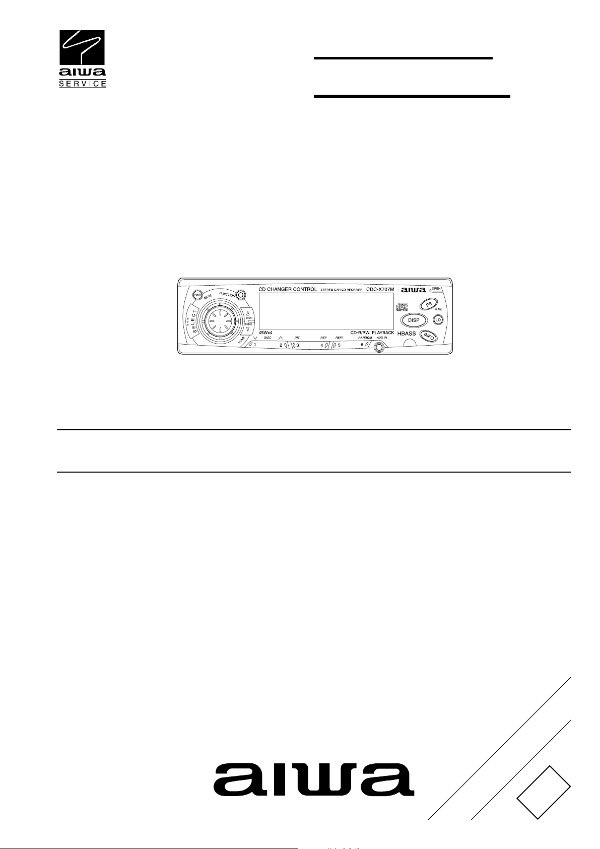
CDC-X707M
YU
CDC-X7070M
YL
SERVICE MANUAL
STEREO CAR CD RECEIVER BASIC CD MECHANISM : CDC02AW1
• This Service Manual is the "Revision Publishing" and replaces "Simple Manual"
CDC-X707M/X7070M (YU, YL), (S/M Code No. 09-002-424-3T1).
S/M Code No. 09-003-424-3R1
REVISION
DATA
Page 2

SPECIFICATIONS
RADIO SECTION
(FM)
Frequency Range 87.5 MHz –108 MHz (100 kHz steps)*
87.5 MHz –108 MHz (50 kHz steps)*
Usable Sensitivity 12.7 dBf
50 dB Quieting Sensitivity 17.2 dBf
IF Rejection 80 dB
Frequency Response 30 Hz – 15,000 Hz
S/N Ratio 63 dB
Stereo Separation 35 dB at 1 kHz
Alternate Channel Selectivity
70 dB
Capture Ratio 3 dB
(AM)
Frequency Range 530 kHz – 1,710 kHz (10 kHz steps)*
531 kHz – 1,620 kHz (9 kHz steps)*
Usable Sensitivity 30 µV (30 dB)
* Set the frequency increment for your area using the switch on the
bottom of the unit.
(The switch is set at the factory to the 10k position [for the
U.S.A.])
CD SECTION
Frequency Response 17 Hz – 20 kHz +0/–3 dB
Dynamic Range More than 80 dB
Channel Separation More than 65 dB
S/N Ratio More than 85 dB
Wow/Flutter Unmeasurable
AUDIO SECTION
Max. Power Output 45 W x 4 channels
TAPE IN input
Input Sensitivity (load impedance)
AUX IN 300 mV (10 kΩ)
GENERAL
Power Supply Voltage 14.4 V (11 to 16 V allowable),
Load Impedance 4 Ω
Tone Control Bass ±10 dB at 100 Hz
Preamp Output Voltage (load impedance)
Installation Size 182 (W) x 53 (H) x 155 (D) mm
DC, negative ground
Treble ±10 dB at 10 kHz
2.2 V (10 kΩ)
1
(7
/4 (W) x 21/8 (H) x 61/8 (D) inches)
STEERING-WHEEL-MOUNTED REMOTE CONTROL UNIT
Dimensions Approx. 67 (W) x 26 (H) x 27 (D) mm
Weight Approx. 38 g (1.33 oz.)
• Design and specifications are subject to change without
notice.
(23/4 (W) x 11/16 (H) x 11/8 (D) inches)
(excluding folder)
(including holder, battery)
– 2 –
Page 3
PROTECTION OF EYES FROM LASER BEAM DURING SERVICING
This set employs laser. Therefore, be sure to follow carefully the
instructions below when servicing.
WARNING!!
WHEN SERVICING, DO NOT APPROACH THE LASER
EXIT WITH THE EYE TOO CLOSELY. IN CASE IT IS
NECESSARY TO CONFIRM LASER BEAM EMISSION.
BE SURE TO OBSERVE FROM A DISTANCE OF MORE
THAN 30cm FROM THE SURFACE OF THE OBJECTIVE
LENS ON THE OPTICAL PICK-UP BLOCK.
Caution: Invisible laser radiation when
open and interlocks defeated avoid
exposure to beam.
Advarsel: Usynlig laserståling ved åbning,
når sikkerhedsafbrydere er ude af funktion.
Undgå udsættelse for stråling.
VAROITUS!
Laiteen Käyttäminen muulla kuin tässä käyttöohjeessa
mainitulla tavalla saataa altistaa käyt-täjän
turvallisuusluokan 1 ylittävälle näkymättömälle
lasersäteilylle.
VARNING!
Om apparaten används på annat sätt än vad som
specificeras i denna bruksanvising, kan användaren
utsättas för osynling laserstrålning, som överskrider
gränsen för laserklass 1.
CAUTION
Use of controls or adjustments or performance of procedures other than those specified herin may result in
hazardous radiation exposure.
ATTENTION
L’utillisation de commandes, réglages ou procédures
autres que ceux spécifiés peut entraîner une dangereuse
exposition aux radiations.
ADVARSEL
Usynlig laserståling ved åbning, når sikkerhedsafbrydereer
ude af funktion. Undgå udsættelse for stråling.
This Compact Disc player is classified as a CLASS 1
LASER product.
The CLASS 1 LASER PRODUCT label is located on the
rear exterior.
CLASS 1 LASER PRODUCT
KLASSE 1 LASER PRODUKT
LUOKAN 1 LASER LAITE
KLASS 1 LASER APPARAT
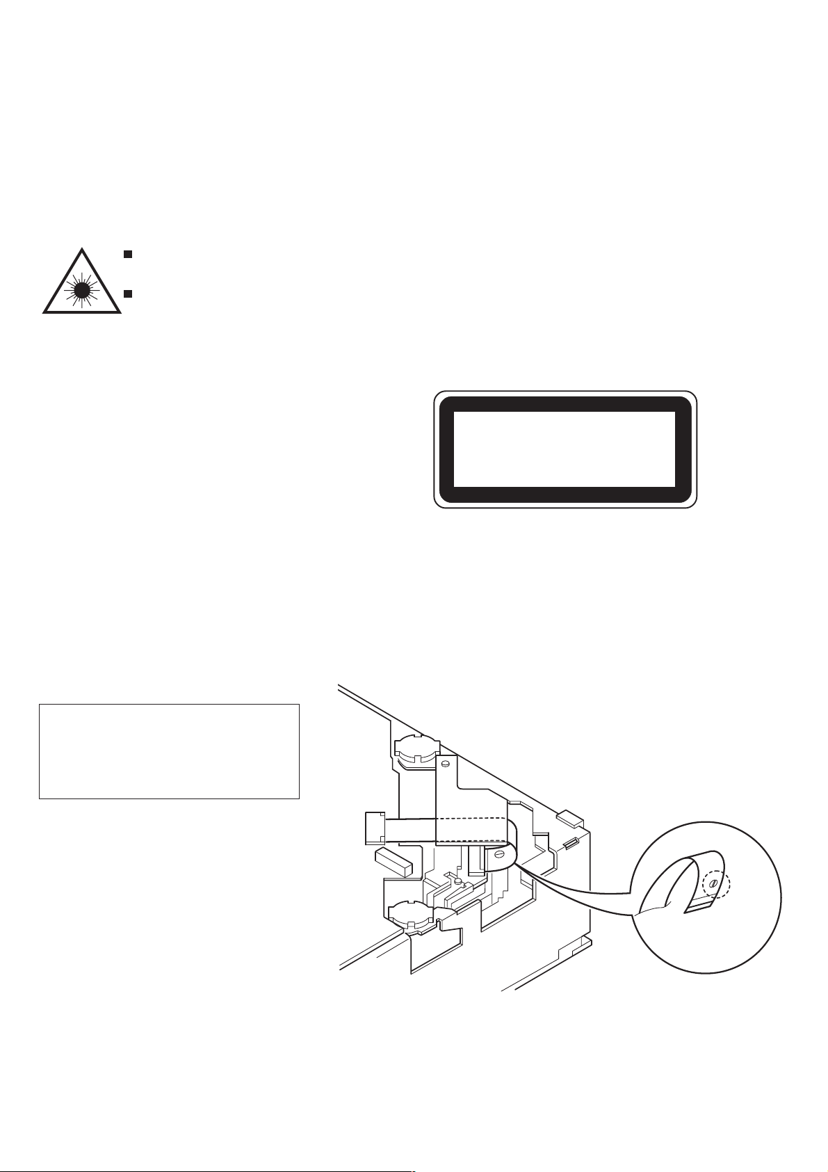
Precaution to replace Optical block
(KSS – 710A)
Body or clothes electrostatic potential could
ruin laser diode in the optical block. Be sure
ground body and workbench, and use care
the clothes do not touch the diode.
1) After the connection, remove solder
shown in right figure.
Solder
– 3 –
Page 4
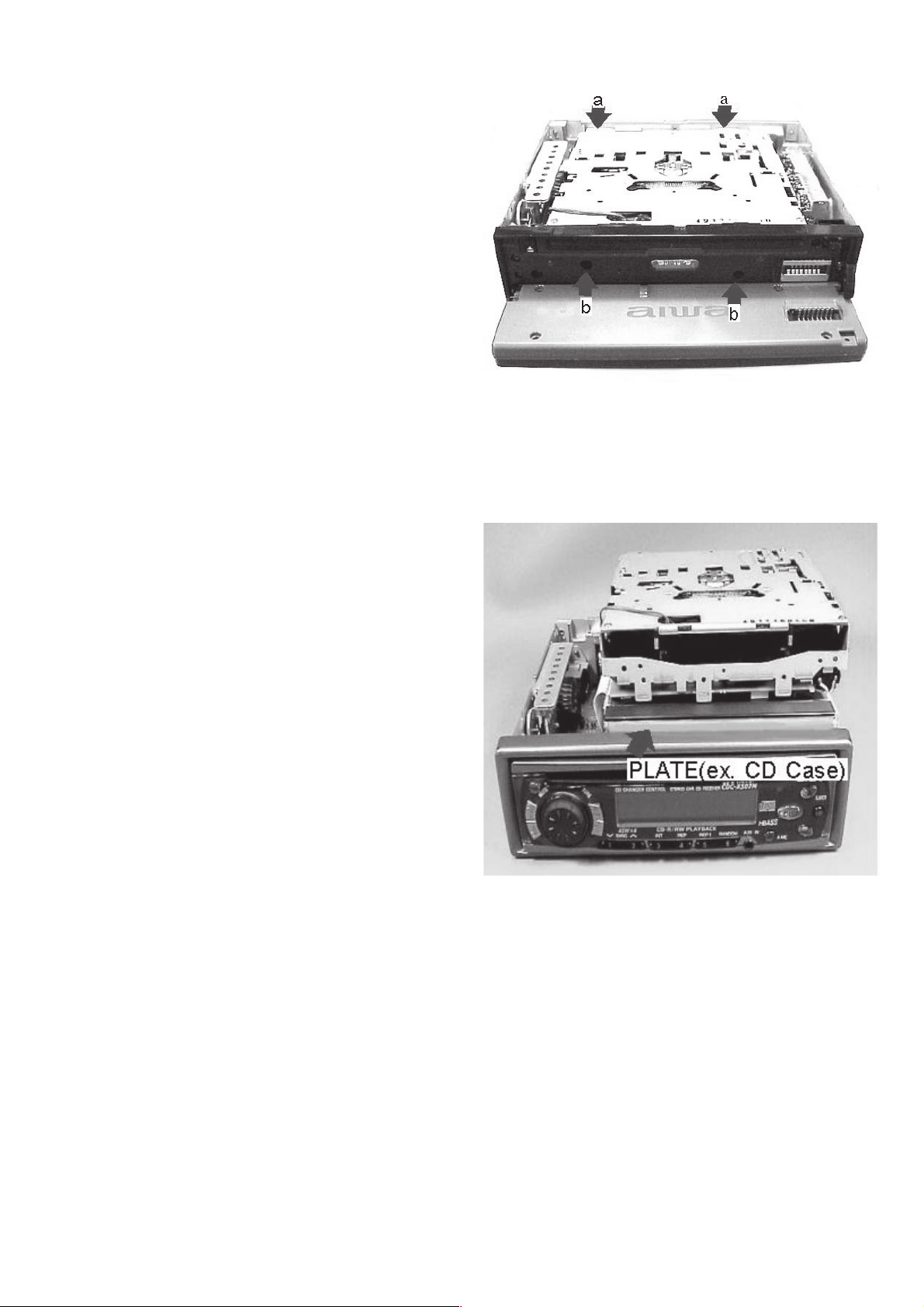
CAUTION WHEN SERVICING
1. Disassembly Instruction
1) Remove the COVER TOP / COVER BOTTOM.
2) Remove DFP.
3) Remove the four screws (indicated by arrows) from CD
mechanism.
Screw (a) × 2: VTT 2.6-6
Screw (b) × 2: VTT 2.6-3B
(Fig. 1)
Fig. 1
2. Servicing Position
Check operations in stable position.
Example: Use PLATE or the like.
(Fig. 2)
Fig. 2
– 4 –
Page 5

ELECTRICAL MAIN PARTS LIST
PART NO. DESCRIPTIONREF. NO. KANRI
NO.
IC
8Z-KT1-622-010 C-IC,LC75374E
87-A21-562-010 IC,LA4743B
88-KT1-608-010 C-IC,LC75854W
87-A90-951-010 RCR UNIT,SBX1971-52
87-A21-622-030 C-IC,UPD178006AGC-540-3B9<YL>
87-A21-623-030 C-IC,UPD178016AGC-562-3B9<YU>
88-KT1-606-080 IC,PST994D
87-020-784-080 IC,TC4053BF
87-A21-467-010 C-IC,CXA2581N
87-A21-533-030 C-IC,CXD2587Q
87-017-888-080 IC,NJM4558MD
87-A21-534-030 C-IC,UPD78012FGC656-AB8
87-A21-161-040 C-IC,BA6392FP
87-A20-712-040 C-IC,BA6417F
TRANSISTOR
87-026-235-080 CHIP-TR,DTC114EK
87-A30-289-040 C-TR,2SA1037AK(R)
89-324-122-080 C-TR,2SC2412KR
87-A30-218-080 TR,2SB1237(Q)<YL>
87-A30-287-040 C-TR,DTC114TKA
87-A30-300-080 TR,2SB1277
87-A30-299-080 TR,2SB1326
87-A30-302-040 C-TR,2SD1758-F5
87-A30-298-080 TR,2SD2396
89-211-323-080 C-TR,2SB1132R
87-A30-279-040 C-TR,DTC314TK
89-423-953-010 TR,2SD2395F
87-A30-248-040 C-TR,2SB1197KQ
87-A30-011-080 C-TR,DTB113ZK
87-A30-273-040 C-TR,DTC124EKA
87-026-210-040 C-TR,DTC144EK
DIODE
87-A40-250-080 C-DIODE,DAN217
87-001-783-080 DIODE,1N4002
87-070-136-080 ZENER,MTZJ5.1B
87-A40-798-010 DIODE,1N5402 (3A/200V)
87-A40-523-080 ZENER,MTZJ9.1B
87-070-334-080 ZENER,MTZJ10B
87-A40-509-080 ZENER,MTZJ6.8C
87-A40-189-080 DIODE,1SR139-400
87-020-465-080 DIODE,1SS133 (110MA)
87-A40-624-080 ZENER,MTZJ10A
87-020-585-080 CHIP-ZENER,02CZ6.2Y
87-A40-620-080 ZENER,MTZJ6.2A
87-017-932-080 ZENER,MTJ6.2B
87-A40-650-080 ZENER,MTZJ6.8A
87-020-331-080 C-DIODE,DAN202K
MAIN C.B.
C102 87-010-197-080 CAP, CHIP 0.01-25
C103 87-010-322-080 C-CAP,S 100P-50 CH
C104 87-010-498-040 CAP,E 10-16 GAS
C105 87-010-498-040 CAP,E 10-16 GAS
C106 87-010-322-080 C-CAP,S 100P-50 CH
C107 87-010-322-080 C-CAP,S 100P-50 CH
C108 87-010-805-080 CAP, S 1-16
C109 87-010-805-080 CAP, S 1-16
C110 87-010-186-080 CAP,CHIP 4700P-50
C111 87-010-196-080 CHIP CAPACITOR,0.1-25
C112 87-010-197-080 CAP, CHIP 0.01-25
C113 87-010-495-040 CAP,E 2.2-50 GAS
C119 87-010-196-080 CHIP CAPACITOR,0.1-25
C121 87-010-220-080 C-CAP,S 0.018-25 B<YL>
C121 87-012-365-080 C-CAP,S 0.027-25VBK<YU>
DESCRIPTIONREF. NO. KANRI
PART NO.
NO.
C122 87-010-220-080 C-CAP,S 0.018-25 B<YL>
C122 87-012-365-080 C-CAP,S 0.027-25VBK<YU>
C123 87-010-178-080 CHIP CAP 1000P-50
C125 87-010-197-080 CAP, CHIP 0.01-25
C126 87-010-197-080 CAP, CHIP 0.01-25
C128 87-010-197-080 CAP, CHIP 0.01-25
C210 87-016-669-080 C-CAP,S 0.1-25 K B
C211 87-010-182-080 C-CAP,S 2200P-50 B
C212 87-015-629-080 CHIP CAPACITOR, 0.0022
C251 87-012-368-080 C-CAP,S 0.1-50 K B
C252 87-010-182-080 C-CAP,S 2200P-50 B
C253 87-018-119-080 CAP, TC U100P-50V
C254 87-010-322-080 C-CAP,S 100P-50 CH
C255 87-018-119-080 CAP, TC U100P-50V
C256 87-018-119-080 CAP, TC U100P-50V
C257 87-018-119-080 CAP, TC U100P-50V
C258 87-010-297-080 C-CAP,S 100P-50 CH
C259 87-018-119-080 CAP, TC U100P-50V
C260 87-018-119-080 CAP, TC U100P-50V
C261 87-018-205-080 CAP, TC U 0.022-25
C264 87-010-553-040 CAP,E 47-16 GAS
C265 87-010-498-040 CAP,E 10-16 GAS
C266 87-010-194-080 CAP, CHIP 0.047-25
C268 87-010-498-040 CAP,E 10-16 GAS
C269 87-010-555-040 CAP,E 100-10 GAS
C270 87-010-555-040 CAP,E 100-10 GAS
C280 87-015-629-080 CHIP CAPACITOR, 0.0022-50
C281 87-012-368-080 C-CAP,S 0.1-50 F<YL>
C282 87-012-368-080 C-CAP,S 0.1-50 F<YL>
C283 87-012-368-080 C-CAP,S 0.1-50 F<YL>
C284 87-012-368-080 C-CAP,S 0.1-50 F<YL>
C401 87-010-805-080 C-CAP,S 1-16<YU>
C402 87-010-805-080 C-CAP,S 1-16<YU>
C403 87-010-805-080 CAP, S 1-16
C404 87-010-805-080 CAP, S 1-16
C407 87-010-805-080 CAP, S 1-16
C408 87-010-805-080 CAP, S 1-16
C409 87-010-498-040 CAP,E 10-16 M 5L SRE
C410 87-010-498-040 CAP,E 10-16 M 5L SRE
C411 87-010-805-080 CAP, S 1-16
C412 87-010-805-080 CAP, S 1-16
C413 87-010-498-040 CAP,E 10-16 M 5L SRE
C414 87-010-498-040 CAP,E 10-16 M 5L SRE
C415 87-010-498-040 CAP,E 10-16 M 5L SRE
C416 87-010-498-040 CAP,E 10-16 M 5L SRE
C417 87-010-498-040 CAP,E 10-16 M 5L SRE
C418 87-010-498-040 CAP,E 10-16 M 5L SRE
C419 87-010-498-040 CAP,E 10-16 M 5L SRE
C420 87-010-555-040 CAP,E 100-10 GAS
C421 87-010-805-080 CAP, S 1-16
C422 87-010-805-080 CAP, S 1-16
C423 87-010-805-080 CAP, S 1-16
C424 87-010-805-080 CAP, S 1-16
C425 87-012-140-080 CAP 470P-50
C426 87-012-140-080 CAP 470P-50
C427 87-012-140-080 CAP 470P-50
C428 87-012-140-080 CAP 470P-50
C429 87-010-498-040 CAP,E 10-16 M 5L SRE
C430 87-010-498-040 CAP,E 10-16 GAS
C431 87-010-184-080 CHIP CAPACITOR 3300P-50
C432 87-010-184-080 CHIP CAPACITOR 3300P-50
C433 87-010-198-080 CAP, CHIP 0.022-25
C434 87-010-198-080 CAP, CHIP 0.022-25
C435 87-A11-177-080 C-CAP,S 0.15-16 K B
C436 87-A11-177-080 C-CAP,S 0.15-16 K B
C437 87-A11-177-080 C-CAP,S 0.15-16 K B
C438 87-A11-177-080 C-CAP,S 0.15-16 K B
C439 87-010-196-080 CHIP CAPACITOR,0.1-25
C440 87-012-141-080 CHIP-CAPACITOR,0.22-16F
C441 87-012-141-080 CHIP-CAPACITOR,0.22-16F
– 5 –
Page 6

PART NO. DESCRIPTIONREF. NO. KANRI
C461 87-010-450-080 CAPACITOR 0.47-16
C462 87-012-358-080 C-CAP,S 0.47-10 F Z
C463 87-012-358-080 C-CAP,S 0.47-10 F Z
C464 87-010-196-080 CHIP CAPACITOR,0.1-25
C501 87-016-669-080 C-CAP,S 0.1-25 K B
C502 87-010-182-080 C-CAP,S 2200P-50 B
C551 87-010-805-080 CAP, S 1-16
C552 87-010-805-080 CAP, S 1-16
C553 87-010-805-080 CAP, S 1-16
C554 87-010-805-080 CAP, S 1-16
C555 87-010-178-080 CHIP CAP 1000P
C556 87-010-178-080 CHIP CAP 1000P
C557 87-010-178-080 CHIP CAP 1000P
C558 87-010-178-080 CHIP CAP 1000P
C559 87-010-498-040 CAP,E 10-16 GAS
C560 8A-KC7-623-000 CAP,E 2200U-16 BT(125C)
C561 87-010-805-080 CAP, S 1-16
C563 87-010-497-040 CAP,E 4.7-35 GAS
C901 87-010-198-080 CAP, CHIP 0.022-25
C902 87-010-198-080 CAP, CHIP 0.022-25
C903 87-010-194-080 CAP, CHIP 0.047-25
C904 87-010-198-080 CAP, CHIP 0.022-25
C905 87-010-498-040 CAP,E 10-16 GAS
C906 87-010-553-040 CAP,E 47-16 GAS
C907 87-010-497-040 CAP,E 4.7-35 GAS
C908 87-010-196-080 CHIP CAPACITOR,0.1-25
C909 87-010-315-080 C-CAP,S 27P-50 CH
C910 87-016-039-010 CAP,DL 0.022F-5.5 Z 70
C911 87-010-315-080 C-CAP,S 27P-50 CH
C912 87-010-196-080 CHIP CAPACITOR,0.1-25
C913 87-010-198-080 CAP, CHIP 0.022-25
C914 87-010-198-080 CAP, CHIP 0.022-25
C915 87-012-350-080 C-CAP,1-25 F
C916 87-018-119-080 CAP, TC U100P-50V
C917 87-018-119-080 CAP, TC U100P-50V
C919 87-010-498-040 CAP,E 10-16 GAS
C920 87-010-198-080 CAP, CHIP 0.022-25
C923 87-010-178-080 CHIP CAP 1000P-50
C924 87-010-196-080 CHIP CAPACITOR,0.1-25
C927 87-010-805-080 CHIP CAPACITOR,1-16
C928 87-015-627-080 C-CAP,1000P-50 B
CNA101 8A-KC8-614-010 CONN ASSY,2P SHLD
CON201 8Z-KT1-611-010 CONN,16P CAM-B51
CON901 87-A61-219-010 CONN,20P H 52089-2020
CON902 87-A60-182-010 CONN,16P TKC-F16P-E3
D909 87-027-262-010 LEDE,TLR-124(RED)
F281 8Z-KC1-621-010 FUSE,15A 32V
!
FC901 88-KC4-641-010 FF-CABLE,20P 1.0 90MM
J101 8Z-KT1-614-010 ANT,AW-002
J451 87-A61-224-010 JACK,PIN 4P XR-401
J951 8A-KC7-620-010 JACK,DIN 13 P SKDS1302
L101 87-003-143-080 COIL 4.7 UH
L104 8Z-KT1-619-010 COIL,68MH K7-D
L201 8Z-KT1-615-010 FLTR,AMORPHOUS -CHOKE
L252 87-003-149-080 COIL,47UH
L401 87-003-143-080 COIL 4.7 UH
L901 87-003-147-080 COIL, 22UH
L903 87-003-149-080 COIL,47UH
L904 87-003-102-080 COIL, 10UH
L905 87-003-102-080 COIL, 10UH
L906 87-003-102-080 COIL, 10UH
PL901 8Z-KT1-641-010 LAMP,T-3
SW901 87-A91-070-010 SW,TACT SKHHLV
SW903 87-036-109-010 SW MICRO SPPB61
SW904 87-A91-152-010 SW,SL 1-1-2 SSSS212-11-A
TU101 8A-KC8-621-010 TU UNIT, FAE347-A12
X901 87-A70-175-010 VIB,XTAL 4.5MHZ AT-49
FRONT C.B.
NO.
DESCRIPTIONREF. NO. KANRI
PART NO.
NO.
C702 87-010-196-080 CHIP CAPACITOR,0.1-25
C703 87-010-805-080 CAP, S 1-16
C704 87-010-805-080 CAP, S 1-16
C705 87-010-154-080 CAP CHIP 10P-50
C706 87-010-176-080 C-CAP,S 680P-50 SL
C707 87-010-194-080 CAP, CHIP 0.047-25
C708 87-010-194-080 CAP, CHIP 0.047-25
C709 87-010-196-080 CHIP CAPACITOR,0.1-25
C710 87-010-194-080 CAP, CHIP 0.047-25
C711 87-010-194-080 CAP, CHIP 0.047-25
CON701 8Z-KT1-612-010 CONN,16P CAM-C73
D719 87-A40-813-040 C-LED,SEC1E01C BLUE
D720 87-A40-813-040 C-LED,SEC1E01C BLUE
D721 87-A40-813-040 C-LED,SEC1E01C BLUE
D725 87-017-827-070 C-LED,SEC 1201C RED
D726 87-017-827-070 C-LED,SEC 1201C RED
D727 87-017-827-070 C-LED,SEC 1201C RED
LCD701 8A-KC8-610-010 LCD,AKC-2/8(2 COLOR)
PL701 8Z-KT1-641-010 LAMP,T-3
PL702 8Z-KT1-641-010 LAMP,T-3
SW701 87-036-251-080 SW,TACT SKQCAE
SW702 87-036-251-080 SW,TACT SKQCAE
SW703 87-A90-001-080 C-SW,TACT SKQMAL
SW704 87-036-251-080 SW,TACT SKQCAE
SW705 87-036-251-080 SW,TACT SKQCAE
SW706 87-036-251-080 SW,TACT SKQCAE
SW707 87-036-251-080 SW,TACT SKQCAE
SW708 87-A90-001-080 C-SW,TACT SKQMAL
SW709 87-036-251-080 SW,TACT SKQCAE
SW710 87-036-251-080 SW,TACT SKQCAE
SW711 87-A90-001-080 C-SW,TACT SKQMAL
SW712 87-036-251-080 SW,TACT SKQCAE
SW713 87-036-251-080 SW,TACT SKQCAE
SW714 87-036-251-080 SW,TACT SKQCAE
SW715 87-A90-001-080 C-SW,TACT SKQMAL
SW716 87-A91-597-010 SW,RTRY SIM-026MT
CONN C.B.
CON601 8Z-KT1-613-010 CONN,16P CAM-C74
CON602 87-A60-910-010 C-CONN,16P V TKC-F16X-H2
EJECT C.B.
CNA601 8A-KC8-613-010 CONN ASSY,3P EJECT
D950 87-A40-641-010 LED,SLR-332MG GRN
SW950 87-A90-001-080 C-SW,TACT SKQMAL
AUX C.B.
FC751 8A-KC7-611-010 F-CABLE,3P (AUX)
J751 85-HRL-623-010 JACK,3.5 ST BLK
CD MAIN C.B
C803 87-A10-711-080 C-CAP,E 100-6.3 M MF
C804 87-010-178-080 CHIP CAP 1000P
C805 87-016-669-080 C-CAP,S 0.1-25 K B
C806 87-010-184-080 CHIP CAPACITOR 3300P(K)
C808 87-016-669-080 C-CAP,S 0.1-25 K B
C809 87-010-880-080 C-CAP,E 47-6.3 MF
C811 87-016-669-080 C-CAP,S 0.1-25 K B
C813 87-016-669-080 C-CAP,S 0.1-25 K B
C816 87-010-880-080 C-CAP,E 47-6.3 MF
C831 87-012-156-080 C-CAP,S 220P-50 CH
C832 87-010-194-080 CAP, CHIP 0.047
C833 87-012-156-080 C-CAP,S 220P-50 CH
C834 87-012-156-080 C-CAP,S 220P-50 CH
C835 87-016-669-080 C-CAP,S 0.1-25 K B
C836 87-012-156-080 C-CAP,S 220P-50 CH
– 6 –
Page 7

PART NO. DESCRIPTIONREF. NO. KANRI
NO.
C837 87-010-186-080 CHIP CAPACITOR 4700P(K)
C838 87-010-194-080 CAP, CHIP 0.047
C839 87-010-880-080 C-CAP,E 47-6.3 MF
C840 87-016-669-080 C-CAP,S 0.1-25 K B
C841 87-016-669-080 C-CAP,S 0.1-25 K B
C842 87-016-526-080 C-CAP,S 0.47-16 BK
C843 87-012-155-080 C-CAP 180P-50CH
C844 87-012-155-080 C-CAP 180P-50CH
C845 87-010-177-080 C-CAP,S 820P-50 SL
C846 87-010-177-080 C-CAP,S 820P-50 SL
C847 87-010-885-080 C-CAP,E 22-10 MF
C848 87-010-885-080 C-CAP,E 22-10 MF
C849 87-010-318-080 C-CAP,S 47P-50 CH
C850 87-010-318-080 C-CAP,S 47P-50 CH
C851 87-A12-034-080 C-CAP,E 2.2-35 M MF
C852 87-A12-034-080 C-CAP,E 2.2-35 M MF
C853 87-010-178-080 CHIP CAP 1000P
C854 87-010-178-080 CHIP CAP 1000P
C855 87-A10-473-080 C-CAP,E 47-10 MF10FC(M)
C856 87-016-669-080 C-CAP,S 0.1-25 K B
C857 87-010-880-080 C-CAP,E 47-6.3 MF
C861 87-016-669-080 C-CAP,S 0.1-25 K B
C862 87-016-669-080 C-CAP,S 0.1-25 K B
C863 87-010-880-080 C-CAP,E 47-6.3 MF
C881 87-A10-473-080 C-CAP,E 47-10 MF10FC(M)
C882 87-016-669-080 C-CAP,S 0.1-25 K B
C883 87-016-669-080 C-CAP,S 0.1-25 K B
C884 87-010-178-080 CHIP CAP 1000P
C885 87-A10-473-080 C-CAP,E 47-10 MF10FC(M)
C886 87-016-669-080 C-CAP,S 0.1-25 K B
DESCRIPTIONREF. NO. KANRI
PART NO.
NO.
C887 87-016-669-080 C-CAP,S 0.1-25 K B
C888 87-016-669-080 C-CAP,S 0.1-25 K B
C889 87-A10-473-080 C-CAP,E 47-10 MF10FC(M)
C891 87-012-156-080 C-CAP,S 220P-50 CH
C892 87-012-156-080 C-CAP,S 220P-50 CH
C893 87-012-156-080 C-CAP,S 220P-50 CH
C894 87-012-156-080 C-CAP,S 220P-50 CH
C895 87-012-156-080 C-CAP,S 220P-50 CH
C896 87-012-156-080 C-CAP,S 220P-50 CH
C897 87-012-156-080 C-CAP,S 220P-50 CH
CN801 87-A61-125-080 C-CONN,16P H FLZ-SM1-TB
CN891 87-A61-220-080 C-CONN,20P H 52271-2090
L801 87-A50-536-080 C-COIL,10UH K LQH3C24
L802 87-A50-536-080 C-COIL,10UH K LQH3C24
L831 87-A50-536-080 C-COIL,10UH K LQH3C24
L832 87-A50-536-080 C-COIL,10UH K LQH3C24
L833 87-A50-536-080 C-COIL,10UH K LQH3C24
L861 87-A50-536-080 C-COIL,10UH K LQH3C24
L881 87-A50-536-080 C-COIL,10UH K LQH3C24
S861 87-A91-627-080 SW,PUSH MPU10372MLBO
X831 87-A70-262-080 C-VIB,16.93MHZ CSTCW
X861 87-A70-251-080 C-VIB,CER 10.00MHZ CSTCC
SENSOR C.B
SW1 87-A91-627-080 SWITCH
SW2 87-A91-627-080 SWITCH
– 7 –
Page 8
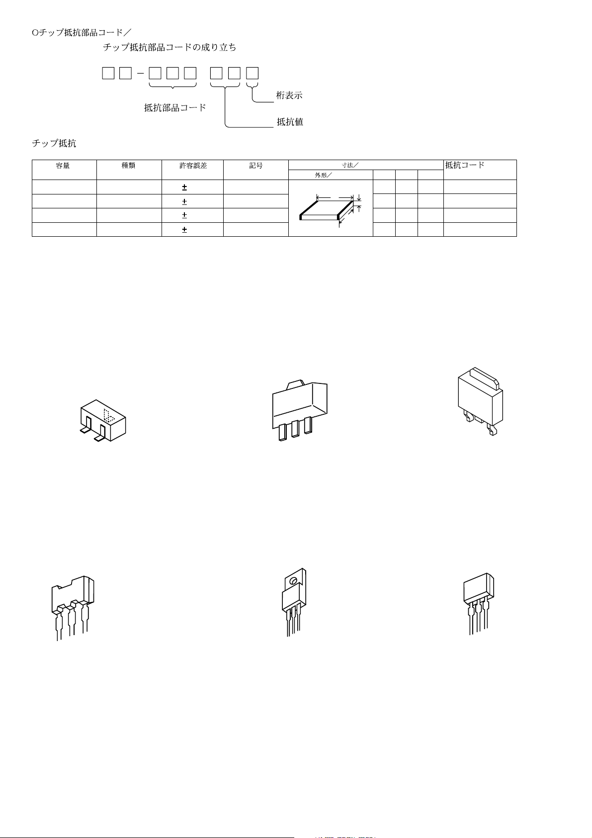
CHIP RESISTOR PART CODE
Chip Resistor Part Coding
88
A
Resistor Code
Chip resistor
Wattage Type Tolerance
1/16W 1005 5% CJ
1/16W
1/10W
1/8W
1608
2125
3216
5%
5%
5%
TRANSISTOR ILLUSTRATION
Symbol
CJ
CJ
CJ
Figure
Value of resistor
Form
L
C
Dimensions (mm)
t
W
0.55
Resistor Code
108
118
128
LW t
1.0 0.5 0.35 104
1.6 0.8 0.45
2 1.25 0.45
3.2
1.6
: A
: A
C
B
E
2SA1037
2SC2412
DTC114EK
DTC114TKA
DTC314TK
E C B
2SB1237
C
2SB1197KQ
DTB113ZK
DTC124EKA
DTC144EK
B
2SB1132
B C E
2SD2395
2SD2396
B
E
E
2SD1758
E C B
2SB1277
2SB1326
– 8 –
Page 9
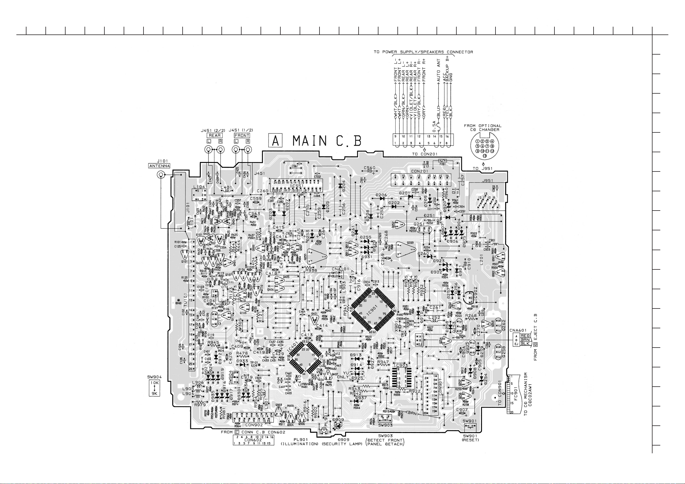
WIRING – 1 (MAIN)
101112131415161718192021222324
1234567892526272829303132
A
B
C
D
E
F
G
H
I
J
K
L
M
N
O
P
Q
– 9 –
R
S
T
U
Page 10
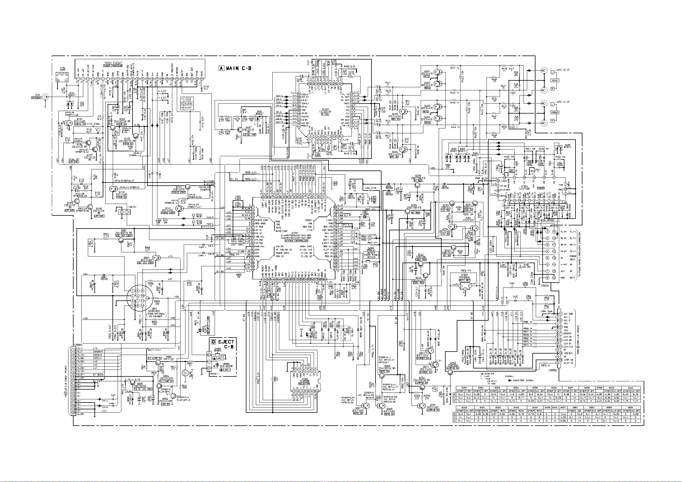
SCHEMATIC DIAGRAM – 1 (MAIN / EJECT)
– 10 –
Page 11
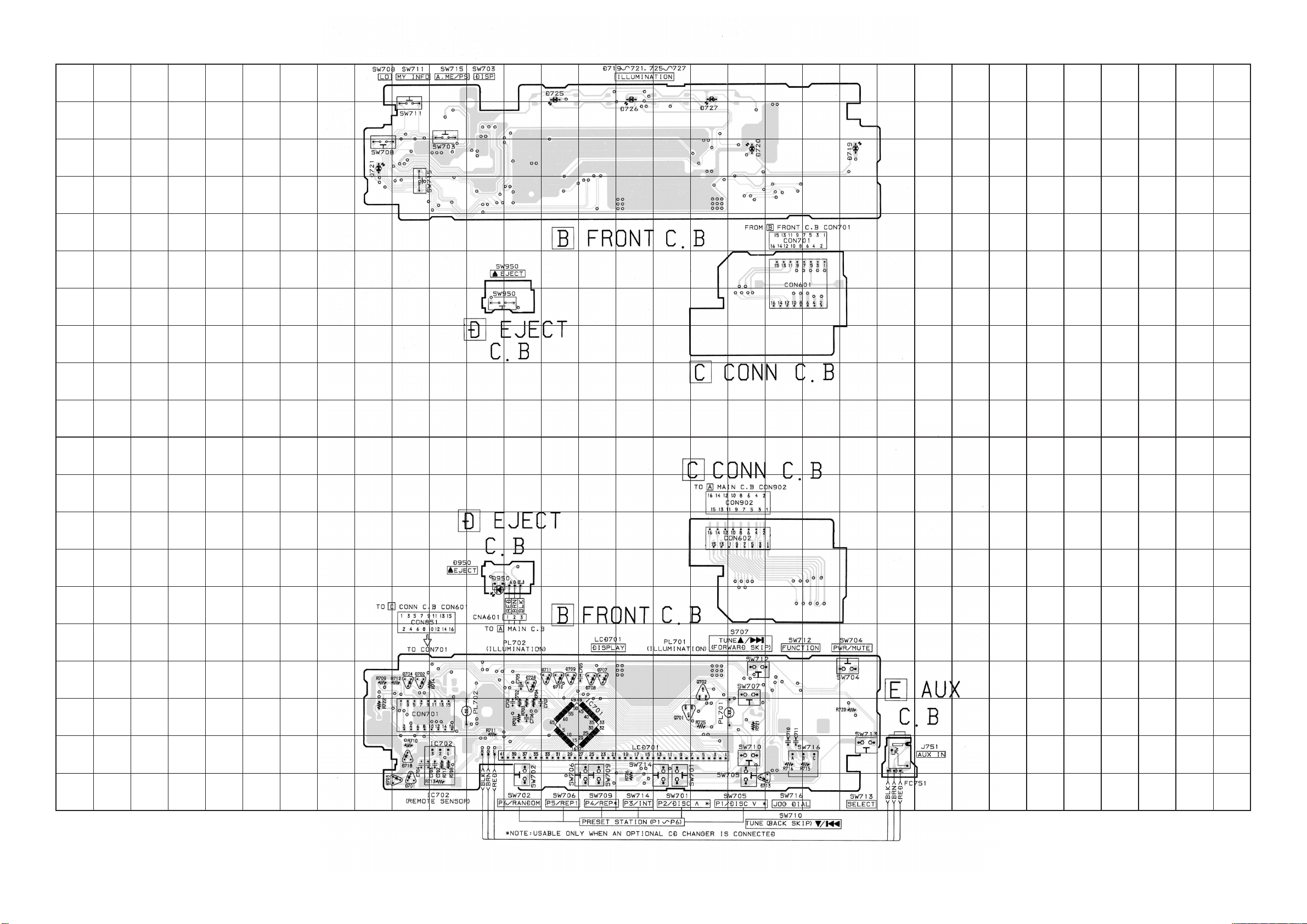
WIRING – 2 (FRONT / CONN / AUX / EJECT)
J
I
H
G
F
E
D
C
B
A
2223242526272829303132
2223242526272829303132
161718192021
161718192021
123456789101112131415
123456789101112131415
A
B
C
D
E
F
G
– 11 –
H
I
J
Page 12

SCHEMATIC DIAGRAM – 2 (FRONT / CONN / AUX)
– 12 –
Page 13

WIRING – 3 (CD MAIN / SENSOR) <1 / 2>
181920212223242526272829303132
17 16 15 14 13 12 11 10 9 8 7 6 5 4 3 2 1
A
B
C
D
E
F
G
H
I
J
K
L
M
N
O
P
Q
– 13 –
R
S
T
U
Page 14

WIRING – 3 (CD MAIN) <2 / 2>
A
B
C
D
E
F
G
H
151413121110987654321
16 17 18 19 20 21 22 23 24 25 26 27 28 29 30 31 32
I
J
K
L
M
N
O
P
Q
R
S
T
U
– 14 –
Page 15

SCHEMATIC DIAGRAM – 3 (CD MAIN / SENSOR)
– 15 –
Page 16

LCD DISPLAY
LCD,AKC-2/8(2 COLOR)
– 16 –
Page 17

IC DESCRIPTION
IC, µPD178016AGC-562-3B9/µPD178006AGC-540-3B9
Pin No. Pin Name I/O Description
1
FM/AM S-M
I
RDS AF signal input and FM/AM S meter signal input.
10
11
12
13
14
15
16
17
18
19
20
21
22
23
24
25
26
27
28
29
30
31
32
33
34
35
36
37
2
3
4
5
6
7
8
9
LEVEL-M
A-VOL CONT
CD CONNECT
CD DISP SEL
CD CLO
CD DI
CD DO
CD CLI
LCD CE
CLK SEL
CDS DI/LCD DI
CDS DO/LCD DO
CDS CLO/LCD CLO
CD ACC CONT
POWER MUTE
ST-BY MUTE
POWER CONT
CONT 1
CONT 2
GND
VDD
MUTE
BAND CONT
RADIO CONT
RDS MODE
IF REQ
AM IF
FM IF
VDD PLL
FM OSC
AM OSC
GND PLL
EO 0
EO 1
GND
LOC/DX
I
Voltage input for level indicator. Pulled down when not used.
I
Detects microphone input for auto volume operation. Pulled down when not used.
I
CD changer connection check. Pulled down when not used.
O
Output communication timing signal output to CD changer. (Hi=TX, Low=RX).
O
Synchronous clock signal output to CD changer.
I
Data input from CD changer. Pulled down when not used.
O
Data output to CD changer.
I
Synchronous clock signal input from CD changer. Pull down when not used.
O
LCD DRV (LC75854W) CE output.
O
Clock selection for CDS and LCD DRV (LC75854W). (Hi=CDS, Low=LCD).
I
CDS and LCD DRV (LC75854W) data input.
O
CDS and LCD DRV (LC75854W) data output.
O
CDS and LCD DRV (LC75854W) synchronous clock output.
O
CD changer ACC signal output.
O
Muting output to power amp.
O
Standby/muting output to power amp.
O
Unit power control output.
O
LCD contrast control 1.
O
LCD contrast control 2.
–
Ground for port.
–
Power supply for port.
O
Audio muting output.
O
AM/FM power switching output. (Hi =AM, Low=FM).
O
Radio power switching output. (Low=radio mode).
O
Hi output during RDS AF operation.
O
Output to request IF count signal.
I
AM IF count signal input.
I
FM IF count signal input.
–
Power supply for PLL.
I
FM local oscillation input.
I
AM local oscillation input.
–
Ground for PLL.
O
Error output from charge pump.
O
Error output from charge pump.
–
Ground.
O
LOC/DX switching output during radio seek.(Hi=LOC, Low=DX).
38
39
40
ST IND/SD IN
PHONE MUTE
CDS CS
I
I
CS signal output.
O
Stereo signal input during FM reception. (Hi=MONO, Low=ST) /Broadcast detection
signal input during FM/AM seek. (Hi=detect broadcast).
Mute control from external. Low=20dB MUTE. Pull up when not used.
– 17 –
Page 18

Pin No. Pin Name I/O Description
41
42
43
44
45
46
47
48
49
50
51
52
53
54
55
56
57
58
59
60
61
62
63
64
65
66
67
68
69
70
71
72
73
74
75
76
77
78
79
80
CDS RESET
CDS SLEEP
CDS STOP
CDS IN
TEST MODE
NC
NC
LED
MI-1
MI-2
MI-3
MO-1
MO-2
MO-3
MO-4
NC
NC
ACC IN
BEEP
RMT IN
E-VOL CE
E-VOL DO
E-VOL CLO
DSSA CONT
RDS DI
DFP IN
FLAP IN
RDS CLI
EJECT IN
BATT IN
RE1 IN
RE2 IN
CDS SREQ
REG CPU
GND
X-OUT
X-IN
REG OSC
VDD
RESET
O
Reset signal output.
O
SLEEP signal output.
I
STOP signal input.
I
DISC status detection input.
I
CD test port.
_
Not connected (open).
_
Not connected (open).
O
Security LED flashing output. (Hi=120~130ms, 1cycle=3sec).
Diode matrix input for initial setting.
I
Diode matrix output for initial setting.
O
–
Not connected (open).
–
Not connected (open).
I
ACC (power supply for accessories) ON/OFF input .
O
Beep output (3 kHz, 50 ms).
I
Remote controller input. Pulled up when not used.
O
CE output to electronic VR (LC75374E).
O
Data output to electronic VR (LC75374E).
O
Clock output to electronic VR (LC75374E).
O
Output Hi during DSSA L/R operation.
I
RDS data input. Pulled down when not used.
I
Detect front panel existance.
I
Detect whether flap DFP is open or closed. DFP IN = enable when Hi.
I
RDS clock input. Pulled down when not used.
I
Eject detection input. FLAP IN = enable when Low. Pulled up when not used.
I
Battery ON/OFF input.
I
Rotary encoder input 1.
I
Rotary encoder input 2.
I
CDS S-REQ signal input.
I
CPU power regulator.
–
Ground.
–
System clock oscillator.
–
System clock oscillator.
–
Regulator for oscillator circuit.
–
Power supply.
–
System reset input.
– 18 –
Page 19

IC, LC75854W
Pin No. Pin Name I/O Description
1 ~ 39
40
41
42
43
44
45
46 ~ 49
50 ~ 54
55
56
57, 58
59
60
61
62
63
S1~S39
COM1
COM2
COM3
COM4
KS1
KS2
KS3 ~ KS6
KI1 ~ KI5
TEST
VDD
VDD1, VDD2
VSS
OSC
DO
CE
CL
O
O
O
O
O
–
–
O
–
–
–
–
O
I/O
LCD segments output.
LCD common driver outputs.
LCD common driver outputs.
LCD common driver outputs.
LCD common driver outputs.
Not used.
Not used.
Key scan outputs.
I
Key scan inputs.
Test pin (Connected to GND).
5V.
VDD.
GND.
I
Oscillator.
Communication; data output.
I
Communication; chip enable.
Communication; sync clock.
64
DI
I
Communication; data transferred.
– 19 –
Page 20

IC, CXD2587Q
Pin No. Pin Name I/O Description
1
SQSO
O
Sub-Q 80-bit and PCM peak/level data output. CD TEXT data output.
10
11
12
13
14
15
16
17
18
O
—
I/O
O
O
O
O
O
I
Clock input for reading SQSO.
I
System reset. Reset at "L".
I
Muting input. Muted at "H".
I
Serial data input from CPU.
I
Latch input from CPU. Latches serial data at the trailing edge.
I
Clock input for serial data transfer from CPU.
SENS output to CPU.
I
Clock input for reading SENS serial data.
Power supply of digital circuits.
Input/output for anti-shock.
I
Microprocessor extended interface (input A).
I
Microprocessor extended interface (input B).
Microprocessor extended interface (output).
WFCK output.
WUGF output. MNT1 or RFCK is output when switched by command.
XPCK output. MNT0 is output when switched by command.
GFS output. MNT3 or XROF is output when switched by command.
2
3
4
5
6
7
8
9
SQCK
XRST
SYSM
DATA
XLAT
CLOK
SENS
SCLK
VDD
ATSK
SPOA
SPOB
XLON
WFCK
XUGF
XPCK
GFS
19
20
21
22
23
24
25
26
27
28
29
30
31
32
33
34
C2PO
SCOR
COUT
MIRR
DFCT
FOK
LOCK
MDP
SSTP
SFDR
SRDR
TFDR
TRDR
FFDR
FRDR
VSS
O
O
I/O
I/O
I/O
I/O
I/O
O
O
O
O
O
O
O
—
C2PO output. GTOP is output when switched by command.
Outputs "H" when Sub-code sync S0 or S1 is detected.
Track number count signal input/output.
Mirror signal input/output.
Defect signal input/output.
Focus OK signal input/output.
Outputs "H" when GFS sampled by 460 Hz is "H"; "L" when GFS is "L" continuously
for 8 samplings. Or, a signal is input when LKIN is "1".
Spindle motor servo control output.
I
Disc innermost edge detection signal input.
Sled drive output.
Sled drive output.
Tracking drive output.
Tracking drive output.
Focus drive output.
Focus drive output.
Ground of digital circuits.
35
36
37
38
39
TEST
TES1
XTSL
VC
FE
I
TEST pin. Normally, grounded.
I
TEST pin. Normally, grounded.
Crystal select input. "L" when 16.9344MHz crystal is used; "H" when 33.8688MHz
I
crystal is used.
I
Neutral voltage input.
I
Focus error signal input.
– 20 –
Page 21

Pin No. Pin Name I/O Description
40
41
42
43
44
45
46
47
48
49
50
51
52
53
54
55
56
SE
TE
CE
RFDC
ADIO
AVSS0
IGEN
AVDD0
ASYO
ASYI
BIAS
RFAC
AVSS3
CLTV
FILO
FILI
PCO
—
—
—
I
Sled error signal input.
I
Tracking error signal input.
I
Neutral servo analog input.
I
RF signal input.
O
For test. Do not connect.
Ground of analog circuits.
I
Constant current input for OP amp.
Power supply of analog circuits.
O
EFM full-swing output ("L": Vss; "H": VDD).
I
Asymmetry comparator voltage input.
I
Asymmetry circuit constant current input.
I
EFM signal input.
Ground of analog circuits.
I
VCO1 control voltage input for multiplication.
O
Filter output for master PLL (Slave: Digital PLL).
I
Filter input for master PLL.
O
Charge pump output for master PLL.
57
58
59
60
61
62
63
64
65
66
67
68
69
70
71
72
AVDD3
VSS
VDD
DOUT
LRCK
PCMD
BCK
EMPH
XVDD
XTAI
XTAO
XVSS
AVDD1
AOUT1
AIN1
LOUT1
—
—
—
—
—
—
Power supply of analog circuits.
Ground of digital circuits.
Power supply of digital circuits.
O
Digital output.
O
D/A interface LR clock output f=Fs.
O
D/A interface serial data output (2's COMP, MSB first).
O
D/A interface bit clock output.
Outputs "H" when disc to be played is applied with emphasis; "L" when disc is not
O
applied with emphasis.
Power supply of master clock.
I
Crystal oscillator input. External master clock is input to this pin.
O
Crystal oscillator output.
Ground of master clock.
Power supply of analog circuits.
O
Lch analog output.
I
Lch OP amp input.
O
Lch LINE output.
73
74
75
76
77
78
79
80
AVSS1
AVSS2
LOUT2
AIN2
AOUT2
AVDD2
RMUT
LMUT
—
—
—
Ground of analog circuits.
Ground of analog circuits.
O
Rch LINE output.
I
Rch OP amp input.
O
Rch analog output.
Power supply of analog circuits.
O
Rch "0" detection flag.
O
Lch "0" detection flag.
– 21 –
Page 22

IC, CXA2581N
Pin No. Pin Name I/O Description
1
LD
O
APC amp output.
10
11
12
13
14
15
16
17
18
—
I
APC amp input.
I
RFAC-system VCA/EQ block input.
O
RFAC-system RF SUM output.
Ground.
I
A-signal input.
I
B-signal input.
I
C-signal input.
I
D-signal input.
I
E-signal input.
I
F-signal input.
I
MODE switching signal input.
O
DVcc.
O
DVC output.
O
RFAC signal output.
O
Focus error signal output.
I
FE amp virtual ground.
O
Tracking error signal output.
2
3
4
5
6
7
8
9
PD
EQ-IN
AC-SUM
GND
A
B
C
D
E
F
SW
DVCC
DVC
RFAC
FE
FEI
TE
19
20
21
22
23
24
25
26
27
28
29
30
TE-BAL
CE
CEI
VCC
RFG
BST
VFC
RFC
VC
RFDCO
RFDCI
DC-OFST
I
TE balance adjustment.
O
Center error signal output.
I
CE amp virtual ground.
I
Vcc.
I
RFAC-system VCA block low-frequency gain adjustment.
I
EQ boost level adjustment.
I
EQ cutoff frequency adjustment.
I
EQ cutoff frequency adjustment.
O
VC voltage output.
O
RFDC signal output.
I
RFDC amp virtual ground.
I
RFDC signal output offset adjustment.
– 22 –
Page 23

IC, µPD78012FGC656-AB8
Pin No. Pin Name I/O Description
1
TE-BAL
—
Not connected.
2
3
4
5
6
7, 8
9
10 ~ 17
18
19
20
21
22
23
24
25, 26
LO-REV
LO-FWD
LIMT-SW
RF-SW
SV-CONT
NC
VSS
NC
SRQ
SLEEP
CHACK-SW
LOAD-SW
8/12-SW
CD-ON
VSS
NC
—
—
—
—
—
O
Loading motor reverse drive output.
O
Loading motor forward drive output.
I
Inner edge limit switch.
O
CD/CD-RW switching output.
Outputs "H" when power is turned on. (When power is supplied, this pin outputs "H"
O
after DSP is initialized.)
Not connected.
Ground.
Not connected.
O
Mechanism microprocessor communication request.
I
SLEED request from system microprocessor.
I
Chucking complete switch.
I
Disc loading switch.
I
8/12-cm check switch.
O
CD mechanism power control output.
Ground.
Not connected.
27
28 ~ 30
31
32
33
34
35
36
37
38
39
40
41
42
43
44
APC
NC
LOCK
FOK
C2PO
GFS
RESET
NC
SCOR
SENS
CS
VDD
X2
X1
IC
XT2
O
—
I/O
I/O
—
—
—
—
—
Laser on/off switching output.
Not connected.
Outputs "H" when GFS sampled by 460 Hz is "H"; "L" when GFS is "L" continuously
for 8 samplings. Or, a signal is input when LKIN is "1".
Focus OK signal input/output.
I
C2PO input.
I
GFS input.
I
System reset input.
Not connected.
I
Sub-code sync input.
I
SENS input.
I
CS signal input.
Power supply.
For generating main system clock .
I
For generating main system clock .
Ground.
Not connected.
45
46
47, 48
49
50
51
XT1
AVSS
NC
SCLK
CLK-DSP
LAT-DSP
—
—
—
Not connected.
Ground.
Not connected.
O
Outputs clock for reading SENS serial data.
O
Outputs clock for transferring DSP serial data.
O
DSP serial data latch output.
– 23 –
Page 24

Pin No. Pin Name I/O Description
52
53
54
55
56
57
58
59
60, 61
62
63
64
DATA-DSP
CD-MUTE
CD-RST
AVDD
AVREF
SQ-IN
NC
SQCK
NC
SYS-DI
SYS-DO
SYS-CLK
—
—
—
—
O
DSP serial data output.
O
Muting output.
O
CD reset output.
Power supply.
A/D converter reference voltage input.
I
Sub-Q/PCM peak/level data input.
Not connected.
O
Outputs clock for reading SQSO.
Not connected.
I
System microprocessor serial data input.
O
System microprocessor serial data output.
I
System microprocessor serial sync clock input.
– 24 –
Page 25

IC BLOCK DIAGRAM
IC, BA6417F
IC, BA6392FP
IC, NJM4558MD
– 25 –
Page 26

IC, CXA2581N
IC, LC75374E
REGISTER
– 26 –
Page 27

IC, CXD2587Q
– 27 –
Page 28

IC, LA4743B
IC, TC4053BF
– 28 –
Page 29

TEST MODE
1. How to activate CD test mode
1) Remove D937 (1SS133) from the main circuit board, and connect
the terminal No.45 of a microcomputer and GND line with a wire.
(Fig. 1)
2) Connect +12V to ACC/BACK UP and – (minus) to the ground of
CONNECTOR ASSY.
3) Turn on the power.
Test mode will be activated and turn on all LCD lights (5 seconds
later, only the display will change to Demo Mode.) (Fig. 2)
Fig. 1
2. How to cancel CD test mode
1) Turn off the power supply to ACC/BACK UP.
2) Remove the connection wire between the terminal No.45 of the
main circuit board and the GND line, and solder back D937
(1SS133).
3) Disconnect +12V from ACC/BACK UP and – (minus) from the
ground of CONNECTOR ASSY.
Fig. 2
– 29 –
Page 30

3. CD test mode functions
Mode
Start Mode
Load / Unload
Search Mode
Play Mode
Traverse Mode
Stop Mode
Sled Mode
Operation Key
RANDOM
REPEAT 1
INT
REPEAT
LCD Display
All LCD light up
All LCD light up
• TOC reading
• Display Track No. and Play time
• Display Level/Ing.
• Display Track No. and Play time
All LCD light up
All LCD light up
Operation
Chucking
• Continual focus search
(The pickup lens repeat the
full-swing)
*NOTE 1
• Normal playback
• Same operation as search mode if
TOC cannot be read
Playback pause status
Wait status
• Pickup moves to outer track
• Pickup moves to inner track
Contents
Activate test mode
• All servo off
• Laser on
•
VCC on
• Check APC circuit
• Laser current measurement
• Check focus error waveform
• Focus servo
• Tracking servo
• CLV servo
• SLED servo
Tracking servo off
• All servo off
• Laser on/off
• Sled servo
• Check mechanism operation
• Do not insert the CD disc when checking the search mode.
• Press the REPEAT key to release each mode.
* NOTE 1 : There is a case that the CD cannot be operated owing to the protection circuit being operated when heat builds up in the driver IC if
the focus search is opereated continually for more than 10 minutes.
In this case, the power supply should be switched off for 10 minutes until the heat has been reduced and then re-start.
– 30 –
Page 31

MECHANICAL EXPLODED VIEW 1 / 1
16
18
19
54
A
20
B
58
D
D
55
56
D
D
D
G
H
D
57
D
P. C . B
59
D
PANEL,
HT-SINK AC
30
8
LCD
13
10
11
12
6
4
K
5
P. C . B
K
C
38
10
9
7
3
2
1
33
C
I
B
35
L
34
P. C . B
39
I
37
14
22
K
15
40
23
J
41
P. C . B
17
P. C . B
24
27
26
25
31
29
28
46
42
43
J
A
44
47
32
D
D
45
A
19
21
51
49
D
50
52
B
SH,PWB
48
CDC02AW1
P. C . B
E
53
D
61
F
D
B
36
60
CDC-X707M,X7070M(YUSTF)
(FileName:EXP.EPS)
2000/2/24(AKC-8)
– 31 –
Page 32

MECHANICAL PART LIST 1 / 1
PART NO.
NO.
1 8A-KC7-005-010 KNOB,RTRY -AC<7070M YLSTF>
1 8A-KC7-010-010 KNOB,RTRY RUBBER -AC<707M YUSTF>
2 8A-KC7-020-010 RING,RTRY -AC
3 8A-KC7-220-010 SPR-C,ROTARY -AC
4 8A-KC8-002-010 WINDOW,LCD X7070M<7070M YLSTF>
4 8A-KC8-001-010 WINDOW,LCD X707M<707M YUSTF>
5 8A-KC7-022-010 WINDOW,R-AC7
6 8A-KC7-001-010 CABI,FRONT-AC7
7 8A-KC7-021-010 WINDOW,L-AC7
8 8A-KC7-004-010 BTN,FUNC-AC7
9 8A-KC7-014-010 BTN,CLEAR S -AC
10 8A-KC7-259-010 HLDR,BTN PWR FUNC<7070M YLSTF>
10 8A-KC7-208-010 HLDR,BTN L-AC<707M YUSTF>
11 8A-KC7-015-010 BTN,SEL -AC
12 8A-KC7-007-010 BTN,SEESAW R -AC
13 8A-KC7-204-010 HLDR,LCD-AC7
14 8A-KC7-202-010 LENS,LCD-AC7
15 8A-KC7-201-010 CASE,LCD LENS- AC7
16 8Z-KT1-236-010 CAP,LAMP BLU
17 8A-KC7-611-010 F-CABLE,3P (AUX)
18 8Z-KC1-204-110 HLDR,F-HOOK L -C
19 8Z-KC1-241-010 SPR-C,DFP HOOK F -C
20 8A-KC7-002-010 CABI,REAR-AC7
21 8A-KC7-207-010 HLDR,HOOK R-AC7
22 8A-KC7-006-010 BTN,PRE.-AC
23 8A-KC7-008-010 BTN,EJECT-AC7
24 8Z-KC1-242-010 SPR-C,OPEN BTN F -C
25 8A-KC7-011-010 BTN,CLEAR L -AC
26 8A-KC7-012-010 BTN,CLEAR MH -AC
27 8A-KC7-209-010 HLDR,BTN R1-AC7
28 8A-KC7-013-010 BTN,CLEAR ML -AC
29 8A-KC7-210-010 HLDR,BTN R2-AC7
30 8A-KC7-205-010 LENS,ENCO-AC7
31 8A-KC7-009-010 BTN,LO-AC7
32 8A-KC7-206-010 LENS,R-AC7
33 8Z-KC1-229-010 HLDR,DAMPER F ASS’Y-C
34 8Z-KT1-250-010 OIL-DMPR,100
35 8Z-KC1-203-010 GEAR,FLAP -C1
36 8Z-KC1-222-010 ARM,SENSOR F -C1
37 8Z-KC1-248-010 SPR-T,SENSOR F-C
DESCRIPTIONREF. NO. KANRI
PART NO.
NO.
38 8Z-KC1-021-210 CABI,BASE F -C1
39 8Z-KC1-018-010 BTN,EJ F -C
40 8Z-KC1-208-010 LENS,BASE -C
41 8Z-KC1-230-010 HLDR,DFP ASS’Y F-C
42 8Z-KC1-260-010 SPR-T,F.LOCK-C
43 8Z-KC1-201-310 ARM,F-LOCK -C1
44 8Z-KC1-243-010 SPR-T,FLAP-C
45 8Z-KC1-202-010 LEVER,F-OPEN -C1
46 8A-KC7-252-010 COVER, DUST-AC7
47 8A-KC7-023-010 CABI,TRIM-AC7
48 8Z-KC1-231-110 HLDR,HALF-C
49 8Z-KC1-213-010 CHAS,SIDE L -C
50 8A-KC7-230-010 HLDR,TR2 -AC
51 88-KC4-641-010 FF-CABLE, 20P 1.0 90MM
52 8Z-KC1-210-210 CHAS,FRONT F -C1
53 8A-KC7-255-010 SPR-C,WIRE
54 8Z-KC1-211-010 COVER, TOP -C
55 8Z-KC1-216-210 HLDR,DECK CDC-01
56 8Z-KC7-201-010 COVER, ISO BLIND -C
57 8A-KC7-224-010 HLDR,P-IC -AC
58 8A-KC7-225-010 HLDR,CD-AC
59 8Z-KC1-214-010 CHAS,SIDE R -C
60 8Z-KC1-212-010 COVER, BOTTOM -C
61 8Z-KT1-237-010 CAP,LAMP GRN
A 8Z-KC1-253-010 S-SCREW,PT 2*8 BH+ BLK
B 87-B10-216-010 U+2.6-4.0 ZINC BLK (BH M2.6)
C 8Z-KC1-251-010 S-SCREW,TH2.6-4.0-0.8
D 87-251-073-410 SCREW,U+2.6-6
E 88-ZG5-317-010 S-SCREW,8ZG5S+2-4 W/O
F 87-432-903-010 WASHER,WTE 2.6
G 87-251-100-410 U+3-16
H 87-B10-259-010 UT2+3.0-10.0 W/O SLOT (BH TAP)
I 87-253-034-410 U+2-5 BLK
J 8Z-KC1-246-010 S-SCREW,2.0-2.5 -10
K 8Z-KC1-254-010 S-SCREW,PT 2*5 BH+ BLK
L 8Z-KC1-247-010 S-SCREW,GEAR2.0-1.8 -4.2
DESCRIPTIONREF. NO. KANRI
COLOR NAME TABLE
Basic color symbol Color Basic color symbol Color Basic color symbol Color
B Black C Cream D Orange
G Green H Gray L Blue
LT Transparent Blue N Gold P Pink
R Red S Silver ST Titan Silver
T Brown V Violet W White
WT Transparent White Y Yellow YT Transparent Yellow
LM Metallic Blue LL Light Blue GT Transparent Green
LD Dark Blue DT Transparent Orange GM Metallic Green
YM Metallic Yellow DM Metallic Orange
– 32 –
Page 33

CD MECHANISM EXPLODED VIEW 1 / 1
1
4
SENSOR,
P. C .B
CORD 3P
56
51
5
10
52
55
A
6
7
42
43
41
8
7
55
38
A
B
13
9
15
11
37
41
12
14
2
TABLE,DISC
3
B
PICK BASE ASSY
16
19
20
21
MOTOR
SPINDLE
RF-400CA
26
27
36
40
39
34
33
23
C
24
25
LEAD MOTOR A
LEAD MOTOR B
30
31
32
A
A
D
22
17
29
18
28
18
17
54
53
A
LEAD 2P
50
47
A
49
– 33 –
47
48
35
44
46
F
45
Page 34

CD MECHANISM PARTS LIST 1 / 1
PART NO. DESCRIPTIONREF. NO. KANRI
NO.
1 S1-100-510-130 COVER TOP
2 S1-100-510-090 LEVER RELEASE
3 S1-100-510-180 ARM START SET
4 S1-100-520-220 LEVER,SENSOR
5 S1-100-540-070 SP LEVER SENSOR
6 S1-100-520-050 DISC ARM L
7 S1-100-530-260 ROLLER ARM DISC
8 S1-100-540-040 SP ARM DISC
9 S1-100-520-060 DISC ARM R
10 S1-100-570-760 SW,LOAD MPU10853MLB2
11 S1-100-520-230 GUIDE TOP
12 S1-100-510-070 PLATE CLAMPER
13 S1-100-520-040 CLAMPER
14 S1-100-740-020 SP,ARM CHUCK(L)
15 S1-100-510-030 ARM CHUCK
16 S1-100-740-040 SP ARM CHUCK(R)
17 S2-181-600-50D PSW,1.6-5-0.25 (CUT)
18 S1-100-750-020 LOLLER LOADING
19 S1-100-570-070 SW,LNNER
20 S1-100-570-140 LEAD SW A
21 S1-100-570-150 LEAD SW B
22 S1-100-530-060 SHAFT ROLLER
23 S1-100-740-010 SP FEED
24 S1-100-510-110 GUIDE,SPG
25 S1-100-720-040 GUIDE A
26 S1-100-570-790 FLEX PICK(FOC)
27 S1-100-770-090 PICK KSS-710A
28 S1-100-540-100 SP LEVER UP
29 S1-100-520-240 LEVER,UP
30 S1-100-270-030 MOTOR,MAIN FF-030PK
31 S1-100-520-110 GEAR MOTOR FEED
32 S1-100-520-190 CASE,MOTOR
33 S1-100-730-010 SCREW,FEED
34 S1-100-520-090 GEAR,FEED A
35 S1-100-520-300 GEAR FEED B
DESCRIPTIONREF. NO. KANRI
PART NO.
NO.
36 S1-100-520-170 LEVER,R
37 S1-100-520-140 GEAR H CAM
38 S1-100-540-080 SP SUB DAMPER
39 S1-100-510-080 ARM,R
40 S1-100-520-180 LEVER,LOCK
41 S1-100-540-030 DAMPER SP
42 S1-100-520-130 GEAR LOAD
43 S1-100-520-120 GEAR L H
44 SX-100-710-030 CHASSIS ASSY
45 S1-100-520-160 LEVER,KICK
46 S1-100-520-270 LEVER,SUB KICK
47 S1-100-760-010 DAMPER ASSY
48 S1-100-510-060 BRACKET,L M
49 S1-100-520-200 MOTOR WORM
50 S1-100-770-080 MOTOR LOAD
51 S1-100-540-090 SP GEAR SUB
52 S1-100-520-030 GEAR SUB CAM
53 S1-100-520-250 LEVER,SW
54 S1-100-520-210 GEAR,ROLLER
55 S1-100-530-250 PIN ARM DISC
56 S1-100-520-020 GEAR CAM
A S1-100-550-030 SCREW,XP
B S2-101-170-22P (+)P. PRECISION SCREW M1.7-2.2
C S2-103-170-60P (+)P. PRECISION SCREW M1.7-6
D S2-103-200-40P (+)P.PRECISION SCREW M2.0-4.0
F S2-101-200-25P (+)P.PRECISION SCREW M2.0-2.5
– 34 –
Page 35

ACCESSORIES / PACKAGE LIST
PART NO.
NO.
1 8A-KC8-902-010 IB,YL(3L) 7070M<YL>
1 8A-KC8-901-010 IB,YU(3L) 707M<YU>
2 8A-KC7-902-010 IB,INST,YU,YL (3L,P)
3 87-B10-141-010 NUT,5 TYPE-2
4 87-B10-143-010 UT1+5-15 W/O SLOT
5 87-B10-144-010 W,5.2-10-0.5
6 87-B10-145-010 W-SPR,5.3-8.5-1.5
7 87-B10-216-010 U+2.6-4.0 ZINC BLK (BH M2.6)
8 8Z-KC1-030-010 CASE,DFP -C
9 8Z-KC1-231-110 HLDR,HALF -C
10 8Z-KC1-232-010 KEY,REMOVE -C
11 8Z-KC1-235-010 HLDR,REAR MTG
12 8Z-KC1-244-010 S-SCREW,5*6 TH+ TAPPING ST
13 8Z-KC1-250-010 S-SCREW,HEXAGON
14 8Z-KT1-616-010 CONN ASSY,16P B52
*15 R8-AZR-190-040 AZR-1 RCKCGNF
*NOTE: This remote controller is not an accessory part.
It is an individual model.
DESCRIPTIONREF. NO. KANRI
– 35 –
Page 36

2–11, IKENOHATA 1–CHOME, TAITO-KU, TOKYO 110, JAPAN TEL:03 (3827) 3111
Printed in Singapore9420208 0251431
 Loading...