

Page 1
CDC-R304/X104EE/X204/
X304/X444
SERVICE MANUAL
Ver 1.0 2004. 01
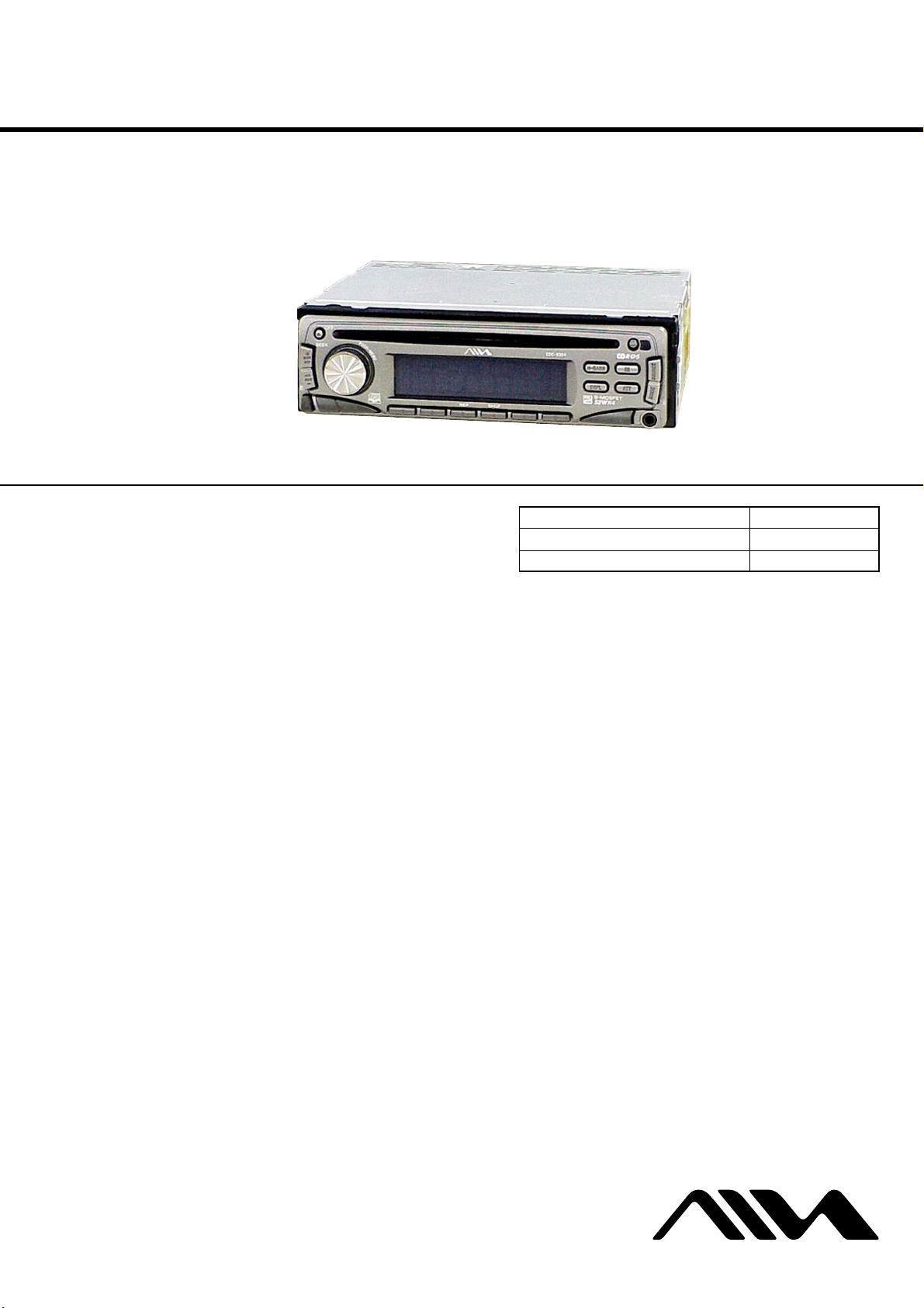
Photo: CDC-R304
• The tuner and CD sections have no adjustments.
• CDC-X304: US model/X444
AUDIO POWER SPECIFICATIONS
POWER OUTPUT AND TOTAL HARMONIC DISTORTION
23.2 watts per channel minimum continuous average power into
4 ohms, 4 channels driven from 20 Hz to 20 kHz with no more
than 5% total harmonic distortion.
US Model
Canadian Model
CDC-X204/X304/X444
AEP Model
UK Model
CDC-R304/X304
East European
Model
CDC-X104EE
Model Name Using Similar Mechanism CDX-R3000/R3000T
CD Drive Mechanism Type MG-611XC-186//Q
Optical Pick-up Name KSS1000E
• CDC-X204
AUDIO POWER SPECIFICATIONS
POWER OUTPUT AND TOTAL HARMONIC DISTORTION
22 watts per channel minimum continuous average power into
4 ohms, 4 channels driven from 20 Hz to 20 kHz with no more
than 5% total harmonic distortion.
Tuner section
FM
Tuning range US, Canadian Model:
87.5 – 107.9 MHz
AEP, UK Model:
87.5 – 108 MHz
CDC-X104EE:
FM1/FM2:
87.5 – 108.0 MHz
(at 50 kHz step)
FM3: 65 – 74 MHz
(at 30 kHz step)
Antenna terminal External antenna connector
Intermediate frequency 10.7 MHz/450 kHz
Usable sensitivity 9 dBf
Selectivity 75 dB at 400 kHz
Signal-to-noise ratio 67 dB (stereo),
69 dB (mono)
Harmonic distortion at 1 kHz
0.5% (stereo),
0.3% (mono)
Separation 35 dB at 1 kHz
Frequency response 30 – 15,000 Hz
AM (US, Canadian Model)
Tuning range 530 – 1,710 kHz
Antenna terminal External antenna connector
Intermediate frequency 10.7 MHz/450 kHz
Sensitivity 30 µV
SPECIFICATIONS
AM (CDC-X104EE)
Tuning range 531 – 1,602 kHz
Antenna terminal External antenna connector
Intermediate frequency 10.7 MHz/450 kHz
Sensitivity 30 µV
MW/LW (AEP, UK Model)
Tuning range MW: 531 – 1,602 kHz
LW: 153 – 279 kHz
Antenna terminal External antenna connector
Intermediate frequency 10.7 MHz/450 kHz
Sensitivity MW: 30 µV
LW: 40 µV
– Continued on next page –
FM/AM COMPACT DISC PLAYER
US, Canadian, East European model
FM/MW/LW COMPACT DISC PLAYER
AEP, UK model
9-877-519-01
2004A04-1
© 2004. 01
Sony Corporation
e Vehicle Company
Published by Sony Engineering Corporation
1
Page 2
CDC-R304/X104EE/X204/X304/X444
CD player section
Signal-to-noise ratio US, Canadian Model: 110 dB
AEP, UK Model/CDC-X444: 120 dB
Frequency response 10 – 20,000 Hz
Wow and flutter Below measurable limit
Power amplifier section
Outputs Speaker outputs
(sure seal connectors)
Speaker impedance 4 – 8 ohms
Maximum power output CDC-R304/X304/X444:
52 W × 4 (at 4 ohms)
CDC-X104EE/X204:
45 W × 4 (at 4 ohms)
General
Outputs Audio outputs terminal (rear/sub switchable)
Power antenna relay control terminal
Power amplifier control terminal
Inputs Telephone ATT control terminal (AEP, UK Model/
CDC-X444)
Antenna input terminal
Tone controls Low: ±10 dB at 60 Hz (HIP-HOP)
Mid: ±10 dB at 1 kHz (HIP-HOP)
High: ±10 dB at 10 kHz (HIP-HOP)
Power requirements 12 V DC car battery (negative ground)
Dimensions Approx. 178 × 50 × 176 mm
(7 1/8 × 2 × 7 in.) (w/h/d)
Mounting dimensions Approx. 182 × 53 × 161 mm
(7 1/4 × 2 1/8 × 6 3/8 in.) (w/h/d)
Mass Approx. 1.2 kg (2 lb. 10 oz.)
Supplied accessories Parts for installation and connections (1 set)
Front panel case (1)
Card remote control RM-Z304 (CDC-X444)
Design and specifications are subject to change without
notice.
TEST DISCS
This set can playback CD-R and CD-ROM discs. The following
test discs should be used to check the capability:
CD-R test disc TCD-R082LMT (Part No. J-2502-063-1)
CD-RW test disc TCD-W082L (Part No. J-2502-063-2)
• US, Canadian model
CAUTION
Use of controls or adjustments or performance of procedures
other than those specified herein may result in hazardous
radiation exposure.
• AEP, UK model
CAUTION
Use of controls or adjustments or performance of procedures other
than those specified herein may result in hazardous radiation
exposure.
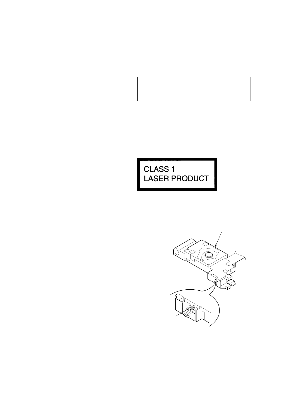
This compact disc player is classified as a CLASS 1 LASER
product. The CLASS 1 LASER PRODUCT label is located on the
exterior.
SERVICE NOTES
NOTES ON HANDLING THE OPTICAL PICK-UP BLOCK
OR BASE UNIT
The laser diode in the optical pick-up block may suffer electrostatic
breakdown because of the potential difference generated by the
charged electrostatic load, etc. on clothing and the human body.
During repair, pay attention to electrostatic breakdown and also use
the procedure in the printed matter which is included in the repair
parts.
The flexible board is easily damaged and should be handled with
care.
NOTES ON LASER DIODE EMISSION CHECK
The laser beam on this model is concentrated so as to be focused on
the disc reflective surface by the objective lens in the optical pickup block. Therefore, when checking the laser diode emission, observe from more than 30 cm away from the objective lens.
Notes on Chip Component Replacement
• Never reuse a disconnected chip component.
• Notice that the minus side of a tantalum capacitor may be dam-
aged by heat.
This label is located on the bottom of the chassis.
If the optical pick-up block is defective, please replace the whole
optical pick-up block.
Never turn the semi-fixed resistor located at the side of optical
pick-up block.
optical pick-up
semi-fixed resistor
SAFETY-RELATED COMPONENT WARNING!!
COMPONENTS IDENTIFIED BY MARK 0 OR DOTTED LINE
WITH MARK 0 ON THE SCHEMATIC DIAGRAMS AND IN
THE PARTS LIST ARE CRITICAL TO SAFE OPERATION.
REPLACE THESE COMPONENTS WITH SONY P ARTS WHOSE
PART NUMBERS APPEAR AS SHOWN IN THIS MANUAL OR
IN SUPPLEMENTS PUBLISHED BY SONY.
2
ATTENTION AU COMPOSANT AYANT RAPPORT
À LA SÉCURITÉ!!
LES COMPOSANTS IDENTIFIÉS P AR UNE MARQUE 0 SUR LES
DIAGRAMMES SCHÉMATIQUES ET LA LISTE DES PIÈCES
SONT CRITIQUES POUR LA SÉCURITÉ DE FONCTIONNEMENT.
NE REMPLACER CES COMPOSANTS QUE PAR DES PIÈCES
SONY DONT LES NUMÉROS SONT DONNÉS DANS CE MANUEL
OU DANS LES SUPPLÉMENTS PUBLIÉS PAR SONY.
Page 3
CDC-R304/X104EE/X204/X304/X444
D
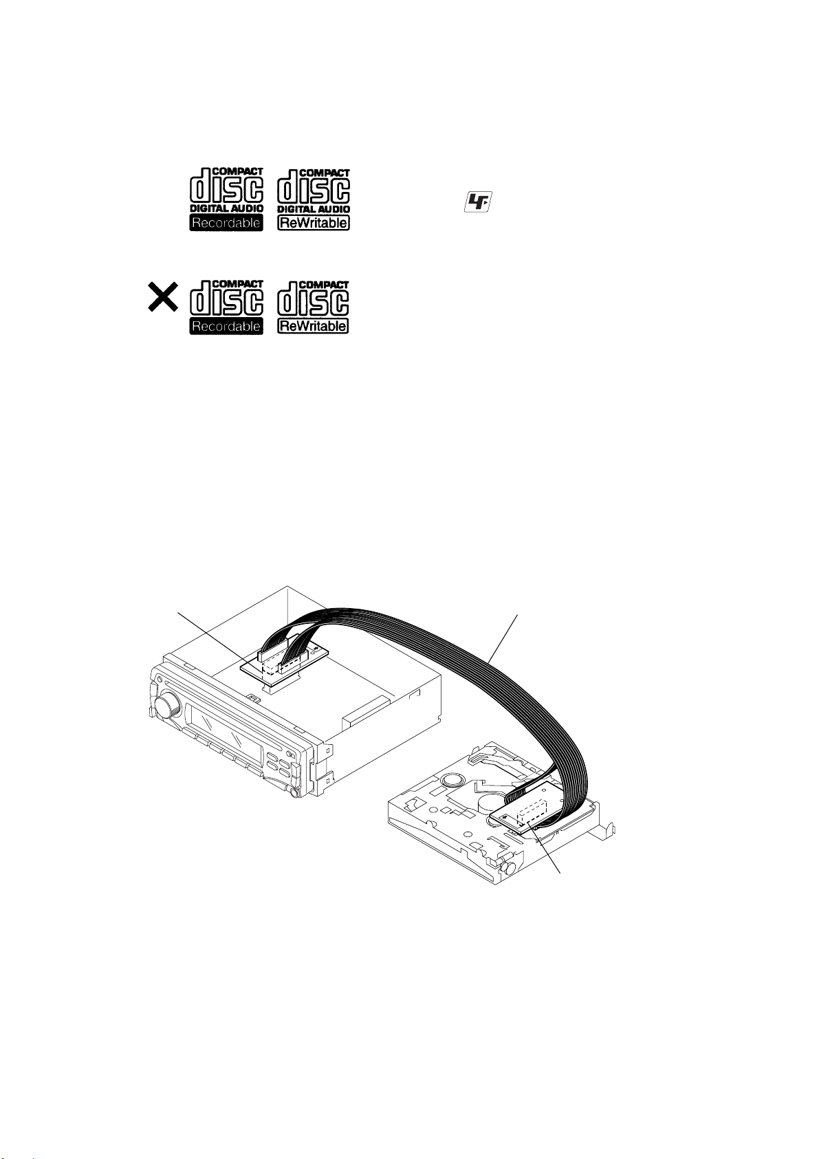
Notes on CD-R/CD-RW discs
• You can play CD-Rs (recordable CDs)/CD-RWs (rewritable CDs)
designed for audio use on this unit.
Look for these marks to distinguish CD-Rs/CD-RWs for audio
use.
These marks denote that a disc is not for audio use.
• Some CD-Rs/CD-RWs (depending on the equipment used for
its recording or the condition of the disc) may not play on this
unit.
• You cannot play a CD-R/CD-RW that is not finalized∗.
∗ A process necessary for a recorded CD-R/CD-RW disc to be
played on the audio CD player.
EXTENSION CABLE AND SERVICE POSITION
When repairing or servicing this set, connect the jig (extension cable)
as shown below.
z
UNLEADED SOLDER
Boards requiring use of unleaded solder are printed with the lead
free mark (LF) indicating the solder contains no lead.
(Caution: Some printed circuit boards may not come printed with
the lead free mark due to their particular size.)
: LEAD FREE MARK
Unleaded solder has the following characteristics.
• Unleaded solder melts at a temperature about 40°C higher than
ordinary solder.
Ordinary soldering irons can be used but the iron tip has to be
applied to the solder joint for a slightly longer time.
Soldering irons using a temperature regulator should be set to
about 350°C.
Caution: The printed pattern (copper foil) may peel away if the
heated tip is applied for too long, so be careful!
• Strong viscosity
Unleaded solder is more viscous (sticky, less prone to flow)
than ordinary solder so use caution not to let solder bridges
occur such as on IC pins, etc.
• Usable with ordinary solder
It is best to use only unleaded solder but unleaded solder may
also be added to ordinary solder.
• Connect the MAIN board (CN301) and the SERVO board (CN1)
with the extension cable (Part No. J-2502-076-1).
MAIN BOARD
CN301
J-2502-076-1
SERVO BOAR
CN1
3
Page 4

CDC-R304/X104EE/X204/X304/X444
TABLE OF CONTENTS
1. GENERAL
Location of Controls................................................................ 5
Connections (US, Canadian Model)........................................ 6
Connections (AEP, UK Model) ............................................... 7
2. DISASSEMBLY
2-1. Sub Panel Assy.................................................................... 9
2-2. CD Mechanism Block ......................................................... 9
2-3. Main Board ....................................................................... 10
2-4. Chassis (T) Sub Assy ........................................................ 10
2-5. Roller Arm Assy ................................................................ 11
2-6. Chassis (OP) Assy............................................................. 11
2-7. Optical Pick-up ................................................................. 12
2-8. SL Motor Assy (M902) .....................................................12
2-9. LE Motor Assy (M903)..................................................... 13
2-10. Servo Board....................................................................... 13
3. DIAGRAMS
3-1. IC Pin Descriptions ........................................................... 14
3-2. Block Diagram –CD Section–........................................... 18
3-3. Block Diagram –Main Section–........................................ 19
3-4. Block Diagram –Display Section–.................................... 20
3-5. Circuit Boards Location .................................................... 20
3-6. Note for Printed Wiring Boards and
Schematic Diagrams ..........................................................21
3-7. Waveforms ......................................................................... 21
3-8. Printed Wiring Boards –CD Mechanism Section–............ 22
3-9. Schematic Diagram –CD Mechanism Section– ................23
3-10. Schematic Diagram –Main Section (1/2)– ........................24
3-11. Schematic Diagram –Main Section (2/2)– ........................25
3-12. Printed Wiring Board –Main Section– ..............................26
3-13. Printed Wiring Boards –Display Section– ........................ 27
3-14. Schematic Diagram –Display Section–............................. 28
3-15. IC Block Diagrams............................................................ 29
4. EXPLODED VIEWS
4-1. Main Section ..................................................................... 32
4-2. Front Panel Section ........................................................... 33
4-3. CD Mechanism Section (1) ...............................................34
4-4. CD Mechanism Section (2) ...............................................35
4-5. CD Mechanism Section (3) ...............................................36
4-6. CD Mechanism Section (4) ...............................................37
5. ELECTRICAL PARTS LIST ........................................ 38
4
Page 5
LOCATION OF CONTROLS
SECTION 1
GENERAL
CDC-R304/X104EE/X204/X304/X444
This section is extracted
from instruction manual.
5
Page 6
CDC-R304/X104EE/X204/X304/X444
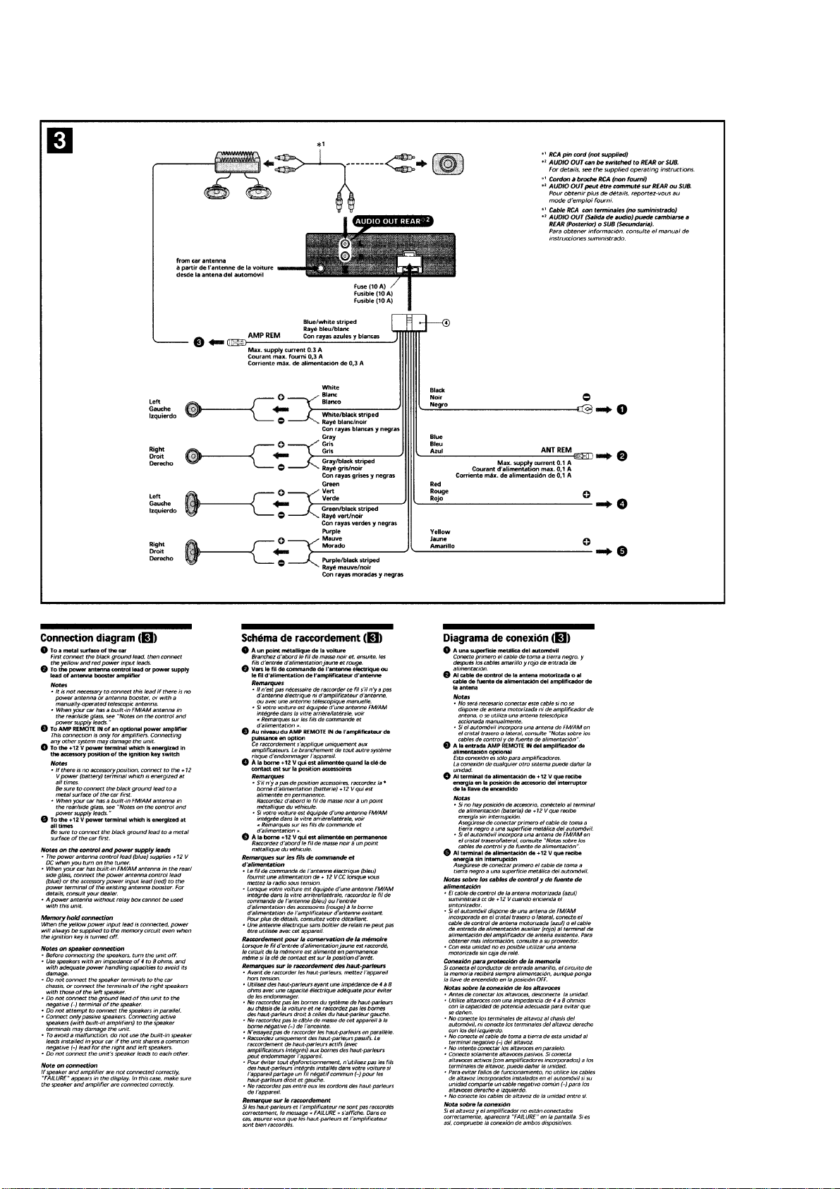
CONNECTIONS (US, Canadian Model)
6
Page 7
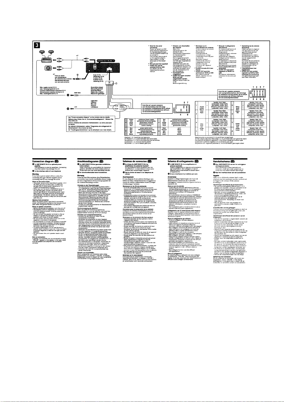
CONNECTIONS (AEP, UK Model)
CDC-R304/X104EE/X204/X304/X444
7
Page 8
CDC-R304/X104EE/X204/X304/X444
SECTION 2
DISASSEMBLY
Note : This set can be disassemble according to the following sequence.
SET
2-1. SUB PANEL ASSY
(Page 9)
2-2. CD MECHANISM BLOCK
(Page 9)
2-3. MAIN BOARD
(Page 10)
2-7. OPTICAL PICK-UP
(Page 12)
2-4. CHASSIS (T) SUB ASSY
(Page 10)
2-5. ROLLER ARM ASSY
(Page 11)
2-6. CHASSIS (OP) ASSY
(Page 11)
2-8. SL MOTOR ASSY (M902)
(Page 12)
2-10. SERVO BOARD
(Page 13)
2-9. LE MOTOR ASSY (M903)
(Page 13)
8
Page 9
Note : Follow the disassembly procedure in the numerical order given.
s
)
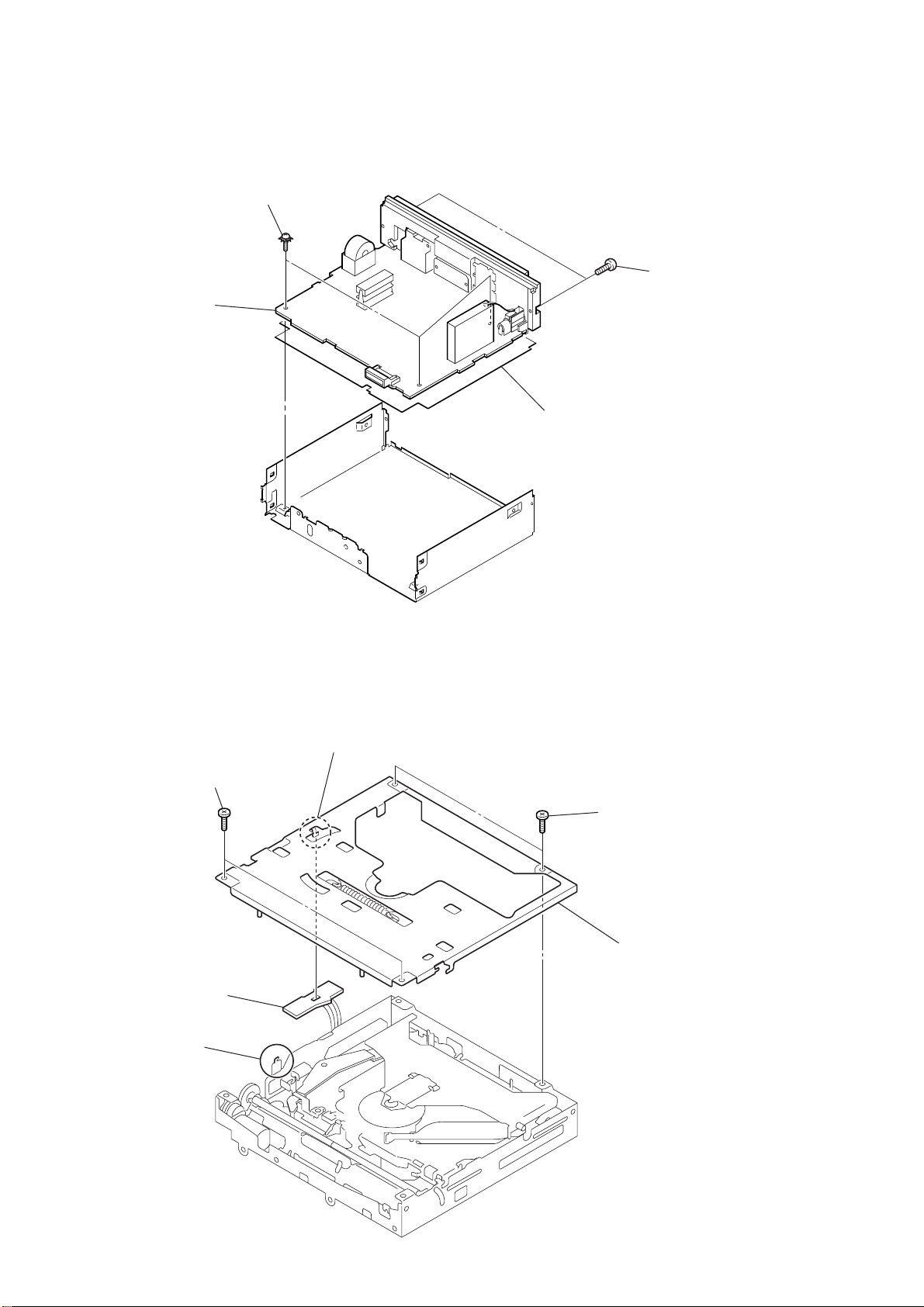
2-1. SUB PANEL ASSY
3
two claws
CDC-R304/X104EE/X204/X304/X444
1
two
screws
(+PTT 2.6
x
6)
2-2. CD MECHANISM BLOCK
5
CD mechanism block
4
sub panel assy
7
bracket (CD)
6
two
screws
(+PTT 2.6
2
two claw
x
4)
2
screw
(+PTT 2.6
x
6)
3
4
CN301
1
screw
(+PTT 2.6
x
6
9
Page 10
CDC-R304/X104EE/X204/X304/X444
)
2-3. MAIN BOARD
1
three ground point screws
3
MAIN board
(+PTT 2.6
x
6)
insulating sheet
2
two
screws
(+PTT 2.6
x
6
2-4. CHASSIS (T) SUB ASSY
2
two
screws
(+P 1.7
5
SENSOR board
3
claw
x
2.2)
4
claw
1
two
screws
x
(+P 1.7
6
2.2)
chassis (T) sub assy
10
Page 11
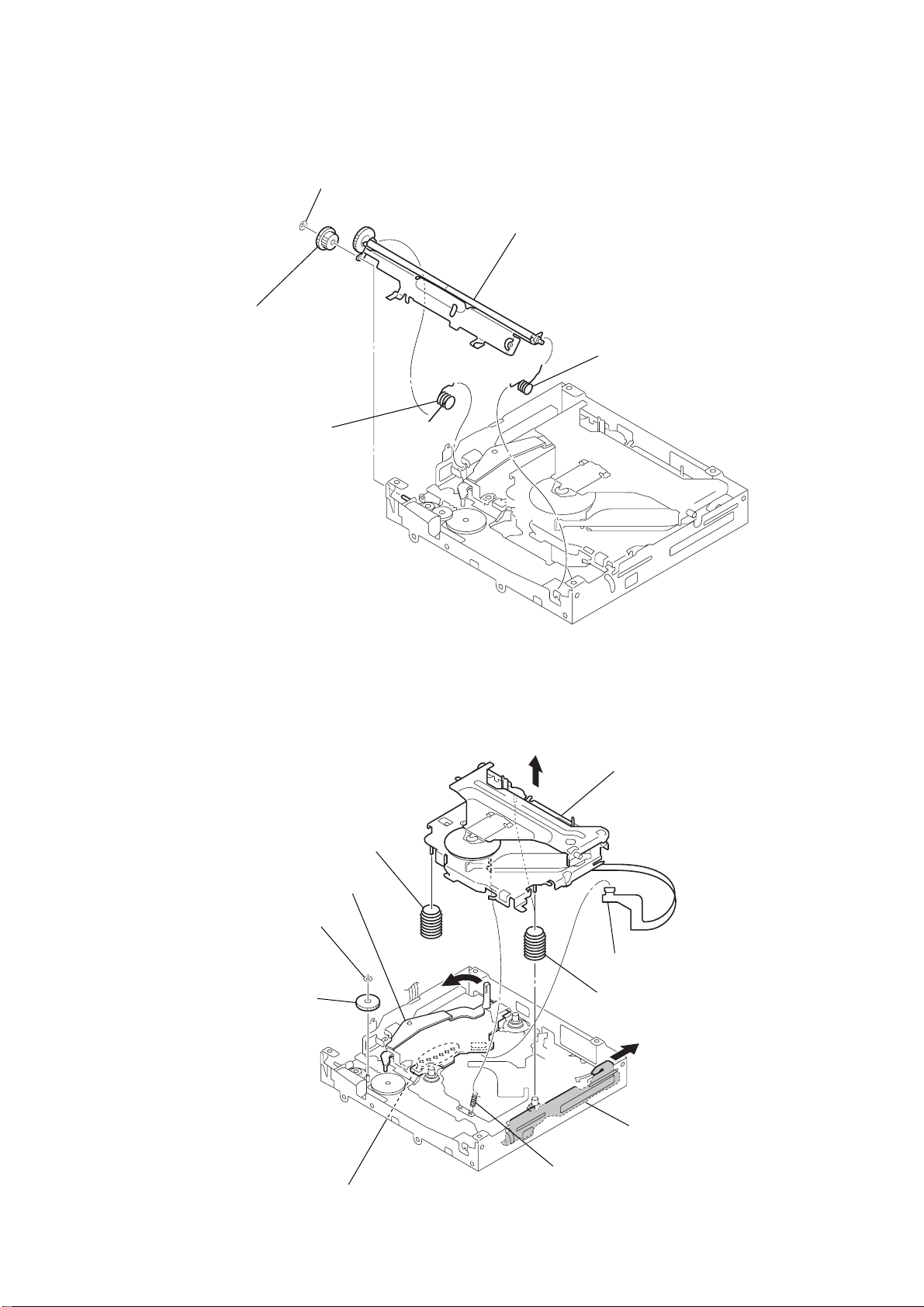
2-5. ROLLER ARM ASSY
4
worm wheel (RA)
1
spring (RAL)
3
washer (0.8-2.5)
CDC-R304/X104EE/X204/X304/X444
5
roller arm assy
2
spring (RAR)
2-6. CHASSIS (OP) ASSY
0
coil spring (damper)
4
washer
5
gear (LE1)
lever (D)
6
8
qa
chassis (OP) assy
1
CN2
9
two coil springs (damper)
7
slider (R)
2
Remove the six solderings.
3
tension coil spring (KF)
11
Page 12
CDC-R304/X104EE/X204/X304/X444
)
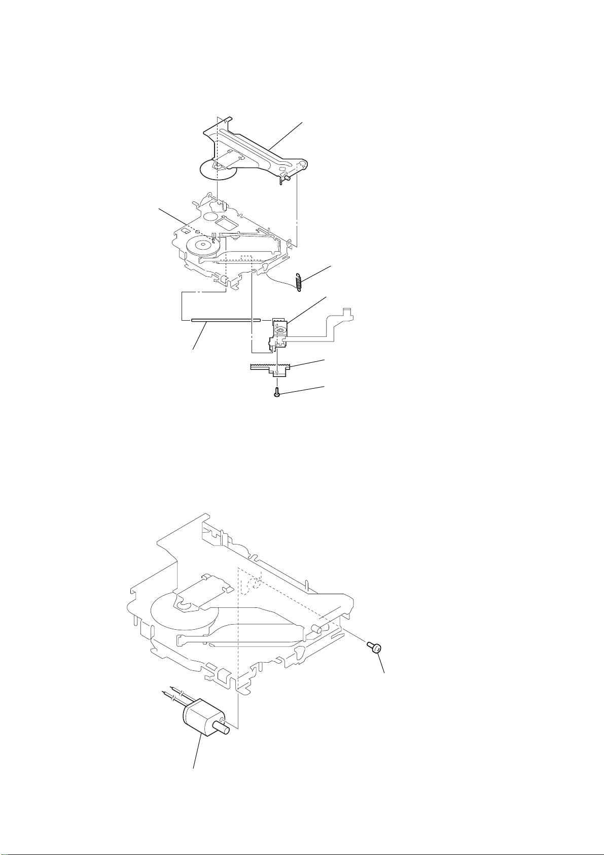
2-7. OPTICAL PICK-UP
5
claw
2
chucking arm sub assy
1
tension coil spring (CHKG
7
optical pick-up
2-8. SL MOTOR ASSY (M902)
6
main shaft
4
rack (SL)
3
screw
(+B 1.4
x
5)
12
2
SL motor assy (M902)
1
screw
(+P 1.4
x
1.8)
Page 13
2-9. LE MOTOR ASSY (M903)
qf
two toothed lock
(+M 1.4
bracket (LEM)
qs
(+M 1.7
screw
x
)
screws
2.5)
6
screw
(+P 1.7
x
qd
2.2)
qa
screw
(+M 1.7
qg
(M903)
0
woam (LEB) assy
x
2.5)
LE motor assy
7
leaf spring (LE)
CDC-R304/X104EE/X204/X304/X444
8
screw
x
(+M 1.7
9
bearing (LEB)
2
washer
3
2.5)
gear (LE1)
lever (D)
4
5
slider (R)
2-10. SERVO BOARD
1
Remove the eight solderings.
1
Remove the soldering.
6
SERVO board
2
Remove the three solderings.
4
toothed lock
(M 1.7)
5
screw
claw
3
CN2
13
Page 14

CDC-R304/X104EE/X204/X304/X444
SECTION 3
DIAGRAMS
3-1. IC PIN DESCRIPTIONS
• IC1 µPD63712GC-8EU-A (RF AMP, DIGITAL SERVO, DIGITAL SIGNAL PROCESSOR) (SERVO BOARD)
Pin No. Pin Name I/O Pin Description
1LDOLaser diode ON/OFF control signal output (L: laser OFF, H: laser ON)
2PDIDimmer monitor input from optical pick-up laser diode.
3PNINot used. (Fixed at L in this set)
4AVDD — Analog power supply pin (+3.3 V)
5 DGND — Ground
6 RFOK O RFOK signal output to system control IC.
7 INTQ O CD text pack synchronization signal output to system control IC.
8 RST I CD reset signal input from system control IC.
9A0I
10 STB I Data strobe signal input from system control IC.
11 SCK I Serial clock input from system control IC.
12 SO O Serial data output to system control IC.
13 SI I Serial data input from system control IC.
14 DVDD — Power supply pin (+3.3 V)
15 DAVDD — D/A converter power supply (+) pin (+3.3 V)
16 ROUT O Analog audio signal output (R-ch)
17 DAGND — Ground
18 REGC — Capacitor connection pin for SCF regulator.
19 DAGND — Ground
20 LOUT O Analog audio signal output (L-ch)
21 DAVDD — D/A converter power supply (+) pin (+3.3 V)
22 XVDD — Power supply pin (+3.3 V)
23 XTAL O Main system clock output (16.9344 MHz)
24 XTAL I Main system clock input (16.9344 MHz)
25 XGND — Ground
26 DVDD — Power supply pin (+3.3 V)
27 C1D1/FZD O Not used. (Open)
28 C1D2/TZD O Not used. (Open)
29 C2D1/RMUTE O CD R-ch data zero detection signal output
30 C2D2/LMUTE O CD L-ch data zero detection signal output
31 C2D3/SHOCK/SBSY O Not used. (Open)
32 LOCK/FR O Not used. (Open)
33 WFCK/MIRR O Not used. (Open)
34 RFCK/HOLD O Not used. (Open)
35 PLCK O Not used. (Open)
36 C16M O Not used. (Open)
37 DGND — Ground
38 TX O Not used. (Open)
39 EMPH/RAMOVER O Not used. (Open)
40 FLAG O Not used. (Open)
41 DVDD — Power supply pin (+3.3 V)
42 LIMIT I Not used. (Fixed at L in this set)
43 XTALEN I
44 DGND — Ground
45 DIN I Not used. (Connect to DOUT in this set)
46 DOUT O Not used. (Connect to DIN in this set)
47 SCKIN I Not used. (Connect to SCKO in this set)
48 SCKO O Not used. (Connect to SCKIN in this set)
49 LRCKIN I Not used. (Connect to LRCK in this set)
Command/parameter discrimination signal input from system control IC.
(L: command transmission, H: parameter transmission)
Oscillation circuit ON/OFF control signal input (L: ON, H: OFF)
(Fixed at L in this set)
14
Page 15

CDC-R304/X104EE/X204/X304/X444
Pin No. Pin Name I/O Pin Description
50 LRCK O Not used. (Connect to LRCKIN in this set)
51 DVDD — Power supply pin (+3.3 V)
52 FD+ O Focus servo drive PWM signal output (+)
53 FD– O Focus servo drive PWM signal output (–)
54 TD+ O Tracking servo drive PWM signal output (+)
55 TD– O Tracking servo drive PWM signal output (–)
56 SD+ O Sled servo drive PWM signal output (+)
57 SD– O Sled servo drive PWM signal output (–)
58 MD+ O Spindle servo drive PWM signal output (+)
59 MD– O Spindle servo drive PWM signal output (–)
60 DGND — Ground
61 TESTEN I Test setting input (Fixed at L in this set)
62 to 66 TEST4 to TEST0 I Test setting input (Fixed at L in this set)
67 ADGND — A/D converter power supply (–) pin
68 EFM O EFM signal output
69 ASY I EFM comparator reference voltage input
70 ADVDD — A/D converter power supply pin (+3.3 V)
71 RFI I RF signal input for EFM data growing.
72 EQ2 — Not used. (Open)
73 EQ1 — RF amplifier equalizer parts connection pin
74 RF– I Not used. (Open)
75 RF2– I RF amplifier inversion input
76 AGCO O RF signal output after on AGC.
77 AGCI I RF AGC signal amplifier input
78 RFO O RF signal output before on AGC.
79 ATEST I Not used. (Open)
80 C3T — Capacitor connection pin for 3T detection.
81 AGND — Ground
82 A I Signal input (A) from optical pick-up detector.
83 C I Signal input (C) from optical pick-up detector.
84 B I Signal input (B) from optical pick-up detector.
85 D I Signal input (D) from optical pick-up detector.
86 F I Signal input (F) from optical pick-up detector.
87 E I Signal input (E) from optical pick-up detector.
88 VREFIN I Reference voltage (+1.65 V) input
89 AVDD — Analog power supply pin (+3.3 V)
90 REFOUT O Reference voltage (+1.65 V) output
91 REFC — Capacitor connection pin for reference voltage output.
92 FE– I Focus error signal amplifier inversion input
93 FEO O Focus error signal amplifier output
94 ADCIN I Not used. (Open)
95 TE- I Tracking error signal amplifier inversion input
96 TEO O Tracking error signal amplifier before output
97 TE2 O Tracking error signal amplifier after output
98 TEC I Tracking error signal comparator input
99 AGND — Ground
100 PWMSW I Not used. (Fixed at L in this set)
15
Page 16

CDC-R304/X104EE/X204/X304/X444
• IC501 MN101E01KAB (SYSTEM CONTROL) (MAIN BOARD (1/2))
Pin No. Pin Name I/O Pin Description
1DAVDD — Power supply pin for D/A output converter (+3.3 V)
2 BBE-MP O Not used in this set. (Open)
3DAVSS — Ground pin for D/A output converter
4 to 6 NCO O Not used in this set. (Open)
7 UNISO O SONY-BUS data signal output Not used in this set. (Open)
8 UNISI I SONY-BUS data signal input Not used in this set.
9 UNICKO O SONY-BUS clock signal output Not used in this set.
10 VDD1 — Power supply pin for internal core (+3.3 V)
11 MMOD I Flash microcomputer write detection signal input Not used in this set.
12 OSCOUT O High speed operation clock signal output (27 MHz)
13 OSCIN I High speed operation clock signal input (27 MHz)
14 VSS1 — Ground pin for internal core
15 XIN I Low speed operation clock signal input (32.768 kHz)
16 XOUT O Low speed operation clock signal output (32.768 kHz)
17 VDD2 — Power supply pin for internal core (+3.3 V)
18 MOD1 — Pull up: “H”
19 RESET I Reset signal input
20 NCO O Not used in this set. (Open)
21 ACC IN I Accessory power supply detection signal input
22 TEST IN I Test mode detection signal input
23 TEL ATT I Telephone attenuate detection signal input
24 ATT O Audio mute control signal output
25 XKEYON O Key power supply control signal output Not used in this set. (Open)
26 NCO O Not used in this set. (Open)
27 KEYACK I Key acknowledge detection signal input
28 TU ATTIN I Tuner mute ZERO cross detection signal input
29, 30 NCO O Not used in this set. (Open)
31 BUIN I Back up power supply detection signal input
32 CD INTQ I CD servo IC CD text pack synchronization signal input
33 CD SO O CD servo IC serial data signal output (for command/text)
34 CD SI I CD servo IC serial data signal input (for command/text)
35 CD SCK O CD servo IC serial clock signal output (for command/text)
36 BUSON O BUS on signal output
37 SYSRST O System reset signal output
38 CD RFOK I CD servo IC RFOK signal input
39 CD RST O CD servo IC reset signal output
40 CD A0 O
41 CD STB O CD servo IC data strob signal output
42 CD MUTE R I Mechadeck mute zero cross detection signal input R
43 CD MUTE L I Mechadeck mute zero cross detection signal input L
44 CD INSW I CD mecha disc in switch detection signal input
45 CD SELFSW I CD mecha self load position detection switch signal input
46 CD LM LO O CD mecha loading motor control signal output
47 CD LM EJ O CD mecha eject motor control signal output
48 CD DSW I CD mecha down switch detection signal input
49 CD LIMIT I CD mecha in-limit switch signal input
50 NCO O Not used in this set. (Open)
51 AREASEL1 I Destination function setting input 1
52 AREASEL2 I Destination function setting input 2
53 AREASEL3 I Destination function setting input 3
CD servo IC command/parameter identification signal output
Command transmission: “L”, Parameter transmission: “H”
16
Page 17

Pin No. Pin Name I/O Pin Description
54 LCD CTL O
55, 56 NCO O Not used in this set. (Open)
57 DSSA O DSSA on/off change signal output (Cut off rear)
58 PANEL SW I Front panel attachment detection signal input “L”: with panel, “H”: without panel
59 DIAG I Condition signal input from the power IC
60 VOLATT O Electronic volume attenuate control signal output
61, 62 NCO O Not used in this set. (Open)
63 VSS2 — Ground pin for I/O port
64 TU ATT O Tuner mute control signal output
65 NCO O Not used in this set. (Open)
66 NS MASK O Noise mask signal output
67 EEP CKO O Serial clock signal output for EEPROM communication
68 EEP SIO I/O Serial data signal input/output for EEPROM communication
69 NCO O Not used in this set. (Open)
70 AMPSTB O Power regulator IC standby signal output
71 to 73 NCO O Not used in this set. (Open)
74 NCO O Not used in this set. (Open)
75 COL SEL I
76 LCDSO O Serial data signal output to the LCD driver
77 LCDCE O Chip enable signal output to the LCD driver
78 LCDCKO O Serial clock signal output to the LCD driver
79 I2C SIO I/O I2C BUS serial data signal input/output
80 NCO O Not used in this set. (Open)
81 I2C CKO O I2C BUS serial clock signal output
82 DAVN I RDS data block synchronization detection signal input
83 SIRCS I Remote control signal input
84 NCO O Not used in this set. (Open)
85 BEEP O Beep signal output to the power amp
86 to 88 NCO O Not used in this set. (Open)
89 VDD3 — Power supply pin for I/O port (+3.3 V)
90 COL SW I
91 VSS3 — Ground pin for I/O port
92 QUALITY I Noise detection signal input
93 VSM I S meter voltage detection signal input
94 KEYIN1 I Key signal input 1
95 KEYIN0 I Key signal input 0
96 NCO O Not used in this set.
97 KEYIN2 I Key signal input (EJECT, OFF, SOURCE switch)
98 RE I Rotary encoder signal input
99 L METER I Level meter voltage detection signal input
100 VREF+ — Power supply pin for A/D input converter
“H” output: LCD unit and key confusion, power off
“L” output: LCD unit and key confusion, power on
“H”: Front panel illumination green (Initial value)
“L”: Front panel illumination amber (Initial value)
“L” input: two color change/initial slave color: amber
“H” input: one color/slave color: white
CDC-R304/X104EE/X204/X304/X444
17 17
Page 18

CDC-R304/X104EE/X204/X304/X444
3-2. BLOCK DIAGRAM — CD SECTION —
DETECTOR
PD1
PD2
PD1
PD2
I-V AMP
• R-ch is omitted due to same as L-ch.
• Siganal Path
: CD PLAY
AGCO
82
B
84
C
83
D
85
78
RFO
A
AGCI
77
76
RF AMP,DIGITAL SERVO,
DIGITAL SIGNAL PROCESSOR
71
IC1
EFM
RFI
68
ASY
69
LOUT
ROUT
LMUTE
RMUTE
20
16
R-CH
30
29
43
42
CD MUTE L
CD MUTE R
CD-L
MAIN
A
SECTION
(Page 19)
E
F
LASER DIODE
PICK-UP BLOCK
(KSS1000E)
2-AXIS DEVICE
(FOCUS)
(TRACKING)
PD LD
OPTICAL
PD
FCS+
FCS–
TRK+
TRK–
E
F
LD
AUTOMATIC
POWER
CONTROL
M902
(SLED)
Q1
M
87
86
1
FOCUS/TRACKING COIL DRIVE,
11
12
13
14
15
16
FEO
E
F
LD
SLED/SPINDLE/LOADING
VO2–
VO2+
VO1–
VO1+
VO4+
VO4–
93
TEO
96
PD
MOTOR DRIVE
IC2
2
OPIN2+
OPIN2–
OPIN1+
OPIN1–
OPIN4+
OPIN4–
FE–
92
TE2
TE–
95
5
6
2
3
27
26
97
TEC
98
12
SO
13
SI
11
SCK
6
RFOK
7
INTQ
10
STB
9
A0
8
RST
23
FD+
52
FD–
53
TD+
54
TD–
55
SD+
56
SD–
57
XTAL
XTAL
24
X1
16.934MHz
SW1
(DOWN)
SW2
(SELF)
SW3
(DISC IN)
CD_SI
34
CD_SO
33
CD_SCK
35
CD RFOK
38
CD INTQ
32
CD STB
41
CD_A0
40
39
CD RST
CD_DSW
48
CD_SELFSW
45
CD_INSW
44
SYSTEM CONTROL
IC501 (1/3)
M901
(SPINDLE)
M903
(LOADING)
OPIN3+
OPIN3–
FWD
REV
24
23
1
28
17
M
M
VO3+
18
VO3–
10
VOL+
9
VOL–
MD+
58
MD–
59
SW4
(LIMIT)
49
46
47
CD_LIMIT
CD LM LO
CD LM EJ
1818
Page 19

3-3. BLOCK DIAGRAM — MAIN SECTION —
J601
(AUX IN)
TU1
(TUNER UNIT)
J1
(ANTENNA)
1
ANT
VCC
TU VDD
E2P VDD
TU-SCL
TU-SDA
RDS
MULTI
CONDITION
QUALITY
S-METER
TU MUTE
E2P SCL
E2P SDA
L
R
4
3
10
11
15
13
14
9
8
5
6
7
16
17
AUDIO+8.3V
TU+5V
BACK UP+3.3V
SCL
SDA
X51
8.664MHz
RDS DEMODULATOR
MPX
16
XTI
9
XTO
10
R304
IC51
1
R-CH
CD
SECTION
(Page 18)
SCL
SDA
INTN
VDDDVDDA
7
SCL
11
SDA
12
15
CD-L
A
LEVEL METER
VOLTAGE DETECT
D401,402,Q401
B+ SWITCH
Q51,52
R304
NS MASK
SWITCH
Q3
R-CH
R-CH
BACK UP
+3.3V
SOUND CONTROL,
ELECTRONIC VOLUME
IC401
5
AUX-LCH
3
AUX-RCH
OUT SUB L
OUT SUB R
9
CD-LCH
8
CD-RCH
7
TU-LCH
6
15
16
99
82
28
92
66
93
64
67
68
OUT-FL
TU-RCH
OUT-RL
OUT-FR
OUT-RR
OUT-SEL-R
OUT-SEL-L
SYSTEM CONTROL
IC501 (2/3)
I2C SCK
I2C SIO
L METER
VOL ATT
AMPSTB
DAVM
ACC IN
TEL ATT
TU ATTIN
TEST IN
QUALITY
NS MASK
VSM
TU ATT
EEP CKO
EEP SIO
BUS ON
SYS RST
MUTE
SCL
SDA
ATT
BEEP
DIAG
DSSA
BUIN
17
18
23
22
25
24
29
30
31
81
79
60
24
85
70
59
57
21
23
22
31
36
37
R-CH
R-CH (FRONT)
R-CH (REAR)
SCL
SDA
SCL
SDA
BATTERY
CHECK
Q582
REAR L/R
CUT OFF
SWITCH
Q403
DSSA ON/OFF
SWITCH
Q402
MUTE DRIVE
Q491,492
LOW VOLTAGE
DETECT
Q581
MUTE
Q481
MUTE
Q431
OVER VOLTAGE
MUTE
Q451
D491,492
DETECT
Q580
BATT
SDA
SCL
BATT
R304/X104EE/X304:
AEP,UK MODEL
TU+5V
MULTIPLE VOLTAGE
12
IN-FL
11
IN-RL
2
SDA
4
SCL
16
BEEP
22
STB
25
DIAG
35
VP
TU+5V REG
Q1
D580
D581
POWER AMP
REGULATOR
IC750
AUDIO+8.3V
SERVO+3.3V
MECHA+6V
ACC CHECK
TEL ATT
BATT
CDC-R304/X104EE/X204/X304/X444
OUT-FL+
5
OUT-FL–
3
9
OUT-RL+
7
OUT-RL–
AMP-REM
29
ANT-REM
27
BATT
30
B.UP+B
PANEL+B
Q631
Q651
AUDIO+8.3V
AUDIO+8.3V
37
BACK UP+3.3V
31
SERVO+3.3V
33
MECHA+6V
34
PANEL+10V
• R-CH is omitted due to same as L-CH.
• Signal Path
: CD PLAY
: FM
: AM/MW/LW
: AUX
R-CH
R-CH
FU601
CN601
10
12
11
16
13
15
1
FL+
9
FL–
2
RL+
RL–
4
FR+
FR–
3
RR+
RR–
5
AMP-REM
6
ANT-REM
BATT
7
ACC
ATT
TEST
L
R
J331
AUDIO OUT
REAR
19 19
Page 20

CDC-R304/X104EE/X204/X304/X444
t
3-4. BLOCK DIAGRAM — DISPLAY SECTION — 3-5. CIRCUIT BOARDS LOCATION
BACK UP+3.3V
ROTARY
ENCODER
S911 (1/2)
KEY MATRIX
S901-903
KEY MATRIX
S904-910
S911 (2/2)
KEY MATRIX
S912-920
X104EE/X304:
US,CND MODEL
RESET
IC602
2
IN
R304/X204/
X304/X444
OUT
1
BACK UP
+3.3V
S702
RESET
SYSTEM CONTROL
IC501 (3/3)
RE
98
KEYIN2
97
KEYACK
27
KEYIN1
94
KEYIN0
95
COL SEL
75
COL SW
90
RESET
19
LCD SO
LCD CKO
LCD CE
LCD CTL
SIRCS
76
78
77
54
X444
83
LCD DRIVER
IC901
64
DI
CLK
63
CL
CE
62
CE
DIMMER
DIMMER
REMOTE CONTROL
SIGNAL RECEIVER
IC971
2
SEG3
|
SEG50
COM1
|
COM4
VCC
OUT
SERVO board
3
|
50
54
|
51
1
LCD901
CRYSTAL
DISPLAY
DIMMER
CONTROL
Q901
LIQUID
PANEL
LED921,922
LCD
()
BACK LIGHT
SENSOR board
tuner uni
(TU1)
PANEL+10V
LED901-920
PANEL+3.3V
SWITCH
1
IR
Q503
BUCK UP+3.3V
KEY board
MAIN board
AUX board
X502
32.768kHz
XIN
15
XOUT
16
OSCIN
OSCOUT
13
12
X501
27MHz
2020
Page 21

CDC-R304/X104EE/X204/X304/X444
3-7. WAVEFORMS3-6. NOTE FOR PRINTED WIRING BOARDS AND SCHEMATIC DIAGRAMS
THIS NOTE IS COMMON FOR PRINTED WIRING
BOARDS AND SCHEMATIC DIAGRAMS.
(In addition to this, the necessary note is printed
in each block.)
For schematic diagrams.
Note:
• All capacitors are in µF unless otherwise noted. pF: µµF
50 WV or less are not indicated except for electrolytics
and tantalums.
• All resistors are in Ω and 1/
specified.
f
•
• C : panel designation.
• A : B+ Line.
• B : B– Line.
• H : adjustment for repair.
•Voltages and waveforms are dc with respect to ground
• CD mechanism section
no mark : CD PLAY
• Main (1/2), (2/2) and Display sections
no mark : FM
: internal component.
Note:
The components identified by mark 0 or dotted
line with mark 0 are criti-
cal for safety.
Replace only with part
number specified.
under no-signal (detuned) conditions.
(): AM
<>: CD PLAY
4
W or less unless otherwise
Note:
Les composants identifiés par
une marque 0 sont critiques
pour la sécurité.
Ne les remplacer que par une
piéce portant le numéro
spécifié.
∗ : Impossible to measure
•Voltages are taken with a VOM (Input impedance 10 MΩ).
Voltage variations may be noted due to normal production tolerances.
•Waveforms are taken with a oscilloscope.
Voltage variations may be noted due to normal production tolerances.
• Circled numbers refer to waveforms.
• Signal path.
J : CD PLAY
F : FM
f : AM/MW/LW
a : AUX
• Abbreviation
CND : Canadian model.
For printed wiring boards.
Note:
• X : parts extracted from the component side.
• Y : parts extracted from the conductor side.
a
•
• : Pattern from the side which enables seeing.
(The other layers' patterns are not indicated.)
Caution:
Pattern face side: Parts on the pattern face side seen from the
(Side B) pattern face are indicated.
Parts face side: Parts on the parts face side seen from the
(Side A) parts face are indicated.
• Abbreviation
: Through hole.
C
Q
These are omitted
EB
E
CB
These are omitted
C
BE
These are omitted
CND : Canadian model.
— Servo Board —
(MODE: CD PLAY)
1
16.9344MHz
IC1 wd (XTAL)
2
uj
(AGCI)
IC1
3
Approx. 620mVp-p
od
(FEO)
IC1
4
Approx. 200mVp-p
oh
(TEO)
IC1
1.2Vp-p
1.6Vp-p
0V
0V
— Main Board —
1
27MHz
IC501 qs (OSCOUT)
2
32.768kHz
qg
(XIN)
IC501
3
q;
(XTO)
IC51
2.2Vp-p
1.8Vp-p
0.9Vp-p
21 21
Page 22

CDC-R304/X104EE/X204/X304/X444
3-8. PRINTED WIRING BOARDS — CD MECHANISM SECTION — • Refer to page 20 for Circuit Boards Location. : Uses unleaded solder.
A
B
C
D
1
234567891011121314
C6
R42
C5
C3
R44
R45
R41
C7
IC1
R6
C19
FB1
R7
C18
C1
C21
C23
R9
C32
C27
C25
C36
C26
C31
C30
R13
C29
C28
C39
C38
Q1
R15
R11
R14
C34
R12
C37
C35
CN2
CN1
(Page 26)
C2
C20
JR91
JR90
JR40
C13
JR41
C11
C8
X1
R1
C17
E
F
G
R74
R76
R72
R77
R70
R75
R71
R73
C73
C72
C71
C75
C70
IC2
C78
C77
C76
C74
C79
R83
R85
R84
R81
R79
R82
R80
R78
SW1
SW3
SW2
1-688-822-
2222
Page 23

• Refer to page 21 for Waveforms.
3-9. SCHEMATIC DIAGRAM — CD MECHANISM SECTION — • Refer to page 29 for IC Block Diagram.
CDC-R304/X104EE/X204/X304/X444
C20
SW3
SW2
TP19 C18
CN2
TP27
TP28
TP29
TP31
TP30
TP29
TP14
TP28
TP27
TP26
Q1
C36
R13
C37
R12
C35
C34
R11
SW4
TP81
TP80
M901
M902
SW1
TP85
TP83
TP84
TP82
TP87
TP88
TP89
TP90
TP91
R14 R15
C38
TP33TP32
C39
TP22
TP20
C26
TP21
C27
C28
TP23
C29
C1
TP25
C30
TP24
C31
C32
R9
C25
C23
C21
C2
R7
R6
C19
IC1
C5
C3
C6
C7
IC B/D
C17
R1
C13
TP13
TP12
TP11
TP10
TP9
TP8
TP7
TP6
TP5
TP4
TP3
TP2
TP1
C11
JR91
JR90
X1
C8
FB1
R41
JR41
JR40
R42
TP65
TP64
TP63
TP62
TP61
TP60
R45
TP59
R44
TP58
TP57
TP56
TP55
TP54
TP48
TP52
TP51
TP53
TP49
TP50
TP47
TP46
TP45
TP44
TP43
TP42
TP41
TP40
CN1
(Page 24)
M903
TP92
TP93
R70 R71
R72
R74 R75
R76
C70
C71
R73
C72
C73
R77 R78R79
TP100
C74
TP71
TP70
TP73
TP72
IC2
23 23
C79
R84R85
R82R83
C78
C77
R80R81
C76
TP75
TP74
C75
Page 24

CDC-R304/X104EE/X204/X304/X444
3-10. SCHEMATIC DIAGRAM — MAIN SECTION (1/2) — • Refer to page 29 for IC Block Diagrams.
• Refer to page 21 for Waveforms.
TU1
EXCEPT X104EE
TUX-032//Q :
X104EE
TUX-032//Q3:
R51
J1
C3
C1
C2
R5 R4
C4
R1
C6
D1
Q1
C5
R16
R15
C9
R8 R10
R9
R7
R6
Q3
L1
C53
C54
IC51
R58
C62
IC B/D
C407
C402
R417
C430
C401
R12
R11
R422
R421
C8
C7
R415
R416
R578
R526
R527
R574
R401
C426
C425
R523
R525
C408
R414
R413
R524
C409
R516
R515
JW45
R59
C51
C52
Q51
C58
R52
C57
C56
C55
R56
R57
R53
R55
C60 C59
R540
R54
X51
Q52
R61
Q503
R557
R532
R520
R537
C405
D402
C404
C403
R538
C406
R419
R549
C429
D401
JC16
R534
R576
R575
R418
Q401
R572
R571
C419
C420
C428
R590
JW46
IC401
R555
R554
IC B/D
R539
R573
R405
R406
R408
R407
R409
C411
C410
R410
R411
R402
R636
R531
R563
R564
R559
R560
C427
C412
R577
R429
R428
C416
Q403
C415
Q402
(Page 25)
C509
(Page 23)
CN301
L304
L305
L306
C304
C301 C305
C302
L310
JW109
C303
C310 C307
L302
L303
L307
R521 R522
R544
R568
R592
R548
R567
R551
R558
R506
C515
R556
R552
R503 R565
R505 R566
C513
R547
R509
IC501
C501
R545
C516
C510
C511
R501 R596R502
R504
R595
R510
R512
R518
R511
R513R514
R541
X502
C512
R508
C514
C502
C504
R579
R591
C508
C507
C517
C503
X501
R543
R536
R535
2424
Page 25

3-11. SCHEMATIC DIAGRAM — MAIN SECTION (2/2) — • Refer to page 31 for IC Block Diagram.
C441
C461
C431
R461
R431
R441
R442
R462
R432
Q441
Q461
Q431
C765 C766 C764
C751
C750
D751
D753
D755
D757
C333
C334
CDC-R304/X104EE/X204/X304/X444
J331
(Page
24)
C451
C481
C471
R451
R481
R471
R452
R482
R472
Q451
Q481
Q471
Q491
Q492
R492
R491
C491
D492
D491
R443 C442
R463 C462
R433 C432
R453 C452
R493
C492
C756R756
C753
R752
C755
C754
IC750
IC B/D
C761
C758
C759
C760
D759
D752
D754
D756
D758
D760
D761
D762
R609
D609
C701
C618
C617
C602 C601
C630
C628
C626
C624
D601
C631
C629
C627
CN601
FU601
C625
L601
IC602
C621
L501
Q631 Q651
R584
Q582
R633
R634
R585 D580
C632
R631
R632
Q581
Q580
C703
D581
JW53
R582
R583
S702
R653
R654
C623
JC2
L502
C622
D651
R652
R651
D703
D702
R701
R731 R732
L373
L374
R735
L372
L731
C732
R734
C731
R733
D731
CN701
(Page 28)
D711
D712
C704
25 25
Page 26

CDC-R304/X104EE/X204/X304/X444
3-12. PRINTED WIRING BOARD — MAIN SECTION — • Refer to page 20 for Circuit Boards Location. : Uses unleaded solder.
A
B
C
D
E
F
G
H
J
1
TU1
JW101
C9
JW100
R4
R5
C51
R8
R51
R9
R52
R54
I
JW105
JW104
234567891011 12 13 14
R432
R482
R481
C334
R472
JW27
C756
R61
JW126
C431
C481
JW26
R756
D711
C333
R433
R431
C471
R421
R422
R544
JW85
JW86
JW76
Q441
R442
JC10
IC401
R416
JW48
JW75
J331
R443
R441
JC6
JW73
R701
C432
R451
C451
C441
C442
R463
R471
JW84
JW70
C461
R406
R407
R408
R409
C411
C410
R410
R557
R592
R453
R405
D401
C701
C753
C427
C428
JW80
R558
JW71
D702
D703
Q451
R461
R462
C429
D402
R418
JW124
JW133
JC24
C412
C416
R411
R419
JW81
JW89
JW88
JW87
R452
JW90
JW123
JW74
Q461
JW132
JW91
R502
R504
R505
JW131
R402
R522
JW122
R514
R568
R511
R503
C758
R428
R429
C415
JC7
R521
R534
R532
JW20
JW92
JW121
R518
JC18
R595
C751
C754
JW61
JW69
R501
JW14
JW15
JW16
JW17
Q403
Q402
R513
R510
R512
JW68
JW18
C761
C419
R541
C511
C501
C516
JC17
JW22
C491
JW93
C755
R548
R596
Q492
JC20
C462
C452
R752
C420
C514
D752
JW59
C510
C512
Q491
R492
R545
JC14
C502
JW125
JW13
D492
JW12
D754
L502
R491
R551
R549
R565
R566
JC11
C765
C750
JW95
JW96
JW97
IC750
JW11
D758
JW24
C492
D491
JW67
C759
IC501
C766
JW10
JW23
R493
R537
R520
FMB4
JW9
D756
R538
FMB3
C513
JW147
JW112
Q503
C764
JW25
C406
JW119
C517
R577
JW6
D751
D757
R531
R576
JW130
R523
R525
R524
R552
R547
R509
C504
JW82
JW135
JW8
C760
R579
R591
JW137
C622
R590
JW134
JW42
JW127
R573
R508
JW128
JW55
C627
C625
D753
JC2
C623
JW98
R560
R556
X501
JW129
JW141
JW106
R527
JW99
JW56
JW7
C405
JW66
C631
JW40
R575
JW110
C508
X502
R543
C629
JW5
JC16
R516
C624
D755
R540
R515
C703
JW4
JW118
L310
R571
JW49
C515
C507
IC602
C503
C626
R652
L304
C302
C310
R574
JW45
C628
R653
R572
R526
R578
JW138
R559
R506
C621
S702
D759
D760
JW28
L302
JW143
JW64
CN601
FU601
R651
JW29
JW142
JW62
JW60
C617
CN301
JW51
JW65
JW63
C630
C618
R654
Q651
R636
D651
JW52
R563
JW3
JW53
JW58
R584
D761
JW46
R564
L501
R585
C301
C303
C304
R539
D762
JW114
JW47
JC13
JW44
JW30
JW111
C305
C307
JW140
JW39
JW115
L307
JW109
JW50
L305
R634
R536
R535
R554
C509
JW41
D601
R633
C602
JW31
JW32
L303
L306
Q631
R555
JW113
JW117
R631
C632
JW107
JW1
JW2
C601
D609
JW116
R609
R632
JW34
JW43
Q581
JW35
R582
D580
R583
D581
JW33
L601
JW57
JW37
JW36
JW136
Q580
Q582
(Page 22)
R204/X304:US,CND MODEL/X444
R304/X104EE/X304:AEP,UK MODEL
• Semiconductor Location
Ref. No. Location
D1 E-2
D401 F-4
D402 F-4
D491 E-6
D492 E-5
D580 F-10
D581 F-10
D601 D-9
D609 G-10
D651 C-8
D702 I-4
D703 I-4
D711 I-3
D712 I-3
D731 J-2
D751 D-6
D752 D-5
D753 D-7
D754 D-5
D755 D-8
D756 C-6
D757 D-6
D758 C-6
D759 C-8
D760 D-8
D761 D-9
D762 D-9
R10
C1
C2
C6
D1
C55
C58
D731
R15
J1
R16
Q3
C56
C53
C57
R53
R734
C732
L731
JW102
JC25
R7
R59
C54
IC51
C3
JW94
R6
JW77
C403
C4
C5
C52
JW78
R731
JW120
C407
C404
R1
JW79
C62
R735
R733
C731
C8
C60
R55
C59
L373
R732
L374
C7
R12
R11
JW108
R401
C426
C425
Q1
JW54
Q51
R58
Q431
JW146
L1
C704
L372
Q401
JW72
X51
JW139
JC22
C402
R415
JW83
R57
R567
C401
JW38
Q52
R56
D712
Q471
Q481
C430
C408
C409
R414
R413
R417
JW103
CN701
Ref. No. Location
IC51 G-2
IC401 E-3
IC501 H-6
IC602 H-8
IC750 B-6
Q1 F-2
Q3 D-2
Q51 G-2
Q52 G-3
Q401 E-3
Q402 E-5
Q403 E-4
Q431 B-3
Q441 B-3
Q451 C-4
Q461 C-4
Q471 C-3
Q481 C-3
Q491 E-5
Q492 E-5
Q503 E-6
Q580 G-10
Q581 G-10
Q582 G-10
Q631 H-9
Q651 D-8
(Page 27)
2626
Page 27

3-13. PRINTED WIRING BOARDS — DISPLAY SECTION — • Refer to page 20 for Circuit Boards Location. : Uses unleaded solder.
CDC-R304/X104EE/X204/X304/X444
A
B
C
D
1
S910
LED904
234567891011121314
IC971
S903
LED919
S916
S909
LED903
S902
LED908
S908
LED902
LED907
LED906
LED901
S907
LED921
S906
LED905
LED911
S905
LED910
S904
LCD901
LED909
S920
S919
LED912
LED913
S918
LED922
LED917
LED916
S913
S912
S917
LED918
S914
S915
LED920
S901
LED915
LED914
(Page 26)
E
F
G
H
R907
R934
R908
R909
R901
• Semiconductor Location
Ref. No. Location
D901 G-10
D902 F-9
D904 F-11
D991 F-9
D992 E-7
IC901 F-7
IC971 A-13
LED901 B-4
LED902 B-2
R906
R905
C901
C902
R919
R918
S911
R920
Ref. No. Location
LED903 A-2
LED904 B-1
LED905 D-5
LED906 C-3
LED907 D-2
LED908 C-2
LED909 D-8
LED910 D-7
LED911 D-6
LED912 D-9
LED913 D-10
R904
C906
R933
R921R922
R931
C905
C904
R932
Ref. No. Location
LED914 C-12
LED915 B-12
LED916 C-11
LED917 B-11
LED918 D-11
LED919 B-13
LED920 A-12
LED921 C-4
LED922 C-10
Q901 F-6
R936
JC903
R950
R951
Q901
R903
R953
R984
R952
R986
R985
R993
D992
IC901
C995
C994
R992
C996
R995
R996
C993
R935
C992
C991
R994
R991
R917
D991
R988
R916
R987
D902
C903
JC905
R983
R982
D901
R981
CN901
R971
R972
D904
R910
R911
R915
R939
R913
R914
R937
R940
R902
R912
J601
R938
C971
27 27
Page 28

CDC-R304/X104EE/X204/X304/X444
3-14. SCHEMATIC DIAGRAM — DISPLAY SECTION —
(Page
25)
J601
CN901
R971
R981
R982
R983
C903
D904
S901 S902 S903
D901
D902
R901
R902
R931
LED901
LED902
C905C904
LED903
LED904
R932
R933
LED905
LED908
LED906
LED907
R934
R935
LED909
LED910
C906
LED911
LED912
R937
R936
LED914
LED913
R920
R919
C901 C902
LED915
LED916
R918
R938
R939
LED920
LED919
LED917
LED918
R940
R950
R921
R922
LED921
LED922
Q901
R951 R952
R953
D991
R987
R988
JC903
C971
C996
R991
D992
R993
C995
C991
IC971
R972
C992
C993
R992
C994
JC905
R994
R995
R996
R984
R986
R985
IC901
S904 S905 S906 S907 S908 S909 S910
R908
R915
R909R906
R916
R917
R903 R904
R910
S912 S913 S914 S915 S916 S917 S918 S919 S920
R905
R912
R907
R913R911
R914
S911
LCD901
2828
Page 29

3-15. IC BLOCK DIAGRAMS
IC2 BA5966FP-FE2 (SERVO Board)
REV
OPIN4(+)
OPIN4(–)
2728 26 25
OPOUT4
CDC-R304/X104EE/X204/X304/X444
OPIN3(+)
OPIN3(–)
24 23 22 21 20 19 18 17 16 15
OPOUT3
MUTE
BIAS
GND
VO3(–)
VO3(+)
VO4(–)
VO4(+)
LOADING DRIVER
REV
FWD
FWD
+–
OUT F
OUT R
+–+–
4 5 6 7 8 9 10 11 12 13 1421 3
OPIN1(–)
OPOUT1
OPIN1(+)
+–
–
+
+
–
OPIN2(+)
OPIN2(–)
OPOUT2
MUTE
+–
+–
+
VOL(+)
–
LEVEL
SHIFT
LEVEL
SHIFT
–+
+–
+–
VO2(–)
VO2(+)
–
+
+
–
VCC
VCC
VOL(–)
+–
–
LEVEL
SHIFT
LEVEL
SHIFT
–
+–
VO1(–)
+–
+
+
+–
VO1(+)
IC51 TDA7333-013TR (MAIN Board)
INTERPOLATOR
1
VDDA
REF3
REF2
REF1
VSS
TM
VDDD
RESETN
2
3
4
5
6
7
8
INTN
MPX
RDS
DEMODULATOR &
SYNCHRONIZATION
RDSREG
BAND PASS
FILTER
RAM
BUFFER
&
CONTROL
LOGIC
3
SDAOUT
SDAIN
SCK
SPI
TESTREG
SIGMA DELTA
CONVERTER
TEST LOGIC
&
PIN MUX'S
OSCILLATOR
16
MPX
15
INTN
14
CSN
13
SA_DATAOUT
12
SDA_DATAIN
11
SCL_CLK
10
XTO
9
XTI
SINC4
FILTER
SINC4REG
I2C/SPI
INTERFACE
2
29
Page 30

CDC-R304/X104EE/X204/X304/X444
IC401 BD3809FS (MAIN Board)
DGND
SDA
SCL
MUTE
SEL
32 31 30 29 28 27 26 25 24 23 22
ADJ
VCC
VCC
OUT-FR
OUT-RR
OUT-FL
OUT-RL
BP22
BP12
21 20 19 18 17
NC
OUT-SUB-R
OUT-SUB-L
2
I
C BUS
LOGIC
BASS
fo:60,70,80,100,120,140,160,200Hz
Q:0.5,0.75,1,1.25
MIDDLE
fo:500Hz,1kHz
Q:1
TABLE
fo:5,7.5,10,12.5kHz
VCO
FADER
(0~-58,
-∞dB)
EFFECT (0dB~
+20dB,2dB STEP)
TONE
PASS
(-15dB~+15dB,1dB STEP)
(+23~-79dB,-∞dB
fc:40kHz fc:40kHz
(0~15dB,1dB STEP)
(4 STEREO INCLUDE 1 ISOLATION INPUT)
FADER
(0~-58,
-∞dB)
BASS,TREBLE, MIDDLE
VOLUME
1dB STEP)
ANTI-ALIASING
FILTER
INPUT GAIN
MUTE
INPUT SELECTOR
TONE
PASS
FADER
(0~-58,
-∞dB)
EFFECT (0dB~
+20dB,2dB STEP)
BASS,TREBLE, MIDDLE
(-15dB~+15dB,1dB STEP)
VOLUME
(+23~-79dB,-∞dB
1dB STEP)
ANTI-ALIASING
FILTER
INPUT GAIN
(0~15dB,1dB STEP)
MUTE
FADER
(0~-58,
-∞dB)
2ND ORDER LPF
fc:OFF,80,120,160Hz
Q: 0.707
MIX
GAIN+ATT
(+10~-29,
-∞dB)
2ND ORDER
LPF
AGND
VCC/2
6 7 8 9 10 113 4 521
AUX-RCH
AN
AUX-LCH
TU-RCH
TU-LCH
CD-RCH
CD-LCH
BUS-RCH
FIL
BUS-LCH
12 14 1613 15
NC
BP11
BP21
OUT-SEL-L
OUT-SEL-R
30
Page 31

IC750 TDA8588BJ/N2 (MAIN Board)
IC750 TDA8589BJ/N2 (MAIN Board)
TAB
1
OUT-FL-
3
PROTECTION/
DIAGNOSTIC
FL
RL
MUTE
MUTE
RR
OUT-FL+
OUT-RL-
OUT-RL+
IN-RL
S-GND
IN-RR
OUT-RR+
OUT-RR-
5
7
9
11
13
15
17
19
CDC-R304/X104EE/X204/X304/X444
2
SDA
I2C BUS
4
SCL
6
VP2
8
PGND3
10
SVR
IN-FL
12
14
IN-FR
16
18
BEEP
PGND2
VP
OUT-FR+
OUT-FR-
DIAG
ANT-REM
AMP-REM
SERVO5V
MECH6V
B.UP+B
VP
21
23
25
27
29
31
33
35
37
CHIP DETECT/
DIAGNOSTIC
SWITCH
SWITCH
REFERENCE
DETECTION
VOLTAGE
FR
BATTERY
STANDBY/
MUTE
TEMPERATURE
PROTECTION
LOADDUMP
PROTECTION
ENABLE
REGULATOR
BACK-UP
SWITCHREGULATOR
LOGIC
20
VP1
22
STB
24
PGND1
26
RST
CRES
28
30
AUDIO8.3V
32
GND
34
PANEL+B
36
CBU
31
Page 32

CDC-R304/X104EE/X204/X304/X444
EXPLODED VIEWS
NOTE:
• The mechanical parts with no reference
number in the exploded views are not supplied.
• Items marked “*” are not stocked since
they are seldom required for routine service.
Some delay should be anticipated
when ordering these items.
• -XX and -X mean standardized parts, so
they may have some difference from the
original one.
• Color Indication of Appearance Parts
Example :
KNOB, BALANCE (WHITE) ... (RED)
• Accessories are given in the last of this
parts list.
•Abbreviation
CND : Canadian model
SECTION 4
RR
Parts Color Cabinet’s Color
The components identified by
mark 0 or dotted line with mark
0 are critical for safety.
Replace only with part number
specified.
Les composants identifiés par une
marque 0 sont critiques pour
la sécurité.
Ne les remplacer que par une piéce
portant le numéro spécifié.
4-1. MAIN SECTION
not supplied
#1
A
B
MG-611XC-186//Q
5
4
3
#1
A
#2
not supplied
7
FU601
#1
6
not supplied
TU1
not supplied
2
#1
1
Ref. No. Part No. Description Remark
1 X-3384-725-1 PANEL ASSY, SUB
2 3-042-244-11 SCREW (T)
3 X-3383-739-1 LOCK ASSY (S)
4 A-3283-522-A MAIN BOARD, COMPLETE (X204)
4 A-3283-525-A MAIN BOARD, COMPLETE (X304:US,CND)
4 A-3283-526-A MAIN BOARD, COMPLETE (X444)
4 A-3283-530-A MAIN BOARD, COMPLETE (X104EE)
4 A-3283-535-A MAIN BOARD, COMPLETE (X304:AEP,UK)
4 A-3283-536-A MAIN BOARD, COMPLETE (R304)
5 3-376-464-11 SCREW (+PTT 2.6X6), GROUND POINT
B
#1
Ref. No. Part No. Description Remark
6 3-246-481-01 PLATE (TU), GROUND
7 1-776-206-21 CORD (WITH CONNECTOR) (POWER) (US,CND)
7 1-776-527-61 CORD (WITH CONNECTOR) (ISO) (POWER)
(AEP,UK)
FU601 1-532-877-11 FUSE (BLADE TYPE) (AUTO FUSE) 10A
TU1 A-3220-959-A TUNER UNIT (TUX-032//Q) (EXCEPT X104EE)
TU1 A-3220-961-A TUNER UNIT (TUX-032//Q3) (X104EE)
#1 7-685-792-09 SCREW +PTT 2.6X6 (S)
#2 7-685-790-01 SCREW +PTT 2.6X4 (S)
32
Page 33

4-2. FRONT PANEL SECTION
63
CDC-R304/X104EE/X204/X304/X444
62
59
LCD901
not
supplied
57
56
not
supplied
not
supplied
not supplied
(KEY board)
58
52
not
supplied
not supplied
53
#3
#3
61
60
51
not supplied
not
supplied
55
54
51 X-3384-669-1 BUTTON ASSY (S) (X104EE)
51 X-3384-689-1 BUTTON ASSY (S) (X204/X304/X444)
51 X-3384-705-1 BUTTON ASSY (S) (R304)
52 3-246-479-01 SPRING (RELEASE)
53 3-262-376-01 GUIDE (CD), LIGHT
54 3-262-377-01 FILTER (IR) (X444)
54 3-262-377-11 FILTER (IR) (EXCEPT X444)
55 3-262-353-01 PANEL, FRONT (X204)
55 3-262-353-31 PANEL, FRONT (X304)
55 3-262-353-41 PANEL, FRONT (X444)
55 3-262-353-61 PANEL, FRONT (R304)
55 3-262-353-81 PANEL, FRONT (X104EE)
56 1-780-113-11 CONDUCTIVE BOARD, CONNECTION
57 3-262-382-01 SHEET (LCD), REFLECTION
not supplied
Ref. No. Part No. Description RemarkRef. No. Part No. Description Remark
58 3-262-380-01 ILLUMINATOR (LCD)
59 3-262-374-01 GUIDE (VOLUME), LIGHT
60 1-861-209-11 AUX BOARD
61 3-262-355-01 PANEL, FRONT BACK
62 X-3384-688-1 CASE ASSY (for FRONT PANEL)
63 A-3372-822-A PANEL COMPLETE ASSY, FRONT (X204)
63 A-3372-828-A PANEL COMPLETE ASSY, FRONT (X304)
63 A-3372-836-A PANEL COMPLETE ASSY, FRONT (X444)
63 A-3372-847-A PANEL COMPLETE ASSY, FRONT (X104EE)
63 A-3372-863-A PANEL COMPLETE ASSY, FRONT (R304)
LCD901 1-805-519-11 DISPLAY PANEL, LIQUID CRYSTAL
(EXCEPT X104EE)
LCD901 1-805-520-11 DISPLAY PANEL, LIQUID CRYSTAL (X104EE)
#3 7-685-106-19 SCREW +P 2X10 TYPE2 NON-SLIT
33
Page 34

CDC-R304/X104EE/X204/X304/X444
4-3. CD MECHANISM SECTION (1)
(MG-611XC-186//Q)
109
not supplied
102
not supplied
(SENSOR board)
110
not supplied
101
#4
103
104
106
105
108
107
Ref. No. Part No. Description Remark Ref. No. Part No. Description Remark
101 A-3372-444-A CHASSIS (T) SUB ASSY
102 3-253-729-11 SPRING (LTR), TENSION COIL
103 3-257-892-11 SPRING (DAMPER), COIL
104 3-257-892-01 SPRING (DAMPER), COIL
105 3-253-695-11 SPRING (KF), TENSION COIL
106 3-259-033-01 DAMPER (S)
107 3-352-758-31 SCREW (M1.7), TOOTHED LOCK
108 A-3283-339-A SERVO BOARD, COMPLETE
109 X-3384-088-1 LEVER (L) ASSY
110 X-3384-089-1 LEVER (R) ASSY
#4 7-627-552-87 SCREW, PRECISION +P 1.7X2.2
34
Page 35

4-4. CD MECHANISM SECTION (2)
(MG-611XC-186//Q)
154
(including M901)
CDC-R304/X104EE/X204/X304/X444
155
156
157
#5
SW4
151
not supplied
M902
not supplied
158
not supplied
not supplied
153
not supplied
152
The components identified by
mark 0 or dotted line with mark
0 are critical for safety.
Replace only with part number
specified.
Ref. No. Part No. Description Remark Ref. No. Part No. Description Remark
151 A-3372-445-A CHASSIS (OP) COMPLETE ASSY
152 3-316-938-91 SCREW (B1.4X5), TAPPING
0 153 8-820-207-02 OPTICAL PICK-UP (KSS1000E/K1RP)
154 A-3372-448-A CHASSIS (OP) SUB ASSY (including M901)
155 A-3372-449-A ARM SUB ASSY, CHUCKING
156 A-3372-446-A LEVER (SL) SUB ASSY
157 X-3384-090-2 LEVER (SL) ASSY
158 3-264-165-12 SCREW
M902 A-3372-447-A MOTOR ASSY, SL (SLED)
SW4 1-571-099-11 SWITCH (1 KEY) (LIMIT)
#5 7-627-850-77 SCREW, PRECISION +P 1.4X1.8
Les composants identifiés par une
marque 0 sont critiques pour
la sécurité.
Ne les remplacer que par une piéce
portant le numéro spécifié.
35
Page 36

CDC-R304/X104EE/X204/X304/X444
4-5. CD MECHANISM SECTION (3)
(MG-611XC-186//Q)
209
207
208
201
202
207
#4
M903
210
206
207
203
211
204
205
Ref. No. Part No. Description Remark Ref. No. Part No. Description Remark
201 3-348-993-01 WASHER
202 3-259-024-01 WHEEL (RA), WORM
203 A-3372-441-A ARM ASSY, ROLLER
204 3-259-455-11 SPRING (RAL)
205 3-253-713-11 SPRING (RAR)
206 3-259-469-11 SPRING (LE), LEAF
207 2-134-636-21 SCREW (M1.7X2.5)
208 3-259-467-11 BRACKET (LEM)
209 3-345-648-91 SCREW (M1.4), TOOTHED LOCK
210 A-3372-450-A WORM (LEB) ASSY
211 3-259-468-11 BEARING (LEB)
M903 A-3372-443-A MOTOR ASSY, LE (LOADING)
#4 7-627-552-87 SCREW, PRECISION +P 1.7X2.2
36
Page 37

4-6. CD MECHANISM SECTION (4)
(MG-611XC-186//Q)
252
CDC-R304/X104EE/X204/X304/X444
254
252
255
256
251
253
257
Ref. No. Part No. Description Remark Ref. No. Part No. Description Remark
251 3-259-429-11 WHEEL (LE), WORM
252 3-344-223-01 WASHER
253 3-259-470-11 GEAR (LE1)
254 3-253-755-11 LEVER (D)
255 3-899-829-01 WASHER (SLIT)
256 3-259-032-01 GEAR (LE2)
257 A-3337-998-A CHASSIS (M) BLOCK ASSY
37
Page 38

CDC-R304/X104EE/X204/X304/X444
SECTION 5
KEYAUX
NOTE:
• Due to standardization, replacements in
the parts list may be different from the
parts specified in the diagrams or the
components used on the set.
• -XX and -X mean standardized parts, so
they may have some difference from the
original one.
• RESISTORS
All resistors are in ohms.
METAL:Metal-film resistor.
METAL OXIDE: Metal oxide-film resistor.
F:nonflammable
When indicating parts by reference
number, please include the board.
Ref. No. Part No. Description Remark Ref. No. Part No. Description Remark
1-861-209-11 AUX BOARD
**********
< JACK >
ELECTRICAL PARTS LIST
• Items marked “*” are not stocked since
they are seldom required for routine service.
Some delay should be anticipated
when ordering these items.
• SEMICONDUCTORS
In each case, u : µ, for example:
uA.. : µA.. uPA.. : µPA..
uPB.. : µPB.. uPC.. : µPC.. uPD.. : µPD..
• CAPACITORS
uF : µF
• COILS
uH : µH
•Abbreviation
CND : Canadian model
JC903 1-216-864-11 METAL CHIP 0 5% 1/10W
JC905 1-216-864-11 METAL CHIP 0 5% 1/10W
The components identified by
mark 0 or dotted line with mark
0 are critical for safety.
Replace only with part number
specified.
Les composants identifiés par une
marque 0 sont critiques pour
la sécurité.
Ne les remplacer que par une piéce
portant le numéro spécifié.
< JUMPER RESISTOR >
J601 1-817-308-11 JACK (AUX IN)
*************************************************************
KEY BOARD
**********
1-780-113-11 CONDUCTIVE BOARD, CONNECTION
3-262-380-01 ILLUMINATOR (LCD)
3-262-382-01 SHEET (LCD), REFLECTION
< CAPACITOR >
C901 1-162-968-11 CERAMIC CHIP 0.0047uF 10% 50V
C902 1-162-968-11 CERAMIC CHIP 0.0047uF 10% 50V
C903 1-107-826-11 CERAMIC CHIP 0.1uF 10% 16V
C904 1-107-826-11 CERAMIC CHIP 0.1uF 10% 16V
C905 1-107-826-11 CERAMIC CHIP 0.1uF 10% 16V
C906 1-107-826-11 CERAMIC CHIP 0.1uF 10% 16V
C971 1-115-156-11 CERAMIC CHIP 1uF 10V
(X444)
C991 1-107-826-11 CERAMIC CHIP 0.1uF 10% 16V
C992 1-107-826-11 CERAMIC CHIP 0.1uF 10% 16V
C993 1-107-826-11 CERAMIC CHIP 0.1uF 10% 16V
C994 1-162-964-11 CERAMIC CHIP 0.001uF 10% 50V
C995 1-127-715-11 CERAMIC CHIP 0.22uF 10% 16V
C996 1-115-156-11 CERAMIC CHIP 1uF 10V
< CONNECTOR >
CN901 1-817-332-11 PLUG, CONNECTOR 15P
< LIQUID CRYSTAL DISPLAY >
LCD901 1-805-519-11 DISPLAY PANEL, LIQUID CRYSTAL
(EXCEPT X104EE)
LCD901 1-805-520-11 DISPLAY PANEL, LIQUID CRYSTAL (X104EE)
< DIODE >
LED901 6-500-476-01 LED SML310BA1TT86 (MENU)
(EXCEPT X104EE)
LED901 6-500-510-01 LED CL-195PG-CD-T (MENU) (X104EE)
LED902 6-500-476-01 LED SML310BA1TT86 (MENU)
(EXCEPT X104EE)
LED902 6-500-510-01 LED CL-195PG-CD-T (MENU) (X104EE)
LED903 6-500-476-01 LED SML310BA1TT86 (OFF) (EXCEPT X104EE)
LED903 6-500-594-01 LED CL-196SYG-CD-T (OFF) (X104EE)
LED904 6-500-476-01 LED SML310BA1TT86 (+ > M, m . –)
(EXCEPT X104EE)
LED904 6-500-594-01 LED CL-196SYG-CD-T (+ > M, m . –)
(X104EE)
LED905 6-500-476-01 LED SML310BA1TT86 (1) (EXCEPT X104EE)
LED905 6-500-594-01 LED CL-196SYG-CD-T (1) (X104EE)
LED906 6-500-476-01 LED SML310BA1TT86 (MENU)
(EXCEPT X104EE)
LED906 6-500-510-01 LED CL-195PG-CD-T (MENU) (X104EE)
LED907 6-500-476-01 LED SML310BA1TT86 (PTY,AF/TA)
(EXCEPT X104EE)
LED907 6-500-594-01 LED CL-196SYG-CD-T (PTY,AF/TA) (X104EE)
LED908 6-500-476-01 LED SML310BA1TT86 (MENU)
(EXCEPT X104EE)
< DIODE >
D901 6-500-886-01 DIODE RSA6.1ENTR
D902 8-719-978-33 DIODE DTZ-TT11-6.8B
D904 8-719-978-33 DIODE DTZ-TT11-6.8B
D991 8-719-069-54 DIODE UDZS-TE17-5.1B
D992 8-719-404-50 DIODE MA111-TX
< IC >
IC901 6-705-180-01 IC LC75827W
IC971 6-600-163-01 IC RS-770 (IR) (X444)
38
LED908 6-500-510-01 LED CL-195PG-CD-T (MENU) (X104EE)
LED909 6-500-476-01 LED SML310BA1TT86 (4) (EXCEPT X104EE)
LED909 6-500-594-01 LED CL-196SYG-CD-T (4) (X104EE)
LED910 6-500-476-01 LED SML310BA1TT86 (3) (EXCEPT X104EE)
LED910 6-500-594-01 LED CL-196SYG-CD-T (3) (X104EE)
LED911 6-500-476-01 LED SML310BA1TT86 (2) (EXCEPT X104EE)
LED911 6-500-594-01 LED CL-196SYG-CD-T (2) (X104EE)
LED912 6-500-476-01 LED SML310BA1TT86 (5) (EXCEPT X104EE)
LED912 6-500-594-01 LED CL-196SYG-CD-T (5) (X104EE)
LED913 6-500-476-01 LED SML310BA1TT86 (6) (EXCEPT X104EE)
LED913 6-500-594-01 LED CL-196SYG-CD-T (6) (X104EE)
LED914 6-500-476-01 LED SML310BA1TT86 (ATT) (EXCEPT X104EE)
LED914 6-500-594-01 LED CL-196SYG-CD-T (ATT) (X104EE)
Page 39

CDC-R304/X104EE/X204/X304/X444
KEY
Ref. No. Part No. Description Remark Ref. No. Part No. Description Remark
LED915 6-500-476-01 LED SML310BA1TT86 (EQ) (EXCEPT X104EE)
LED915 6-500-594-01 LED CL-196SYG-CD-T (EQ) (X104EE)
LED916 6-500-476-01 LED SML310BA1TT86 (DSPL)
(EXCEPT X104EE)
LED916 6-500-594-01 LED CL-196SYG-CD-T (DSPL) (X104EE)
LED917 6-500-476-01 LED SML310BA1TT86 (H-BASS)
(EXCEPT X104EE)
LED917 6-500-594-01 LED CL-196SYG-CD-T (H-BASS) (X104EE)
LED918 6-500-476-01 LED SML310BA1TT86 (BTM/SENS)
(EXCEPT X104EE)
LED918 6-500-594-01 LED CL-196SYG-CD-T (BTM/SENS) (X104EE)
LED919 6-500-476-01 LED SML310BA1TT86 (SOURCE,MODE)
(EXCEPT X104EE)
LED919 6-500-594-01 LED CL-196SYG-CD-T (SOURCE,MODE)
(X104EE)
LED920 6-500-476-01 LED SML310BA1TT86 (Z) (EXCEPT X104EE)
LED920 6-500-594-01 LED CL-196SYG-CD-T (Z) (X104EE)
LED921 6-500-855-01 LED CL-490S-WF-SD-TS (LCD BACK LIGHT)
(EXCEPT X104EE)
LED921 6-500-878-01 LED CL-490S-G1-D (LCD BACK LIGHT)
(X104EE)
LED922 6-500-855-01 LED CL-490S-WF-SD-TS (LCD BACK LIGHT)
(EXCEPT X104EE)
LED922 6-500-878-01 LED CL-490S-G1-D (LCD BACK LIGHT)
(X104EE)
< TRANSISTOR >
Q901 8-729-120-28 TRANSISTOR 2SC1623-L5L6
R932 1-216-043-00 RES-CHIP 560 5% 1/10W
(X104EE)
R933 1-216-033-00 METAL CHIP 220 5% 1/10W
(EXCEPT X104EE)
R933 1-216-043-00 RES-CHIP 560 5% 1/10W
(X104EE)
R934 1-216-033-00 METAL CHIP 220 5% 1/10W
(EXCEPT X104EE)
R934 1-216-043-00 RES-CHIP 560 5% 1/10W
(X104EE)
R935 1-216-033-00 METAL CHIP 220 5% 1/10W
(EXCEPT X104EE)
R935 1-216-043-00 RES-CHIP 560 5% 1/10W
(X104EE)
R936 1-216-033-00 METAL CHIP 220 5% 1/10W
(EXCEPT X104EE)
R936 1-216-043-00 RES-CHIP 560 5% 1/10W
(X104EE)
R937 1-216-033-00 METAL CHIP 220 5% 1/10W
(EXCEPT X104EE)
R937 1-216-043-00 RES-CHIP 560 5% 1/10W
(X104EE)
R938 1-216-033-00 METAL CHIP 220 5% 1/10W
(EXCEPT X104EE)
R938 1-216-043-00 RES-CHIP 560 5% 1/10W
(X104EE)
R939 1-216-033-00 METAL CHIP 220 5% 1/10W
(EXCEPT X104EE)
R939 1-216-043-00 RES-CHIP 560 5% 1/10W
(X104EE)
< RESISTOR >
R901 1-216-194-00 METAL CHIP 680 5% 1/8W
R902 1-216-819-11 METAL CHIP 680 5% 1/10W
R903 1-216-194-00 METAL CHIP 680 5% 1/8W
R904 1-216-819-11 METAL CHIP 680 5% 1/10W
R905 1-216-819-11 METAL CHIP 680 5% 1/10W
R906 1-216-821-11 METAL CHIP 1K 5% 1/10W
R907 1-216-823-11 METAL CHIP 1.5K 5% 1/10W
R908 1-216-823-11 METAL CHIP 1.5K 5% 1/10W
R909 1-216-825-11 METAL CHIP 2.2K 5% 1/10W
R910 1-216-194-00 METAL CHIP 680 5% 1/8W
R911 1-216-819-11 METAL CHIP 680 5% 1/10W
R912 1-216-819-11 METAL CHIP 680 5% 1/10W
R913 1-216-821-11 METAL CHIP 1K 5% 1/10W
R914 1-216-823-11 METAL CHIP 1.5K 5% 1/10W
R915 1-216-823-11 METAL CHIP 1.5K 5% 1/10W
R916 1-216-825-11 METAL CHIP 2.2K 5% 1/10W
R917 1-216-827-11 METAL CHIP 3.3K 5% 1/10W
R918 1-218-867-11 METAL CHIP 6.8K 5% 1/10W
R919 1-216-825-11 METAL CHIP 2.2K 5% 1/10W
R920 1-216-825-11 METAL CHIP 2.2K 5% 1/10W
R921 1-216-017-11 RES-CHIP 47 5% 1/10W
R922 1-216-295-11 SHORT CHIP 0
R931 1-216-033-00 METAL CHIP 220 5% 1/10W
(EXCEPT X104EE)
R931 1-216-043-00 RES-CHIP 560 5% 1/10W
(X104EE)
R932 1-216-033-00 METAL CHIP 220 5% 1/10W
(EXCEPT X104EE)
R940 1-216-033-00 METAL CHIP 220 5% 1/10W
(EXCEPT X104EE)
R940 1-216-043-00 RES-CHIP 560 5% 1/10W
(X104EE)
R950 1-216-808-11 METAL CHIP 82 5% 1/10W
(EXCEPT X104EE)
R950 1-216-811-11 METAL CHIP 150 5% 1/10W
(X104EE)
R951 1-216-821-11 METAL CHIP 1K 5% 1/10W
(EXCEPT X104EE)
R951 1-216-824-11 METAL CHIP 1.8K 5% 1/10W
(X104EE)
R952 1-216-824-11 METAL CHIP 1.8K 5% 1/10W
(EXCEPT X104EE)
R952 1-216-827-11 METAL CHIP 3.3K 5% 1/10W
(X104EE)
R953 1-216-824-11 METAL CHIP 1.8K 5% 1/10W
R971 1-216-049-11 RES-CHIP 1K 5% 1/10W
R972 1-216-821-11 METAL CHIP 1K 5% 1/10W
(X444)
R981 1-216-295-11 SHORT CHIP 0
R982 1-216-295-11 SHORT CHIP 0
R983 1-216-295-11 SHORT CHIP 0
R984 1-216-801-11 METAL CHIP 22 5% 1/10W
R985 1-216-801-11 METAL CHIP 22 5% 1/10W
R986 1-216-801-11 METAL CHIP 22 5% 1/10W
R987 1-216-811-11 METAL CHIP 150 5% 1/10W
R988 1-216-811-11 METAL CHIP 150 5% 1/10W
R991 1-216-864-11 METAL CHIP 0 5% 1/10W
R992 1-216-840-11 METAL CHIP 39K 5% 1/10W
R993 1-216-857-11 METAL CHIP 1M 5% 1/10W
R994 1-216-827-11 METAL CHIP 3.3K 5% 1/10W
39
Page 40

CDC-R304/X104EE/X204/X304/X444
MAINKEY
Ref. No. Part No. Description Remark Ref. No. Part No. Description Remark
R995 1-216-827-11 METAL CHIP 3.3K 5% 1/10W
R996 1-216-827-11 METAL CHIP 3.3K 5% 1/10W
< SWITCH >
S901 1-771-884-31 SWITCH, TACTILE (Z)
S902 1-771-884-31 SWITCH, TACTILE (OFF)
S903 1-771-884-31 SWITCH, TACTILE (SOURCE)
S904 1-771-884-31 SWITCH, TACTILE (3/REP)
S905 1-771-884-31 SWITCH, TACTILE (2)
C56 1-107-826-11 CERAMIC CHIP 0.1uF 10% 16V
(R304)
C57 1-107-826-11 CERAMIC CHIP 0.1uF 10% 16V
(R304)
C58 1-107-826-11 CERAMIC CHIP 0.1uF 10% 16V
(R304)
C59 1-162-918-11 CERAMIC CHIP 18PF 5% 50V
(R304)
C60 1-162-918-11 CERAMIC CHIP 18PF 5% 50V
(R304)
S906 1-771-884-31 SWITCH, TACTILE (1)
S907 1-771-884-31 SWITCH, TACTILE (AF/TA)
S908 1-771-884-31 SWITCH, TACTILE (PTY)
S909 1-771-884-31 SWITCH, TACTILE (SEEK m . –)
S910 1-771-884-31 SWITCH, TACTILE (SEEK + > M)
S911 1-478-474-11 ENCODER, ROTARY (VOLUME,PUSH-MENU)
S912 1-771-884-31 SWITCH, TACTILE (DSPL)
S913 1-771-884-31 SWITCH, TACTILE (H-BASS)
S914 1-771-884-31 SWITCH, TACTILE (EQ)
S915 1-771-884-31 SWITCH, TACTILE (ATT)
S916 1-771-884-31 SWITCH, TACTILE (MODE)
S917 1-771-884-31 SWITCH, TACTILE (BTM/SENS)
S918 1-771-884-31 SWITCH, TACTILE (6/ALBUM +)
S919 1-771-884-31 SWITCH, TACTILE (5/ALBUM –)
S920 1-771-884-31 SWITCH, TACTILE (4/SHUF)
*************************************************************
A-3283-522-A MAIN BOARD, COMPLETE (X204)
A-3283-525-A MAIN BOARD, COMPLETE (X304:US,CND)
A-3283-526-A MAIN BOARD, COMPLETE (X444)
A-3283-530-A MAIN BOARD, COMPLETE (X104EE)
A-3283-535-A MAIN BOARD, COMPLETE (X304:AEP,UK)
A-3283-536-A MAIN BOARD, COMPLETE (R304)
*********************
7-685-134-19 SCREW +P 2.6X8 TYPE2 NON-SLIT
7-685-793-09 SCREW +PTT 2.6X8 (S)
7-685-795-09 SCREW +PTT 2.6X12 (S)
< CAPACITOR >
C1 1-162-964-11 CERAMIC CHIP 0.001uF 10% 50V
(R304)
C2 1-162-964-11 CERAMIC CHIP 0.001uF 10% 50V
(R304)
C3 1-126-963-11 ELECT 4.7uF 20% 50V
(R304)
C4 1-126-947-11 ELECT 47uF 20% 16V
C5 1-126-947-11 ELECT 47uF 20% 16V
C62 1-162-959-11 CERAMIC CHIP 330PF 5% 50V
(R304)
C301 1-128-551-11 ELECT 22uF 20% 25V
C302 1-128-551-11 ELECT 22uF 20% 25V
C303 1-128-551-11 ELECT 22uF 20% 25V
C304 1-104-665-11 ELECT 100uF 20% 10V
C305 1-164-230-11 CERAMIC CHIP 220PF 5% 50V
C307 1-164-230-11 CERAMIC CHIP 220PF 5% 50V
C310 1-164-230-11 CERAMIC CHIP 220PF 5% 50V
C333 1-163-251-11 CERAMIC CHIP 100PF 5% 50V
C334 1-163-251-11 CERAMIC CHIP 100PF 5% 50V
C401 1-125-837-11 CERAMIC CHIP 1uF 10% 6.3V
C402 1-125-837-11 CERAMIC CHIP 1uF 10% 6.3V
C403 1-127-715-11 CERAMIC CHIP 0.22uF 10% 16V
C404 1-127-715-11 CERAMIC CHIP 0.22uF 10% 16V
C405 1-126-960-11 ELECT 1uF 20% 50V
C406 1-126-960-11 ELECT 1uF 20% 50V
C407 1-126-964-11 ELECT 10uF 20% 50V
C408 1-127-715-11 CERAMIC CHIP 0.22uF 10% 16V
C409 1-127-715-11 CERAMIC CHIP 0.22uF 10% 16V
C410 1-127-715-11 CERAMIC CHIP 0.22uF 10% 16V
C411 1-127-715-11 CERAMIC CHIP 0.22uF 10% 16V
C412 1-126-947-11 ELECT 47uF 20% 16V
C415 1-125-837-11 CERAMIC CHIP 1uF 10% 6.3V
C416 1-125-837-11 CERAMIC CHIP 1uF 10% 6.3V
C419 1-162-966-11 CERAMIC CHIP 0.0022uF 10% 50V
C420 1-162-966-11 CERAMIC CHIP 0.0022uF 10% 50V
C425 1-164-156-11 CERAMIC CHIP 0.1uF 25V
C426 1-164-156-11 CERAMIC CHIP 0.1uF 25V
C427 1-162-970-11 CERAMIC CHIP 0.01uF 10% 25V
C428 1-164-156-11 CERAMIC CHIP 0.1uF 25V
C429 1-164-156-11 CERAMIC CHIP 0.1uF 25V
C430 1-125-889-11 CERAMIC CHIP 2.2uF 10% 10V
C431 1-126-964-11 ELECT 10uF 20% 50V
C432 1-125-891-11 CERAMIC CHIP 0.47uF 10% 10V
C441 1-126-964-11 ELECT 10uF 20% 50V
C6 1-162-970-11 CERAMIC CHIP 0.01uF 10% 25V
C7 1-164-230-11 CERAMIC CHIP 220PF 5% 50V
C8 1-164-230-11 CERAMIC CHIP 220PF 5% 50V
C9 1-162-970-11 CERAMIC CHIP 0.01uF 10% 25V
C51 1-126-947-11 ELECT 47uF 20% 16V
C52 1-107-826-11 CERAMIC CHIP 0.1uF 10% 16V
C53 1-107-826-11 CERAMIC CHIP 0.1uF 10% 16V
C54 1-107-826-11 CERAMIC CHIP 0.1uF 10% 16V
C55 1-107-826-11 CERAMIC CHIP 0.1uF 10% 16V
40
(R304)
(R304)
(R304)
(R304)
(R304)
C442 1-125-891-11 CERAMIC CHIP 0.47uF 10% 10V
C451 1-126-964-11 ELECT 10uF 20% 50V
C452 1-125-891-11 CERAMIC CHIP 0.47uF 10% 10V
C461 1-126-964-11 ELECT 10uF 20% 50V
C462 1-125-891-11 CERAMIC CHIP 0.47uF 10% 10V
C471 1-126-964-11 ELECT 10uF 20% 50V
C481 1-126-964-11 ELECT 10uF 20% 50V
C491 1-126-947-11 ELECT 47uF 20% 16V
C492 1-107-826-11 CERAMIC CHIP 0.1uF 10% 16V
C501 1-162-970-11 CERAMIC CHIP 0.01uF 10% 25V
C502 1-162-964-11 CERAMIC CHIP 0.001uF 10% 50V
C503 1-104-665-11 ELECT 100uF 20% 10V
C504 1-162-970-11 CERAMIC CHIP 0.01uF 10% 25V
Page 41

CDC-R304/X104EE/X204/X304/X444
MAIN
Ref. No. Part No. Description Remark Ref. No. Part No. Description Remark
C507 1-162-917-11 CERAMIC CHIP 15PF 5% 50V
C508 1-162-917-11 CERAMIC CHIP 15PF 5% 50V
C509 1-162-966-11 CERAMIC CHIP 0.0022uF 10% 50V
C510 1-162-970-11 CERAMIC CHIP 0.01uF 10% 25V
C511 1-126-947-11 ELECT 47uF 20% 16V
D580 8-719-056-84 DIODE UDZ-TE-17-7.5B
D581 8-719-083-66 DIODE UDZS-TE17-18B
D601 8-719-049-38 DIODE 1N5404TU
D609 8-719-978-33 DIODE DTZ-TT11-6.8B
D651 8-719-083-66 DIODE UDZS-TE17-18B (AEP,UK)
C512 1-162-964-11 CERAMIC CHIP 0.001uF 10% 50V
C513 1-162-970-11 CERAMIC CHIP 0.01uF 10% 25V
C514 1-162-964-11 CERAMIC CHIP 0.001uF 10% 50V
C515 1-164-315-11 CERAMIC CHIP 470PF 5% 50V
C516 1-162-964-11 CERAMIC CHIP 0.001uF 10% 50V
(R304)
C517 1-162-964-11 CERAMIC CHIP 0.001uF 10% 50V
C601 1-131-868-81 ELECT 3300uF 20% 16V
C602 1-165-319-11 CERAMIC CHIP 0.1uF 50V
C617 1-163-009-11 CERAMIC CHIP 0.001uF 10% 50V
C618 1-163-009-11 CERAMIC CHIP 0.001uF 10% 50V
C621 1-107-826-11 CERAMIC CHIP 0.1uF 10% 16V
C622 1-125-710-11 DOUBLE LAYERS 0.1F 5.5V
C623 1-104-665-11 ELECT 100uF 20% 10V
C624 1-164-161-11 CERAMIC CHIP 0.0022uF 10% 100V
C625 1-164-161-11 CERAMIC CHIP 0.0022uF 10% 100V
C626 1-164-161-11 CERAMIC CHIP 0.0022uF 10% 100V
C627 1-164-161-11 CERAMIC CHIP 0.0022uF 10% 100V
C628 1-164-161-11 CERAMIC CHIP 0.0022uF 10% 100V
C629 1-164-161-11 CERAMIC CHIP 0.0022uF 10% 100V
C630 1-164-161-11 CERAMIC CHIP 0.0022uF 10% 100V
C631 1-164-161-11 CERAMIC CHIP 0.0022uF 10% 100V
C632 1-126-961-11 ELECT 2.2uF 20% 50V
C701 1-164-156-11 CERAMIC CHIP 0.1uF 25V
C703 1-164-156-11 CERAMIC CHIP 0.1uF 25V
C704 1-126-934-11 ELECT 220uF 20% 10V
D702 8-719-109-97 DIODE RD6.8ES-B2
D703 8-719-109-97 DIODE RD6.8ES-B2
D711 6-500-886-01 DIODE RSA6.1ENTR
D712 6-500-886-01 DIODE RSA6.1ENTR
D731 8-719-062-51 DIODE 1PS226-115
D751 8-719-970-02 DIODE 1SR139-400
D752 8-719-970-02 DIODE 1SR139-400
D753 8-719-970-02 DIODE 1SR139-400
D754 8-719-970-02 DIODE 1SR139-400
D755 8-719-970-02 DIODE 1SR139-400
D756 8-719-970-02 DIODE 1SR139-400
D757 8-719-970-02 DIODE 1SR139-400
D758 8-719-970-02 DIODE 1SR139-400
D759 8-719-970-02 DIODE 1SR139-400
D760 8-719-970-02 DIODE 1SR139-400
D761 8-719-970-02 DIODE 1SR139-400
D762 8-719-970-02 DIODE 1SR139-400
< IC >
IC51 6-803-747-01 IC TDA7333-013TR (R304)
IC401 6-705-518-01 IC BD3809FS-FE2
IC501 6-803-840-01 IC MN101E01KAB
IC602 8-759-659-13 IC PST3428UL
IC750 6-705-360-01 IC TDA8588BJ/N2 (R304/X304/X444)
IC750 6-705-363-01 IC TDA8589BJ/N2 (X104EE/X204)
C731 1-162-965-11 CERAMIC CHIP 0.0015uF 10% 50V
C732 1-162-965-11 CERAMIC CHIP 0.0015uF 10% 50V
C750 1-115-340-11 CERAMIC CHIP 0.22uF 10% 25V
C751 1-115-340-11 CERAMIC CHIP 0.22uF 10% 25V
C753 1-128-551-11 ELECT 22uF 20% 25V
C754 1-126-961-11 ELECT 2.2uF 20% 50V
C755 1-162-923-11 CERAMIC CHIP 47PF 5% 50V
C756 1-127-715-11 CERAMIC CHIP 0.22uF 10% 16V
C758 1-126-964-11 ELECT 10uF 20% 50V
C759 1-126-964-11 ELECT 10uF 20% 50V
C760 1-104-665-11 ELECT 100uF 20% 10V
C761 1-126-964-11 ELECT 10uF 20% 50V
C764 1-165-822-11 CERAMIC CHIP 1uF 25V
C765 1-165-822-11 CERAMIC CHIP 1uF 25V
C766 1-165-822-11 CERAMIC CHIP 1uF 25V
< CONNECTOR >
CN301 1-817-536-11 CONNECTOR, BOARD TO BOARD 28P
CN601 1-774-701-21 PIN, CONNECTOR 16P
CN701 1-817-333-11 SOCKET, CONNECTOR 15P
< DIODE >
D1 8-719-069-55 DIODE UDZS-TE17-5.6B
D401 8-719-062-51 DIODE 1PS226-115
D402 6-500-697-01 DIODE UDZS-TE17-3.3B
D491 8-719-069-55 DIODE UDZS-TE17-5.6B
D492 8-719-404-50 DIODE MA111-TX
< JACK >
J1 1-815-185-13 JACK (ANTENNA)
J331 1-774-698-11 JACK, PIN 2P (AUDIO OUT REAR)
< JUMPER RESISTOR >
JC2 1-216-864-11 METAL CHIP 0 5% 1/10W
JC6 1-216-296-11 SHORT CHIP 0
JC7 1-216-864-11 METAL CHIP 0 5% 1/10W
JC10 1-216-864-11 METAL CHIP 0 5% 1/10W
JC11 1-216-864-11 METAL CHIP 0 5% 1/10W
JC13 1-216-864-11 METAL CHIP 0 5% 1/10W
JC14 1-216-296-11 SHORT CHIP 0
JC16 1-216-296-11 SHORT CHIP 0
JC17 1-216-296-11 SHORT CHIP 0
JC18 1-216-296-11 SHORT CHIP 0
JC20 1-216-864-11 METAL CHIP 0 5% 1/10W
JC22 1-216-864-11 METAL CHIP 0 5% 1/10W
JC24 1-216-296-11 SHORT CHIP 0
JC25 1-216-864-11 METAL CHIP 0 5% 1/10W
< COIL >
JW109 1-410-396-41 INDUCTOR, FERRITE BEAD
L1 1-469-844-11 INDUCTOR 2.2uH
L302 1-469-876-11 INDUCTOR, FERRITE BEAD
L303 1-469-876-11 INDUCTOR, FERRITE BEAD
L304 1-500-245-11 INDUCTOR, FERRITE BEAD
41
Page 42

CDC-R304/X104EE/X204/X304/X444
MAIN
Ref. No. Part No. Description Remark Ref. No. Part No. Description Remark
L305 1-500-245-11 INDUCTOR, FERRITE BEAD
L306 1-500-245-11 INDUCTOR, FERRITE BEAD
L307 1-469-876-11 INDUCTOR, FERRITE BEAD
L310 1-469-876-11 INDUCTOR, FERRITE BEAD
L372 1-469-876-11 INDUCTOR, FERRITE BEAD
L373 1-500-245-11 INDUCTOR, FERRITE BEAD
L374 1-500-245-11 INDUCTOR, FERRITE BEAD
L501 1-216-864-11 METAL CHIP 0 5% 1/10W
L502 1-500-245-11 INDUCTOR, FERRITE BEAD
L601 1-456-617-11 COIL, CHOKE 250uH
L731 1-410-509-11 INDUCTOR 10uH
< TRANSISTOR >
Q1 8-729-106-68 TRANSISTOR 2SD1615A-GP
Q3 8-729-027-43 TRANSISTOR DTC114EKA-T146 (R304)
Q51 8-729-027-23 TRANSISTOR DTA114EKA-T146 (R304)
Q52 8-729-027-43 TRANSISTOR DTC114EKA-T146 (R304)
Q401 8-729-422-33 TRANSISTOR 2SD601A-Q-TX
Q402 8-729-027-23 TRANSISTOR DTA114EKA-T146
Q403 8-729-035-74 TRANSISTOR FMG4AT148
Q431 6-550-752-01 TRANSISTOR DTC614TKT146
Q441 6-550-752-01 TRANSISTOR DTC614TKT146
Q451 6-550-752-01 TRANSISTOR DTC614TKT146
Q461 6-550-752-01 TRANSISTOR DTC614TKT146
Q471 6-550-752-01 TRANSISTOR DTC614TKT146
Q481 6-550-752-01 TRANSISTOR DTC614TKT146
Q491 8-729-027-43 TRANSISTOR DTC114EKA-T146
Q492 8-729-027-23 TRANSISTOR DTA114EKA-T146
Q503 8-729-027-23 TRANSISTOR DTA114EKA-T146
Q580 8-729-027-43 TRANSISTOR DTC114EKA-T146
Q581 1-801-806-11 TRANSISTOR DTC144EKA
Q582 8-729-120-28 TRANSISTOR 2SC1623-L5L6
Q631 8-729-120-28 TRANSISTOR 2SC1623-L5L6
Q651 8-729-120-28 TRANSISTOR 2SC1623-L5L6 (AEP,UK)
< RESISTOR >
R1 1-216-821-11 METAL CHIP 1K 5% 1/10W
R4 1-216-839-11 METAL CHIP 33K 5% 1/10W
R5 1-216-843-11 METAL CHIP 68K 5% 1/10W
R6 1-216-839-11 METAL CHIP 33K 5% 1/10W
(R304)
R7 1-216-843-11 METAL CHIP 68K 5% 1/10W
(R304)
R7 1-216-845-11 METAL CHIP 100K 5% 1/10W
(EXCEPT R304)
R8 1-216-839-11 METAL CHIP 33K 5% 1/10W
(R304)
R9 1-216-843-11 METAL CHIP 68K 5% 1/10W
(R304)
R9 1-216-845-11 METAL CHIP 100K 5% 1/10W
(EXCEPT R304)
R10 1-216-809-11 METAL CHIP 100 5% 1/10W
(R304)
R15 1-216-809-11 METAL CHIP 100 5% 1/10W
R16 1-216-809-11 METAL CHIP 100 5% 1/10W
R51 1-414-595-11 INDUCTOR, FERRITE BEAD (R304)
R52 1-414-595-11 INDUCTOR, FERRITE BEAD (R304)
R53 1-216-801-11 METAL CHIP 22 5% 1/10W
(R304)
R54 1-216-833-11 METAL CHIP 10K 5% 1/10W
(R304)
R55 1-216-864-11 METAL CHIP 0 5% 1/10W
(R304)
R56 1-414-595-11 INDUCTOR, FERRITE BEAD (R304)
R57 1-414-595-11 INDUCTOR, FERRITE BEAD (R304)
R58 1-216-864-11 METAL CHIP 0 5% 1/10W
(R304)
R59 1-216-797-11 METAL CHIP 10 5% 1/10W
(R304)
R61 1-216-864-11 METAL CHIP 0 5% 1/10W
(R304)
R401 1-216-825-11 METAL CHIP 2.2K 5% 1/10W
R402 1-216-825-11 METAL CHIP 2.2K 5% 1/10W
R405 1-218-881-11 METAL CHIP 27K 0.5% 1/10W
R406 1-216-811-11 METAL CHIP 150 5% 1/10W
R407 1-216-811-11 METAL CHIP 150 5% 1/10W
R408 1-216-811-11 METAL CHIP 150 5% 1/10W
R409 1-216-811-11 METAL CHIP 150 5% 1/10W
R410 1-216-809-11 METAL CHIP 100 5% 1/10W
R411 1-216-809-11 METAL CHIP 100 5% 1/10W
R413 1-216-845-11 METAL CHIP 100K 5% 1/10W
R414 1-216-845-11 METAL CHIP 100K 5% 1/10W
R415 1-216-857-11 METAL CHIP 1M 5% 1/10W
R416 1-216-832-11 METAL CHIP 8.2K 5% 1/10W
R417 1-216-827-11 METAL CHIP 3.3K 5% 1/10W
R418 1-216-833-11 METAL CHIP 10K 5% 1/10W
R419 1-216-857-11 METAL CHIP 1M 5% 1/10W
R428 1-216-845-11 METAL CHIP 100K 5% 1/10W
R429 1-216-845-11 METAL CHIP 100K 5% 1/10W
R431 1-216-809-11 METAL CHIP 100 5% 1/10W
R432 1-216-841-11 METAL CHIP 47K 5% 1/10W
R433 1-216-864-11 METAL CHIP 0 5% 1/10W
R441 1-216-809-11 METAL CHIP 100 5% 1/10W
R442 1-216-841-11 METAL CHIP 47K 5% 1/10W
R443 1-216-864-11 METAL CHIP 0 5% 1/10W
R451 1-216-809-11 METAL CHIP 100 5% 1/10W
R452 1-216-841-11 METAL CHIP 47K 5% 1/10W
R453 1-216-864-11 METAL CHIP 0 5% 1/10W
R461 1-216-809-11 METAL CHIP 100 5% 1/10W
R462 1-216-841-11 METAL CHIP 47K 5% 1/10W
R463 1-216-864-11 METAL CHIP 0 5% 1/10W
R471 1-216-809-11 METAL CHIP 100 5% 1/10W
R472 1-216-841-11 METAL CHIP 47K 5% 1/10W
R481 1-216-809-11 METAL CHIP 100 5% 1/10W
R482 1-216-841-11 METAL CHIP 47K 5% 1/10W
R491 1-216-857-11 METAL CHIP 1M 5% 1/10W
R492 1-216-864-11 METAL CHIP 0 5% 1/10W
R493 1-216-805-11 METAL CHIP 47 5% 1/10W
R501 1-216-864-11 METAL CHIP 0 5% 1/10W
R502 1-216-809-11 METAL CHIP 100 5% 1/10W
R503 1-216-809-11 METAL CHIP 100 5% 1/10W
R504 1-218-871-11 METAL CHIP 10K 0.5% 1/10W
R505 1-218-871-11 METAL CHIP 10K 0.5% 1/10W
R506 1-216-845-11 METAL CHIP 100K 5% 1/10W
R508 1-216-813-11 METAL CHIP 220 5% 1/10W
(EXCEPT X304)
R509 1-216-864-11 METAL CHIP 0 5% 1/10W
R510 1-216-801-11 METAL CHIP 22 5% 1/10W
42
Page 43

CDC-R304/X104EE/X204/X304/X444
MAIN SENSOR
Ref. No. Part No. Description Remark Ref. No. Part No. Description Remark
R511 1-216-801-11 METAL CHIP 22 5% 1/10W
R512 1-216-801-11 METAL CHIP 22 5% 1/10W
R513 1-216-845-11 METAL CHIP 100K 5% 1/10W
R514 1-216-845-11 METAL CHIP 100K 5% 1/10W
R515 1-247-807-31 CARBON 100 5% 1/4W
R574 1-216-864-11 METAL CHIP 0 5% 1/10W
R575 1-216-845-11 METAL CHIP 100K 5% 1/10W
R576 1-216-845-11 METAL CHIP 100K 5% 1/10W
R577 1-216-864-11 METAL CHIP 0 5% 1/10W
R578 1-216-864-11 METAL CHIP 0 5% 1/10W
R516 1-247-807-31 CARBON 100 5% 1/4W
R518 1-249-417-11 CARBON 1K 5% 1/4W
(X444)
R520 1-216-845-11 METAL CHIP 100K 5% 1/10W
R521 1-216-825-11 METAL CHIP 2.2K 5% 1/10W
R522 1-216-825-11 METAL CHIP 2.2K 5% 1/10W
R523 1-216-809-11 METAL CHIP 100 5% 1/10W
R524 1-216-809-11 METAL CHIP 100 5% 1/10W
R525 1-216-809-11 METAL CHIP 100 5% 1/10W
R526 1-216-809-11 METAL CHIP 100 5% 1/10W
R527 1-216-809-11 METAL CHIP 100 5% 1/10W
R531 1-216-845-11 METAL CHIP 100K 5% 1/10W
R532 1-216-845-11 METAL CHIP 100K 5% 1/10W
R534 1-216-833-11 METAL CHIP 10K 5% 1/10W
R535 1-216-845-11 METAL CHIP 100K 5% 1/10W
R536 1-216-845-11 METAL CHIP 100K 5% 1/10W
R537 1-216-845-11 METAL CHIP 100K 5% 1/10W
(X204/X304/X444)
R538 1-216-845-11 METAL CHIP 100K 5% 1/10W
(R304/X104EE)
R539 1-216-864-11 METAL CHIP 0 5% 1/10W
R540 1-216-864-11 METAL CHIP 0 5% 1/10W
R541 1-216-845-11 METAL CHIP 100K 5% 1/10W
R543 1-216-845-11 METAL CHIP 100K 5% 1/10W
R544 1-216-821-11 METAL CHIP 1K 5% 1/10W
R545 1-216-845-11 METAL CHIP 100K 5% 1/10W
R547 1-216-864-11 METAL CHIP 0 5% 1/10W
R548 1-216-845-11 METAL CHIP 100K 5% 1/10W
(EXCEPT X104EE)
R549 1-216-845-11 METAL CHIP 100K 5% 1/10W
(X104EE/X304:AEP,UK)
R551 1-216-845-11 METAL CHIP 100K 5% 1/10W
(US,CND)
R552 1-216-864-11 METAL CHIP 0 5% 1/10W
R554 1-216-845-11 METAL CHIP 100K 5% 1/10W
R555 1-216-845-11 METAL CHIP 100K 5% 1/10W
R556 1-216-864-11 METAL CHIP 0 5% 1/10W
R557 1-216-809-11 METAL CHIP 100 5% 1/10W
R558 1-216-845-11 METAL CHIP 100K 5% 1/10W
(EXCEPT R304)
R559 1-216-845-11 METAL CHIP 100K 5% 1/10W
R560 1-216-845-11 METAL CHIP 100K 5% 1/10W
(US,CND)
R579 1-216-809-11 METAL CHIP 100 5% 1/10W
R582 1-216-821-11 METAL CHIP 1K 5% 1/10W
R583 1-216-821-11 METAL CHIP 1K 5% 1/10W
R584 1-216-849-11 METAL CHIP 220K 5% 1/10W
R585 1-216-849-11 METAL CHIP 220K 5% 1/10W
R590 1-216-864-11 METAL CHIP 0 5% 1/10W
R591 1-216-809-11 METAL CHIP 100 5% 1/10W
R592 1-216-864-11 METAL CHIP 0 5% 1/10W
(R304)
R595 1-216-833-11 METAL CHIP 10K 5% 1/10W
R596 1-216-864-11 METAL CHIP 0 5% 1/10W
R609 1-249-417-11 CARBON 1K 5% 1/4W
R631 1-249-425-11 CARBON 4.7K 5% 1/4W
R632 1-216-841-11 METAL CHIP 47K 5% 1/10W
R633 1-216-841-11 METAL CHIP 47K 5% 1/10W
R634 1-216-829-11 METAL CHIP 4.7K 5% 1/10W
R636 1-216-845-11 METAL CHIP 100K 5% 1/10W
R651 1-216-821-11 METAL CHIP 1K 5% 1/10W
(AEP,UK)
R652 1-249-437-11 CARBON 47K 5% 1/4W
(AEP,UK)
R653 1-216-833-11 METAL CHIP 10K 5% 1/10W
(AEP,UK)
R654 1-216-833-11 METAL CHIP 10K 5% 1/10W
(AEP,UK)
R701 1-249-401-11 CARBON 47 5% 1/4W
R731 1-249-417-11 CARBON 1K 5% 1/4W
R732 1-249-417-11 CARBON 1K 5% 1/4W
R733 1-216-834-11 METAL CHIP 12K 5% 1/10W
R734 1-216-834-11 METAL CHIP 12K 5% 1/10W
R735 1-216-820-11 METAL CHIP 820 5% 1/10W
R752 1-216-809-11 METAL CHIP 100 5% 1/10W
R756 1-216-841-11 METAL CHIP 47K 5% 1/10W
< SWITCH >
S702 1-692-431-21 SWITCH, TACTILE (RESET)
< TUNER >
TU1 A-3220-959-A TUNER UNIT (TUX-032//Q) (EXCEPT X104EE)
TU1 A-3220-961-A TUNER UNIT (TUX-032//Q3) (X104EE)
< VIBRATOR >
R563 1-216-845-11 METAL CHIP 100K 5% 1/10W
R564 1-216-845-11 METAL CHIP 100K 5% 1/10W
(AEP,UK)
R565 1-216-809-11 METAL CHIP 100 5% 1/10W
R566 1-218-871-11 METAL CHIP 10K 0.5% 1/10W
R567 1-216-833-11 METAL CHIP 10K 5% 1/10W
(R304)
R568 1-216-845-11 METAL CHIP 100K 5% 1/10W
(X104EE)
R571 1-216-845-11 METAL CHIP 100K 5% 1/10W
R572 1-216-845-11 METAL CHIP 100K 5% 1/10W
R573 1-216-864-11 METAL CHIP 0 5% 1/10W
X51 1-813-173-11 VIBRATOR, CRYSTAL (8.664MHz) (R304)
X501 1-813-160-11 VIBRATOR, CERAMIC (27MHz)
X502 1-813-202-11 VIBRATOR, CRYSTAL (32.768kHz)
*************************************************************
SENSOR BOARD
**************
< SWITCH >
SW2 1-529-566-61 SWITCH, PUSH (1 KEY) (SELF)
SW3 1-529-566-61 SWITCH, PUSH (1 KEY) (DISC IN)
*************************************************************
43
Page 44

CDC-R304/X104EE/X204/X304/X444
SERVO
Ref. No. Part No. Description Remark
A-3283-339-A SERVO BOARD, COMPLETE
**********************
< CAPACITOR >
C1 1-107-826-11 CERAMIC CHIP 0.1uF 10% 16V
C2 1-162-970-11 CERAMIC CHIP 0.01uF 10% 25V
C3 1-107-826-11 CERAMIC CHIP 0.1uF 10% 16V
C5 1-107-826-11 CERAMIC CHIP 0.1uF 10% 16V
C6 1-100-381-11 ELECT CHIP 10uF 20% 16V
C7 1-107-826-11 CERAMIC CHIP 0.1uF 10% 16V
C8 1-107-826-11 CERAMIC CHIP 0.1uF 10% 16V
C11 1-107-826-11 CERAMIC CHIP 0.1uF 10% 16V
C13 1-107-826-11 CERAMIC CHIP 0.1uF 10% 16V
C17 1-107-826-11 CERAMIC CHIP 0.1uF 10% 16V
C18 1-162-970-11 CERAMIC CHIP 0.01uF 10% 25V
C19 1-107-826-11 CERAMIC CHIP 0.1uF 10% 16V
C20 1-107-826-11 CERAMIC CHIP 0.1uF 10% 16V
C21 1-162-970-11 CERAMIC CHIP 0.01uF 10% 25V
C23 1-162-923-11 CERAMIC CHIP 47PF 5% 50V
C25 1-162-908-11 CERAMIC CHIP 3PF 0.25PF 50V
C26 1-107-826-11 CERAMIC CHIP 0.1uF 10% 16V
C27 1-107-826-11 CERAMIC CHIP 0.1uF 10% 16V
C28 1-107-826-11 CERAMIC CHIP 0.1uF 10% 16V
C29 1-107-826-11 CERAMIC CHIP 0.1uF 10% 16V
C30 1-162-921-11 CERAMIC CHIP 33PF 5% 50V
C31 1-162-925-11 CERAMIC CHIP 68PF 5% 50V
C32 1-107-826-11 CERAMIC CHIP 0.1uF 10% 16V
C34 1-107-826-11 CERAMIC CHIP 0.1uF 10% 16V
C35 1-162-970-11 CERAMIC CHIP 0.01uF 10% 25V
C36 1-162-967-11 CERAMIC CHIP 0.0033uF 10% 50V
C37 1-162-970-11 CERAMIC CHIP 0.01uF 10% 25V
C38 1-104-609-11 ELECT CHIP 100uF 20% 4V
C39 1-107-826-11 CERAMIC CHIP 0.1uF 10% 16V
C70 1-162-965-11 CERAMIC CHIP 0.0015uF 10% 50V
C71 1-162-965-11 CERAMIC CHIP 0.0015uF 10% 50V
C72 1-162-962-11 CERAMIC CHIP 470PF 10% 50V
C73 1-162-962-11 CERAMIC CHIP 470PF 10% 50V
C74 1-107-826-11 CERAMIC CHIP 0.1uF 10% 16V
C75 1-107-826-11 CERAMIC CHIP 0.1uF 10% 16V
Ref. No. Part No. Description Remark
JR41 1-414-760-21 FERRITE, EMI (SMD)
JR90 1-414-760-21 FERRITE, EMI (SMD)
JR91 1-414-760-21 FERRITE, EMI (SMD)
< TRANSISTOR >
Q1 8-729-904-87 TRANSISTOR 2SB1197K-R
< RESISTOR >
R1 1-216-841-11 METAL CHIP 47K 5% 1/10W
R6 1-216-833-11 METAL CHIP 10K 5% 1/10W
R7 1-216-840-11 METAL CHIP 39K 5% 1/10W
R9 1-216-822-11 METAL CHIP 1.2K 5% 1/10W
R11 1-216-833-11 METAL CHIP 10K 5% 1/10W
R12 1-216-809-11 METAL CHIP 100 5% 1/10W
R13 1-216-833-11 METAL CHIP 10K 5% 1/10W
R14 1-216-797-11 METAL CHIP 10 5% 1/10W
R15 1-216-797-11 METAL CHIP 10 5% 1/10W
R41 1-216-821-11 METAL CHIP 1K 5% 1/10W
R42 1-216-821-11 METAL CHIP 1K 5% 1/10W
R44 1-414-760-21 FERRITE, EMI (SMD)
R45 1-414-760-21 FERRITE, EMI (SMD)
R70 1-216-842-11 METAL CHIP 56K 5% 1/10W
R71 1-216-833-11 METAL CHIP 10K 5% 1/10W
R72 1-216-842-11 METAL CHIP 56K 5% 1/10W
R73 1-216-833-11 METAL CHIP 10K 5% 1/10W
R74 1-216-837-11 METAL CHIP 22K 5% 1/10W
R75 1-216-833-11 METAL CHIP 10K 5% 1/10W
R76 1-216-837-11 METAL CHIP 22K 5% 1/10W
R77 1-216-833-11 METAL CHIP 10K 5% 1/10W
R78 1-216-833-11 METAL CHIP 10K 5% 1/10W
R79 1-216-833-11 METAL CHIP 10K 5% 1/10W
R80 1-216-833-11 METAL CHIP 10K 5% 1/10W
R81 1-216-833-11 METAL CHIP 10K 5% 1/10W
R82 1-216-837-11 METAL CHIP 22K 5% 1/10W
R83 1-216-833-11 METAL CHIP 10K 5% 1/10W
R84 1-216-837-11 METAL CHIP 22K 5% 1/10W
R85 1-216-833-11 METAL CHIP 10K 5% 1/10W
< SWITCH >
C76 1-162-970-11 CERAMIC CHIP 0.01uF 10% 25V
C77 1-162-970-11 CERAMIC CHIP 0.01uF 10% 25V
C78 1-164-227-11 CERAMIC CHIP 0.022uF 10% 25V
C79 1-164-227-11 CERAMIC CHIP 0.022uF 10% 25V
< CONNECTOR >
CN1 1-817-275-21 CONNECTOR, BOARD TO BOARD 28P
CN2 1-794-153-21 CONNECTOR, FPC (ZIF) 16P
< FERRITE BEAD >
FB1 1-414-760-21 FERRITE, EMI (SMD)
< IC >
IC1 6-703-699-01 IC uPD63712GC-8EU-A
IC2 6-705-002-01 IC BA5966FP-FE2
< FERRITE BEAD >
JR40 1-414-760-21 FERRITE, EMI (SMD)
44
SW1 1-529-565-61 SWITCH, PUSH (1 KEY) (DOWN)
< VIBRATOR >
X1 1-795-562-21 VIBRATOR, CERAMIC (16.9344MHz)
*************************************************************
MISCELLANEOUS
***************
7 1-776-206-21 CORD (WITH CONNECTOR) (POWER) (US,CND)
7 1-776-527-61 CORD (WITH CONNECTOR) (ISO) (POWER)
0 153 8-820-207-02 OPTICAL PICK-UP (KSS1000E/K1RP)
154 A-3372-448-A CHASSIS (OP) SUB ASSY (including M901)
FU601 1-532-877-11 FUSE (BLADE TYPE) (AUTO FUSE) 10A
M902 A-3372-447-A MOTOR ASSY, SL (SLED)
M903 A-3372-443-A MOTOR ASSY, LE (LOADING)
SW4 1-571-099-11 SWITCH (1 KEY) (LIMIT)
*************************************************************
The components identified by
mark 0 or dotted line with mark
0 are critical for safety.
Replace only with part number
specified.
Les composants identifiés par une
marque 0 sont critiques pour
la sécurité.
Ne les remplacer que par une piéce
portant le numéro spécifié.
(AEP,UK)
Page 45

CDC-R304/X104EE/X204/X304/X444
Ref. No. Part No. Description Remark Ref. No. Part No. Description Remark
ACCESSORIES
************
PARTS FOR INSTALLATION AND CONNECTIONS
***************************************
1-476-526-51 REMOTE COMMANDER (RM-Z304) (X444)
3-230-047-01 LID, BATTERY CASE (for RM-Z304) (X444)
3-263-358-11 MANUAL, INSTRUCTION (ENGLISH,FRENCH,
SPANISH) (US,CND)
3-263-359-11 MANUAL, INSTRUCTION, FITTING (ENGLISH,
FRENCH,SPANISH) (US,CND)
3-263-362-11 MANUAL, INSTRUCTION (ENGLISH,GERMAN,
FRENCH,ITALIAN,DUTCH,
SPANISH,POLISH,CZECH,
HUNGARIAN,RUSSIAN)
(X304:AEP,UK)
3-263-363-11 MANUAL, INSTRUCTION, FITTING (ENGLISH,
GERMAN,FRENCH,ITALIAN,DUTCH)
(R304/X304:AEP,UK)
3-263-363-21 MANUAL, INSTRUCTION, FITTING (SPANISH,
POLISH,CZECH,HUNGARIAN,RUSSIAN)
(R304/X304:AEP,UK)
3-263-364-11 MANUAL, INSTRUCTION (ENGLISH,GERMAN,
FRENCH,ITALIAN,DUTCH,
SPANISH,POLISH,CZECH,
HUNGARIAN,RUSSIAN)
(R304)
3-263-366-11 MANUAL, INSTRUCTION (ENGLISH,RUSSIAN)
(X104EE)
3-265-261-11 MANUAL, INSTRUCTION, FITTING (ENGLISH,
RUSSIAN) (X104EE)
X-3384-688-1 CASE ASSY (for FRONT PANEL)
*************************************************************
301 X-3382-647-1 FRAME ASSY, FITTING
302 X-3382-926-1 SCREW ASSY (BS), FITTING (AEP,UK)
303 3-349-410-11 BUSHING (AEP,UK)
304 3-934-325-01 SCREW, +K (5X8) TAPPING (US,CND)
305 3-262-387-01 COLLAR
306 1-465-459-31 ADAPTOR, ANTENNA (AEP,UK)
307 3-246-471-01 KEY (FRAME)
308 1-776-527-61 CORD (WITH CONNECTOR) (ISO) (POWER)
(AEP,UK)
309 1-776-206-21 CORD (WITH CONNECTOR) (POWER) (US,CND)
302301
303
304 305 306
308307 309
45
Page 46

CDC-R304/X104EE/X204/X304/X444
REVISION HISTORY
Clicking the version allows you to jump to the revised page.
Also, clicking the version at the upper on the revised page allows you to jump to the next revised page.
Ver. Date Description of Revision
1.0 2004. 01 New
46
 Loading...