

Page 1
CD-C406/C,CP-C406
SERVICE MANUAL
No. S1810CDC406//
CD-C406
CD-C406C
CP-C406
CD-C406 and CP-C406 constitute CD-C406.
CD-C406C and CP-C406 constitute CD-C406C.
• In the interests of user-safety the set should be restored to its
original condition and only parts identical to those specified be
used.
CONTENTS
Page
IMPORTANT SERVICE NOTES (FOR CD-C406 ONLY) .................................................................................................. 2
SPECIFICATIONS ............................................................................................................................................................. 2
NAMES OF PARTS ........................................................................................................................................................... 3
RESETTING THE MICROCOMPUTER............................................................................................................................. 4
QUICK GUIDE ................................................................................................................................................................... 5
DISASSEMBLY.................................................................................................................................................................. 6
REMOVING AND REINSTALLING THE MAIN PARTS..................................................................................................... 8
ADJUSTMENT ................................................................................................................................................................... 9
NOTES ON SCHEMATIC DIAGRAM .............................................................................................................................. 11
TYPE OF TRANSISTER .................................................................................................................................................. 11
WAVEFORMS OF CD CIRCUIT...................................................................................................................................... 12
BLOCK DIAGRAM ........................................................................................................................................................... 13
SCHEMATIC DIAGRAM / WIRING SIDE OF P.W.BOARD..............................................................................................16
VOLTAGE ........................................................................................................................................................................ 28
TROUBLESHOOTING ..................................................................................................................................................... 29
FUNCTION TABLE OF IC................................................................................................................................................ 33
FL DISPLAY......................................................................................................................................................................39
REPLACEMENT PARTS LIST/EXPLODED VIEW
PACKING OF THE SET (FOR CD-C406 ONLY)
SHARP CORPORATION
– 1 –
This document has been published to be used
for after sales service only.
The contents are subject to change without notice.
Page 2
CD-C406/C,CP-C406
FOR A COMPLETE DESCRIPTION OF THE OPERATION OF THIS UNIT, PLEASE REFER
TO THE OPERATION MANUAL.
IMPORTANT SERVICE NOTES (FOR CD-C406 ONLY)
BEFORE RETURNING THE AUDIO PRODUCT
(Fire & Shock Hazard)
Before returning the audio product to the user, perform the
following safety checks.
1. Inspect all lead dress to make certain that leads are not
pinched or that hardware is not lodged between the chassis
and other metal parts in the audio product.
2. Inspect all protective devices such as insulating materials,
cabinet, terminal board, adjustment and compartment
covers or shields, mechanical insulators etc.
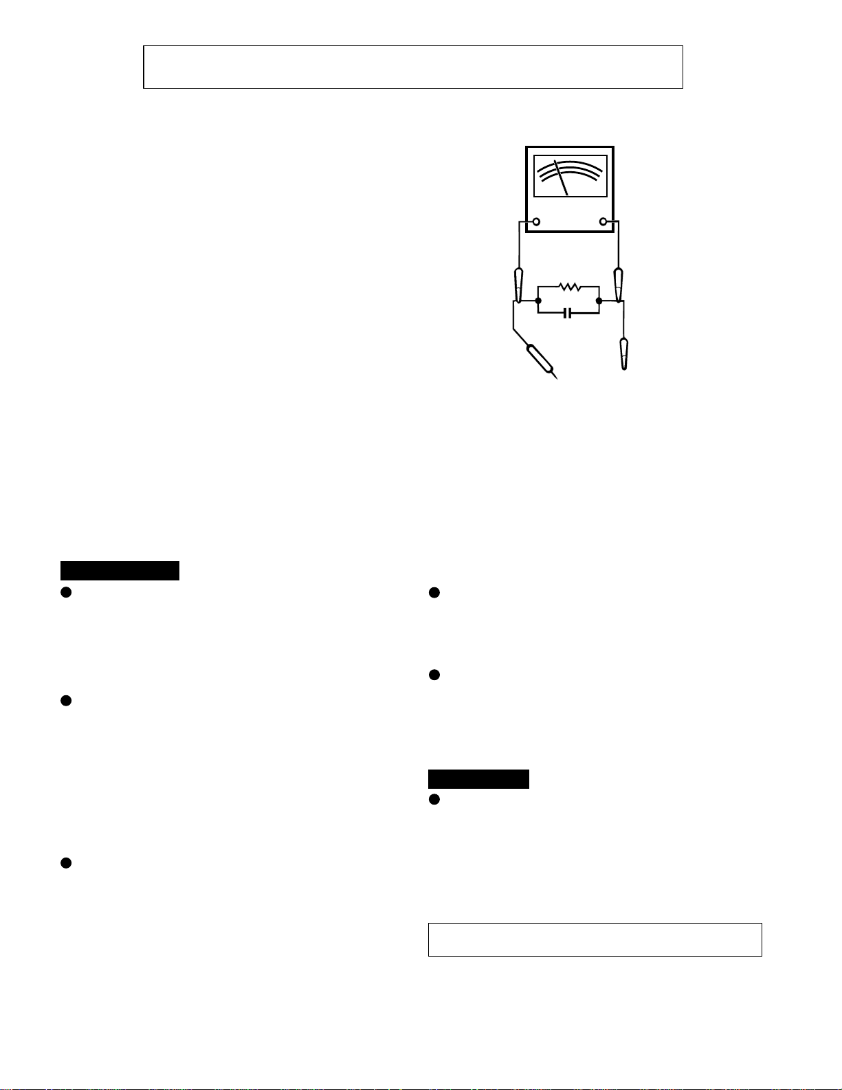
3. To be sure that no shock hazard exists, check for leakage
current in the following manner.
* Plug the AC line cord directly into a 120 volt AC outlet.
* Using two clip leads, connect a 1.5k ohm, 10 watt resistor
paralleled by a 0.15µF capacitor in series with all exposed
metal cabinet parts and a known earth ground, such as
conduit or electrical ground connected to earth ground.
* Use a VTVM or VOM with 1000 ohm per volt, or higher,
sensitivity to measure the AC voltage drop across the
resistor (See diagram).
* Connect the resistor connection to all exposed metal parts
having a return path to the chassis (antenna, metal cabinet,
screw heads, knobs and control shafts, escutcheon, etc.)
and measure the AC voltage drop across the resistor.
VTVM
AC SCALE
1.5k ohms
10W
0.15 µ F
TO EXPOSED
METAL PARTS
TEST PROBE
CONNECT TO
KNOWN EARTH
GROUND
All check must be repeated with the AC line cord plug connection
reversed.
Any reading of 0.3 volt RMS (this corresponds to 0.2 milliamp.
AC.) or more is excessive and indicates a potential shock
hazard which must be corrected before returning the audio
product to the owner.
SPECIFICATIONS
CD-C406/C
General
Power source: AC 120 V, 60 Hz
Power consumption: 40 W
Dimensions: Width; 10-5/8" (270 mm)
Weight: 9.2 lbs. (4.2 kg)
Amplifier section
Output power: 10 watts minimum RMS per channel into
(CD-C406) 8 ohms from 100 Hz to
Output power: MPO; 36 W (18 W + 18 W)
(CD-C406C) (10 % T.H.D.)
Output terminals: Speakers; 8 ohms
Tuner section
Frequency range: FM; 87.5 - 108 MHz
Height; 11-1/16" (280 mm)
Depth; 13-1/8" (332.5 mm)
20 kHz, 10 % total
harmonic distortion
RMS; 20 W (10 W + 10 W)
(10 % T.H.D.)
Headphones; 16 - 50 ohms
(recommended; 32 ohms)
AM; 530 - 1,720 kHz
Cassette deck section
Frequency response: 50 - 14,000 Hz (Normal tape)
Signal/noise ratio: 50 dB (TAPE 1, recording/playback)
55 dB (TAPE 2, playback)
Wow and flutter: 0.15 % (WRMS)
Compact disc player section
Type: 3-disc multi-play compact disc player
Signal readout: Non-contact, 3-beam semi-con-ductor
laser pickup
D/A Converter: 1-bit D/A converter
Frequency response: 20 - 20,000 Hz
Dynamic range: 90 dB (1 kHz)
CP-C406
Speaker section
Type: 2-way type [4" (10 cm) woofer and super
tweeter]
Maximum input power: 20 W
Impedance: 8 ohms
Dimensions: Width; 6-11/16" (170 mm)
Height; 11" (280 mm)
Depth; 5-15/16" (151 mm)
Weight: 3.1 lbs. (1.4 kg)/each
Specifications for this model are subject to change without prior
notice.
– 2 –
Page 3
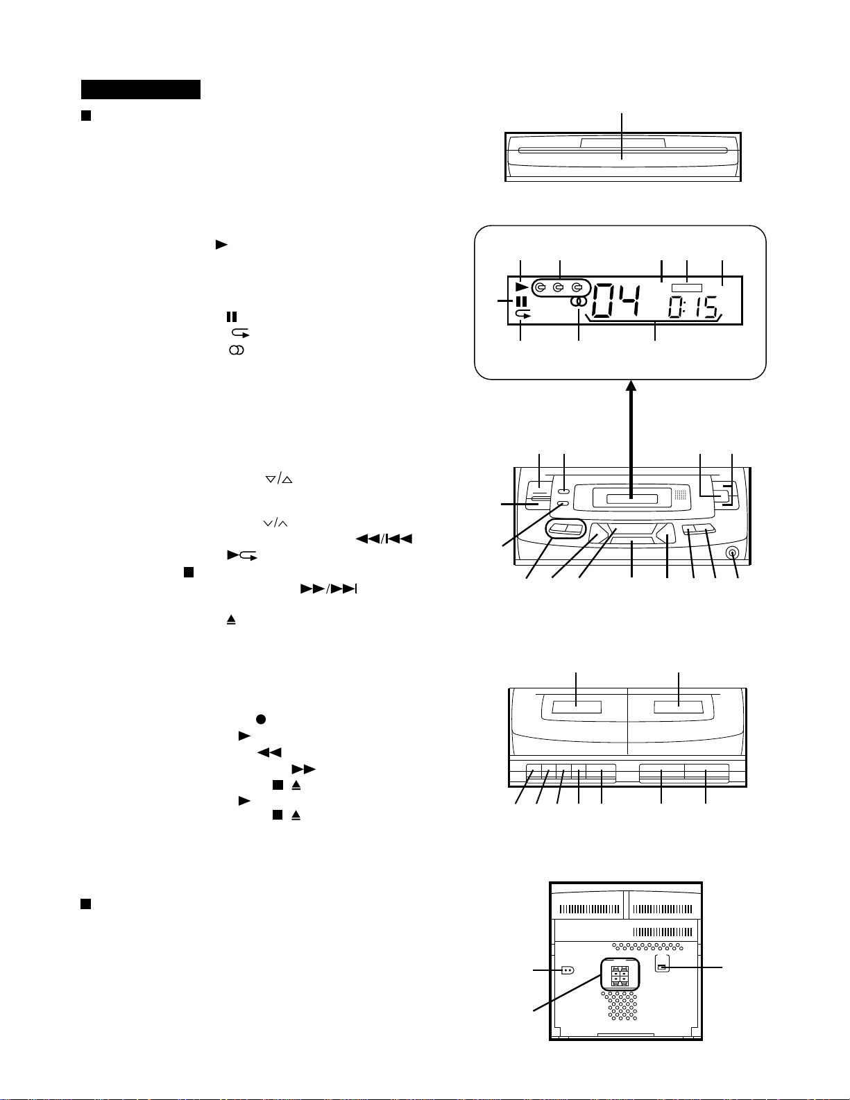
NAMES OF PARTS
CD-C406/C,CP-C406
CD-C406/C
Front Panel
1. Disc Tray
2. CD Play Indicator:
3. Disc Number Indicators
4. FM Stereo Mode Indicator: ST
5. Extra Bass Indicator: X-BASS
6. Memory Indicator
7. CD Pause Indicator:
8. CD Repeat Indicator:
9. FM Stereo Indicator:
10. Function/CD Track/CD Counter/Frequency/Preset
Channel/Volume Indicator
11. Power Switch
12. Memory Button
13. Extra Bass Button: X-BASS
14. Volume Up/Down Buttons:
15. Function Selector Button
16. Band Selector Button
17. Tuning Up/Down Buttons:
18. Track Down/Review/Preset Down Button:
19. Play/Repeat Button:
20. Stop Button:
21. Track Up/Cue/Preset Up Button:
22. Disc Skip Button
23. Open/Close Button:
24. Headphone Socket
1
23 4
123
5
X-BASS
ST
7
810
1112
9
13
15
16
17 18 19 20 21 2223 24
6
MEMORY
14
25. (TAPE 1) Cassette Compartment
26. (TAPE 2) Cassette Compartment
27. (TAPE 1) Record Button:
28. (TAPE 1) Play Button:
29. (TAPE 1) Rewind Button:
30. (TAPE 1) Fast Forward Button:
31. (TAPE 1) Stop/Eject Button:
32. (TAPE 2) Play Button:
33. (TAPE 2) Stop/Eject Button:
Rear Panel
1. AC Power Input Socket
2. Speaker Terminals
3. FM/AM Loop Aerial Socket
/
/
25
26
2728293031 32 33
1
2
3
– 3 –
Page 4
CD-C406/C,CP-C406
CP-C406
Speaker Section
4. Bass Reflex Duct
5. Speaker Wire
5
4
CD-C406/C
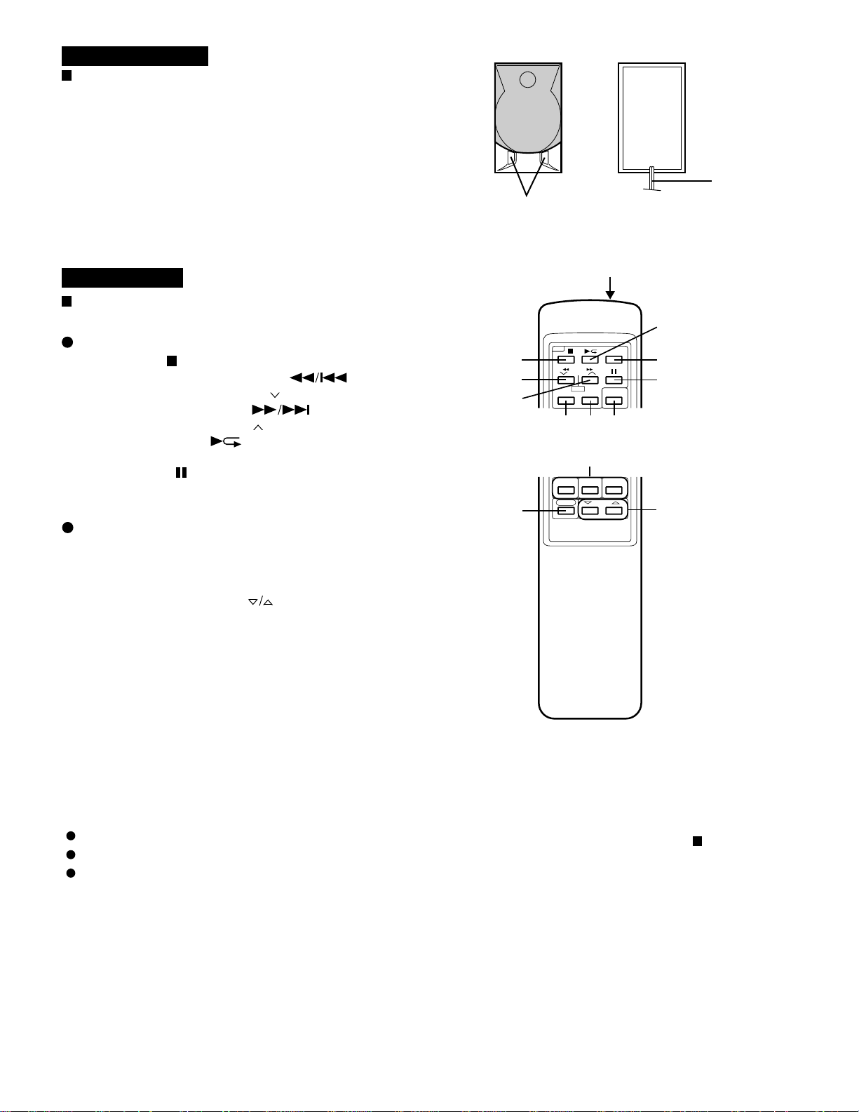
Remote Control
1. Remote Control Transmitter LED
CD Control section
2. Stop Button:
3. (CD) Track Down/Review Button:
(TUNER) Preset Down Button:
4. (CD) Track Up/Cue Button:
(TUNER) Preset Up Button:
5. Play/Repeat Button:
6. Disc Skip Button
7. Pause Button:
8. Memory Button
9. Clear Button
Common section
10. Extra Bass Button: X-BASS
11. Function Selector Buttons
12. Power Button
13. Volume Up/Down Buttons:
1
5
2
3
6
7
4
89
10
11
12 13
RESETTING THE MICROCOMPUTER
Reset the microcomputer by performing the
following procedure for the cases shown below:
To erase all of the stored memory contents, or
If the display does not function properly, or
The unit does not operate properly.
1
Press the POWER switch to turn the power off.
2
Press and hold down the POWER switch and button at the
same time. Hold them for at least 1 second.
3
Press the POWER switch to turn the power on.
– 4 –
Page 5
CD-C406/C,CP-C406
TAPE 1 TAPE 2
FUNCTION
STOP/EJECT PLAY STOP/EJECT
TAPE 1
FUNCTION
RECORD
STOP/EJECT
FUNCTION
BAND
TUNING
ST
FM STEREO
FM MONO
AM
VOLUME
VOLUME UP
VOLUME DOWN
X-BASS
Recording from CDs
Grabación de discos compactos
Tape playback
Reproducción de cintas
Radio operation
Funcionamiento de la radio
Precaución
Sound control
Control del sonido
"Cd" will appear
in the display.
Load the disc to
be recorded.
CD recording starts.
"Tape" will appear
in the display.
"Tuner" will appear
in the display.
Volume
Extra-BASS
"Cd" aparecerá
en el visualizador.
Introduzca el disco
que va a grabar.
La grabación de
CD empieza.
"Tape" aparecerá
en el visualizador.
"Tuner" aparecerá
en el visualizador.
El nivel de sonido en una posición de volumen
fijado depende de una combinación del
rendimiento de las altavoces, la posición y
muchos otros factores. Es aconsejable evitar un
aumento de volumen. Esto se produce, por
ejemplo, al conectar el aparato con el volumen
puesto en una posición alta. Evite continuar la
audición prolongada a altos
niveles de sonido.
En este aparato sólo pueden
reproducirse los discos que
tengan el logotipo mostrado.
Volumen
Bajos extras
X-BASS
VOLUME UP
VOLUME DOWN
X-BASS
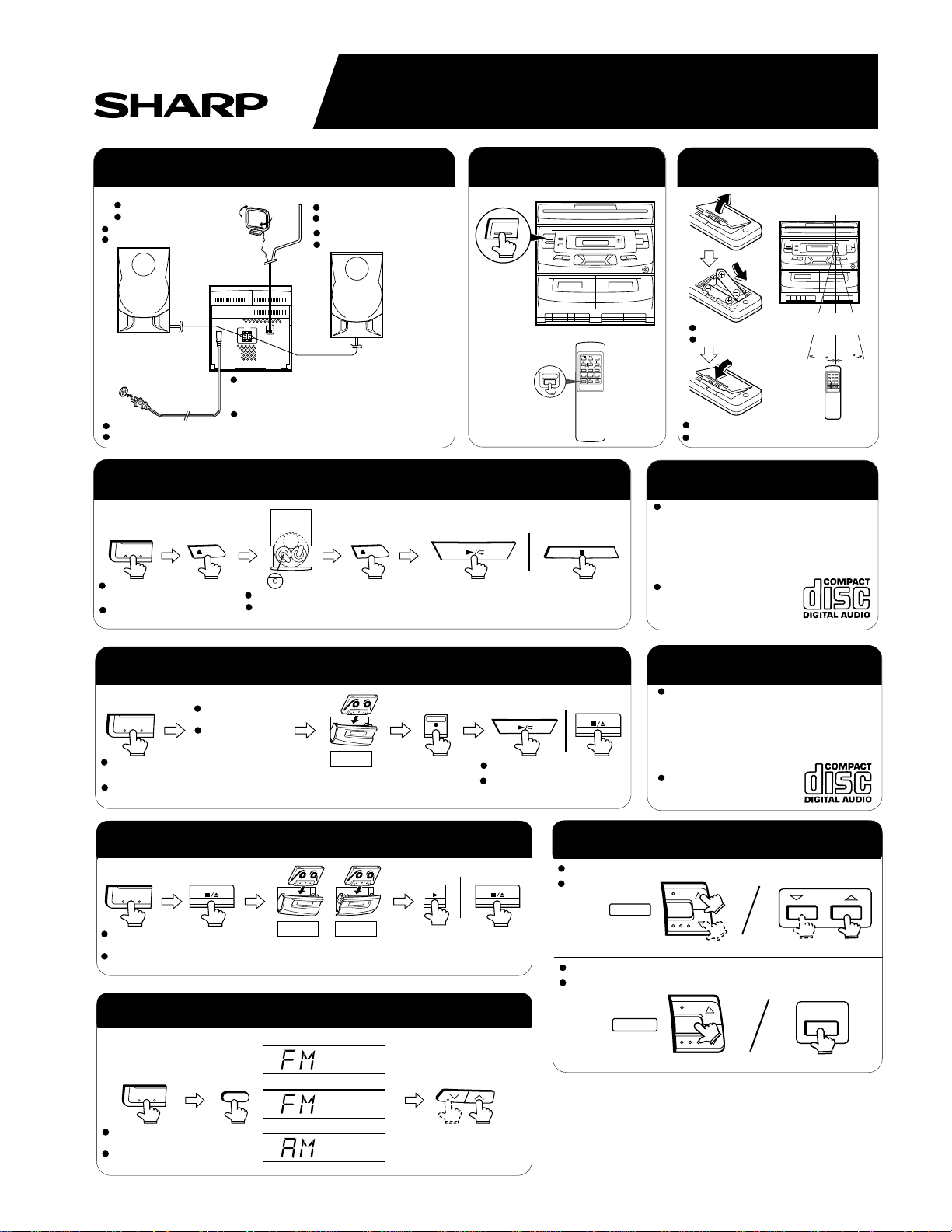
MINI COMPONENT SYSTEM
CD-C406
Quick-Guide
Guía rápida
Preparation for use
Preparación para su uso
15
15
FUNCTION
OPEN/
CLOSE
OPEN/
CLOSE
POWER
POWER
Turning the power on and off
Conexión y desconexión de la
alimentación
Remote control
Control remoto
CD playback
Reproducción de discos compactos
Precaution
FM Antenna
AM Loop Antenna
Right Speaker
Left Speaker
AC 120 V, 60 Hz
Connect the wire with the white line to the
minus (−) terminal and the plain wire to the
plus (+) terminal.
2 "AA" batteries
Batteries are not included.
Remote Sensor
8" - 20' (0.2m - 6m)
"Cd" will appear
in the display.
Label facing up
The sound level at a given volume setting
depends on a combination of speaker efficiency,
location and many other factors. It is advisable
to avoid exposure to high volume levels, which
occur while turning the unit on with the volume
control setting up high, or while continually
listening at high volume levels.
Only discs bearing the logo as
shown can be played in this
unit.
Antena de FM
Antena de cuadro de AM
Altavoz derecho
Altavoz izquierdo
120 V de CA, 60 Hz
Conecte el cable con la línea blanca al
terminal negativo (-) y el cable sin línea al
terminal positivo (+).
Dos pilas "AA"
Las pilas no están incluidas.
Sensor remote
0,2m - 6m
"Cd" aparecerá
en el visualizador.
Etiqueta hacia arriba
– 5 –
Page 6
CD-C406/C,CP-C406
DISASSEMBLY
Caution on Disassembly
Follow the below-mentioned notes when disassembling
the unit and reassembling it, to keep it safe and ensure
excellent performance:
1. Take cassette tape and compact disc out of the unit.
2. Be sure to remove the power supply plug from the wall
outlet before starting to disassemble the unit.
3. Take off nylon bands or wire holders where they need be
removed when disassembling the unit. After servicing
the unit, be sure to rearrange the leads where they were
before disassembling.
4. Take sufficient care on static electricity of integrated
circuits and other circuits when servicing.
CD-C406/C
STEP REMOVAL
1 Top Cabinet 1. Screw ..................... (A1) x4 6-1
2 Side Panel 1. Screw ..................... (B1) x6 6-1
(Left/right)
3 CD Player Unit/ 1. Turn on the power supply, 6-2
CD Tray Cover open the disc tray, take out
the CD cover, and close.
(Note 1)
2. Hook....................... (C1) x3
3. Hook....................... (C2) x2
4. Socket .................... (C3) x4
4 Back Board 1. Screw ..................... (D1) x3 6-2
5 Main PWB/ 1. Screw ..................... (E1) x10 7-1
Display PWB 2. Hook ....................... (E2) x2
3. Socket .................... (E3) x6
6 Front Panel 1. Screw ..................... (F1) x4 7-1
2. Hook....................... (F2) x3
7 Tape Mechanism 1. Open the cassette holder. 7-2
2. Screw...................... (G1) x6
8 Turntable 1. Screw ..................... (H1) x1 7-3
2. Cover ..................... (H2) x1
9 Disc Tray 1. Screw ..................... (J1) x2 7-3
2. Guide ..................... (J2) x2
10 CD Changer 1. Screw ..................... (K1) x4 7-4
Mechanism
11 CD Mechanism 1. Screw ..................... (L1) x1 7-4
Note 1:
How to open the change manually. (Fig. 6-3)
1. Insert the tip of fine screwdriver into the hole of CD player
base, and press down the worm wheel <A>.
2. Then, turn fully the lock lever in the arrow direction through
the hole on the loading chassis bottom in this state.
After that, push forward the CD player base.
PROCEDURE
FIGURE
(B1)x1
ø3x12mm
Side Panel
(Right)
CD Player Unit
Back Board
(D1)x1
ø3x8mm
CD-C406/C
(A1)x2
ø3x12mm
Hook
(B1)x2
ø3x12mm
(D1)x2
ø3x8mm
Push
(B1)x2
ø3x12mm
Hook
(C2)x1
Driver
Top Cabinet
Figure 6-1
CD Tray Cover
Figure 6-2
Hook
(B1)x1
ø3x12mm
(C3)x4
< A >
Hook
(C1)x3
(A1)x2
ø3x12mm
Side Panel
(Left)
Hook
(C2)x1
Driver
Push
CP-C406
STEP REMOVAL
1 Speaker 1. Front panel .............(A1) x1 7-5
2. Screw......................(A2) x4 7-6
PROCEDURE
FIGURE
– 6 –
LOCK
LEVER
Figure 6-3
Page 7
CD-C406/C,CP-C406
Screw
Driver
Driver should be pried
away from Speaker Box.
Direction of handle
Front Panel
(A1) x1
Speaker Box
(E3)x3
(E3)x1
(E1)x2
ø3x10mm
(E3)x1
(E1)x8
ø3x10mm
Hook
(F2)x3
Front Panel
Figure 7-1
Hook
(E2)x2
(E3)x1
(F1)x2
ø3x10mm
Front Panel
Display PWB
Main PWB
( K1 ) x4
ø3 x14mm
( L1 ) x1
ø2.6 x10mm
Shift Lever
CD Changer
Mechanism
CD Player Base
CD Mechanism
Care when installing the CD changer mechanism.
Install the CD changer mechanism on the CD player base after
the shift lever has been set in the highest position.
Figure 7-4
CP-C406
(G1)x6
ø3x10mm
( J1 ) x1
ø3 x10mm
( J2 ) x1
( H2 ) x1
Figure 7-2
( H1 ) x1
ø3 x10mm
Open
Cassette
Holder
(Left/Right)
Tape Mechanism
Turntable
Disc Tray
Super Tweeter
Woofer
(A2) x2
ø4x12mm
Figure 7-5
Speaker Box
CD Player Unit
( J2 ) x1
Figure 7-3
( J1 ) x1
ø3 x10mm
Figure 7-6
– 7 –
Page 8
CD-C406/C,CP-C406
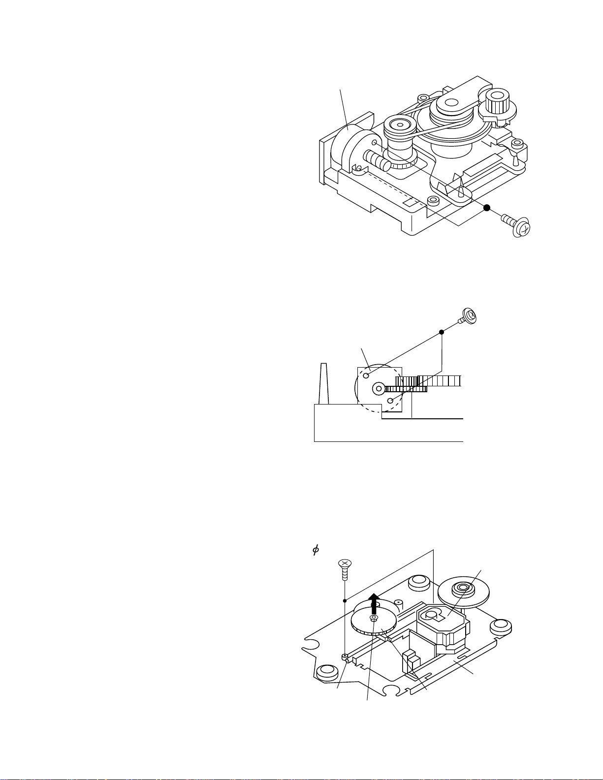
REMOVING AND REINSTALLING THE MAIN PARTS
CD MECHANISM SECTION
Perform steps 1, 2, 3, 13 and 14 of the disassembly method
to remove the CD mechanism.
How to remove the loading motor
(See Fig. 8-1)
1. Remove the screws (A1) x 2 pcs., to remove the loading
motor.
How to remove the turntable up/down motor
(See Fig. 8-2)
1. Remove the screws (B1) x 2 pcs., to remove the turntable
up/down motor.
Loading Motor
Turntable
Up/Down Motor
( A1 ) x2
ø2 x5mm
Figure 8-1
( B1 ) x2
ø2 x5mm
How to remove the pickup (See Fig. 8-3)
1. Remove the screws (C1) x 2 pcs., to remove the shaft (C2).
2. Remove the stop washer (C3) x 1 pc., to remove the gear
(C4).
3. Remove the pickup.
( C1 ) x2
2.6 x6mm
( C2 ) x1
( C3 ) x1
Figure 8-2
Pickup
CD Mechanism
( C4 ) x1
Figure 8-3
– 8 –
Page 9
ADJUSTMENT
L303
R319
T331
T301
L301
L302
CNP301
AM LOOP ANTENNA
T351
T333
IC351
IC301
FM RF
AM TRAKING fL
VCO
AM IF
FM IF
VR351
FM BAND
COVERAGE
FM DET.
AM BAND
COVERAGE fL
T352
MAIN PWB
1
13
21
C360
C364
TP303
TP302
TP301
+
MECHANISM SECTION
• Driving Force Check
Torque Meter
Play: TW-2412 Tape 1: Over 50 g
• Torque Check
Torque Meter
Tape 1
Play: TW-2111 30 to 60 g. cm 30 to 60 g.cm
Fast forward: TW-2231 — 80 to 135 g.cm
Rewind: TW-2231 — 80 to 135 g.cm
• Tape Speed
Test Tape
Normal MTT-111 Volume in 3,000 ± Speaker
speed motor 30 Hz terminal
Adjusting
Point
TUNER SECTION
fL: Low-range frequency
fH: High-renge frequency
• AM IF/RF
Signal generator: 400 Hz, 30%, AM modulated
Test Stage
IF 450 kHz 1,720 kHz T351 *1
Band — 530 kHz (fL): T333 *2
Coverage 1.1 ± 0.1 V
Tracking 990 kHz 990 kHz (fL): T331 *1
*1. Input: Antenna (CNP301), Output: TP302
*2. Input: Antenna (CNP301), Output: TP301
Frequency Frequency
Display
TAPE MECHANISM
Volume in motor
Specified Value
Tape 2: Over 100 g
Specified Value
Specified
Value
Setting/
Adjusting
Parts
Tape 2
Instrument
Connection
(Load
resistance:
8 ohms)
Instrument
Connection
CD-C406/C,CP-C406
• FM RF
Signal generator: 1 kHz, 75 kHz dev., FM modulated
Test Stage
Frequency
Frequency
Display
Serring/
Adjusting
Point
Band — 87.50 MHz L303(fL): *1
Coverage 3.4 V ± 50 mV
RF 98.00 MHz 98.00 MHz L302 *2
(10-30 dB)
*1. Input: Antenna (CNP301), Output: TP301
*2. Input: Antenna (CNP301), Output: Speaker terminal
• Detection
Signal generator: 10.7 MHz, FM sweep generator
Test
Frequency
Stage
Detection 10.7 MHz 98.00 MHz T352 Input: Pin 1 of
IF 10.7 MHz 98.00 MHz T301(Turn Input: Pin 1 of
Frequency
Display
Adjusting
Parts
the core of IC301
transformer Output: TP302
T352 fully
counterclookwise.)
• VCO Frequency
Frequency
Frequency
Display
98.00 MHz 98.00 MHz VR351* Pin 13, Pin 21
(60 dB) and ground
Adjusting
Parts
* Adjust for 76 kHz ± 200 Hz.
Notes:
After preparing the test circuit shown in Fig 9-2, connect the
Pin 13 , Pin 21 and ground of the IC351 with test circuit, and
measure the Value.
At this time, apply a standard unmodulated signal input and
adjust the VCO.
Pin 13 of IC351
G
Pin 21 of IC351
FET : 2SK19 or 2SK54
D
S
10 kohm
Figure 9-2
Instrument
Connection
Instrument
Connection
IC301
Output: TP302
Instrument
Connection
of IC351
TO FREQUENCY
COUNTER
Figure 9-1 ADJUSTMENT POINTS
– 9 –
Page 10
CD-C406/C,CP-C406
CD SECTION
Since this CD system incorporates the following automatic
adjustment function, when the pickup is replaced, it is not
necessary to readjust it.
Since this CD unit does not need adjustment, the combination
of PWB and laser pickup unit is not restricted.
• Automatic adjustment item
1. Focus offset (Fig. 10-1)
2. Tracking offset (Fig. 10-2)
3. E/F balance (tracking error balance) (Fig. 10-3)
4. RF level AGC function (HF level: constant)
5. RF level automatic follow-up of the tracking gain
This automatic adjustment is performed each time a disc is
changed.
Therefore, each disc is played back using the optimal settings.
0.1s
0.50 V
IC1 20 FE
FOCUS
OFF-SET
ADJUST
0.1s
0.50 V
IC1 7 TE
Figure 10-1
TRACKING
OFF-SET
ADJUST
1
2
CD TEST MODE
When the PLAY and POWER keys are
pressed at the same time in OFF MODE, the
set will enter CD TEST MODE
IL is not
performed.
↓
"CD TEST" of LCD will light up.
↓
The pickup can be moved by using the ( ) or
( ) key.
→
↓
LASER ON
↓
FOCUS SERVO ON
↓
TRACKING ON THE STOP
SERVO OFF PLAY
Display "CD 01 0:00"
↓
TRACKING ON THE STOP
SERVO OFF PLAY
↓
STOP "CD TEST" will display
Press PLAY key
Press PLAY key
Press PLAY key
Press PLAY key
Press PLAY key
10ms
0.50 V
IC1 20 FE
10ms
0.50 V
IC1 7 TE
200 ms
1V/diV
IC 1 15
TO
200 ms
1V/diV
IC 1 7
TE
Figure 10-2
Figure 10-3
Enlarged
View
TRACKING
OFF-SET
ADJUST
1
2
TRACKING/
ERROR
BARANCE
1
ADJUST
2
Cancel method: POWER OFF
LCD display: After the PLAY or APMS MEMORY ke y has been
pressed, the track No. and time only will appear
(valid). The other items are optional.
Note: The pickup can be slid using the or key only
while in the stop mode.
ALL CLEAR AND RE-START FUNCTION
When the STOP and POWER keys are pressed to turn on the
power, the entire internal memory will be cleared and the
mechanism will run from address 0.
All of the tuner presets, APMS, TOC and disc numbers which
were last stored in memory will be cleared, and the tuner,
changer mechanism and all of the other items will be initialized.
– 10 –
Page 11
NOTES ON SCHEMATIC DIAGRAM
• Resistor:
To differentiate the units of resistors, such symbol as K and
M are used: the symbol K means 1000 ohm and the symbol
M means 1000 kohm and the resistor without any symbol is
ohm-type resistor. Besides, the one with “Fusible” is a fuse
type.
• Capacitor:
To indicate the unit of capacitor, a symbol P is used: this
symbol P means micro-micro-farad and the unit of the
capacitor without such a symbol is microfarad. As to
electrolytic capacitor, the expression “capacitance/withstand
voltage” is used.
(CH), (TH), (RH), (UJ): Temperature compensation
(ML): Mylar type
(P.P.): Polypropylene type
• Schematic diagram and Wiring Side of P.W.Board for this
model are subject to change for improvement without prior
notice.
CD-C406/C,CP-C406
• The indicated voltage in each section is the one measured
by Digital Multimeter between such a section and the chassis with no signal given.
1. In the tuner section,
( ) indicates AM
< > indicates FM stereo
2. In the main section, a tape is being played back.
3. In the deck section, a tape is being played back.
( ) indicates the record state.
4. In the power section, a tape is being played back.
5. In the CD section, the CD is stopped.
• Parts marked with “ ” ( ) are important for
maintaining the safety of the set. Be sure to replace these
parts with specified ones for maintaining the safety and
performance of the set.
REF. NO DESCRIPTION POSITION POSITION
SW1 OPEN/CLOSE ON—OFF
SW2 MWCHA UP ON—OFF
SW3 DISC NUMBER ON—OFF
SW4 PICKUP IN ON—OFF
SW605 TAPE 1 MAIN ON—OFF
SW606 TAPE 2 MAIN ON—OFF
SW607 REC. ON—OFF
SW701 RANDOM/DEMO ON—OFF
SW702 VOLUME DOWN ON—OFF
SW703 X-BASS ON—OFF
SW704 VOLUME UP ON—OFF
SW705 OPEN/CLOSE ON—OFF
SW706 DISC SKIP ON—OFF
SW709 REC./PAUSE ON—OFF
SW710 UP ON—OFF
FRONT
VIEW
FRONT
VIEW
REF. NO DESCRIPTION
SW711 STOP ON—OFF
SW712 PLAY ON—OFF
SW713 DOWN ON—OFF
SW714 TUNING UP ON—OFF
SW715 TUNING DOWN ON—OFF
SW717 POWER ON—OFF
SW718 CLOCK ON—OFF
SW719 TIMER/SLEEP ON—OFF
SW721 MEMORY/SET ON—OFF
SW722 CD ON—OFF
SW723 TUNER ON—OFF
SW724 TAPE ON—OFF
SWM 3 FOOL PROOF ON—OFF
SWM 4 F.A.S. ON—OFF
SWM 5 CAM ON—OFF
FRONT VIEW
2SA1015 GR
2SB561 C
2SC2389 SS
2SC535 C
KRA102 M
KRA109 M
KRC102 M
E C B
(S)(G)(D)
(1) (2) (3)
KRC107 M
KTA1266 GR
KTA1273 Y
KTC3199 GR
KTC3203 Y
E C B
(D)(G)(S)
(3) (2) (1)
2SD2012 Y KDV147BKRC104 M
Figure 11 TYPES OF TRANSISTOR
– 11 –
KV1236Z23F
Page 12
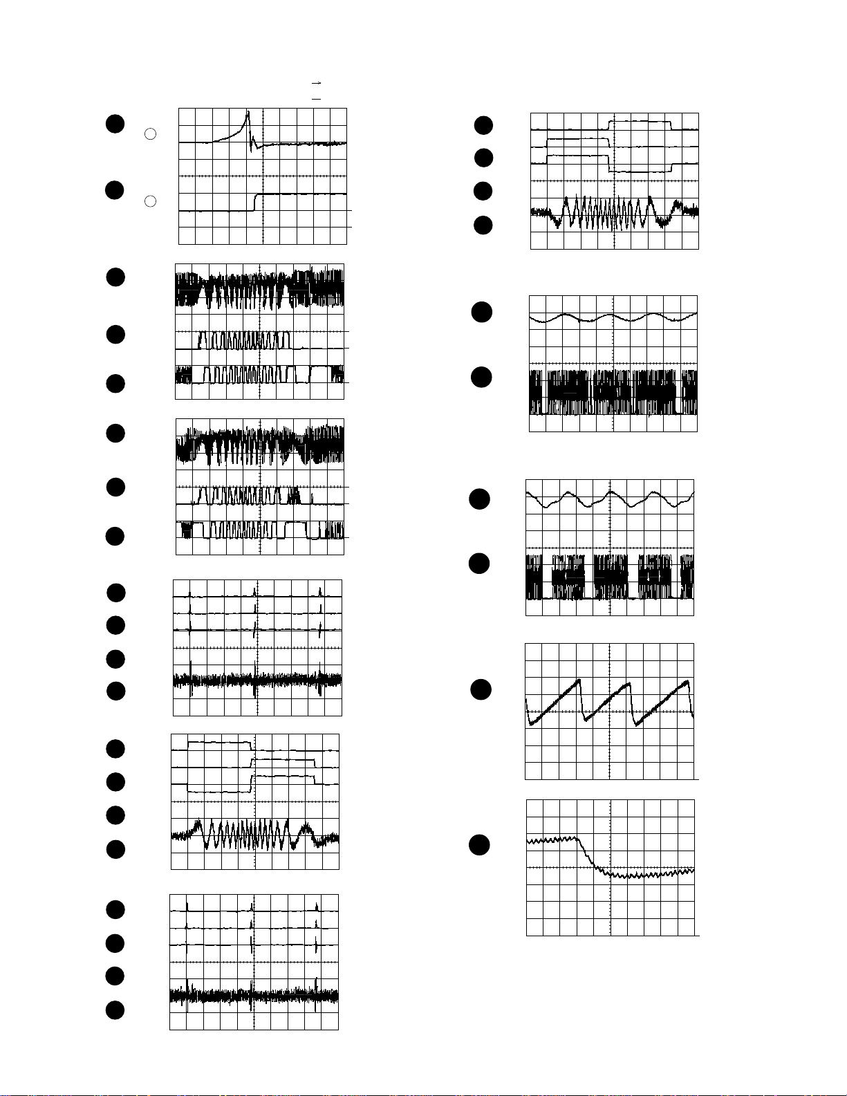
CD-C406/C,CP-C406
5ms
0.50 V
1
IC1 20 F.E
5ms
5.0 V
2
IC1 54 DRF
WAVEFORMS OF CD CIRCUIT
STOP PLAY
FOCUS SERCH
0.5ms
6
10.0 V
JP+
0.5ms
7
10.0 V
JP-
0.5ms
8
3
1
0.50 V
JP
0.5ms
9
1.00 V
TE
0.5ms
3
1.00 V
HF
0.5ms
4
5.0 V
HFL
0.5ms
5
5.0 V
TES
0.5ms
1.00 V
3
HF
0.5ms
4
5.0 V
HFL
0.5ms
5
5.0 V
TES
50ms
6
10.0 V
JP+
50ms
7
10.0 V
JP-
50ms
8
0.50 V
JP
50ms
9
1.00 V
TE
CUE
1
2
3
REVIEW
1
2
3
CUE
10
11
10
11
12
20ms
1.00 V
SPO
20ms
2.00 V
CLV+
50ms
1.00 V
SPO
50ms
2.00 V
CLV+
5s
100mV
SLD
PLAY
NORMAL DISC
TN0=01
PLAY
TCD-712 (140mm)
TN0=01
PLAY
TCD-712
0.5ms
10.0 V
6
JP+
0.5ms
10.0 V
7
JP-
0.5ms
0.50 V
8
JP
0.5ms
9
1.00 V
TE
50ms
10.0 V
6
JP+
50ms
10.0 V
7
JP50ms
8
0.50 V
JP
50ms
9
1.00 V
TE
REVIEW
12
0.5s
100mV
SLD
1
1
– 12 –
Page 13
1
2
3
4
6
7
13
12
24
253031
64
6
62
8
26
29 30 31 54 51 54
32
404344
49
50
15
16
27
10
12
20
61
9
45 44 23 11 43
53
58
24
28
373839
40
36
41
1
9
3
7
M
1
2
3
4
5
6
7
8
9
10
11
12
13
14
15
16
17
18
19
20
1
1
5
17
20
11
29
22 23
32
2
6
~
IC1
LA9241M
SERVO AMP.
RES. CQCK. COIN
SQOUT. RWC. WRQ
IC2
LC78623D
SERVO/SIGNAL
CONTROL
IC5
M56748FP
SL+, SL–, DRF
XIN XOUT
+B
4.3V
FOCUS COIL
TRACKING COIL
M
M
PICKUP UNIT
XL1
16.93MHz
FOCUS/
DRIVER
SPIN/SLIDE/
TRACKING/
PICKUP IN
SW4
Q1
M4
SLIDE
MOTOR
M3
SPIN
MOTOR
+5V
~~
~
~
DEF, CLK, CL, DAT, CE, DRF
~
+B
4.3V
IC91
TA7291S
Q91
Q93
SW2
M3
LOADING/
UP/DOWN
MOTOR
CHANGER MECHA
+B
5V
+B
4.3V
D81
DISC UP SW
CNS10
PU-IN SW
DISC NO. SENSOR
DRF
WRC
RES
RWC
SLM+
SLM–
LOADING H/L
CQCK
SQ OUT
CO IN
12V MECHA
GND
R-CH OUT
AUDIO GND
L-CH OUT
(OPEN)
TO MAIN
SECTION
~
+B
4.3V
5V CDSVO
MECHA UP SW
IC91: MOTOR DRIVER
LASER
POWER
CONTROL
ALPC
SW3
DISC No. SW
SW1
OPEN/CLOSE SW
PL1
PLUNGER
PLUNGER
DRIVER
SW
CD-C406/C,CP-C406
Figure 13 BLOCK DIAGRAM (1/3)
– 13 –
Page 14
CD-C406/C,CP-C406
4
O
FM FRONT END
TA7358AP
MIX
RF
4
3
1
FM
ANTENNA
FM ANTENNA
AM LOOP
ANTENNA
3
2
1
CNP301
FM AM ANT.
TERMINAL
BF301
2
13
VD301
FM IN
L302 T301 L303
FM RF
AM ANT. AM OSC.
T331 T333
CD
SECTION
IC301
VD331-2VD331-1
6
57
FM IF
B.A
OSC
89
FM
OSC.
VD302
Q302
CF302
FM +B
RF AMP
FM IF IN
10.7MHz
8
D381
+B5
AM IF
T351
CF351
AM MIX
OUT
1
3
IC351
LA1805
FM IF DET. /FM MPX. /AM IF
67
AM +B
AM OSC
AM RF IN
X381
4.5MHz
VT
1
7
FM
Q381
SWITCHING
T352
AM IF
IN
5
FM DET
DET OUT
FM IN
IC381
LC72131
PLL
+B5
FM DET
VCC
20 21 11
L OUT
R OUT
MPX IN
STEREO
MONO/STST
AM IN
ST
101115162220
4
3
6
5
DI
CL
CE
DO
SWITCHING
FM/AM
9
10
131524 17 162322
VDD
21
Q352
L
R
VR351
FM VCO
17
FM +B
VOLTAGE
REGULATOR
ZD381
MM1
TAPE
MOTOR
TAPE2
P.B. HEAD
L-CH
R-CH
TAPE1
REC/P. B. HEAD
L-CH
R-CH
ERASE
HEAD
M
D202D201
+B4
SW606
T2 MAIN
SW605
T1 MAIN
SW608
T1 PLAY
REC. /P. B. AMP.
L NF
Q207~
Q209
BIAS OSC
Q212
L203
24
23
3
22
6
16
12
Nor/
CrO
1
2
9
AN7345K
15
2
IC201
P. B
ALC
L
R
1110
13
4
21
19
7
18
8
17
ALC CUT
Q201
Q202
REC
SWITCHING
Q201
Q206
PB
~
T1 L
T1 R
T2 L
T2 R
R NF
POP
REDUCE
L REC REC
R REC
SWITCHING
VCC
L OUT
R OUT
T1/T2
L REC IN
R REC IN
CLDICE
232425
16 33 14
LR
9
L
T
T
L
21
CD
R
28
L
19
T2 ON
T1 PLAY
T1/T2
+B5
Q210
REC MUTING
Q213
Q211
SWITCHING
REC
REC
SW607
+B4
TUNER
TAPE
R
30
L
17
R
32
Figure 14 BLOCK DIAGRAM (2/3)
– 14 –
Page 15
KEY MATRIX
CE
SW702 ~ SW716
CD-C406/C,CP-C406
LCD701
COM 0 ~
COM 3
S0 ~ S20
21
22
25
~~
LCD BIAS
~
25 28
29
~~
32
34
KEY IN
37
DO
63
DI
65
CE
66
CL
64
INITIAL1
INITIAL2
IX0217AW
MICROCOMPUTOR
21
COM OUT SEG OUT
IC701
SYSTEM
~~
~
T1/T2
T2 ON
T1 PLAY
POWER CONT.
24
1
535261 62 67 40 51
53 53
VDD
POWER CONT.
1
~
80
69
9
RESET
SYSTEM STOP
REMOCON
59
XL701
4.19MHz
68
13
38
58
Q701
Q702
Q703
POWER FAIL
DETECTOR
RX701
REMOCON
D703
+B6
GRAPHIC EQUALIZER
CL
DI
5
98
AUDIO PROCESSOR
16 33 14 35 56 63 50 26 27 12 37 11 38 10 39
LR
LR
TO CD SECTION
TO CD SECTION
6
7
IC431
LC75394E
GRAPHIC EQUALIZER
V REF
+B4
+12V
+B5
+12V
+B6(5V)
L VREF
(MECHA)
(ANALOG)
5
R VREF
4
A VSS
VSS
Q925
Q926
VOLTAGE
REGULATOR
IC922
VOLTAGE
REGULATOR
IC921
3
X- BASS
2
1
VOLUME
VOLTAGE
REGULATOR
Q924
VDD
4847464544434241402324
OUT
8
5
L
55
R
7
5
+B5
Q641
VOLTAGE
REGULATOR
IC601
LA4282
POWER AMP.
2
L-IN
5
R-IN
1
NF
6
3
P-CONT
D905 ~ D908
4
GND
9
L-OUT
11
R-OUT
7
10
12
VCC
GND
33V
D901 ~ D904
SPEAKER SWITCH
T901
POWER
TRANSFORMER
T.F
J601
HEADPHONES
120V
SO601
SPEAKER
TERMINAL
AC SOCKET
SO901
AC POWER
SUPPLY CORD
AC 120V 60Hz
Figure 15 BLOCK DIAGRAM (3/3)
– 15 –
Page 16
CD-C406/C,CP-C406
0.01
C1
R1
1K
C2
47/10
Q1
KTA1266 GR
C25
0.01
LA9241M
SERVO AMP.
C3
0.1/50
R2
100K
C4
0.001
R4
2.2K
C6 0.033
R5
6.8K
R6
100
R7
1K
C9
0.047
R9
(ML)
27K
R11
3.3K
C75
100P
R281KR29
R39
22K
R40
22K
C11
0.1
(ML)
3V
C5
0.033
3.6V1.3V
R8
12K
C10
180P
330/10
IC1
(ML)
C8
0.068
1K
C44
15K
C7
0.1/50
(ML)
+B
C24
1/50
R3
(ML)
R12
15K
R43
12
R13
33K
VCC1
FIN2
1
REF
FIN1
2
REF
E
3
F
4
TB
5
TE-
6
TE
7
TESI
8
9
SCI
TH
10
11
12
TD-
TD
13
JP
14
TO
15
FD
16
C13
0.1
(ML)
1
2
3
4
5
6
7
8
9
10
11
12
13
14
15
16
17
18
+B
R45 1K
4.7K
R32
C21
1/50
+B
56K
C45
4.7/25
C34
0.033
(ML)
R36
47K
C32
27P
R35
470
C50
0.1
(ML)
R34
1K
C31
0.0027
R46 1K
R47 1K
R38
33K
R37
47K
D2
1SS133
+5V
C53
220P
LUG1
C40
0.33/50
C39
C38
0.01
C37
C35
58
FE1
C15
VR
+
–
+
–
–
+
+
–
+
–
+
–
REF
REF
–
REF
SPI
252627
24
0.0047
220/6.3
56
57
REF1
DEF
HFL
DRF
VCC
REF
FSTA
S.Q.R
+
–
+
SPG
SP–
R21
56K
R22
R20 10K
6.8K
R23
1.2K
C17
0.47/50
0.1/50
VCC2
EFBAL
FOSTA
TOSTA
2FREQ
LASER
FSTA
8/12CM
SLOF
REF
JP
C16
0.001
55
FSS
DRF
+
–
+
–
JPCLO
REF
SLEO
SPO
28
C19
47/10
R25
CV–
CV+
JP–
JP+
OR
1.2K
49
DEF
CL
CE
CLK
DAT
FSC
CE
REF
CL
LATOH
REF
RF
RFSM
CV+
CV–
SLOF
SLOF
SLOF
SLOF
+
–
TES
+
–
REF
SL–
SLD
SL+
29
30 31
C18
1/50
10K
R24
18K
R30
R41
48
TBC
47
46
DGND
45
SLI
44
––+
C33
0.001
SLC
43
R33
5.6K
RFS–
42
+
C30
2.2P
41
TP1
40
39
38
HFL
37
36
TOFF
35
TGL
34
JP+
33
JP–
32
R27
220K
C20
0.0033
R26
220K
R10
82K
50
54
515253
0.47/50
560
R42
64
63
62
LDS
LDO
–
+
RF
–
+
–
–
+
+
REF
–
+
VCR
REF
–
+
+
REF
–
REF
REF
+
–
+
GEN
REF
–
TO
REF
GEN
+
–
REF
REF
+
+
–
–
FA
FA–
FD-
19
17
18
R14
10K
R15
47K
IC5
M56748FP
596061
LF2
PHI
BHI
REF
FE1
REF
VCR
VCR
–
+
VCR
+
–
+
TGL1
–
GL
THDL
THD
JP
FSC
FOSTA
GEN
REF
+
–
+
–
REF
AGND
SP
FE
FE–
23
22
20
21
C12
330P
R17
82K
C14
0.01
R16
1.5K
R19
39K
36
35
34
33
32
31
30
29
28
27
26
25
R31
24
10K
23
22
FOCUS/TRACKING/
SPIN/SLIDE DRIVER
21
20
19
+B
A
CNS1B
K
B
1
2
E
3
A
B
4
F
5
CNS1A
1
2
3
4
5
CNP1
1
2
3
4
5
C
PICK UP UNIT
K
1
E
2
A
3
B
4
D
F
5
1
2
3
4
5
6
7
8
1/16
VR1A
1M
2200P
1M
2200P
TR+
FO+
FOTR-
ACTUATOR
E
CNS2B
CNS2A
CNP2
1
1
1
TR_
2
2
2
TR+
3
3
3
FO+
4
4
4
FO_
GND
F
CD MOTOR
PWB-B
5
5
5
PD
6
6
6
VR
7
7
7
LD
8
8
8
CNS3B
CNS3A
M1
SPIN
M
MOTOR
G
M2
SLIDE
MOTOR
SW4
PU-IN
M
6
5
4
3
2
1
CNP3
SP+
6
6
SP_
5
5
SL+
4
4
SL_
3
3
PU-IN
2
2
1
1
H
• NOTES ON SCHEMATIC DIAGRAM can be found on page 11.
1
23456
Figure 16 SCHEMATIC DIAGRAM (1/9)
– 16 –
R54
1K
PUIN
SL–
SL+
1324
DRF
TO
Page 17

CD-C406/C,CP-C406
1K
1K
1K
33
V
SL+
3
C53
220P
LUG1
R77 1K
DRF
COIN
SQOUT
RWC
CQCK
4 56789
P24 5 - H
TO DISPLAY PWB
C22
3.3M
C41
0.047
(ML)
C42
0.047
0.022
R18
C59
(ML)
(ML)
R57
27K
R56
1.2K
0.01
64
63
TEST1
DEF1
1
TA1
2
PDO
3
R58
VVSS
680
4
ISET
5
VVDD
6
FR
7
VSS
8
EFMO
9
EFMIN
10
TEST2
11
CLV+
12
CLV_
13
V/P
14
HLF
15
TES
COMMAND
16
TOFF
17
CD-LD M+
LOADING
MOTOR DRIVER
62
/CS
TEST5
CONTROL
DIGITAL
SERVO
SERVO
TGL
18
R99
3.9
SLICE
LEVEL
CLV
+B
+B
1234
C91
47/16
R78 1K
+B
_
WRQ
DSP RES
DISC NO
10 11 35
R60
1K
58596061
4M
16M
/RES
TEST11
VCO
CLOCK
OSC
CONTROL
EFM DEMODULATE
JP_
JP+
PCK
FSEQ
19
2021222324
+B
C52
100/10
IC91
TA7291S
5
6
R97
12K
M_GND
56
55
57
COIN
/CQCK
SQOUT
µ-COM
INTERFACE
2KX8
RAM
ERROR
COERECT
FLAG
CONTROL
SYNC-DETECT
EXTERNAL
CONT1
VDD
R86 1K
7
89
R98
5.6K
C73
100P
MOTOR GND
54
RWC
WRQ
OUTPUT
CONT4
CONT3
CONT2
26
27
25
R88 1K
R87 1K
CD-LD M–
R92
10K
C54
100P
50
515253
SFSY
FSX
SBCK
SUB-CODE
GENERATOR
EMPH
CONT5
29
28
MECHA UP
OPEN/CLOSE
R89 1K
R90 1K
L2
27µH
3
0V
1
0V
R91
10K
C55
100P
49
PW
X-TAL
4FS
DIGITAL
C2F
DOUT
30
31
11.2V
2
Q93
KRC102 M
L3
47µH
C57
100P
FILTER
DIGITAL
OUT
+B
R93
4.7
11.3V
R95
2.2K
32
C56
MUTER
TEST3
R96
17
100P
EFLG
SBSY
XVSS
XIN
XOUT
XVDD
RVDD
RCHO
RVSS
1BIT
DAC
LVSS
LCHO
LVDD
MUTEL
NC
TEST4
+12V
D_GND
Q91
KTA1271 Y
0V
10K
11.2V
OPEN CLOSE
D_GND
+B
+B
48
47
46
45
44
C71
43
330P
42
41
10/16
40
39
38
10/16
37
36
35
C43
34
100/10
33
IC2
LC78623D
SERVO/SIGNAL
CONTROL
R82
100
0.82µH
C51
0.022
D91
1SS133
CNP4
SOL
GND(M)
M+
M–
GND(D)
DISC NO.
GND(D)
MECHA UP
GND(D)
MAIN PWB-A(1/4)
XL1
16.9344MHz
C68
R74
4.7K
C67
R73
4.7K
C72
100P
L1
+4.3V
+B
AUDIO GND
CNS4
1
1
2
2
3
3
4
4
5
5
6
6
7
7
8
8
9
9
10
10
1
2
CNS5
+B
R76
C70
1K
220P
C69
R75
220P
1K
C58
+B
+B
D81
1SS133
C74
100P
CD SIGNAL
MOTOR
PWB-C
BIM05
1
SOLM2
LOCK
2
+
3
M
4
–
5
SW1
6
OPEN
CLOSE
SW2
MECH UP
SW3
DISC NO
220P
M3
UP/DOWN
LOADING
12
CD_R
13
CD A GND
14
CD_L
+12V DRIVER
15
19
+5V (uCOM)
D_GND
17
TO DISPLAY PWB
19
+5V (SERVO)
P18 1 - D,1 - E
TO MAIN SECTION
• The numbers 1 to 12 are waveform numbers shown in page 12.
7
8 9 10 11 12
Figure 17 SCHEMATIC DIAGRAM (2/9)
– 17 –
Page 18

CD-C406/C,CP-C406
3
3
E
K
6
/
6
A
B
C
D
P17 12 - D
TO CD SECTION
P21 12 - F
TO DECK SECTION
P17 12 - D
TO CD SECTION
E
TO DISPLAY
F
P24 5 - A
PWB
CD_L
14
CD_A_GND
13
CD_R
12
+5V(µ-COM)
19
GND(D)
17
POWER
20
+12V(MECHA)
34
+12V(SERVO)
15
POWER_CONT
22
+5V(µ-COM)
19
GND(µ-COM)
37
GND (MECHA)
38
FM SIGNAL
PLAYBACK SIGNAL
RECORD SIGNAL
CD SIGNAL
CD +B
+B
+B
C435
0.047
R460 1K
R461 1K
R462 1K
C436
0.047
(ML)
C433
0.047
C431
0.047
C432
0.047
C434
0.047
(ML)
(ML)
(ML)
(ML)
(ML)
R452
1K
C439
22/16
C440
22/16
R447
3.3K
17
18
19
20
21
22
23
24
25
26
27
28
29
30
31
32
R448
3.3K
C482
2.2/50
C441
180P
L3
L2
L1
VSS
CL
DI
CE
VSS
AVSS
R1
R2
R3
C442
180P
+B
+B
R449
12K
C443
0.68/50
14
L SELO
13
LT IN
12
11
LF1C1
LF1C2
15
16
LI VIN 1
AUDIO PROCESSOR
RT IN
R SELO
RIN VIN 1
RF1C1
+B
36
C925
37
C444
0.68/50
C481
2.2/50
+B
0.022
+B
RF1C2
38
(ML)
Q925
KTA1271 Y
11.2V
10.6V
R922
2.2K
33
R451
R450
12K
1K
+B
34
35
+B
C445
(ML)
0.022
7
10
89
LF1C3
IC431
LC75394E
RF1C3
39
404142
C446
0.022
11.3V
R923
2.2K
2
Q926
3
0V
0V
1
6
43 44
AUDIO +B
MECHA +B
KRC102 M
4.2V
5
45 464748
10K
R924
CD +B
1234
LFS
LVref
LIN VIN 2
LT OUT
LVR IN
LTEST
LVR OUT
VDD
Vref
RVR OUT
RTEST
RVR IN
RT OUT
RIN VIN 2
RVref
RFS
+B
+B
(ML)
C922
0.022
C926
47/16
64
63
62
61
60
59
58
57
56
55
54
53
52
51
50
49
VOLTAGE
REGULATOR
Q924
2SD2012 Y
11.3V
12V
VOLTAG
C459
0.0027
C463
100P
C46
10/165
C475
100/10
C466
10/16
C464
100P
C460
0.0027
R935
150
C923
0.1
(ML)
17.6V
12V
+B
C4
100
C4
100/
G
+12V
36 35 39 33 32 35
P23 12 - E
TO TUNER
SECTION
26 27 28 17 31 30 17
P23 12 - F,
24 3 - A
TO TUNER
SECTION,
DISPLAY
PWB
GDN(D)
CE
DI
CL
LOUT
ROUT
H
• NOTES ON SCHEMATIC DIAGRAM can be found on page 11.
1
23456
Figure 18 SCHEMATIC DIAGRAM (3/9)
RECR
PLAYR
GDN(A)
PLAYL
13
P21 12 - B
TO DECK SECTION
– 18 –
RECL
GND(D)
+12V
C927
47/16
C921
0.022
(ML)
Page 19

LFS
LVref
LIN VIN 2
LT OUT
LVR IN
LTEST
LVR OUT
VDD
Vref
RVR OUT
RTEST
RVR IN
RT OUT
RIN VIN 2
RVref
RFS
64748
CD-C406/C,CP-C406
MAIN PWB-A1(2/4)
C459
12
0.0027
C463
100P
C46
10/165
C475
100/10
C466
10/16
C464
100P
C460
0.0027
C461
100/10
C462
100/10
C476
100/16
C467
10/16
D431
1SS113
R601
4.7K
C468
10/16
R603
15K
4.7K
R602
15K
R604
C603
0.082
(ML)
C601
0.001
100/25
C602
64
63
62
61
60
59
58
57
56
55
54
53
52
51
50
49
R607
C607
0.001
120
R605
1K
C604
0.082
(ML)
POWER AMP.
IC601
LA4282
+IN A
2
–IN A
1
RIPPLE
8
FILTER
MUTE
56K
R644
GND
(PRE)
4
R606
1K
POWER
POWER
–IN B
6
OUT B
+IN B
5
C608
100/25
R608
120
GND
GND
C609
470/25
OUT A
11
+ VCC
10
3
C633
0.022
9
C636
0.022
(ML)
12
470/25
7
C639
220P
C610
R626
270
(1/2W)
C634
R625
270
(1/2W)
47/25
C611
R615
R616
C612
(ML)
0.047
4.7
4.7
0.047
(ML)
R630
330
R629
330
J601
HEADPHONES
B
B
(ML)
C922
0.022
B
27
/16
VOLTAGE
REGULATOR
Q924
2SD2012 Y
+B
C926
47/16
11.3V
17.6V
12V
R935
150
C923
0.1
(ML)
VOLTAGE REGULATOR
C921
0.022
(ML)
REGULATOR
12V
3
+B
IC921
KIA7805P
3
+B+B
VOLTAGE
IC922
KIA7812P
1
2
C924
0.1
(ML)
1
2
0V
Q641
1
KRC102 M
32
VOLTAGE
REGULATOR
C928
0.1
(ML)
R-CH
CNS902
212
+
–
–
+
R-CH
GND
L-CH
GND
L-CH
SO901
AC INPUT
AC120V
60Hz
SO601
SPEAKER
TERMINAL
17V0V
C902
2200/50
C903
3300/25
R643
820
D903
RL203F
D904
RL203F
D907
RL104A
D908
RL104A
D901
RL203F
D902
RL203F
D905
RL104A
D906
RL104A
C665
10/50
C904
0.1
C905
0.1
C906
0.047
C907
0.047
(ML)
(ML)
(ML)
(ML)
CNS901
CNP901
1
1
2
2
3
3
4
4
TRANSFORMER
CNP902
1
T901
POWER
7
8 9 10 11 12
Figure 19 SCHEMATIC DIAGRAM (4/9)
– 19 –
Page 20

CD-C406/C,CP-C406
M
(
H
2
0
2
0
R240
C
0
A
RECORD SIGNALPLAYBACK SIGNAL
MAIN PWB-A1(3/4)
TAPE1
TAPE2
RECORD/
HEADPLAYBACK
CNP201
CNS201
3
3
2
2
1
1
Q201
C204
C203
180P
180P
Q202
Q204
KTC3200GR
R201
10K
CNS202
7
6
5
4
3
2
1
CNP202
7
6
5
4
3
2
1
R206
1K
C201
0.001
C202
0.001
R207
1K
Q201~Q206:SWITCHING
R208
0V
KTC3200GR
KTC3200GR
10K
R202
3.3K
0V
0V
0V
0V
0V
0V
0V
0.8V
(0V)
R203
(0V)
0.8V
R204
R205
3.3K
0.7V
(0V)
6.8K
6.8K
REC
0V
(0.7V)
Q203
KTC3200GR
0V
REC
10K
R209
R210
10K
(0.7V)
0V
0V
Q206
R211
C207
0.001
Q205
KTC3199 GR
C208
0V
KTC3199 GR
0V
10K
0.001
GND
R228
68K
R223
C218
112K
112K
R224
3.9K
560P
21
3.9K
C220
1/50
C221
1/50
R225
5.6K
R227
R226
100K
33K
R229
33K
20
C223
0.022
R216
56
R218
100K
C210
C214
47/10
330P
R214
C212
1K
330P
123 4 5
2324
R215
1K
C211
330P
R217
–
+
HIGH=T1
+
–
22
C213
330P
C217
0.033
(ML)
C215
47/10
R219
56
C216
0.033
100K
(ML)
C219
560P
19
6
2.7K
R232
R233
C224
3.3/25
B
L-CH
R-CH
C
PLAYBACK HEAD
L-CH
R-CH
D
ERASE HEAD
E
2.7K
R231
6.8K
7
18
C228
6.8K
R234
0.001
C227
0.001
8
17
R238
10K
560
R236
C229
22/16
HIGH=C
C230
22/16
R237
560
C
0.
(
R
1
–
+
+
–
CNP203
1
2
3
4
5
6
7
8
C246
47/16
100µH
D201
RL104A
D202
RL104A
+B
+B
+B
+B
M
+
–
F
M601
TAPE
MOTOR
SW606
TAPE2
MAIN
SW605
TAPE1
MAIN
SW607
REC
CNS203
1
2
3
4
5
6
7
8
L205
G
H
• NOTES ON SCHEMATIC DIAGRAM can be found on page 11.
1
23456
Figure 20 SCHEMATIC DIAGRAM (5/9)
+B
KTA1266 GR
11.2V
(0V)
10.7V
(11.3V)
– 20 –
Q207
11.3V
10K
R212
(11.3V)
REC
0V 0V
11
10K
5V
0V
(0V)
Q208
KRC104 M
+B
3322
0V
(4.3V)
Q209
KRC104 M
C209
0.022
(ML)
R213
Q207~Q209:SWITCHING
+B
R220
10K
11.3V
Q214
KTC3199 GR
11.9V
C222
22/16
Page 21

CD-C406/C,CP-C406
2
7K
.
R233
C224
3.3/25
R231
6.8K
7
18
2.7K
R234
C228
6.8K
0.001
R238
10K
C231
0.056
(ML)
C227
0.001
R239
100
560
R236
C229
22/16
8
–
+
HIGH=CHROME
+
–
17
C230
22/16
560
R237
R240
C232
0.056
(ML)
100
56K
56K
C236
0.0033
C235
0.0033
9
16
C237
1/50
Nor/
CrO2
C238
1/50
R243
10K
R246
10K
C239
R244
R230
22K
0.082
10K
15
ALC
10
(ML)
C240
14
RIPPLE
ALC
11 12
R255
1K
22/16
13
+B
VCC
GND
C241
100/10
R256
470
R249
0V
10K
0.7V
0V
(0V)
Q210
KTC3199 GR
REC MUTING
R265
10K
D205
1SS133
IC201
AN7345K
PLAYBACK AND RECORD/
+B
R250
47K
C242
KTC3203 Y
(ML)
0.0039
C243
0.027
(ML)
(0.9V)
BIAS OSC
PLAYBACK AMP.
0V
R245
10K
0.7V
(0V)
(0V)
5V
R252
100K
Q212
R253
0V
12
0V
0V
Q213
KTC3199 GR
REC MUTING
C265
4.7/25
R254
10K
0V
(0.7V)
Q211
KTC3199 GR
0V
(6.5V)
0V
C244
47/16
(0.4V)
L203
330µH
+B
R257
150
R247
R248
10K
R259
100K
10K
R258
100K
R251
6.8K
31
RECR
30
RECL
32
PLAYR
33
PLAYL
13
GND(A)
17
GND(D)
+B
+B
+B
T1/T2
REC
35
+12V
21
P24 4 - A
TO DISPLAY
PWB
29
P18 4 - H
TO MAIN SECTION
GND(MECHA)
+B
+B
11.3V
Q214
199 GR
11.9V
C222
22/16
7
R235
2.2K
8 9 10 11 12
+B
REC_SW
R260
+12V (MECHA)
T1 PLAY
T2 PLAY
6.8K
38
34
23
24
CNP204
212
P18 1 - E
TO MAIN
SECTION
P24 3 - A
TO DISPLAY
SECTION
CNS204
1
SW608
T1 PLAY
Figure 21 SCHEMATIC DIAGRAM (6/9)
– 21 –
Page 22

CD-C406/C,CP-C406
T
IC351
A
B
C
D
FM
ANTENNA
AM LOOP
ANTENNA
CHASSIS
33
22
11
CNP301
C332
0.001
FM SIGNAL
L301
C301
82P
C302
D303
1SS133
AM SIGNAL
C312
12 3 4
10P
C315
(UJ)
6.8P
0.01
4.7P
C314
(UJ)
C313
0.0047
FM FRONTEND
IC301
TA7358AP
5
C317
4.7P
C318
0.001
100K
R313
R312
22
0.0047
33K
C319
VD301
0.022
L302
R311
C316
6
SVC211C
C320
0.001
C322
T301
FM IF
C321
0.022
15P
(CH)
7
8
18P
C323
(UJ)
C324
L303
FM BAND
COVERAGE
R314
10
3.3P
R315
47K
10.8V
(0V)
KTC3194 Y
RF AMP.
9
FM OSC
R316
47
VD302
SVC211C
Q302
22P
C325
C326
(CH)
R320
R318
680
2.3V
(0V)
0V
(0V)
0.022
R317
10K
820
C328
10/16
C327
100P
1
3
2
CF302
R319
4.7K
FM IF DET/
FM MPX/AM
E
AM TRACKING fL
T331
AM ANT.
C331
0.022
C353
10/16
F
AM OSC.
T333
AM BAND
COVERAGE fL
VD331-2
SVC321C
C344
18P
(UJ)
R331
68K
C339
0.047
VD331-1
SVC321C
C336
22P
(UJ)
R334
100K
C342
0.022
R333
100K
C340
470P
R339
4.7K
G
H
• NOTES ON SCHEMATIC DIAGRAM can be found on page 11.
1
23456
Figure 22 SCHEMATIC DIAGRAM (7/9)
– 22 –
Page 23

328
27
0P
/16
CD-C406/C,CP-C406
MAIN PWB-A1(4/4)
AM IF
T351
CF351
3
1
1
2
CF302
C351
0.022
2
3
C393
21
FM +B
T352
FM DET
C354
220/10
22/16
FM DET
20
R351
5
C357
3.9K
C356
6
AM IF
1819
0.018
33K
R352
0.0022
GND
17
470P
C358
7
ST
IND
DET
OUT
8
TUN IND
C360
3.3/25
C359
R319
4.7K
123 4
FM IF DET/
FM IF
FM MPX/AM
IC351
LA1805
AM OSC
24
C352
IN
23
0.022
AM +B
22
AM MIX
AM RF
R373
2.7K
C371
0.027
R353
3.3/25
R354
47K
(ML)
16
1.5K
9
MPX-IN
TP302
R374
2.7K
C373
1/50
L-CH
3.3K
R375
C372
0.027
15
(ML)
10 11
R-CH
FM-M/ST
3.3K
R376
C374
1/50
4.5V
C363
(6.8V)
AM/FM
C362
5.5V
1/50
(6.9V)
1
12
NC
VCO
1314
3.3/25
VR351
VCO
R358
15K
R359
10K
32
6.8V
Q352
KRA109 M
TP303
R357
1.2K
(1.2V)
C364
0.0015
+B
TP301
+B
10K
R386
C385
1/50
C387
100P
R388
1.5K
C355
0.022
+B
+B
ZD381
UZ5.1BSB
C384
47/16
C383
0.022
C388
0.001
R390
2.2K
PLL
IC381
LC72131
12
IO2
13
14
AM IN
15
16
FM IN
17
VDD
PD
18
19
A IN
20
A OUT
VSS
21
22
X OUT
X381
4.5MHz
C390
12P
(CH)
B04
B01
X IN
470
R360
L381
0.2V
100µH
11.2V
(11.2V)
1
3
10K
IO1
11
10
9
8
7
DO
6
CL
5
DI
4
CE
3
R363
R392 1K
R391 47K
R399
10K
R396 1K
R393 1K
R394 1K
R395 1K
(11.2V)
2
1
C391
15P
(CH)
SWITCHING
Q381
KRA102 M
2
11.2V
(0V)
C392
0.001
R387
150
R397
4.7K
D381
+B
1SS133
ROUT
GND(A)
LOUT
GND(D)
+12V
CE
DI
CL
DO
35
13
39
17
P18 2 - H
36
TO MAIN SECTION
28
27
26
25
MAIN SECTION
TO DISPLAY PWB,
P18 3 - H, P24 3 - A
7
8 9 10 11 12
Figure 23 SCHEMATIC DIAGRAM (8/9)
– 23 –
Page 24

CD-C406/C,CP-C406
41
42
43
58
59
60
12
123
12345
6
7
8
9
10
11
12
13
14
15
1617
18
19
20
21
22
23
24
252627
28
29
30
31
32
33
34
35
36
37
383940
41
42
43
44
45
46
47
48 49
50
51
52
53
54
55
56
57
58
59
60
616263
64
65
66
676869
70
71
72
73
74
75
76
777879
80
123
4
5
6
7
8
9
1011
12
1314
15
1617
18
19
20
21
22
23
24
25
9
4
11
1
5
38762
10
25
26
27
28
232421
29
203719
22
PHOTO
SENSOR
TO MAIN PWB
P17 7 - H
DSP_RES
PUIN
DRF
WRQ
DISC N0
SQOUT
SL+
RWC
CQCK
COIN
SL–
P18 3 - H
TO MAIN PWB
CL
DO
DI
CE
T2 PLAY
T1 PLAY
P21 12 - D
TO MAIN PWB
P18 1 - F
TO MAIN PWB
P21 12 - D
TO MAIN PWB
T1/T2
REC
SYSTEM
MICROCOMPUTER
0.3V
1.1V
0.4V
4.2V
0V
0.3V
4.2V
0.4V
0V
(+5V)
DISPLAY PWB-A2
XT1
XT2
STOP
SYSTEM
PU IN
WRQ
DISC NO
REC
DO
T2 PLAY
T1 PLAY
X1
SPAN
X2
SEG10
SEG11
SEG12
SEG13
CL
DI
CE
T1/T2
RESET
SEG9
SEG8
SEG7
SEG0
SEG1
SEG2
SEG3
SEG4
SEG5
SEG6
SEG20
SEG19
SEG18
SEG17
SEG16
SEG15
SEG14
COM0
COM1
COM2
COM3
BIAS
VLC0
VLC1
VLC2
KI0
KI1
KI2
KI3
VSS
KO0
KO1
KO2
KO3
REMOCON
DRF
RWC
CQCK
COIN
SQOUT
DSP RST
POWER
VDD
IC
SL+
SL-
POWER
PLAYVOL DOWN
VOL UPPOWER
FWD REV
OPEN/
CLOSE
STOP
DISC SKIP X-BASS FUNC BAND
MEMORY
TUN UP
TUN DOWN
3
2
1
GND(µ-COM)
+5V(µ-COM)
POWER
POWER_CONT
COM
1230
RESET
VDD
S0
S1
S2
S3
S4
S5
S6
S7
S8
S9
S10
S11
S12
S13
S14
S15
S16
S17
S18
S19
S20
C718
100P
C719
100P
R765
6.8K
C704
100P
R758
100K
R757
100K
R761
100K
R743 1K
R711
10K
C709
0.01
ZD701
MTZJ3.3B
R740 1K
R738 1K
R745
4.7K
R744
4.7K
D704
1SS133
R736
150
D705
1SS133
C716
100/10
R737
470
D703
1SS133
R732
12
C705
100P
R707
100K
R704
100K
R702
100K
C703
100P
R701
100K
C701
100P
SW714 SW715 SW716
SW709 SW710 SW711 SW712
SW705
SW701
SW706
SW702
SW707
SW703
SW708
SW704
R722
82
C714
0.022
C710
0.01
R714
10K
R712
10K
R734
1K
C707
0.01
R739 1K
R741 1K
R725 1K
R719 1K
R720 1K
R729 1K
R717 1K
R726 1K
R727 1K
R728 1K
R718 1K
R730 1K
R731 1K
C706
3.3/25
XL701
4.19MHz
L701
100µH
RX701
R715
10K
R749
1K
Q702
KTC3199 GR
Q703
KTC3199 GR
R716
10K
R721
100
R724
1K
C713
10/16
C712
47/16
C708
0.01
R708
100K
D702
1SS133
Q701
KRC102 M
R706
3.3K
R705
1K
D701
1SS133
R703
1K
C702
0.01
R713
10K
R723
1K
R735
1K
C717
0.022
R759
100K
R760
100K
R762
10K
IC701
IX0217AW
R752
10K
R746
1K
LCD701
R742
4.7K
R764
1K
C720
100P
A
B
C
D
E
F
G
H
• NOTES ON SCHEMATIC DIAGRAM can be found on page 11.
1
23456
Figure 24 SCHEMATIC DIAGRAM (9/9)
– 24 –
Page 25

CD-C406/C,CP-C406
A
B
C
TO MAIN PWB
CNP4
P26 5 - A
CNS4
10
9
8
7
6
5
4
3
2
1
SW2
MECHA UP
OR
BR
WH
GY
WH
GY
WH
GY
WH
RD
PICKUP UNIT
CNS5
2
1
MOTOR PWB-C
SW1
OPEN/CLOSE
1
BIM5
6
M3
T/T UP/DOWN
-
SW3
DISC NUMBER
2
1
+
CNS203
GY
8
VL
7
TO MAIN PWB
CNP203
P26 5 - H
SOLENOID
SOLM2
BL
6
GR
5
YL
4
OR
3
RD
2
BR
1
POWER TRANSFOMER
SW607 SW606SW605
TAPE1
REC
MAIN
TAPE2
MAIN
M601
TAPE MOTOR
COLOR TABLE
BR
BROWN
RD(R)
OR
ORANGE
YL
YELLOW
GR
GREEN
BL
BLUE
VL
VIOLET
GY
GRAY
WH(W)
WHITE
BK
BLACK
PK
PINK
RED
D
CNS901
YL
TO MAIN PWB
CNP901
P27 8 - H
BK
BL
YL
12345678
RD
12345678
GY
WH
GY
GY
WH
WH
CNS2B
WH
CNS2A
12345
CNS1B
BL
YL
PK
WH
E
PKWHBK
12345
CNS1A
4
YL
3
BR
2
BR
1
SW608
TAPE1
PLAY
RD
BL
CNS902
M1
DISC MOTOR
TO MAIN PWB
CNP902
P27 11 - F
-
CNP1
P27 8 - A
TO MAIN PWB
F
TAPE 1
PLAY BACK HEAD(55)
WH
BK
PK
G
CNP2
P27 7 - A
TO MAIN PWB
ERASE HEAD(56)
WH BK
P26 4 - A
CNP204
TO MAIN PWB
TAPE 2
RECORD/PLAY BACK HEAD(55)
YL
WH
PK
GYGYGY
CNS204
BK
1
BK
2
+
M2
SLIDE MOTOR
+
BK
BL
SW4
PICK UP IN
-
CNP3A
654321
CD MOTOR PWB-B
123456
YLBKBL
BK
RD
WH
CNS201
BK
RD
WH
WH
1234567231
CNS202
RD
123456
CNS3B
WH
GY
GY
WH
WH
CNS3A
1
CNP201
P26 5 - H
TO MAIN PWB
23456
H
CNP202
P26 4 - H
TO MAIN PWB
CNP3
P26 6 - A
TO MAIN PWB
Figure 25 WIRING SIDE OF P.W.BOARD (1/3)
– 25 –
Page 26

CD-C406/C,CP-C406
C
C
P25 2 - H
TO TAPE
MECHANISM
CNS202
X-BASS
D701
123
R705
C716
C713
321
RX701
SW710
R736
R706
Q701
VOL-DOWN
SW703
R737
R716
R715
R714
C710
D705
Q702
BCE
BCE
Q703
D703
R732
R722
D702
R724
C706
R749
R708
C708
R721
R758
ZD701
R759
R760
SW707
OPEN/CLOSE
SW709
DISC SKIP
R757
J601
HEADPHONES
R742
A
B
VOL-UP
SW702
D704
R703
C
C719
25
24
23
22
21
20
19
C702
18
17
16
15
14
13
12
11
10
9
8
7
6
5
4
3
2
1
L701
LCD701
R738
R741
R745
R739
80
R740
1
R744
D
C718
E
R764
R765
C720
F
SW714
MEMORY
R734
C712
10
5
75
R712
SW712
BAND
20
15
IC701
70
65
61
C717
C701
C703
R702
25
C714
55
C709
R701
R704
C704
R707
C705
R713
21
30
35
40
41
45
50
60
XL701
R746
R731
R752
R711
R730
R728
R718
R727
R726
SW704
PLAY
R717
SW705
FWD
C707
SW706
REV
R723
R762
SW716
TUN DOWN
R735
R729
SW715
TUN UP
R725
R743
R719
R720
SW708
STOP
G
SW701
POWER
SW711
FUNK
R761
R251
R54
Q209
R220
1
2
3
R630
R629
R253
C243
L1
D201
R260
L203
R96
1
2
3
Q208
R27
R26
C21
R10
L205
C242
R213
C209
R93
Q93
ECB
D2
D202
Q212
ECB
R252
C244
R250
R212
BCE
Q207
L2
R77
R78
C43
R92
R91
123456789
321
Q91
L3
19
18
D91
P25 4 - AP25 3 - F
CNS204 CNS203
87654321
CNP204
CNP203
R247
CNP201
11223
R257
R207
C202
C201
R210
Q205
B
R211
Q201
R73
C67
R31
C203
E
C
B
R82
C52
R88
R87
R86
R97
C44
IC5
CNP4
R202
R75
R74
R30
C207
C208
C69
51015
Q204
C68
R25
C
C91
C18
B
C
E
E
B
C51
XL1
33
32
R98
C20
R24
36
1
R209
C
E
1234567
R208
C204
E
C
Q202
B
R203
C72
R90
R89
R99
IC91
R95
20 25 30 35
12345678910
C215
Q206
R214
R205
R76
C71
C19
R22
C17
C246
35
30
C11
R215
CNP202
R216
E
C
B
Q203
C54
40
25
R23
R19
R40
R217
R238
45
IC2
20
C53
R21
R39
R219
R206
C210
C220
R204
C70
4849
C15
R32
R33
C30
R17
15
R16
R15
50
C12
C14
P25 1 - H
TO TAPE
MECHANISM
CNS201
R230
R254
R201
Q213
BCE
C232
R227
C217
R244
R225
R224
C219
R228
C228
C221
C213
2423 2221 2019 1817 1615 14 13
C211
IC201
123456789101112
C223
C212
R218
33
32
D81
60
C216
5
R223
R34
C227
C224
R229
R226
B
C
E
Q214
R45
C57
C22
R60
64
R57
1
C59
R56
C32
R35
C45
4849
50
45
40
35
IC1
30
25
20
15
1617
R13
R28
C13
R12
R14
R29
C218
C214
C56
C55
55
10
1617
C16
R20
R259
R245
R237
R240
C230
C236
R234
C229
R239
R243
C222
R235
R47
R46
C42
R37
C31
R41
55
60
5
10
R11
R8
C9
R7
CNP3
654321
C238
C235
R236
C237
C58
R38
C33
R9
R36
C35
R233
R258
R18
R58
C34
64
1
C10
C8
R265
R246
R255
C5
C6
C265
R249
R232
R231
C41
R1
D205
B
CE
C241
R256
R248
C239
C231
C37
C38
R42
C24
R43
R2
R3
C7
C75
123456
B
C
Q211
E
Q210
C240
C50
C39
C40
C1
ECB
Q1
R4
R5
C4
R6
CNP1
54321
CNP2
R452
C3
7
H
• The numbers 1 to 12 are waveform numbers shown in page 12.
MAIN PWB-A2
1
23456
Figure 26 WIRING SIDE OF P.W.BOARD (2/3)
– 26 –
C73
10
4
5
3
CNS4
P25 1 - B
TO MOTOR PWB
12
7
6
CNS3A
P25 5 - H
TO CD MOTOR
PWB
CNS2A
8
1
P25 2 - E
TO PICKUP
UNIT
Page 27

CD-C406/C,CP-C406
R206
C210
R219
P25 1 - H
TO TAPE
MECHANISM
CNS201
R230
R254
R201
C232
R227
C217
R225
R224
C219
R228
C221
C213
2423 2221 2019 1817 1615 14 13
C211
IC201
123456789101112
C223
C212
C220
C218
C224
R223
R226
C214
B
C
C216
E
R218
Q214
D81
R45
C56
C22
C55
849
50
55
60
64
2
1
5
10
15
167
R34
C32
R32
R33
C30
R17
R16
R15
C16
C12
C14
R20
C45
45
40
35
33
32
30
25
20
R13
R28
C13
R12
R14
R29
C73
Q213
BCE
R237
R244
C230
C228
C229
C227
R229
C222
R235
R47
C57
R60
C42
R57
C59
R56
R37
C31
R35
R41
4849
50
55
IC1
10
15
1617
R7
CNP3
654321
R46
60
R11
R259
R239
R234
R243
5
R8
R245
R240
C236
R9
C9
C238
C235
R236
C237
C58
R38
R36
C33
C35
R233
R258
R18
R58
C34
64
1
C10
C8
R265
R249
R246
R255
C5
C6
C265
R232
R231
C41
R1
D205
B
CE
C241
R256
R248
C239
C231
C37
C38
R42
C24
R43
R2
R3
C7
C75
123456
B
C
Q211
E
Q210
C240
C50
C39
C40
C1
ECB
Q1
R4
R5
C4
R6
CNP1
54321
CNP2
P25 6 - D
TO POWER TRANSFOMER
CNS901
43
21
CNP901
D904
D902
D906
D908
D907
D905
C939
C446
C444
R450
R448
C440
R452
C436
R451
C434
C432
C74
C2
C25
C3
78
C482
C442
33
32
R462
D381
C903
C462
35
30
R461
C906
C466
R395
R394
R393
R396
40
IC431
25
R460
Q352
VR351
3
2
1
VCO
C907
C921
C460
4849
45
20
Q926
50
15
1617
R358
1
2
3
3
C927
55
10
C431
IC921
21
C475
C464
60
C435
C363
TP303
C385
R922
Q925
B
C
E
C925
C928
C476
C463
64
1
5
C459
C445
C443
R449
C441
R447
C481
C433
R376
R374
R373
C372
C374
R359
111312 10987654321
1415 1617 1819 2021 2223 24
C364
R357
C362
R354
R386
R388
R390
C390
X381
IC381
2221 2019 1817 1615 1413 12
C388
1234567891011
C391
C926
C902
R935
D431
C465
R375
C371
R353
R363
R923
Q924
C923
C461
C439
TP301
R397
C905
E
B
IC922
3
C468
C373
IC351
C358
C360
C387
C384
C383
R924
2C1
C611
C612
R601
CF351
C393
C357
C359
R392
C904
R602
C467
1
3
2
C392
R352
C922
C356
C610
D901
T351
T352
C924
C609
R603
R391
D903
R615
R616
R626
R608
R606
C608
C602
R604
C604
C601
C603
C351
231
CF302
R351
C355
R360
Q381
R625
C352
R387
1
2
3
12
11
10
IC601
R607
R339
TP301
C354
ZD381
9
8
7
6
5
4
3
2
1
L381
VD301
R399
C342
C336
VD302
R644
R319
C319
C320
R313
R311
C318
C633
R605
R333
R331
R317
C607
R334
R316
C324
C325
C340
C636
C639
C316
C314
C665
T301
CNP902
C634
R643
VD331
C331
C323
C315
1
2
3
C339
C353
R320
L303
R314
C321
D303
C327
C313
Q641
T333
L302
T331
R318
R312
C344
R315
ECB
9
8
7
6
IC301
5
4
3
2
1
C301
C326
C302 C312 C317
Q302
C322
C328
C332
L301
SO902
AC SOCKET
AC120V 60Hz
RATED SPEAKER IMPEDANCE
:8OHMS MIN.
L-CH
SO601
SPEAKERS
R-CH
11
1
2
3
CNP301
3 2 1
AM LOOP
ANTENNA
10
12
7
CNS3A
P25 5 - H
TO CD MOTOR
PWB
7
1
8
TO PICKUP
CNS2A
P25 2 - E
UNIT
CNS1A
P25 1 - E
TO PICKUP
UNIT
9
2
MAIN PWB-A1
8 9 10 11 12
Figure 27 WIRING SIDE OF P.W.BOARD (3/3)
– 27 –
Page 28

CD-C406/C,CP-C406
IC1
PIN
NO.
10
11
12
13
14
15
16
17
18
19
20
21
22
23
24
25
26
27
28
29
30
31
32
33
34
35
36
37
38
39
40
41
42
43
44
45
46
47
48
49
50
1
2
3
4
5
6
7
8
9
51
52
53
54
55
56
57
58
59
60
61
62
63
64
VOLTAGE
2.5V
2.5V
2.5V
2.5V
2.5V
2.5V
2.5V
2.5V
2.5V
2.5V
2.5V
2.5V
2.5V
2.5V
2.5V
2.5V
2.5V
2.5V
2.5V
2.5V
2.5V
0V
2.5V
2.5V
2.5V
2.5V
2.5V
2.5V
2.5V
2.5V
2.5V
0V
0V
0V
0V
0V
0V
0V
0V
0V
1.6V
2.5V
2.5V
2.5V
0V
2.5V
0V
0V
0V
2.5V
4V
4V
0V
0V
5V
5V
2.5V
2.5V
1V
1V
2.3V
5V
0V
5V
PIN
NO.
1
2
3
4
5
6
7
8
9
10
11
12
13
14
15
16
17
18
19
20
21
22
23
24
25
26
27
28
29
30
31
32
33
34
35
36
37
38
39
40
41
42
43
44
45
46
47
48
49
50
51
52
53
54
55
56
57
58
59
60
61
62
63
64
IC2
VOLTAGE
0V
0V
2.7V
0V
2.3V
5V
1V
0V
2.5V
2.5V
0V
0V
0V
5V
0V
0V
5V
5V
0V
0V
–
–
5V
0V
0V
0V
0V
0V
–
–
–
0V
0V
–
–
5V
2.5V
0V
0V
2.5V
4.9V
–
5V
1.9V
2.2V
0V
–
–
–
–
–
–
0V
0V
0V
4V
4V
0V
–
–
2.5V
0V
0V
0V
PIN
NO.
10
11
12
13
14
15
16
17
18
19
20
21
22
23
24
PIN
NO.
PIN
NO.
1
2
3
4
5
6
7
8
9
1
2
3
4
5
6
7
8
9
1
2
3
4
5
6
7
8
9
10
11
12
13
14
15
16
17
18
19
20
21
22
23
24
IC201
VOLTAGE
0V(0V)
0V(0V)
0.6V(0.6V)
2.7V(2.7V)
0V(0V)
0V(1.2V)
0V(0V)
0.6V(0.6V)
2.7V(2.7V)
2.7V(2.7V)
0V(0V)
0V(0V)
5.6V(5.6V)
3.4V(3.4V)
0V(0V)
2.7V(2.7V)
0.6V(0.6V)
0V(0V)
0V(0.8V)
0V(0V)
2.7V(2.7V)
0.6V(0.6V)
0V(0V)
0V(0V)
IC301
VOLTAGE
0.7V(0V)
1.5V(0V)
4.9V(0V)
1.5V(0V)
0V(0V)
4.9V(0V)
4V(0V)
4.7V(0V)
4.9V(0V)
IC351
VOLTAGE
1.7V(1.7V)
1.7V(1.7V)
5.5V(6.9V)
0.2V(0.8V)
1.7V(1.7V)
0V(0V)
5.5V(5.5V)
0V(0V)
2.4V(2.4V)
2.4V(2.4V)
4.8V(6.8V)
1V(1V)
1.1V(0V)
1.9V(1.7V)
1V(1.1V)
1.7V(1.7V)
1.7V(1.7V)
1.6V(1.6V)
0.4V(0.7V)
5.4V(6.8V)
5.4V(6.8V)
1.7V(1.7V)
1.7V(1.7V)
1.7V(1.7V)
VOL T AGE
IC381
PIN
VOLTAGE
NO.
2.7V(2.7V)
1
0V(0V)
2
0V(0V)
3
0V(4.7V)
4
0V(0V)
5
4.9V(4.9V)
6
0.2V(11.2V)
7
0V(0V)
8
0V(0V)
9
1V(0V)
10
5.5V(5.5V)
11
0V(0V)
12
0.3V(0.3V)
13
0V(0V)
14
0V(2.7V)
15
2.5V(0V)
16
5.2V(5.2V)
17
0V(1V)
18
0V(1V)
19
11.2V(10.6V)
20
0V(0V)
21
2.7V(2.7V)
22
IC431
PIN
VOLTAGE
NO.
5.6V
1
5.6V
2
5.6V
3
5.6V
4
5.6V
5
5.6V
6
5.6V
7
5.6V
8
5.6V
9
5.6V
10
5.6V
11
5.6V
12
5.6V
13
5.6V
14
5.6V
15
5.6V
16
5.6V
17
0V
18
5.6V
19
0V
20
5.6V
21
0V
22
0V
23
0V
24
0V
25
0V
26
0V
27
5.6V
28
0V
29
5.6V
30
0V
31
5.6V
32
5.6V
33
5.6V
34
5.6V
35
5.6V
36
5.6V
37
5.6V
38
5.6V
39
5.6V
40
5.6V
41
5.6V
42
5.6V
43
5.6V
44
5.6V
45
5.6V
46
5.6V
47
5.6V
48
5.6V
49
5.6V
50
5.6V
51
0V
52
5.6V
53
0V
54
5.6V
55
5.6V
56
11.3V
57
5.6V
58
0V
59
5.6V
60
0V
61
5.6V
62
5.6V
63
5.6V
64
PIN
NO.
10
11
12
13
14
15
16
17
18
19
20
21
22
23
24
25
26
27
28
29
30
31
32
33
34
35
36
PIN
NO.
1
2
3
4
5
6
7
8
9
1
2
3
4
5
6
7
8
9
10
11
12
IC5
VOLTAGE
2.2V
2V
–
–
2.2V
2.2V
2.2V
0V
0V
0V
0V
2.2V
2.2V
2.2V
2.2V
–
5V
–
–
5V
2.2V
2.2V
2.2V
2.2V
2.2V
0V
0V
0V
0V
2.2V
2.2V
2.2V
–
–
–
–
IC601
VOLTAGE
1.1V
0.7V
17V
0V
0.7V
1.1V
17V
0.2V
0V
34V
17V
0V
PIN
NO.
10
11
12
13
14
15
16
17
18
19
20
21
22
23
24
25
26
27
28
29
30
31
32
33
34
35
36
37
38
39
40
PIN
NO.
PIN
NO.
PIN
NO.
1
2
3
4
5
6
7
8
9
1
2
3
4
5
6
7
8
9
1
2
3
1
2
3
VOLTAGE
2.2V
2.2V
2.2V
2.2V
2.2V
2.2V
2.2V
2.2V
2.2V
2.2V
2.2V
2.2V
2.2V
2.2V
2.2V
2.2V
2.2V
2.2V
2.2V
2.2V
2.2V
2.2V
2.2V
2.2V
4.3V
4.3V
3V
1.5V
4.3V
4.3V
4.3V
4.3V
0V
4.3V
4.3V
4.3V
4.3V
4.3V
4V
4V
IC91
VOLTAGE
2.2V
11.2V
0V
–
0V
11.2V
0V
4.2V
2.2V
IC921
VOLTAGE
17.6V
0V
5V
IC922
VOLTAGE
17.6V
0V
12V
IC701
PIN
NO.
41
42
43
44
45
46
47
48
49
50
51
52
53
54
55
56
57
58
59
60
61
62
63
64
65
66
67
68
69
70
71
72
73
74
75
76
77
78
79
80
VOLTAGE
0V
0V
4.3V
4.3V
0V
2.2V
0V
3.7V
3.7V
2.2V
0V
4.2V
0V
4.3V
–
–
4.3V
2.2V
1.8V
4.2V
4.2V
4.3V
4.3V
0V
0V
0V
V
4.2V
2.2V
2.2V
2.2V
2.2V
2.2V
2.2V
2.2V
2.2V
2.2V
2.2V
2.2V
2.2V
– 28 –
Page 29

CD-C406/C,CP-C406
TROUBLESHOOTING
When the CD does not function
When the CD section does not operate When the objective lens of the optical pickup is dirty,this section may not operate.Clean
the objective lens,and check the playback operation.When this section does not operate even after the above step is taken,check
the following items.
Remove the cabinet and follow the troubleshooting instructions.
"Track skipping and/or no TOC(Table Of Contents) may be caused by build up of dust other foreign matter on the laser pickup lens.
Before attempting any adjustment make certain that the lens is clean. If not, clean it as mentioned below."
Turn the power off.
Gently clean the lens with a lens cleaning tissue and a small amount of isopropyl alcohol.
Do not touch the lens with the bare hand.
• When the turntable fails to stop.
5V
Is from 5 V till 2.5V down pulse (approx. 300 ms)
2.5V
0V
input into the IC701 pin 21 when the turntable is rotating?
Yes
Is there following voltage input on the IC701 pin 21 in the
specific state?
When the CD mechanism is moved up: 0V
In other states: 4.3V
No
No
Check the SWM3 and the wiring from the IC701 pin 21 to the
SWM3.
Check the MECHA UP SW and the wiring from the IC701 pin
21 to the MECHA UP SW.
Yes
Check IC2 pin26 Q91 and Q93 and the periphery.
Yes
IC701 defective.
• When turntable fails to move.
Is there following voltage input on the IC701 pin 21 in the
specific state?
When the CD mechanism is moved up: 0V
In other states: 4.3V
Yes
Is L output from the IC2 pin 26 during SEC when the disc skip
switch is pressed?
Yes
No
No
Check the MECHA UP SW and the wiring from the IC701 pin
21 to the MECHA UP SW.
Check the wiring of IC2 pin 26 and Q93 pin 2.
OK
IC2 defective.
Is 4V output from the Q91 emitter during operation stated
above?
Yes
Check turntable motor and turntable mechanism.
No
– 29 –
Check Q91, Q93 and the periphery.
Page 30

CD-C406/C,CP-C406
• When the CD tray fails to open or close.
Is there following voltage input in specific state of IC701 pin 19?
Open state: 0V
Close state: 0V
Intermediate state between open state and close state: 4.3V
Yes
Is H output to IC2 pin 24 or 25 for 7 seconds when the OPEN/
CLOSE key is pressed?IC91 is defective. Replace it.
Yes
Is 4V output between IC91 pins 3 and 7 during operation
stated above?
Yes
Check the loading motor (M1) and the loading mechanism.
• The CD function will not work.
The CD operating keys don't work.
No
No
No
Check the OPEN CLOSE SW and the wiring from the IC701
pin 19 to the OPEN CLOSE SW.
Check the wiring of the IC2 pins 24 and 25, IC91 pins 1 and 3.
OK
IC2 defective.
Check the periphery of IC91.
OK
IC91 defective.
Yes
Check the CD, DSP, power supply, and 16.93 MHz clock, and
reset terminal.
Yes
Check the waveform of SCK, SO (DATA) and SI (COMM).
Yes
See if the pick-up is in the pick-up in PICKUP IN SW position.
Yes
If the items mentioned above are OK, check the main
microcomputer IC701.
• The CD operating keys work.
Check the Focus - HF system.
Playback can be performed without a disc.
Yes
Does the pick-up move up and down twice?
No
0.5s
0.50 V
IC1 16 FD
0.5s
0.50 V
IC1 7 TE
Yes
Focus search OK
Figure 30
Focus search is
performed two
times when play
operation is done
without disc.
1
2
Does the output waveform of IC1(16)(FD) match that shown in
Fig. 30?
No
Check the IC1(50)(CLK) line, 4MHz.
Check the microcomputer data on pins (51)(CL), (52)(DAT)
and (53)CE.
Yes
Check the area around IC5-CNP2.
– 30 –
Page 31

• Playback can only be performed when a disc is
loaded.
CD-C406/C,CP-C406
Is the Focus servo active? (Can you hear it working?)
Yes
Does the DRF signal change from "L" to "H"?
Yes
Is HF waveform normal (see the Fig. 31-1, 2)?
Yes
Check the tracking system.
HF
1.0V/DIV
0.5µsec/DIV(DC)
(When playing
back the disc)
Figure 31-1
• Check the tracking system.
No
No
No
Check the laser diode driver.
Check the area around IC1(16) - (21) (focus servo circuit).
If the disc is not turning, the DRF
should not change to "H".
Level is abnormal.
Waveform is unstable.
0.5s
1.00 V
IC1 16 FD
0.5s
10.0 V
IC2 13 CLV+
0.5s
10.0 V
IC1 54 DRF
0.5s
2.00 V
IC1 7 TE
Yes
Yes
Yes
Figure 31-2
Check the spin system.
Check the periphery of
IC1 pins 41 and 42.
Check the spin system.
Waveform in case of
normal play-back
2
1
3
4
Check waveform of IC1 pin 7 (TE).
The waveform shown in Fig.
31-3 appears, and no-disc
state appears soon.
Play is possible in
TEST mode.
Data cannot be read.
5ms
1.00 V
IC1 7 TE
5 ms
5.0 V
IC1 54 DRF
Yes
Although IL is possible,
Yes
play is impossible.
Tracking servo is
inoperative.
Yes
Check the VCO-PLL system.
Yes
Yes
Check the periphery of IC 1
pin 8 to pin 15, and IC 5 to
CNP2.
Normal jump is impeded,
and the program top
cannot be reached.
4
3
Yes
Check the periphery
of IC 1 pin 14.
Figure 31-3
– 31 –
Page 32

CD-C406/C,CP-C406
• Checking the spin system.
Play operation is performed without disc.
Yes
The turntable rotates a little.
No
The turntable fails to rotate or rotates at high speed.
• Checking the VCO-PLL system
Play operation is performed when disc exits.
Yes
Although HF waveform is normal, TOC data cannot be read.
0.5s
1.00 V
IC2 3 PDO
0.5s
1.00 V
IC2 16 FD
2
Yes
Yes
Yes
Stop --> Play
As VCO freque-
ncy is locked at
4.32 M Hz, voltage
of PDO rises and
stabili- zes.
The spin driver circuit is normal.
Check the periphery of IC1 pins 23 to 27, pin 39, and pin 40, IC2
pin 12 and pin 13, IC5 to CNP3.
Check PDO waveform (Fig. 32).
Abnormal
Check the IC1 pins 43 and 44, IC2 pins 3, 5, 7, 10, and 11.
3
Figure 32
• Although HF waveform is normal and the time
indication is normal, no sound is emitted.
Check IC 2 pin 48 (EFLG).
Yes
Check IC2 pins 37, 40.
Abnomal
Check IC 401 and POWER AMP IC 801.
No
Usually, the number of pulses of flawless disc is 100 pulses/sec
or less.
– 32 –
Page 33

CD-C406/C,CP-C406
FUNCTION TABLE OF IC
IC2 VHiLC78623D-1:Servo/Signal Control(LC78623D) (1/2)
Pin No.
1 DEFI Input Input terminal of defect detection signal (DEF). (Connected to OV when not used.)
2 TAI Input For PLL Input terminal for test. Pull-down resistor is integrated. Surely connected to 0V.
3 PDO Output Output terminal of phase comparison for external VCO control.
4 VVSS — Ground terminal for integrated VCO. Surely connected to 0V.
5 ISET Input Resistance connection terminal for current adjustment of PDO output.
6 VVDD — Power terminal for integrated VCO.
7 FR Input VCO frequency range adjustment.
8 VSS — Ground terminal of digital system. Surely connected to 0V.
9 EFMO Output For slice level control EFM signal output terminal.
10 EFMIN Input EFM signal input terminal.
11 TEST2 Input Input terminal for test. Pull-down resistor is integrated. Surely connected to 0V.
12 CLV+ Outout Output for disk motor control. 3 values can be output with the commands.
13 CLV- Output Output for disk motor control. 3 values can be output with the commands.
14 V/P Output Monitor output terminal for automatic switch of rough servo/phase control.
15 HFL Intput Input terminal of track detection signal. Schmit input.
16 TES Input Input terminal of tracking error signal. Schmit input.
17 TOFF Output Tracking OFF output terminal.
18 TGL Output Output terminal for switch of tracking gain "L" increases the gain.
19 JP+ Output Output for track jump control. 3 values can be output with the commands.
20 JP- Output Output for track jump control. 3 values can be output with the commands.
21* PCK Output Clock monitor terminal for EFM data replay. 4,3218MHz as the phase clock.
22* FSEQ Output Output terminal synchronous signal detection. "H" is output when synchronous signal detected
23 VDD — Power terminal of digital system.
24 CONT1 Input/Output General purpose input/output terminal 1
25 CONT2 Input/Output General purpose input/output terminal 2
26 CONT3 Input/Output General purpose input/output terminal 3
27 CONT4 Input/Output General purpose input/output terminal 4
28 CONT5 Input/Output General purpose input/output terminal 5
29* EMPH Output Difference monitor terminal At "H", deemphasis disk is being replayed.
30* C2F Output C2 flag output terminal.
31* DOUT Output Output terminal of digital OUTPUT. (EIAJ format)
32 TEST3 Input Input terminal for test. Pull-down resistor is integrated. Surely connected to 0V.
33 TEST4 Input Input terminal for test. Pull-down resistor is integrated. Surely connected to 0V.
34* N.C. — Terminal not used. Open during operation.
35* MUTEL Output L channel 1 bit DAC Mute output terminal for L channel.
36 LVDD — Power terminal for L channel.
37 LCHO Output L channel output terminal.
38 LVSS — Ground terminal for L channel Surely connected to 0V.
39 RVSS — R channel 1 bit DAC Ground terminal for R channel Surely connected to 0V.
40 RCH0 Output R channel output terminal.
41 RVDD — Power terminal for R channel.
42* MUTER Output Mute output terminal for R channel.
43 XVDD — Power terminal for quartz oscillation.
44 XOUT Output Ground terminal of 16.9344 MHz quartz oscillator.
45 XIN Input Ground terminal of 16.9344 MHz quartz oscillator.
46 XVSS — Ground terminal for quartz oscillation. Surely connected to 0V.
47* SBSY Output Output terminal of synchronous signal of subcode block.
48* EFLG Output Correction monitor terminal of C1, C2, single and double.
Input/Output
"H" for rough servo, and "L" for phase servo.
by EFM signal matches synchronous signal internally generated.
FunctionTerminal Name
Controlled with serial data command
from micro computer.
When not used, set it as the input terminal and
open it by connecting to 0V, or set it as the output
terminal and open it.
In this unit, the terminal with asterisk mark (*) is (open) terminal which is not connected to the outside.
– 33 –
Page 34

CD-C406/C,CP-C406
IC2 VHiLC78623D-1:Servo/Signal Control(LC78623D) (2/2)
Pin No.
Input/Output
49* PW Output Output terminal of subcodes P, A, R, S, T, U and W.
50* SFSY Output Output terminal of synchronous signal of subcode frame. It drops when subcode stands by.
51 SBCK Input Clock input terminal to read subcode. Schmit input (Connected to 0V when not used.)
52* FSX Output Output terminal of synchronous signal of 7.35kHz divided from quartz oscillation.
53 WRQ Output Output terminal to stand by output of subcode Q.
54 RWC Input Input terminal of read/write. Schmit input.
55 SQOUT Output Output terminal of subcode Q.
56 COIN Input Command input terminal from microcomputer.
57 CQCK Input Clock input terminal to fetch command input, or pick up subcode from SQOUT. Schmit input
58 RES Input Reset input terminal of LC78622. When turning on power, set it at "L".
59* TST11 Output Output terminal for test. Used in the open state ("L" output as ordinary).
60* 16M Output Output terminal of 16.9344Hz.
61 4.2M Output Output terminal of 4.2336MHz.
62 TEST5 Input Input terminal for test Pull-down resistor is integrated. Surely connected to 0V.
63 CS Input Chip selection input terminal. Pull-down resistor is integrated.
Connected to 0when not controlled.
64 TEST1 Input Input terminal for test Pull-down resistor is integrated. Surely connected to 0V.
Note: The same potential must be supplied to the power terminals (VDD, VVDD, LVDD, RVDD, XVDD).
FunctionTerminal Name
In this unit, the terminal with asterisk mark (*) is (open) terminal which is not connected to the outside.
DEFI
EFMIN
FSEQ
CLV+
CLV-
V/P
PW
SBCK
SBSY
SFSY
CS
WRQ
SQOUT
CQCK
COIN
RWC
EFMO
Slice level
control
Sync detection
EFM demodulation
CLV
Digital servo
Subcode division
QCRC
É COM
Interface
Servo commander
VVDDVVss
VCO colck oscillation
clock control
General-use port
PDO
I SET
FR
PCK
TAI
TSTI1
2KÅ~8bit
Flag processing of C1/C2
error detection and correction
XTAL system timing
TEST1
TEST2
RAM
generator
TEST3
TEST4
TEST5
VDDVss
RAM address
generator
Interpolation mute
Bilingual
Digital
attenuator
X4 oversampling
digital filter
1bitDAC
L.P.F
Digital OUT
C2F
DOUT
(NC)
HFL
TES
JP-
TOFF
JP+
RES
TGL
16M
4.2M
CONT1
CONT2
CONT3
CONT4
EMPH
CONT5
EFLG
XVss
Figure 34 BLOCK DIAGRAM OF IC
– 34 –
FSX
XIN
DD
XV
XOUT
DD
RVss
RV
RCHO
MUTER
LCHO
LVss
MUTEL
DD
LV
Page 35

IC1 VHiLA9241M/-1:Servo Amp.,(LA9241M) (1/2)
CD-C406/C,CP-C406
Pin No.
1 FIN2 Connection pin for photodiode of pickup.
2 FIN1 Connection pin for photodiode of pickup.
3 E Connection pin for photodiode of pickup. TE signal is generated through subtraction with F pin.
4 F Connection pin for photodiode of pickup.
5 TB Pin for input of DC component of TE signal.
6 TE- Pin to connect gain setting resistor of TE signal to TE signal.
7 TE TE signal output pin.
8 TESI TES (Track error sense) comparator input pin. TE signal is band-passed and input.
9 SCI Input pin for shock detection.
10 TH Pin to set time constant of tracking gain.
11* TA TA amplifier output pin.
12 TD- Pin to compose tracking phase compensation constant between TD and VR pins.
13 TD Pin to set tracking phase compensation.
14 JP Pin to set amplitude of tracking jump signal (kick pulse).
15 TO Tracking control signal output pin.
16 FD Focusing control signal output pin.
17 FD- Pin to compose focusing phase compensation constant between FD and FA pins.
18 FA Pin to compose focusing phase compensation constant between FD-/FA-pins.
19 FA- Pin to compose focusing phase compensation constant between FA and FE pins.
20 FE Output pin of FE signal.
21 FE- Pin to connect gain setting resistor of FE signal across TE pin.
22 AGND GND for analog signal.
23 SP Single end output for CV+ and CV- pin input.
24 SPI Spindle amplifier input.
25 SPG Pin to connect gain setting resistor in the 12cm mode of spindle.
26 SP- Pin to connect spindle phase compensation constant together with SPD pin.
27 SPD Spindle control signal output pin.
28 SLEQ Pin to connect thread phase compensation constant.
29 SLD Thread control signal output pin.
30 SL- Input pin of thread feed signal from micro computer.
31 SL+ Input pin of thread feed signal from micro computer.
32 JP- Input pin of tracking jump signal from DSP.
33 JP+ Input pin of tracking jump signal from DSP.
34 TGL Input pin of tracking gain control signal from DSP. TGL = Gain low at "H"
35 TOFF Input pin of tracking off control signal from DSP. TOFF = Off at "H"
36 TES Output pin of TES signal to DSP.
37 HFL (HIGH FREQUENCY LEVEL) is used to judge whether main beam is positioned on the bit or on the mirror.
38 SLOF Thread servo off control input pin.
39 CV- Pin to input CLV error signal from DSP.
40 CV+ Pin to input CLV error signal from DSP.
41 RFSM RF output pin.
42 RFS- Pin to set gain of RF and set 3T compensation constant together with RFSM pin.
43 SLC (SLICE LEVEL CONTROL) is the output pin to control of the level of the data slice with RF waveform DSP.
44 SLI Input pin to control the level of data slice with DSP.
45 DGND GND pin in the digital system.
46 FSC Output pin for focus search smoothening capacitor.
47 TBC (Tracking Balance Control) Pin to set EF balance variable range.
48* NC No connect.
49 DEF Defect detection output pin of disk.
50 CLK Reference clock input pin. 4.23MHz of DSP is input.
Port Name
RF signal is generated through addition with FIN pin, and FE signal is generated through subtraction.
Function
In this unit, the terminal with asterisk mark (*) is (open) terminal which is not connected to the outside.
– 35 –
Page 36

CD-C406/C,CP-C406
IC1 VHiLA9241M/-1:Servo Amp.,(LA9241M) (2/2)
Pin No.
Port Name
Function
51 CL Micro computer command clock input pin.
52 DAT Micro computer command data input pin.
53 CE Micro computer command chip enable input pin.
54 DRF (DETECT RF) RF level detection output.
55 FSS (Focus Serch Select) Pin to switch focus search mode. (± search/+ search for reference voltage)
56 VCC2 VCC pin for servo system and digital system.
57 REFI Pin to connect pass control for reference voltage.
58 VR Reference voltage output pin.
59 LF2 Pin to set defect detection time constant of disk.
60 PH1 Pin to connect capacitor for peak hold of RF signal.
61 BH1 Pin to connect capacitor for bottom hold of RF signal.
62 LDD APC circuit output pin.
63 LDS APC circuit output pin.
64 VCC1 RF system VCC pin.
VCC1
APC
1FIN2
RF DET
REF
DEFCLKCLDATCEDRFFSSVCC2REFIVRLP2PH1BH1LDDLDS
495051525354555657585961 60626364
48
NC
FIN1
TESI
47
2
TE
VCA
VCA
µ-COM
INTER FACE
SLC
RF AMP
I/V
3
E
4
F
5
TB
6
TE-
7
TE
8
9
SCI
BAL
T.SERVO & T.LOGIC
10
TH
11
TA
12
TD-
13
TD
14
JP
F.SERVO & F.LOGIC SPINDLE SERVO SLED SERVO
TBC
46
FSC
45
DGND
44
SLI
43
SLC
42
RFS-
41
RFSM
40
CV+
39
CV-
38
SLOF
37
HFL
36
TES
35
TOFF
34
TGL
33
JP+
15
TO
16
FD
17 18 19 20 21 2322 25 26 27 28 29 30 31 32
FD-
FA FA-
FE FE- AGND SP SPI SPG SP- SPD SLEQ SLD SL- SL+ JP-
24
Figure 36 BLOCK DIAGRAM OF IC
– 36 –
Page 37

CD-C406/C,CP-C406
IC701 RH-iX0217AWZZ:System Microcomputer (IX0217AW)
Port Name Terminal NamePin No. Input/Output
1-9 S12-S20 SEG12-SEG20 Output LCD Segment
10*-12* S21-S23 — Not used
13*-18* BP0-BP5 — Not used
19* BP6 PB-MUTE Output Tape playback mute
20* BP7 S-MUTE Output System mute
21-24 COM0-COM3 COM0-COM3 Output LCD Common
25 BIAS BIAS Output LCD Bias
26-28 VCL0-VCL2 VCL0-VCL2 — LCD Bias
29 P40 KI0 Input Key In 0
30 P41 KI1 Input Key In 1
31 P42 KI2 Input Key In 2
32 P43 KI3 Input Key In 3
33 VSS VSS — VSS
34 P50 KO0 Output Key Out 0
35 P51 KO1 Output Key Out 1
36 P52 KO2 Output Key Out 2
37 P53 KO3 Output Key Out 3
38 P00 REMOCON Input Remocon Input
39 P01 SYSTEM STOP Input System stop detect
40 P02 DRF Input Focus ok flug
41 P03 WRQ Input Write request from contrroer
42 P10 REC Input REC ON
43 P11 DISC NO. Input Disc No. detector
44 P12 PU IN Input Pickup In side switch
45 P13 SQOUT Input SQ data from DSP
46 P20 SL+ Output Slide +
47 P21 RWC Output Read/Write control
48 P22 CQCK Output Clock for CD DSP
49 P23 COIN Output Command data for DSP
50 P30 SL– Output Slide –
51 P31 DSP RST Output CD DSP Reset
52,53 P32,P33 POWER,POWER Output Power ON/OFF control
54 VDD VDD — VDD +5V
55*,56* XT1,XT2 XT1,XT2 — Not used
57 IC IC — Connect to VDD
58 X1 X1 — X-TAL OSC IN
59 X2 X2 — X-TAL OSC OUT
60 P60 SPAN Input Span selector 9K/10K
61 P61 T1 PLAY Input T1 Play detect
62 P62 T2 PLAY Input T2 Play detect
63 P63 D0 Input Data in to VOL/PLL
64 P70 CL Output Clock for VOL/PLL
65 P71 DI Output Data in to VOL/PLL
66 P72 CE Output Chip enable for VOL/PLL
67 P73 T1/T2 Output Tape play SW H: T1 L: T2
68 RESET RESET Input System reset
69-80 S0-S11 SEG0-SEG11 Output LCD Segment
In this unit, the terminal with asterisk mark (*) is (open) terminal which is not connected to the outside.
Function
– 37 –
Page 38

CD-C406/C,CP-C406
OP1
15K
15K
25K
23K
TSD
1
19
20
21
22
23
24
25
26
27
28
29
30
31
32
33
34
35
36
Regbase
Vcc
Vctl3(+)
Vctl3(-)
Vctl3(out)
VM3(-)
VM3(+)
GND
VM4(+)
VM4(-)
Vctl4(-)
Gain4
Standby
SS.GND
Standby
2
3
4
5
6
7
8
9
10
11
12
13
14
15
16
17
18
Vrel-in
Vrel-out
N.C
Gain1
Vctl(-)
VM1(-)
VM1(+)
GND
VM2(+)
VM2(-)
Vctl2(-)
Gain2
N.C
Vcc
Reg5V
Stand
by
OP1 OP1
PA
PA
PA
PA
10K 10K
10K 10K
10K
Vcc
10K
10.8K 3.6K
10K 10K
OP1
OP1
OP1
PA
PA
PA
PA
IC701 RH-iX0217AWZZ:System Microcomputer (IX0217AW)
SEG11
SEG10
SEG9
SEG8
SEG7
SEG6
SEG5
SEG4
SEG3
SEG2
SEG1
SEG0
RESET
T1/T2CED1CLD0
S11
S10S9S8S7S6S5S4S3S2S1S0
RESET
P73
P72
P71
P70
T2 PLAY
P63
P62
T1 PLAY
P61
P50
VSS
K00
GND
6566676869707172737475
3635343332313029282726
P51
K01
P52
K02
P53
K03
61626364
40393837
P01
P02
INT4
DRF
REMOCON
SEG12
SEG13
SEG14
SEG15
SEG16
SEG17
SEG18
SEG19
SEG20
NC
NC
NC
NC
NC
NC
NC
NC
NC
PB MUTE
S MUTE
S12
S13
S14
S15
S16
S17
S18
S19
S20
S21
S22
S23
BP0
BP1
BP2
BP3
BP4
BP5
BP6
BP7
1
2
3
4
5
6
7
8
9
10
11
12
13
14
15
16
17
18
19
20
787980
7677
232221
2524
COM0
COM1
COM2
COM3
LCD COM0
LCD COM1
LCD COM2
LCD COM3
IX0217AW
BIAS
VLC0
VLC1
VLC2
LCD 3/3
LCD 2/3
LCD 1/3
LCD BIAS
P40
K10
P41
K11
P42
K12
P43
K13
SYSTEM STOP
Figure 38-1 BLOCK DIAGRAM OF IC
IC5 VHiM56748FP-1:Focus/Tracking/Spin/Slide Driver (M56748FP)
60
59
58
57
56
55
54
53
52
51
50
49
48
47
46
45
44
43
42
41
SYSTEM CLOCK
X2
SYSTEM CLOCK
X1
CONNECT VDD
IC
NC
XT2
NC
XT1
+5V
VDD
POWER
P33
POWER
P32
DSP RESET
P31
SL-
P30
COIN
P23
CQCK
P22
RWC
P21
SL+
P20
SQOUT
P13
PUIN
P12
P11
DISC NO
P10
REC
P03
WRQ
SPAN 9K/10K
P60
Figure 38-2 BLOCK DIAGRAM OF IC
– 38 –
Page 39

LCD701 : RV-LX0024AWZZ LCD
SEGMENT
CD-C406/C,CP-C406
COMMON
S1 S2 S3 S4 S5 S6 S7 S8 S9
S10 S11 S12 S13 S14 S15 S16 S17 S18 S19 S20 S21
C1 C2 C3 C4
Figure 39 FL DISPLAY
– 39 –
Page 40

CD-C406/C,CP-C406
— M E M O —
– 40 –
Page 41

PARTS GUIDE
CD-C406/C,CP-C406
“HOW TO ORDER REPLACEMENT PARTS”
To have your order filled promptly and correctly, please furnish the
following information.
1. MODEL NUMBER 2. REF. No.
3. PART NO. 4. DESCRIPTION
MARK: SPARE PARTS-DELIVERY SECTION
MODEL
CD-C406
CD-C406C
CP-C406
For U.S.A. only
Contact your nearest SHARP Parts Distributor to order.
For location of SHARP Parts Distributor,
Please call Toll-Free;
1-800-BE-SHARP
Explanation of capacitors/resistors parts codes
Capacitors
VCC ....................... Ceramic type
VCK........................ Ceramic type
VCT........................ Semiconductor type
VC • • MF ............... Cylindrical type (without lead wire)
VC • • MN............... Cylindrical type (without lead wire)
VC • • TV................ Square type (without lead wire)
VC • • TQ ............... Square type (without lead wire)
VC • • CY ............... Square type (without lead wire)
VC • • CZ ............... Square type (without lead wire)
VC • • • • • • • • • J .. The 13th character represents capacity difference.
("J" ±5%, "K" ±10%, "M" ±20%, "N" ±30%,
"C" ±0.25 pF, "D" ±0.5 pF, "Z" +80-20%.)
If there are no indications for the electrolytic capacitors, error is ±20%.
Resistors
VRD ....................... Carbon-film type
VRS........................ Carbon-film type
VRN ....................... Metal-film type
VR • • MF ............... Cylindrical type (without lead wire)
VR • • MN............... Cylindrical type (without lead wire)
VR • • TV................ Square type (without lead wire)
VR • • TQ ............... Square type (without lead wire)
VR • • CY ............... Square type (without lead wire)
VR • • CZ ............... Square type (without lead wire)
VR • • • • • • • • • J .. The 13th character represents error.
("J" ±5%, "F" ±1%, "D" ±0.5%.)
If there are no indications for other parts, the resistors are ±5%
carbon-film type.
NOTE:
Parts marked with “ ” are important for maintaining the safety of the set.
Be sure to replace parts with specified ones for maintaining the safety and performance of the set.
– 41 –
Page 42

CD-C406/C,CP-C406
PART CODE NO. PARTS CODE
PRICE
RANK
DESCRIPTIONNO.
CD-C406/C
INTEGRATED CIRCUITS
IC1 VHILA9241M/-1 J AS Servo Amp.,LA9241M
IC2 VHILC78623D-1 J AY Servo/Signal Control,LC78623D
IC5 VHIM56748FP-1 J AR Focus/Tracking/Spin/Slide
IC91 VHITA7291S/-1 J AH Loading Motor Driver, TA7291S
IC201 VHIAN7345K/-1 J AM Playback and Record/ Playback
IC301 VHITA7358AP-1 J AG FM Front End,TA7358AP
IC351 VHILA1805//-1 J AM FM/AF IF MPX.,LA1805
IC381 VHILC72131/-1 J AP PLL (Tuner),LC72131
IC431 VHILC75394E-1 J AX Audio Processor,LC75394E
IC601 VHILA4282//-1 J AM Power Amp.,LA4282
IC701 RH-IX0217AWZZ J AX System Microcomputer,
IC921 VHIKIA7805P-1 J AF Voltage Regulator,KIA7805P
IC922 VHIKIA7812P-1 J AE Voltage Regulator,KIA7812P
Driver,M56748FP
Amp.,AN7345K
IX0217AW
TRANSISTORS
Q1 VSKTA1266GR-1 J AB Silicon,PNP,KTA1266 GR
Q91 VSKTA1271Y/-1 J AC Silicon,PNP,KTA1271 Y
Q93 VSKRC102M//-1 J AC Digital,NPN,KRC102 M
Q201~204 VSKTC3200GR-1 J AC Silicon,NPN,KTC3200 GR
Q205,206 VSKTC3199GR-1 J AB Digital,NPN,KTC3199 GR
Q207 VSKTA1266GR-1 J AB Silicon,PNP,KTA1266 GR
Q208,209 VSKRC104M//-1 J AC Digital,NPN,KRC104 M
Q210,211 VSKTC3199GR-1 J AB Digital,NPN,KTC3199 GR
Q212 VSKTC3203Y/-1 J AC Silicon,NPN,KTC3203 Y
Q213,214 VSKTC3199GR-1 J AB Digital,NPN,KTC3199 GR
Q302 VSKTC3194Y/-1 J AD Silicon,NPN,KTC3194 Y
Q352 VSKRA109M//-1 J AC Digital,PNP,KRA109 M
Q381 VSKRA102M//-1 J AC Digital,PNP,KRA102 M
Q641 VSKRC102M//-1 J AC Digital,NPN,KRC102 M
Q701 VSKRC102M//-1 J AC Digital,NPN,KRC102 M
Q702,703 VSKTC3199GR-1 J AB Digital,NPN,KTC3199 GR
Q924 VS2SD2012Y/-1 J AF Silicon,NPN,2SD2012 Y
Q925 VSKTA1271Y/-1 J AC Silicon,PNP,KTA1271 Y
Q926 VSKRC102M//-1 J AC Digital,NPN,KRC102 M
DIODES
D2 VHD1SS133//-1 J AA Silicon,1SS133
D81 VHD1SS133//-1 J AA Silicon,1SS133
D91 VHD1SS133//-1 J AA Silicon,1SS133
D201,202 VHDRL104A//-1 J AB Silicon,RL104A
D205 VHD1SS133//-1 J AA Silicon,1SS133
D303 VHD1SS133//-1 J AA Silicon,1SS133
D381 VHD1SS133//-1 J AA Silicon,1SS133
D431 VHD1SS133//-1 J AA Silicon,1SS133
D701~705 VHD1SS133//-1 J AA Silicon,1SS133
D901~904 VHDRL203F//-1 J AE Silicon,RL203F
D905~908 VHDRL104A//-1 J AB Silicon,RL104A
VD301,302 VHCSVC211C/-1 J AG Silicon,SVC211C,Variable Cap
VD331,332 VHCSVC321C2-1 J AG Silicon,SVC321C,Variable Cap
ZD381 VHEMTZJ5R1B-1 J AC Zener,5.1V,MTZJ5.1B
ZD701 VHEMTZJ3R3B-1 J AA Zener,MTZJ3R3B
FILTERS
CF302 RFILF0124AFZZ J AD FM IF,10.7 MHz
CF351 92LFILTA1768A J AE AM IF
TRANSFORMERS
T301 RCILI0012AWZZ J AD FM IF
T331 RCILA0052AWZZ J AE AM Antenna
T333 RCILB0058AWZZ J AC OSC,AM
T351 RCILI0015AWZZ J AE AM IF
T352 RCILI0016AWZZ J AC FM Detection
! T901 RTRNP0132AWZZ J AU Power [CD-C406]
! T901 RTRNP0167AWZZ J AZ Power [CD-C406C]
COILS
L1 VP-XHR82K0000 J AC 0.82 µH
L2 VP-CH270K0000 J AB 27 µH,Choke
L3 VP-MK470K0000 J AB 47 µH,Choke
PRICE
RANK
L203 VP-CH331K0000 J AB 330 µH,Choke
L205 VP-CH101K0000 J AB 100 µH,Choke
L301 RCILF0001AWZZ J AC Band Pass Filter
L302 RCILR0029AWZZ J AA FM RF
L303 RCILB0060AWZZ J AC OSC
L381 VP-DH101K0000 J AB 100 µH,Choke
L701 VP-CH101K0000 J AB 100 µH,Choke
DESCRIPTION
VARIABLE RESISTOR
VR351 RVR-M0025AWZZ J AC 6.8 kohms (B),Semi-VR [VCO]
VIBRATORS
X381 RCRSP0002AWZZ J AH Crystal,4.5 MHz
XL1 92LCRSTL1746AT J AH Ceramic,16.93 MHz
XL701 92LCRSTL1595AT J AE Ceramic,4.19 MHz
CAPACITORS
C1 VCTYMN1CY103N J AA 0.01 µF,16V
C2 RC-GZA476AF1A J AB 47 µF,10V,Electrolytic
C3 RC-GZA104AF1H J AB 0.1 µF,50V,Electrolytic
C4 VCKYMN1HB102K J AA 0.001 µF,50V
C5,6 RC-QZ0020AWZZ J AB 0.033 µF,50V,Mylar
C7 RC-GZA104AF1H J AB 0.1 µF,50V,Electrolytic
C8 RC-QZ0024AWZZ J AB 0.068 µF,50V,Mylar
C9 RC-QZ0022AWZZ J AB 0.047 µF,50V,Mylar
C10 VCKYMN1HB181K J AA 180 pF,50V
C11 RC-QZ0026AWZZ J AB 0.1 µF,50V,Mylar
C12 VCKYMN1HB331K J AA 330 pF,50V
C13 RC-QZ0026AWZZ J AB 0.1 µF,50V,Mylar
C14 VCTYMN1CY103K J AA 0.01 µF,16V
C15 VCTYMN1CX472K J AA 0.0047 µF,16V
C16 VCKYMN1HB102K J AA 0.001 µF,50V
C17 RC-GZA474AF1H J AA 0.47 µF,50V,Electrolytic
C18 RC-GZA105AF1H J AB 1 µF,50V,Electrolytic
C19 RC-GZA476AF1A J AB 47 µF,10V,Electrolytic
C20 VCTYMN1CX332K J AA 0.0033 µF,16V
C21 RC-GZA105AF1H J AB 1 µF,50V,Electrolytic
C22 VCTYMN1CY103N J AA 0.01 µF,16V
C24 RC-GZA105AF1H J AB 1 µF,50V,Electrolytic
C25 VCTYMN1CY103N J AA 0.01 µF,16V
C30 VCCSMN1HL2R2C J AB 2.2 pF,50V
C31 VCTYMN1CX272K J AA 0.0027 µF,16V
C32 VCCSMN1HL270J J AA 27 pF,50V
C33 VCKYMN1HB102K J AA 0.001 µF,50V
C34 RC-QZ0020AWZZ J AB 0.033 µF,50V,Mylar
C35 RC-GZA104AF1H J AB 0.1 µF,50V,Electrolytic
C37 RC-GZA227AF0J J AB 220 µF,6.3V,Electrolytic
C38 VCTYMN1CY103K J AA 0.01 µF,16V
C39 RC-GZA474AF1H J AA 0.47 µF,50V,Electrolytic
C40 RC-GZA334AF1H J AA 0.33 µF,50V,Electrolytic
C41,42 RC-QZ0022AWZZ J AB 0.047 µF,50V,Mylar
C43 RC-GZA107AF1A J AB 100 µF,10V,Electrolytic
C44 RC-GZA337AF1A J AB 330 µF,10V,Electrolytic
C45 RC-GZA475AF1E J AB 4.7 µF,25V,Electrolytic
C50 RC-QZ0026AWZZ J AB 0.1 µF,50V,Mylar
C51 VCTYMN1EF223Z J AA 0.022 µF,25V
C52 RC-GZA107AF1A J AB 100 µF,10V,Electrolytic
C53 VCKYMN1HB221K J AA 220 pF,50V
C54~57 VCKYMN1HB101K J AA 100 pF,50V
C58 VCKYPA1HB221K J AA 220 pF,50V
C59 RC-QZ0018AWZZ J AB 0.022 µF,50V,Mylar
C67,68 RC-GZA106AF1C J AB 10 µF,16V,Electrolytic
C69,70 VCKYMN1HB221K J AA 220 pF,50V
C71 VCKYMN1HB331K J AA 330 pF,50V
C72,73 VCKYMN1HB101K J AA 100 pF,50V
C74 VCKYBT1HB101K J AA 100 pF,50V
C75 VCKYMN1HB101K J AA 100 pF,50V
C91 RC-GZA476AF1C J AB 47 µF,16V,Electrolytic
C201,202 VCKYMN1HB102K J AA 0.001 µF,50V
C203,204 VCKYMN1HB181K J AA 180 pF,50V
C207,208 VCKYMN1HB102K J AA 0.001 µF,50V
C209 RC-QZ0018AWZZ J AB 0.022 µF,50V,Mylar
C210~213 VCKYMN1HB331K J AA 330 pF,50V
C214,215 RC-GZA476AF1A J AB 47 µF,10V,Electrolytic
C216,217 RC-QZ0020AWZZ J AB 0.033 µF,50V,Mylar
C218,219 VCKYMN1HB561K J AA 560 pF,50V
C220,221 RC-GZA105AF1H J AB 1 µF,50V,Electrolytic
C222 RC-GZA226AF1C J AB 22 µF,16V,Electrolytic
C223 VCTYMN1EF223Z J AA 0.022 µF,25V
– 1 –
Page 43

CD-C406/C,CP-C406
NO. PART CODE
C224 RC-GZA335AF1E J AB 3.3 µF,25V,Electrolytic
C227,228 VCKYMN1HB102K J AA 0.001 µF,50V
C229,230 RC-GZA226AF1C J AB 22 µF,16V,Electrolytic
C231,232 RC-QZ0023AWZZ J AB 0.056 µF,50V,Mylar
C235,236 VCTYMN1CX332K J AA 0.0033 µF,16V
C237,238 RC-GZA105AF1H J AB 1 µF,50V,Electrolytic
C239 VCQYKA1HM823K J AC 0.082 µF,50V,Mylar
C240 RC-GZA226AF1C J AB 22 µF,16V,Electrolytic
C241 RC-GZA107AF1A J AB 100 µF,10V,Electrolytic
C242 RC-QZA392AFYJ J AB 0.0039 µF,50V,Mylar
C243 VCQYKA1HM273K J AB 0.027 µF,50V,Mylar
C244 RC-GZA476AF1C J AB 47 µF,16V,Electrolytic
C246 RC-GZA476AF1C J AB 47 µF,16V,Electrolytic
C265 RC-GZA475AF1E J AB 4.7 µF,25V,Electrolytic
C301 VCKYMN1HB820K J AA 82 pF,50V
C302 VCCUMN1HJ6R8D J AB 6.8 pF (UJ),50V
C312 VCCSMN1HL100J J AA 10 pF,50V
C313 VCTYMN1CX472K J AA 0.0047 µF,16V
C314 VCCUMN1HJ4R7D J AA 4.7 pF (UJ),50V
C315 VCTYMN1CY103N J AA 0.01 µF,16V
C316 VCTYMN1CX472K J AA 0.0047 µF,16V
C317 VCCSMN1HL4R7C J AA 4.7 pF,50V
C318 VCKYMN1HB102K J AA 0.001 µF,50V
C319 VCTYMN1EF223Z J AA 0.022 µF,25V
C320 VCKYMN1HB102K J AA 0.001 µF,50V
C321 VCTYMN1EF223Z J AA 0.022 µF,25V
C322 VCCCMN1HH150J J AA 15 pF (CH),50V
C323 VCCSMN1HL180J J AA 18 pF,50V
C324 VCCUMN1HJ3R3K J AB 3.3 pF (UJ),50V
C325 VCCCMN1HH220J J AA 22 pF (CH),50V
C326 VCTYMN1EF223Z J AA 0.022 µF,25V
C327 VCKYMN1HB101K J AA 100 pF,50V
C328 RC-GZA106AF1C J AB 10 µF,16V,Electrolytic
C331 VCKZPA1HF223Z J AA 0.022 µF,50V
C332 VCKYMN1HB102K J AA 0.001 µF,50V
C336 VCCUMN1HJ220J J AA 22 pF (UJ),50V
C339 VCKZPA1HF473Z J AA 0.047 µF,50V
C340 VCKYMN1HB471K J AA 470 pF,50V
C342 VCTYMN1EF223Z J AA 0.022 µF,25V
C344 VCCUMN1HJ180J J AA 18 pF (UJ),50V
C351,352 VCTYMN1EF223Z J AA 0.022 µF,25V
C353 RC-GZA106AF1C J AB 10 µF,16V,Electrolytic
C354 RC-GZA227AF1A J AB 220 µF,10V,Electrolytic
C355 VCTYMN1EF223Z J AA 0.022 µF,25V
C356 VCTYMN1CX222K J AA 0.0022 µF,16V
C357 VCTYMN0JY183M J AA 0.018 µF,6.3V
C358 VCKYMN1HB471K J AA 470 pF,50V
C359,360 RC-GZA335AF1E J AB 3.3 µF,25V,Electrolytic
C362 RC-GZA335AF1E J AB 3.3 µF,25V,Electrolytic
C363 RC-GZA105AF1H J AB 1 µF,50V,Electrolytic
C364 92LCPU100V1500 J AC 0.0015 µF,100V
C371,372 VCQYKA1HM273K J AB 0.027 µF,50V,Mylar
C373,374 RC-GZA105AF1H J AB 1 µF,50V,Electrolytic
C383 VCTYMN1EF223Z J AA 0.022 µF,25V
C384 RC-GZA476AF1C J AB 47 µF,16V,Electrolytic
C385 RC-GZA105AF1H J AB 1 µF,50V,Electrolytic
C387 VCKYMN1HB101K J AA 100 pF,50V
C388 VCKYMN1HB102K J AA 0.001 µF,50V
C390 VCCCMN1HH120J J AA 12 pF (CH),50V
C391 VCCCMN1HH150J J AA 15 pF (CH),50V
C392 VCKYMN1HB102K J AA 0.001 µF,50V
C393 RC-GZA226AF1C J AB 22 µF,16V,Electrolytic
C431~436 RC-QZ0022AWZZ J AB 0.047 µF,50V,Mylar
C439,440 RC-GZA226AF1C J AB 22 µF,16V,Electrolytic
C441,442 VCKYMN1HB181K J AA 180 pF,50V
C443,444 RC-GZA684AF1H J AB 0.68 µF,50V,Electrolytic
C445,446 RC-QZ0018AWZZ J AB 0.022 µF,50V,Mylar
C459,460 VCTYMN1CX272K J AA 0.0027 µF,16V
C461,462 RC-GZA107AF1A J AB 100 µF,10V,Electrolytic
C463,464 VCKYMN1HB101K J AA 100 pF,50V
C465~468 RC-GZA106AF1C J AB 10 µF,16V,Electrolytic
C475 RC-GZA107AF1A J AB 100 µF,10V,Electrolytic
C476 RC-GZA107AF1C J AB 100 µF,16V,Electrolytic
C481,482 RC-GZA225AF1H J AB 2.2 µF,50V,Electrolytic
C601,602 VCKYMN1HB102K J AA 0.001 µF,50V
C603,604 VCQYKA1HM823K J AC 0.082 µF,50V,Mylar
C607,608 RC-GZA107AF1E J AB 100 µF,25V,Electrolytic
C609,610 RC-GZV477AF1E J AC 470 µF,25V,Electrolytic
C611,612 RC-QZA473AFYJ J AB 0.047 µF,50V,Mylar
C633 VCTYMN1EF223Z J AA 0.022 µF,25V
C634 RC-GZA476AF1E J AB 47 µF,25V,Electrolytic
C636 RC-QZ0018AWZZ J AB 0.022 µF,50V,Mylar
PRICE
RANK
DESCRIPTION
NO.
C639 VCKYMN1HB221K J AA 220 pF,50V
C665 RC-GZA106AF1H J AB 10 µF,50V,Electrolytic
C701 VCKYMN1HB101K J AA 100 pF,50V
C702 VCTYMN1CY103N J AA 0.01 µF,16V
C703~705 VCKYMN1HB101K J AA 100 pF,50V
C706 RC-GZA335AF1E J AB 3.3 µF,25V,Electrolytic
C707~710 VCTYMN1CY103N J AA 0.01 µF,16V
C712 RC-GZA476AF1C J AB 47 µF,16V,Electrolytic
C713 RC-GZA106AF1C J AB 10 µF,16V,Electrolytic
C714 VCTYMN1EF223Z J AA 0.022 µF,25V
C716 RC-GZA107AF1A J AB 100 µF,10V,Electrolytic
C717 VCTYMN1EF223Z J AA 0.022 µF,25V
C718~720 VCKYPA1HB101K J AA 100 pF,50V
C902 VCEAZW1HW228M J 2200 µF,50V
C903 VCEAZW1EW338M J 3300 µF,25V
C904,905 RC-QZ0026AWZZ J AB 0.1 µF,50V,Mylar
C906,907 RC-QZA473AFYJ J AB 0.047 µF,50V,Mylar
C921,922 RC-QZ0018AWZZ J AB 0.022 µF,50V,Mylar
C923,924 RC-QZ0026AWZZ J AB 0.1 µF,50V,Mylar
C925 VCKZPA1HF223Z J AA 0.022 µF,50V
C926,927 RC-GZA476AF1C J AB 47 µF,16V,Electrolytic
C928 RC-QZ0026AWZZ J AB 0.1 µF,50V,Mylar
PRICE
RANK
DESCRIPTIONPARTS CODE
RESISTORS
R1 VRD-MN2BD102J J AA 1 kohm,1/8W
R2 VRD-MN2BD104J J AA 100 kohm,1/8W
R3 VRD-MN2BD153J J AA 15 kohms,1/8W
R4 VRD-MN2BD222J J AA 2.2 kohms,1/8W
R5 VRD-MN2BD682J J AA 6.8 kohms,1/8W
R6 VRD-MN2BD101J J AA 100 ohm,1/8W
R7 VRD-MN2BD102J J AA 1 kohm,1/8W
R8 VRD-MN2BD123J J AA 12 kohms,1/8W
R9 VRD-MN2BD273J J AA 27 kohms,1/8W
R10 VRD-ST2CD823J J AA 82 kohms,1/6W
R11 VRD-MN2BD332J J AA 3.3 kohms,1/8W
R12 VRD-MN2BD153J J AA 15 kohms,1/8W
R13 VRD-MN2BD333J J AA 33 kohms,1/8W
R14 VRD-MN2BD103J J AA 10 kohm,1/8W
R15 VRD-MN2BD473J J AA 47 kohms,1/8W
R16 VRD-MN2BD152J J AA 1.5 kohms,1/8W
R17 VRD-MN2BD823J J AA 82 kohms,1/8W
R18 VRD-ST2CD335J J AA 3.3 Mohms,1/6W
R19 VRD-MN2BD393J J AA 39 kohms,1/8W
R20 VRD-MN2BD103J J AA 10 kohm,1/8W
R21 VRD-MN2BD563J J AA 56 kohms,1/8W
R22 VRD-MN2BD682J J AA 6.8 kohms,1/8W
R23 VRD-MN2BD122J J AA 1.2 kohms,1/8W
R24 VRD-MN2BD103J J AA 10 kohm,1/8W
R25 VRD-MN2BD122J J AA 1.2 kohms,1/8W
R26,27 VRD-ST2CD224J J AA 220 kohms,1/6W
R28,29 VRD-ST2CD102J J AA 1 kohm,1/6W
R30 VRD-MN2BD183J J AA 18 kohms,1/8W
R31 VRD-MN2BD103J J AA 10 kohm,1/8W
R32 VRD-MN2BD563J J AA 56 kohms,1/8W
R33 VRD-MN2BD562J J AA 5.6 kohms,1/8W
R34 VRD-MN2BD102J J AA 1 kohm,1/8W
R35 VRD-MN2BD471J J AA 470 ohms,1/8W
R36,37 VRD-MN2BD473J J AA 47 kohms,1/8W
R38 VRD-MN2BD333J J AA 33 kohms,1/8W
R39,40 VRD-MN2BD223J J AA 22 kohms,1/8W
R41 VRD-MN2BD472J J AA 4.7 kohms,1/8W
R42 VRD-MN2BD561J J AA 560 ohms,1/8W
R43 VRD-MN2BD120J J AA 12 ohms,1/8W
R45 VRD-ST2CD102J J AA 1 kohm,1/6W
R46,47 VRD-MN2BD102J J AA 1 kohm,1/8W
R54 VRD-ST2CD102J J AA 1 kohm,1/6W
R56 VRD-MN2BD122J J AA 1.2 kohms,1/8W
R57 VRD-MN2BD273J J AA 27 kohms,1/8W
R58 VRD-MN2BD681J J AA 680 ohms,1/8W
R60 VRD-MN2BD102J J AA 1 kohm,1/8W
R73 VRD-MN2BD472J J AA 4.7 kohms,1/8W
R74 VRD-ST2CD472J J AA 4.7 kohms,1/6W
R75,76 VRD-MN2BD102J J AA 1 kohm,1/8W
R77,78 VRD-ST2CD102J J AA 1 kohm,1/6W
R82 VRD-MN2BD101J J AA 100 ohm,1/8W
R86~88 VRD-MN2BD102J J AA 1 kohm,1/8W
R89,90 VRD-ST2CD102J J AA 1 kohm,1/6W
R91,92 VRD-ST2CD103J J AA 10 kohm,1/6W
R93 VRD-ST2EE4R7J J AA 4.7 ohms,1/4W
R94 VRD-ST2EE560J J AA 56 ohms,1/4W
VRD-MN2BD000C J AA 0 ohm,Jumper,ø1.4×3.5mm,Ivory
– 2 –
Page 44

CD-C406/C,CP-C406
PART CODE NO. PARTS CODE
R95 VRD-MN2BD222J J AA 2.2 kohms,1/8W
R96 VRD-MN2BD103J J AA 10 kohm,1/8W
R97 VRD-MN2BD123J J AA 12 kohms,1/8W
R98 VRD-ST2CD562J J AA 5.6 kohms,1/6W
R99 VRD-ST2EE3R9J J AA 3.9 ohms,1/4W
R201 VRD-ST2CD103J J AA 10 kohm,1/6W
R202 VRD-MN2BD332J J AA 3.3 kohms,1/8W
R203,204 VRD-MN2BD682J J AA 6.8 kohms,1/8W
R205 VRD-MN2BD332J J AA 3.3 kohms,1/8W
R206,207 VRD-ST2CD102J J AA 1 kohm,1/6W
R208~213 VRD-MN2BD103J J AA 10 kohm,1/8W
R214 VRD-MN2BD102J J AA 1 kohm,1/8W
R215 VRD-ST2CD102J J AA 1 kohm,1/6W
R216,217 VRD-ST2CD560J J AA 56 ohms,1/6W
R218,219 VRD-MN2BD104J J AA 100 kohm,1/8W
R220 VRD-MN2BD103J J AA 10 kohm,1/8W
R223,224 VRD-MN2BD392J J AA 3.9 kohms,1/8W
R225,226 VRD-MN2BD562J J AA 5.6 kohms,1/8W
R227 VRD-MN2BD333J J AA 33 kohms,1/8W
R228 VRD-MN2BD683J J AA 68 kohms,1/8W
R229 VRD-MN2BD333J J AA 33 kohms,1/8W
R230 VRD-ST2CD223J J AA 22 kohms,1/6W
R231,232 VRD-MN2BD272J J AA 2.7 kohms,1/8W
R233 VRD-ST2CD682J J AA 6.8 kohms,1/6W
R234 VRD-MN2BD682J J AA 6.8 kohms,1/8W
R235 VRD-MN2BD222J J AA 2.2 kohms,1/8W
R236,237 VRD-MN2BD561J J AA 560 ohms,1/8W
R238 VRD-MN2BD103J J AA 10 kohm,1/8W
R239,240 VRD-MN2BD101J J AA 100 ohm,1/8W
R243~249 VRD-MN2BD103J J AA 10 kohm,1/8W
R250 VRD-MN2BD473J J AA 47 kohms,1/8W
R251 VRD-ST2CD682J J AA 6.8 kohms,1/6W
R252 VRD-MN2BD104J J AA 100 kohm,1/8W
R253 VRD-MN2BD120J J AA 12 ohms,1/8W
R254 VRD-ST2CD103J J AA 10 kohm,1/6W
R255 VRD-MN2BD102J J AA 1 kohm,1/8W
R256 VRD-ST2CD471J J AA 470 ohms,1/6W
R257 VRD-ST2EE151J J AA 150 ohms,1/4W
R258 VRD-ST2CD104J J AA 100 kohm,1/6W
R259 VRD-MN2BD104J J AA 100 kohm,1/8W
R260 VRD-ST2CD682J J AA 6.8 kohms,1/6W
R265 VRD-MN2BD103J J AA 10 kohm,1/8W
R311 VRD-MN2BD104J J AA 100 kohm,1/8W
R312 VRD-ST2CD220J J AA 22 ohms,1/6W
R313 VRD-MN2BD333J J AA 33 kohms,1/8W
R314 VRD-MN2BD100J J AA 10 ohm,1/8W
R315 VRD-MN2BD473J J AA 47 kohms,1/8W
R316 VRD-ST2CD470J J AA 47 ohms,1/6W
R317 VRD-ST2CD103J J AA 10 kohm,1/6W
R318 VRD-MN2BD681J J AA 680 ohms,1/8W
R319 VRD-ST2CD472J J AA 4.7 kohms,1/6W
R320 VRD-ST2CD821J J AA 820 ohms,1/6W
R331 VRD-MN2BD683J J AA 68 kohms,1/8W
R333,334 VRD-MN2BD104J J AA 100 kohm,1/8W
R339 VRD-MN2BD472J J AA 4.7 kohms,1/8W
R351 VRD-MN2BD392J J AA 3.9 kohms,1/8W
R352 VRD-MN2BD333J J AA 33 kohms,1/8W
R353 VRD-MN2BD152J J AA 1.5 kohms,1/8W
R354 VRD-MN2BD473J J AA 47 kohms,1/8W
R357 VRD-ST2CD122J J AA 1.2 kohms,1/6W
R358 VRD-MN2BD153J J AA 15 kohms,1/8W
R359 VRD-MN2BD103J J AA 10 kohm,1/8W
R360 VRD-ST2EE471J J AA 470 ohms,1/4W
R363 VRD-ST2CD103J J AA 10 kohm,1/6W
R373,374 VRD-ST2CD272J J AA 2.7 kohms,1/6W
R375,376 VRD-ST2CD332J J AA 3.3 kohms,1/6W
R386 VRD-ST2CD103J J AA 10 kohm,1/6W
R387 VRD-ST2EE151J J AA 150 ohms,1/4W
R388 VRD-MN2BD152J J AA 1.5 kohms,1/8W
R390 VRD-ST2CD222J J AA 2.2 kohms,1/6W
R391 VRD-ST2CD473J J AA 47 kohms,1/6W
R392 VRD-ST2CD102J J AA 1 kohm,1/6W
R393~396 VRD-MN2BD102J J AA 1 kohm,1/8W
R397 VRD-MN2BD472J J AA 4.7 kohms,1/8W
R399 VRD-MN2BD103J J AA 10 kohm,1/8W
R447,448 VRD-MN2BD332J J AA 3.3 kohms,1/8W
R449,450 VRD-MN2BD123J J AA 12 kohms,1/8W
R451,452 VRD-ST2CD102J J AA 1 kohm,1/6W
R460~462 VRD-ST2CD102J J AA 1 kohm,1/6W
R601,602 VRD-MN2BD472J J AA 4.7 kohms,1/8W
R603,604 VRD-MN2BD153J J AA 15 kohms,1/8W
R605,606 VRD-MN2BD102J J AA 1 kohm,1/8W
PRICE
RANK
DESCRIPTIONNO.
PRICE
RANK
R607,608 VRD-MN2BD121J J AA 120 ohms,1/8W
R615,616 VRD-ST2EE4R7J J AA 4.7 ohms,1/4W
R625,626 VRD-ST2EE271J J AA 270 ohms,1/4W
R629,630 VRD-ST2EE331J J AA 330 ohms,1/4W
R643 VRD-ST2EE821J J AA 820 ohms,1/4W
R644 VRD-MN2BD563J J AA 56 kohms,1/8W
R701,702 VRD-MN2BD104J J AA 100 kohm,1/8W
R703 VRD-MN2BD102J J AA 1 kohm,1/8W
R704 VRD-MN2BD104J J AA 100 kohm,1/8W
R705 VRD-MN2BD102J J AA 1 kohm,1/8W
R706 VRD-MN2BD332J J AA 3.3 kohms,1/8W
R707,708 VRD-MN2BD104J J AA 100 kohm,1/8W
R711~716 VRD-MN2BD103J J AA 10 kohm,1/8W
R717 VRD-ST2CD102J J AA 1 kohm,1/6W
R718 VRD-MN2BD102J J AA 1 kohm,1/8W
R719,720 VRD-ST2CD102J J AA 1 kohm,1/6W
R721 VRD-MN2BD101J J AA 100 ohm,1/8W
R722 VRD-MN2BD820J J AA 82 ohms,1/8W
R723 VRD-ST2CD102J J AA 1 kohm,1/6W
R724 VRD-MN2BD102J J AA 1 kohm,1/8W
R725~729 VRD-ST2CD102J J AA 1 kohm,1/6W
R730,731 VRD-MN2BD102J J AA 1 kohm,1/8W
R732 VRD-ST2EE120J J AA 12 ohms,1/4W
R734,735 VRD-ST2CD102J J AA 1 kohm,1/6W
R736 VRD-MN2BD151J J AA 150 ohms,1/8W
R737 VRD-MN2BD471J J AA 470 ohms,1/8W
R738~741 VRD-ST2CD102J J AA 1 kohm,1/6W
R742 VRD-ST2CD472J J AA 4.7 kohms,1/6W
R743 VRD-ST2CD102J J AA 1 kohm,1/6W
R744,745 VRD-MN2BD472J J AA 4.7 kohms,1/8W
R746 VRD-MN2BD102J J AA 1 kohm,1/8W
R749 VRD-MN2BD102J J AA 1 kohm,1/8W
R752 VRD-MN2BD103J J AA 10 kohm,1/8W
R757~760 VRD-MN2BD104J J AA 100 kohm,1/8W
R761 VRD-ST2CD104J J AA 100 kohm,1/6W
R762 VRD-MN2BD103J J AA 10 kohm,1/8W
R764 VRD-ST2CD102J J AA 1 kohm,1/6W
R765 VRD-ST2CD682J J AA 6.8 kohms,1/6W
R922 VRD-ST2CD222J J AA 2.2 kohms,1/6W
R923 VRD-MN2BD222J J AA 2.2 kohms,1/8W
R924 VRD-MN2BD103J J AA 10 kohm,1/8W
R935 VRD-ST2EE151J J AA 150 ohms,1/4W
DESCRIPTION
OTHER CIRCUITRY PARTS
BIM5/CNS4/CNS5
CNP1 92LCONE5P53253 J AB Plug,5Pin
CNP2 92LCONE8P53253 J AC Plug,8Pin
CNP3 92LCONE6P53253 J AC Plug,6Pin
CNP3A 92LCONE6P53254 J AC Plug,6Pin
CNP4 92LCONEAP53253 J AC Plug,10Pin
CNP201 92LCONE3P53253 J AB Plug,3Pin
CNP202 92LCONE7P53253 J AC Plug,7Pin
CNP203 92LCONE8P53253 J AC Plug,8Pin
CNP204 QCNCM035BAWZZ J AB Plug,2Pin
CNP301 92LCONE-3P5268 J AC Plug,3Pin
CNP901 QCNCM035DAWZZ J AB Plug,4Pin
CNP902 QCNCM036BAWZZ J AC Plug,2Pin
CNS1A/B QCNWN0891AWZZ J AG Connector Ass’y,5/5Pin
CNS2A/B QCNWN0892AWZZ J AF Connector Ass’y,8/8Pin
CNS3A/B QCNWN0893AWZZ J AF Connector Ass’y,6/6Pin
CNS201 QCNWN0919AWZZ J AE Connector Ass’y,3Pin
CNS202 QCNWN0920AWZZ J AG Connector Ass’y,7Pin
CNS203 QCNWN0921AWZZ J AE Connector Ass’y,8Pin
CNS204 QCNWN0923AWZZ J AD Connector Ass’y,2Pin
J601 QJAKM0006AWZZ J AD Jack,Headphones
LCD701 RV-LX0024AWZZ J AL LCD
M1 92LMTR1858CASY J AS Motor with Chassis [Spin]
M2 92LMTR1854BASY J AP Motor with Gear [Slide]
M3 92LMTR2037AS1 J AP Motor with Worm [T/T Up/Down]
M601 92LMTR1746AASY J AP Motor with Pulley [Tape]
RX701 VHL21043TH2-1 J AG Remote Sensor,21043TH2
SO601 QTANA0407AWZZ J AE Terminal,Speaker
SO901 QSOCA0209AWZZ J AH Socket,AC Input
SOLM2 RPLU-0002AWZZ J AH Solenoid Ass’y
SW1 QSW-P0004AWZZ J AE Switch,Push Type [Open/Close]
SW2 QSW-F0001AWZZ J AD Switch,Leaf/Skeleton Type
SW3 QSW-P0005AWZZ J AD Switch,Push Type [Disc Number]
SW4 QSW-F9001AWZZ J AE Switch,Push Type [Pickup In]
SW605 92LM-SW1491A J AE Switch,Leaf Type [Tape 1 Main]
SW606 92LM-SW1491A J AE Switch,Leaf Type [Tape 2 Main]
QCNWN0894AWZZ J AH Connector Ass’y,6/10/2Pin
[Mecha Up]
– 3 –
Page 45

CD-C406/C,CP-C406
NO. PART CODE
SW607 92LM-SW1658A J AB Switch,Leaf Type [Rec.]
SW608 QSW-F0346AFZZ J AB Switch,Leaf Type [Tape 1 Play]
SW701 QSW-K0008AWZZ J AC Switch,Key Type [Power]
SW702 QSW-K0008AWZZ J AC Switch,Key Type [Volume Up]
SW703 QSW-K0008AWZZ J AC Switch,Key Type [Volume Down]
SW704 QSW-K0008AWZZ J AC Switch,Key Type [Play]
SW705 QSW-K0008AWZZ J AC Switch,Key Type [FF]
SW706 QSW-K0008AWZZ J AC Switch,Key Type [REW]
SW707 QSW-K0008AWZZ J AC Switch,Key Type [Open/Close]
SW708 QSW-K0008AWZZ J AC Switch,Key Type [Stop]
SW709 QSW-K0008AWZZ J AC Switch,Key Type [Disc Skip]
SW710 QSW-K0008AWZZ J AC Switch,Key Type [X-BASS]
SW711 QSW-K0008AWZZ J AC Switch,Key Type [Function]
SW712 QSW-K0008AWZZ J AC Switch,Key Type [Band]
SW714 QSW-K0008AWZZ J AC Switch,Key Type [Memory]
SW715 QSW-K0008AWZZ J AC Switch,Key Type [Tuning Up]
SW716 QSW-K0008AWZZ J AC Switch,Key Type [Tuning Down]
PRICE
RANK
DESCRIPTION
CD MECHANISM PARTS
301 NGERH0011AWZZ J AC Gear,Middle
302 NGERH0012AWZZ J AC Gear,Drive
303 MLEVP0010AWZZ J AC Rail,Guide
304 NSFTM0002AWFW J AE Shaft,Guide
305 92LM-CUSN1524A J AC Cushion
! 306 92LHPC1MASY J BG Pickup Unit Ass’y
306- 1 ———— — Pickup Unit
306- 2 NGERR0043AFZZ J AC Gear,Rack
306- 3 MSPRC0961AFZZ J AA Spring,Rack
701 92L2R6S+6CZ J AB Screw,ø2.6×6mm
702 92L2TTS+5BB J AB Screw,ø2×5mm
703 92L2S+3PZ J AA Screw,ø2×3mm
704 92L1R5WC3R8R25 J AA Washer,ø1.5×ø3.8×0.25mm
M1 92LMTR1858CASY J AS Motor with Chassis [Disc]
M2 92LMTR1854BASY J AP Motor with Gear [Slide]
SW4 QSW-F9001AWZZ J AE Switch,Leaf Type [Pickup In]
(Not Replacement Item)
CABINET PARTS
201 92LCAB2788AS1 J AS Front Panel Ass’y
201- 1 ———— — Front Panel
201- 2 HDECQ0308AWSA J AH Panel,Display
202 GITAR0306AWSA J AH Back Board [CD-C406]
202 GITAR0307AWSA J AH Back Board [CD-C406C]
203 GITAS0035AWSA J AG Side Panel,Left
204 GITAS0036AWSA J AG Side Panel,Right
205 GCAB-1046AWSA J AL Top Cabinet
206 GCOVA1188AWSA J AF Cover,CD Tray
207 TLABS0155AWZZ J AC Label,UL Caution
208 92LCSPR1596A J AA Spring,Cassette Holder Up
209 JBTN-0106AWSB J AD Button,Record [Tape 1]
210 JBTN-0104AWSB J AD Button,Play [Tape 1]
211 JBTN-0107AWSB J AD Button,Rew [Tape 1]
212 JBTN-0103AWSB J AD Button,FF [Tape 1]
213 JBTN-0108AWSB J AD Button,Stop [Tape 1]
214 JBTN-0105AWSB J AD Button,Play [Tape 2]
215 LCHSM0054AWSA J AH Main Chassis
217 JBTN-0109AWSB J AD Button,Stop [Tape 2]
218 PRDAR0080AWFW J AG Heat Sink
219 LHLDZ3007AWFW J AB Holder,LCD
220 MSPRD0044AWFJ J AB Spring,Lock Lever
221 MLEVP0067AWZZ J AC Lever,Lock
222 NROLP0009AWZZ J AB Roller
223 LCHSZ0010AWZZ J AM Loading Chassis
224 MLEVP0070AWZZ J AB Lever,Turntable Lock
225 MSPRC0020AWFJ J AB Spring,Turntable Lock Lever
226 GCAB-1044AWSA J AM CD Player Base
228 LHLDZ1139AWSA J AD Support,Stabilizer
229 92LHOLD2037AS1 J AK Stabilizer Ass’y
229- 1 ———— — Stabilizer
229- 2 PMAGF0001AWZZ J AF Magnet
229- 3 92LSUPT1749D J AA Support,Magnet
230 NTNT-0018AWSA J AK Turntable
231 LHLDZ1140AWZZ J AB Guide
232 MLEVP0068AWZZ J AB Lever,Change
233 MSPRC0024AWFW J AB Spring,Solenoid
234 LCHSZ0011AWZZ J AG Chassis,CD Mechanism
235 NGERK0004AWZZ J AB Gear,Bevel
(Not Replacement Item)
(Not Replacement Item)
NO.
237 NGERW0006AWZZ J AC Gear,Worm Wheel
238 NPLYD0001AWZZ J AB Pulley
239 NGERK0005AWZZ J AB Gear,Loading
240 MLEVP0066AWZZ J AE Lever,Shift
241 NGERH0064AWZZ J AD Gear,Cam
242 NGERK0003AWZZ J AC Gear,Drive
243 LHLDZ1141AWZZ J AB Support,Pitch
244 NGERH0065AWZZ J AB Gear,Turntable
245 NBLTK0029AWZZ J AB Belt,Drive
246 92LN-BAND1318A J AA Nylon Band,80mm
247 RPLU-0002AWZZ J AH Solenoid Ass’y
248 92LMEC2788CTS1 J AH Cassette Holder Ass’y,Tape 1
248- 1 ———— — Cassette Holder,Tape 1
248- 2 HDECQ0306AWSA J AE Panel,Cassette,Tape 1
249 92LMEC2788CTS2 J AH Cassette Holder Ass’y,Tape 2
249- 1 ———— — Cassette Holder,Tape 2
249- 2 HDECQ0307AWSA J AE Panel,Cassette,Tape 2
250 MLIFP0001AWSA J AG Damper
251 HDECQ0208AWSA J AD Knob,Decoration Panel
252 JKNBZ0378AWSA J AE Knob,Function
253 JKNBZ0380AWSA J AD Knob,Volume
254 JKNBZ0381AWSA J AC Knob,X-BASS
255 JKNBZ0379AWSA J AD Knob,Power
256 92LRDAT-1468B J AE Heat Sink
257 92LMECHA2788A J Tape Mechanism Ass'y
257- 1 92LM-BELT1651B J AB FR Belt
257- 2 92LMBELT1658A1 J AC Drive Belt [Tape 1]
257- 3 92LMBELT1658B1 J AC Drive Belt [Tape 2]
257- 4 92LM-EH1658A J AG Head,Erase
257- 5 92LM-PRA1651A J AE Pinch Roller Ass’y
257- 6 92LM-RPH1746A J AM Head,Record/Playback
257- 7 (M601) 92LMTR1746AASY J AP Motor with Pulley [Tape]
(SW605)
257- 8
(SW606)
257- 9
257-10
257-11(SW608) QSW-F0346AFZZ J AB Switch,Leaf Type [Tape 1 Play]
601 XEBSD30P10000 J AA Screw,ø3×10mm
602 XESSD30P10000 J AA Screw,ø3×10mm
603 XEBSD30P12000 J AA Screw,ø3×12mm
604 XJBSD30P08000 J AA Screw,ø3×8mm
605 XEBSF30P12000 J AA Screw,ø3×12mm
606 LX-JZ0004AWFD J AA Screw,ø3×12mm
607 LX-JZ0002AWFD J AA Screw,ø3×10mm
608 LX-EZ0005AWFD J AA Screw,Special
609 XJSSF30P10000 J AA Screw,ø3×10mm
610 XBPSD26P05JSO J AB Screw,ø2.6×5mm
611 LX-TZ0019AFZZ J AB Screw,Special
612 XEBSD26P12000 J AA Screw,ø2.6×12mm
613 XJBSF30P10000 J AA Screw,ø3×10mm
614 XJBSD30P10000 J AA Screw,ø3×10mm
615 XJBSF30P08000 J AA Screw,ø3×8mm
92LM-SW1491A J AE Switch,Leaf Type [Tape 1 Main]
92LM-SW1491A J AE Switch,Leaf Type [Tape 2 Main]
(SW607)
92LM-SW1658A J AB Switch,Leaf Type [Rec.]
PRICE
RANK
(Not Replacement Item)
(Not Replacement Item)
DESCRIPTIONPARTS CODE
PACKING PARTS (For CD-C406C Only)
SPAKA0135AWZZ J A K Packing Add.,Left/Right
SPAKC0623AWZZ J Packing Case
SPAKP0013AWZZ1 J AC Polyethylene Bag,Unit
SPAKZ0292AWZZ J AB Mira Mat
92LBAG1460C1 J AB Polyethylene Bag,Accessories
ACCESSORIES
! QACCD0010AW00 J AR AC Power Supply Cord
! QACCD0017AW00 J AL AC Power Supply Cord
QANTL0004AWZZ J AG FM/AM Loop Antenna
TINSE0197AWZZ J AG Operation Manual [CD-C406]
TINSK0065AWZZ J Operation Manual [CD-C406C]
TINSZ0294AWZZ J AB Quick Guide [CD-C406 Only]
TLABRF212AWZZ J Label,Bar Code [CD-C406C]
TLABR0962AWZZ J AB Label,Bar Code [CD-C406]
RRMCG0103AWSA J AR Remote Control
92LLID1782A J AQ Battery Lid,Remote Control
[CD-C406]
[CD-C406C]
P.W.B. ASSEMBLY (Not Replacement Item)
PWB-A1~3 92LPWB2788MANS J — Main/Display/Spacer
PWB-B QPWBF0027AWZZ J AD CD Motor (PWB Only)
(Combined Ass’y)
– 4 –
Page 46

CD-C406/C,CP-C406
PART CODE NO. PARTS CODE
PWB-C QPWBF0341AWZZ J AB Motor (PWB Only)
PRICE
RANK
DESCRIPTIONNO.
CP-C406
SPEAKER BOX PARTS
701 92L121-0116 J AV Net Frame Ass’y
702 92L051-0014 J AX Cabinet Ass’y
703 92L291-0034 J AF Cord,Speaker
704 92L372-0006 J AD Screw,ø4×12mm
705 92L351-0215 J AD Label,Specifications
706 92L316-0027 J AM Panel,Duct
707 92L394-0026 J AB Port Cushion
SP1,2 VSP0010PBT18A J AQ Speaker,Woofer
SP3,4 92L124-0016 J AK Super Tweeter Ass’y
PACKING PARTS (For CD-C406C Only)
92L411-0019 J AB Polyethylene Bag,Speaker
92L412-0072 J AN Packing Add.,Top/Bottom
ACCESSORY
92L353-0072 J AG Feature Label,Speaker
PRICE
RANK
DESCRIPTION
– 5 –
Page 47

CD-C406/C
CD-C406/C,CP-C406
A
306-2
306
306-1
306-3
B
701
304
701
302
C
704
702
702
D
301
303
703
E
M1
F
305
M2
G
305x2
SW4
H
PWB-B
1
23456
Figure 6 CD MECHANISM EXPLODED VIEW
– 6 –
– 47 –
Page 48

CD-C406/C,CP-C406
CD-C406/C
A
605
203
PWB-A2
602x8
613x2
PWB-A1
606
606
B
602
604x3
606
202
614
LCD701
219
C
255
PWB-A3
602
256x2
218
Silicon
201-1
251
252
254
D
253
614
602x6
Grease
614x2
257
209
(257-1, 257-2,
257-3, 257-4,
257-5, 257-6,
210
E
211
212
TAPE
MECHANISM
603x2
213
257-7, 257-8
257-9, 257-10,
257-11)
603x2
214
217
250
201-2
F
601x2
248-1
249-1
215
G
249-2
606
248-2
248
208
H
Note: Only the unit and consumale parts are supplied as aprts supply for the Tape mechanism.
1
249
208
23456
Figure 7 CABINET EXPLODED VIEW (1/2)
– 48 –
– 7 –
246
204
605
Page 49

CD-C406/C,CP-C406
A
B
C
D
E
F
G
H
1
23456
CD-C406/C
609
228
229
229-3
605x2
205
229-2
229-1
230
224
222
SW3
207
CD-C406
222
225
ONLY
222
206
607
220
605x2
CD
MECHANISM
226
244
611
612
222x2
245
243
601
222
231
221
608
235
242
240
235
241
611
238
237
232
SW2
231
239
610x2
223
601
222
234
233
603x4
PWB-C
222
Figure 8 CABINET EXPLODED VIEW (2/2)
– 49 –
– 8 –
247
Page 50

CD-C406/C,CP-C406
CP-C406
A
SUPER TWEETER
SP3 (L-CH)
SP4 (R-CH)
RED
B
BLACK
WOOFER
SP1(L-CH)
SP2(R-CH)
701
C
WOOFER
SP1(L-CH)
SP2(R-CH)
D
706
704x4
SP1,2
E
SUPER
TWEETER
SP3,4
702
F
707
G
705
H
703
1
23456
Figure 9 SPEAKER EXPLODED VIEW
– 50 –
– 9 –
Page 51

PACKING OFF THE SET (FOR CD-C406 ONLY)
Setting position of switches and knobs
Tape Mechanism STOP
SPAKP0013AWZZ1
Polyethylene Bag,Unit
CD-C406/C,CP-C406
92L411-0019
Polyethylene Bag,
Speaker
SPAKA0135AWZZ
Packing Add., Left/Right
BOTTOM
AC Power Supply Cord
Remote Control
Operation Manual
Quick Guide
FM/AM Loop Antenna
92LBAG1460C1
Polyethylene Bag,
Accessories
TOP
FRONT
92L412-0072
Packing Add., Speaker
(Top/Bottom)
Not Replacement Item
– 10 –
– 51 –
SPAKC0622AWZZ
Packing Case
Page 52

CD-C406/C,CP-C406
COPYRIGHT 1998 BY SHARP COPORATION
©
ALL RIGHTS RESERVED.
No part of this publication may be reproduced,
stored in a retrieval system, or transmitted in
any from or by any means, electronic, mechanical,
photocopying, recording, or otherwise, without
prior written permission of the publisher.
– 52 –
SHARP CORPORATION
Audio-Visual Systems Group
Quality & Reliability Control Center
Higashihiroshima, Hiroshima 739-01, Japan
Printed in Japan.
A9801-2418NS•HA•M
SC • SL
 Loading...