

AIM AT1780 Datasheet
AT1780
640kHz/1.2MHz,Low-Noise Step-Up
Current-Mode PWM Controller
Preliminary
Features
• 1.8A,0.21Ω,14V Power MOSFET
• Operating input voltage:2.6V to 12V
to 14V
• Adjustable Output from V
• 640kHz /1.2MHz pin selectable switching
Frequency
• 0.1μA shutdown Current
• Built-in Soft-Start function
• Small 8-Pin μMax Package
IN
Applications
• LCD Displays
• Digital Cameras
•
Portable Applications
• Hand-Held Devices
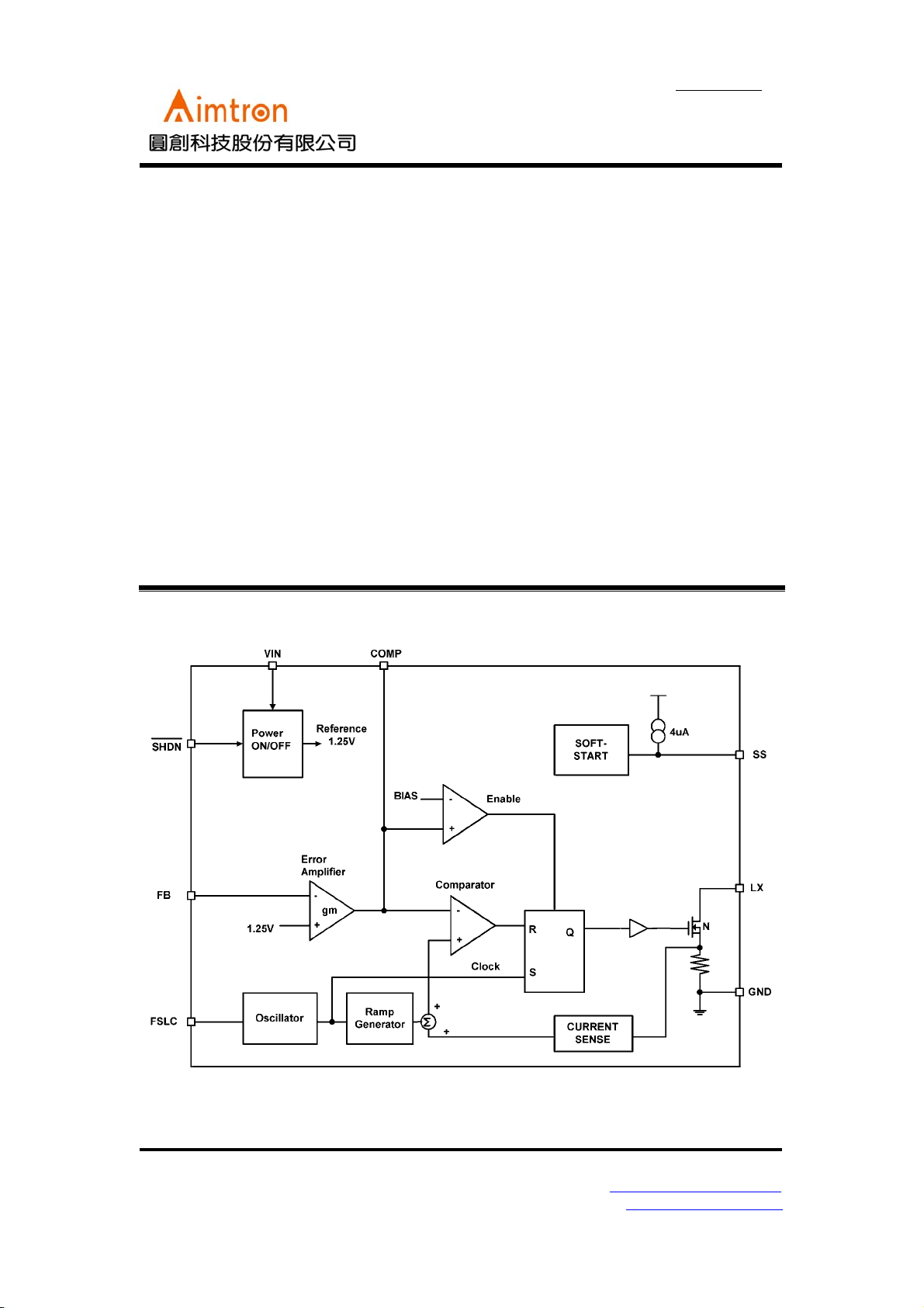
Block Diagram
General Description
The AT1780 is a current-mode step-up DC/DC
converter with a 1.8A, 0.21Ω power MOSFET.
The soft-start function is programmed with an
external capacitor, which sets the input current
ramp rate. It is ideal for generating bias voltages
for LCD panels. Pin selectable frequency 640KHz
or 1.2MHz operation results in a low noise output
that is easy to filter and faster loop performance.
An external compensation pin provides the user
flexibility in determining loop dynamics, allowing
the use of small, low equivalent series resistance
(ESR) ceramic output capacitors.
.
2F, No.10, Prosperity RD. II, Science-Based Industrial Park, Hsinchu 300,Taiwan, R.O.C.
Tel: 886-3-563-0878 WWW: http://www.aimtron.com.tw
Fax: 886-3-563-0879 Email: service@aimtron.com.tw
1
AT1780
640kHz/1.2MHz,Low-Noise Step-Up
Current-Mode PWM Controller
Pin Configuration
Preliminary
Ordering Information
Part number Package Marking
AT1780 8µMAX
Pin Description
Pin No. Symbol I/O Description
1 COMP - Compensation network connection.
2 FB I Output voltage feedback input
3 /SHDN I Shutdown control input, active low
4GND
5 LX O Switch Pin.
6VIN
7 FSLC I Frequency select input. Ground=640KHz, VIN=1.2MHz
8 SS — Soft-Start control pin.
Ground
-
Power supply pin.
-
2F, No.10, Prosperity RD. II, Science-Based Industrial Park, Hsinchu 300,Taiwan, R.O.C.
Tel: 886-3-563-0878 WWW: http://www.aimtron.com.tw
Fax: 886-3-563-0879 Email: service@aimtron.com.tw
2
AT1780
640kHz/1.2MHz,Low-Noise Step-Up
Current-Mode PWM Controller
Absolute Maximum Ratings
Preliminary
Rated ValueParameter Condition
Unit
Min. Max.
LX to GND — -0.3 +14 V
IN, /SHDN, FREG, FB to GND — -0.3 +8 V
SS, COMP to GND — -0.3 VIN+0.3 V
RMS LX pin current — — 1.2 A
Continuous power dissipation
8pin μMAX(TA=+70℃)
Operating temperature — -30 +85
Junction temperature — — +150
Storage temperature — -40 +150
Lead temperature — — +300
Stresses beyond those listed under “Absolute Maximum Ratings” may cause permanent damage to the device. These are
stress ratings only, and functional operation of the device at these or any other conditions beyond those indicated in the
operational sections of the specifications is not implied. Exposure to absolute maximum rating conditions for extended
periods may affect device reliability.
—330 mW
0
C
0
C
0
C
0
C
Recommended Operating Conditions
(Ta=+250C)
Power supply voltage V
SS pin capacitance C
Phase compensation capacitance C
Phase compensation capacitance C
Phase compensation resistance R
Oscillation frequency
f
f
Operating temperature T
CC
PE
COMP1
COMP2
COMP
OSC1
OSC2
OP
Va lu esParameter Symbol
Min. Typ. Max.
2.5 -- 7
-- 0.033 --
-- 680 --
-- 20 --
-- 180 -- KΩ
540 708 740 kHz
1000 1220 1500 kHz
-30 +25 +85 °C
Unit
V
μF
pF
pF
2F, No.10, Prosperity RD. II, Science-Based Industrial Park, Hsinchu 300,Taiwan, R.O.C.
Tel: 886-3-563-0878 WWW: http://www.aimtron.com.tw
Fax: 886-3-563-0879 Email: service@aimtron.com.tw
3
 Loading...