

Page 1

User and Service Guide
Publication number 01141-97002
July 2004
For Safety and Regulatory information, see the pages at the end
of this book.
© Copyright Agilent Technologies 2000-2004
All Rights Reserved
Agilent Technologies 1141A
Differential Probe and 1142A
Probe Control and Power
Module
Page 2

Agilent Technologies 1141A Differential Probe and
1142A Probe Control and Power Module
This manual contains information for use and service of the differential
probe system, the 1141A Differential Probe and 1142A Probe Control
and Power Module. In this document, the two models will be treated as
a system.
Each of the two instrument models that make up the differential probe
system has a serial number sticker. The sticker for the 1141A
Differential Probe is inside the probe, in the bottom cover. (See
chapter 3 for disassembly procedure.)
The 1141A/1142A probe system allows measurement of small
differential signals in the presence of much larger common-mode
signals. It has the following major features:
• 200 MHz bandwidth
• Variable offset
• dc reject
• ac coupling
• Remote operating capability
The variable offset capability can be used to measure small ac signals in
the presence of much larger dc levels. Remote operation of key
features allows the use of the probe system in automatic test situations.
The probe can be used with an oscilloscope, spectrum analyzer, or any
instrument where differential probing is required and a compatible
50 Ω input is available.
2
Page 3

Contents
1 Operating the Probe
Accessories Supplied 6
Accessories Available 8
To inspect the probe 9
Using the probe with other instruments 9
Recommended Test Equipment 9
2 Calibration Tests and Adjustment
Equipment Required 26
The Test Board 26
Calibration Tests 27
dc Gain Accuracy 28
Bandwidth 34
CMRR Test 36
Calibration Test Record 39
Adjustments 40
Probe Adjustment 40
Adjustment Procedure 42
Attenuator Adapter Adjustment 49
3Service
Introduction 54
Performance Specifications and Characteristics 55
General Characteristics 58
3
Page 4
Contents
Theory of Operation 59
Differential Probe 60
Control and Power Module 60
Attenuator Adapters 61
Test Board 62
Service Policy 63
Troubleshooting 64
Probe Troubleshooting 64
Probe Control and Power Module Troubleshooting 64
Removing and Replacing Assemblies 66
Differential Probe 66
Probe Adapters 68
Probe Control and Power Module 70
Replaceable Parts 71
Parts List 71
Ordering Information 71
Direct Mail Order System 71
Manufacturers’ Codes 72
Exploded View 73
4
Page 5

1
Operating the Probe
5
Page 6
Operating the Probe
Accessories Supplied
Introduction
This chapter shows you how to connect and operate the 1141A
Differential Probe and 1142A Probe Control and Power Module as a
differential probe system.
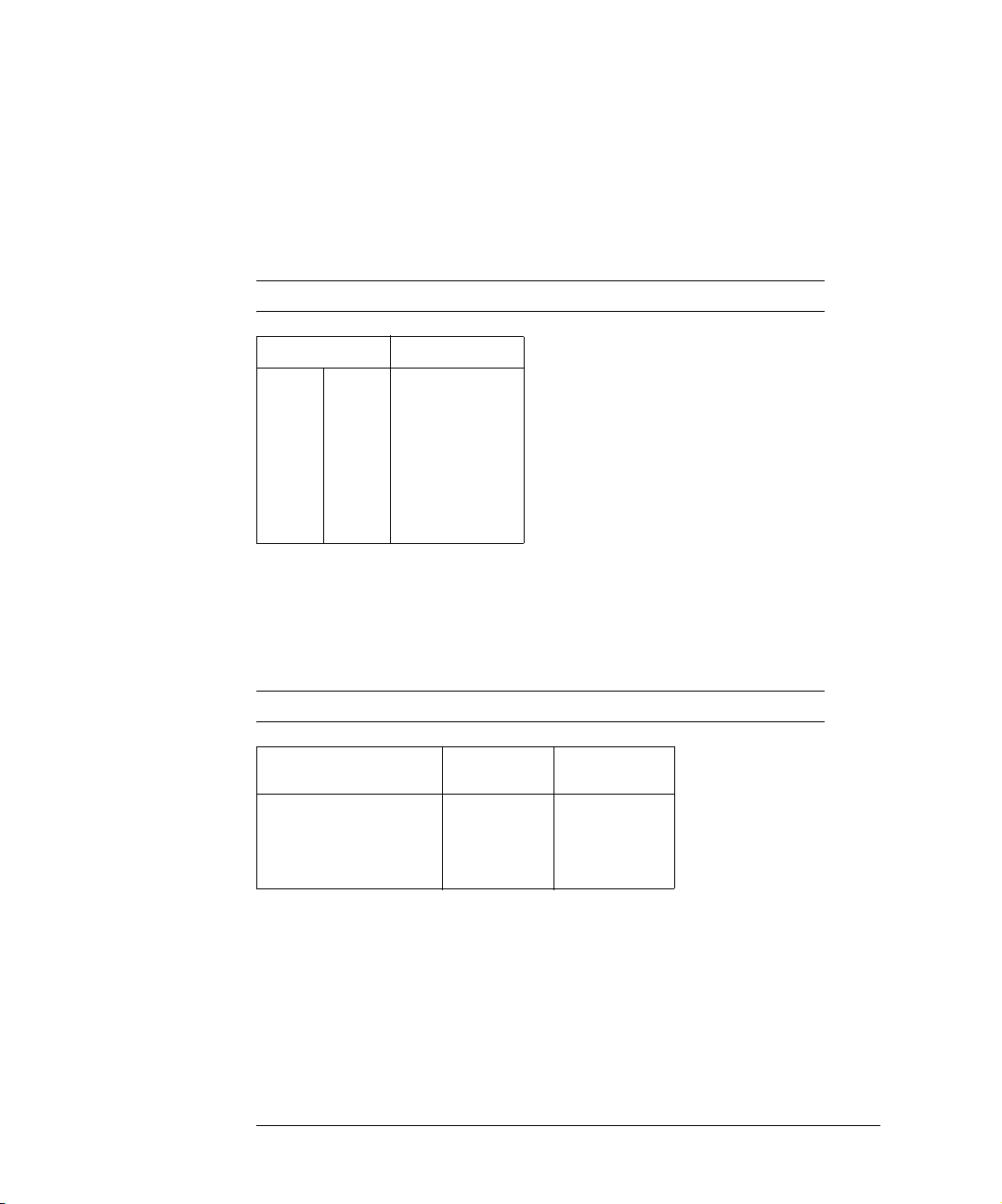
Accessories Supplied
The following items are supplied as part of the 1141A/1142A probe
system. Item numbers refer to the numbers in Figure 1-1 on page -7
and Figure 1-2 on page -8. Those without item numbers are supplied
but not shown in figures. See the Replaceable Parts List for parts not
listed below.
Item Description Qty Part Number
1 Differential Probe 1
2 10x Attenuator Adapter 1 5063-2144
3 100x Attenuator 1 5063-2145
4 ac Coupling Adapter 1 5063-2146
5 Two-inch Extension Leads (package 5) 1 5959-9334
6 Mini Grabbers 2 1400-1422
7 Five-inch Ground Lead 1 5061-6162
8 Shielded Signal Lead 1 01141-68702
9 Test Board 1 01141-66504
10 Flat-blade Alignment Tool 1 8710-1961
11 Circuit Connection Posts (strip of 20) 1 1251-5943
Probe Control and Power Module 1 1142A
Power Cord 1 see parts list
Carrying case
User and Service Manual 1
6
Page 7
Figure 1-1
Operating the Probe
Accessories Supplied
1141A Differential Probe and Accessories
7
Page 8
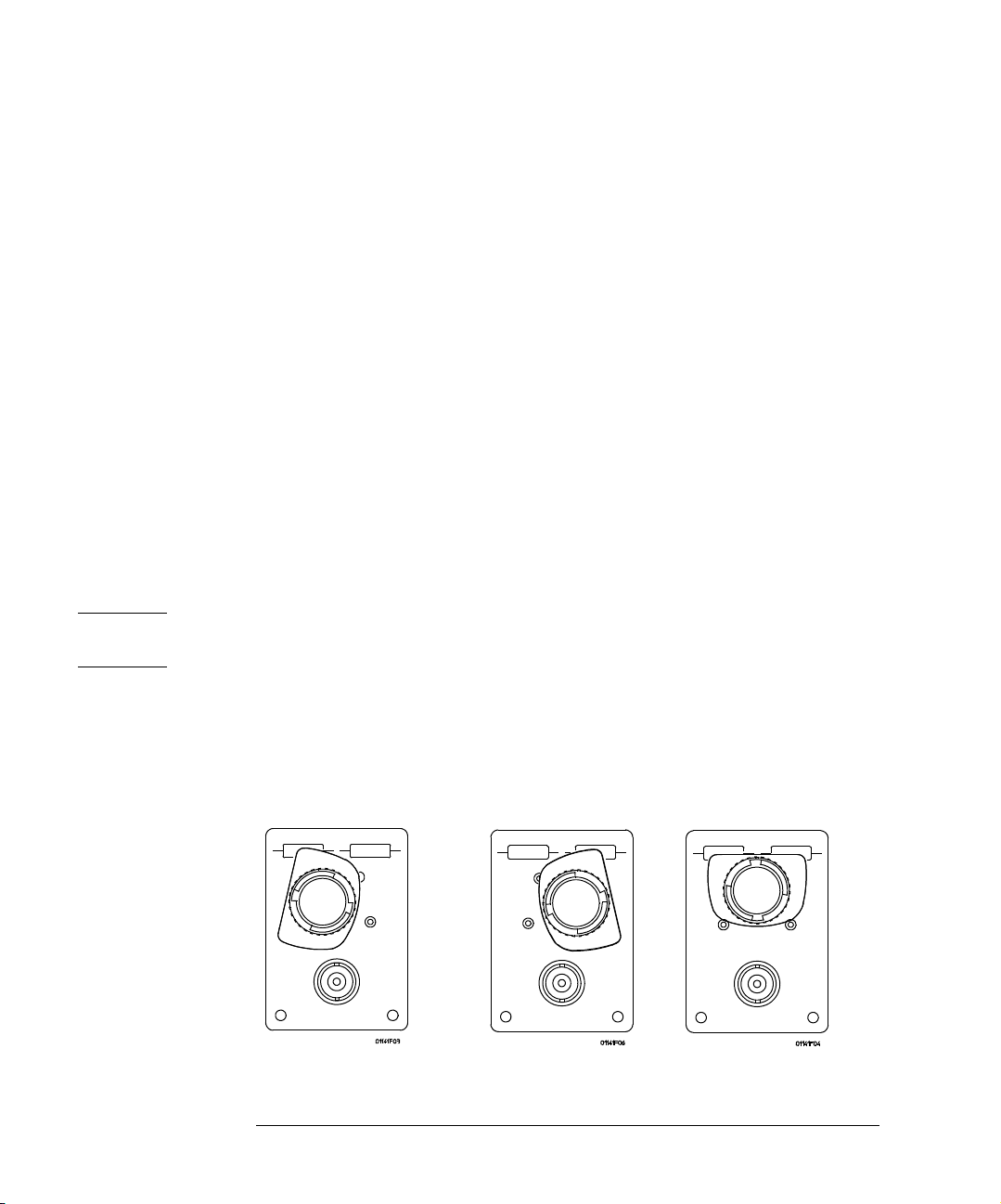
Figure 1-2
Figure 1-3
Operating the Probe
Accessories Available
1141A Miscellaneous Accessories
1142A Probe Control and Power Module
Accessories Available
The following accessories can be ordered.
• 5959-9335 Long Extension Lead (5.5 inch/14 cm), package of 5
• 5090-4833 Mini grabber for SMT, package of 20
8
Page 9

Operating the Probe
To inspect the probe
To inspect the probe
Inspect the shipping container for damage. If the shipping container or cushioning
material is damaged, it should be kept until the contents of the shipment have been
checked for completeness and the instrument had been checked mechanically and
electrically. Accessories supplied with the instrument are listed in see “Accessories
Supplied” on page 6 of this manual.
If the contents are incomplete, if there is mechanical damage or defect, or if the
instrument does not pass calibration tests, notify the nearest Agilent Technologies office.
If the shipping container is damaged, or the cushioning materials show sign of stress,
notify the carrier as well as the nearest Agilent Technologies office. Keep the shipping
materials for the carrier’s inspection. The office will arrange for repair or replacement
at Agilent Technologies’ option without waiting for a claim settlement.
Using the probe with other instruments
The 1141A/1142A probe system can be used with other instruments as well as
oscilloscopes. You can use it with a spectrum analyzer or frequency counter, or any
instrument with an input that can be terminated with 50 Ω.
If you are going to use the probe system with an instrument other than an oscilloscope,
you may need to set up the probe with an oscilloscope first. This will allow you to select
coupling and reject modes, and set offset, so the output of the probe is compatible with
signal requirements of the other instrument.
Recommended Test Equipment
The following table is a list of the test equipment required to test calibration, make
adjustments, and troubleshoot this instrument. The table indicates the critical
specifications of the test equipment and for which procedure the equipment is necessary.
Equipment other than the recommended model may be used if it satisfies the critical
specifications listed in the table.
Recommended Test Equipment
Recommended
Equipment Required Critical Specifications
Signal Generator 1 to 200 MHz, 400 m V
Function Generator 2.5 to 500 kHz, 600 m V
Oscilloscope >400 MHz bandwidth, 1 mV/div sensitivity 54830B P,A
dc source ± 100 mV to 7 Vdc E3632A P
rms
p-p
to 16 V
p-p
Agilent
Model/Part Use
8648A P
33120A A
9
Page 10

Operating the Probe
Recommended Test Equipment
Recommended
Equipment Required Critical Specifications
Test Board No substitute (supplied accessory) 01141-66504 A
Load BNC Feedthrough, 50 Ω Pasternack
Cables (2) BNC, 50 Ω 36-inch 10503A P,A
Cable BNC, 50 Ω 9-inch 10502A A
Cable Type N (m) 24-inch 11500B P
Adapter Type N (m) to BNC (f) 1250-0780 A
Adapter Type N (f) to BNC (m) 1250-0077 P
Adapters (2) BNC (f) to dual banana (m) 1251-2277 P
Agilent
Model/Part Use
P
Enterprises PE600850 or Huber+Suhner
22543742
Alignment tool Small flat blade (supplied accessory) 8710-1961/
Sprague-Goodman
part number GTT-5G
P=Calibration Tests, A=Adjustments
A
Setting up the probe
The following paragraphs cover system preparation and initial adjustments.
Power Requirements
The 1141A/1142A probe system (specifically the 1142A) requires a power source of
either 90 to 132/198 to 264 Vac, 47 to 440 Hz, 25 VA maximum.
CAUTION Before connecting power to this instrument, be sure the line voltage switch on the rear
panel of the instrument is set properly.
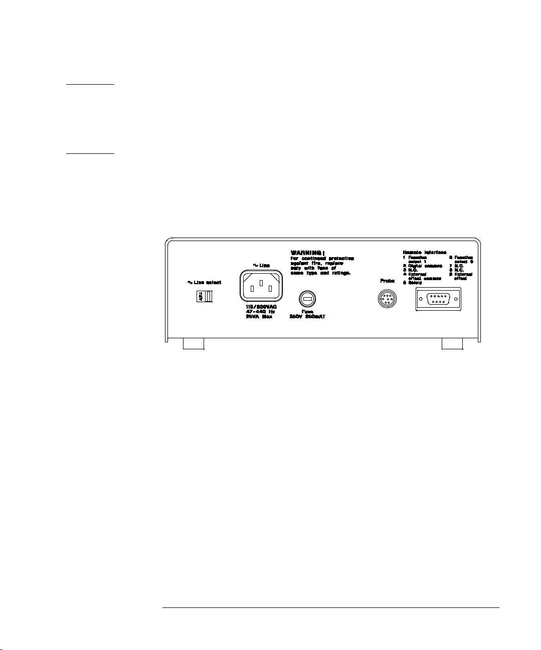
Line Voltage Selection
Before applying power, verify the setting of the LINE SELECT switch on the rear panel
of the 1142A. The slide switch can be set to either 115 or 230 V.
10
Page 11
Operating the Probe
Recommended Test Equipment
WARNING Before connecting this instrument, the protective earth terminal of the instrument must
be connected to the protective conductor of the (Mains) power cord. The Mains plug
must be inserted in a socket outlet provided with a protective each contact. The
protective action must be negated by the use on an extension cord (power cable)
without a protective conductor (grounding). Grounding one conductor of a twoconductor outlet does not provide an instrument ground.
This instrument is provided with a three-wire power cable. When connected to an
appropriate ac power outlet, this cable grounds the instrument cabinet. The type of
power cable plug shipped with the instrument depends on the country of destination.
The 1142A Power Control and Power Module does not have a power switch. A power
switch is not required because of the low mains power requirement.
Figure 1-4
1142A Rear Panel
Procedure
Use the power cord to connect the 1142A to the ac mains.
1
2 Connect the 1141A probe cable power connector to the PROBE connector on
the rear panel of the 1142A power module.
3 Connect the output of the probe to the input of the oscilloscope.
4 Set the input impedance of the oscilloscope to 50 Ω.
If the oscilloscope does not have a selectable 50 Ω input impedance, connect a 50 Ω BNC
feedthrough termination between the probe output and the input of the oscilloscope.
5 If making an initial equipment setup, continue with the initial adjustment in
the following section.
Initial Adjustment
For a given combination of 1141A Differential Probe and 1142A Probe Control and Power
Module, you may want to adjust the Offset Null and DC Reject Gain. Typically, you need
to make these adjustments only once, before the probe is first used. You can make them
any time to optimize the system. These adjustments do not affect the specifications of
the probe system.
11
Page 12
Figure 1-5
Operating the Probe
Recommended Test Equipment
• Offset null zeroes the dc level at the output of the probe. The range of adjustment is
about ±4 mV.
• DC Reject Gain adjusts the gain of the dc reject circuit to accurately null the dc
component of an input signal. The range of adjustment is about ±0.5%.
1142A Front Panel
Equipment Needed
The following equipment is necessary for initial adjustment.
• 5 V power supply
• DVM that can measure 25 µV
•50 Ω BNC feedthrough terminator
• 01141-66504 test board
Equipment Setup
Use the following procedure to setup the differential probe system for initial adjustment.
CAUTION Do not exceed ±7 V when using the test board for this procedure. If the voltage is too
high, it will cause excessive power dissipation in the 50 Ω termination on the test board.
1 Use the probe setup procedure to set up the probe system.
2 Connect a 50 Ω BNC feedthrough terminator to the output of the probe.
3 Disconnect all accessories from the input of the probe.
4 Connect the DVM to measure the dc output of the probe at the 50 Ω load.
12
Page 13
Figure 1-6
Operating the Probe
Recommended Test Equipment
5 Set up the 1142A:
a Set the Local/Remote push button to Local.
b Under DC Couple, press Zero offset.
6 Set the power supply output to 5 V.
7 Arrange a connection between the power supply and the test board. The
negative terminal of the supply should connect to the shield of the test board
BNC.
If your power supply has standard binding posts, you can connect a banana-to-BNC
adapter to the supply and connect a BNC cable between the supply and the test board.
Adjustment
Warm up the 1141A for 30 minutes before making adjustments.
1
With the 1141A probe inputs unconnected, adjust Offset Null on the 1142A for
a minimum reading on the DVM.
The voltage swing of the adjustment is approximately ±4 mV.
On the 1142A, under DC Reject, press 5.0 Hz.
2
3 Read and record the reading on the DVM, _________ mV.
4 Connect the probe to the test board in the position shown below
(signal to + input).
Signal to + input
5 After the DVM reading stabilizes, adjust DC Reject Gain to the reading recorded
in step 3.
With a 5 V supply, the voltage swing is approximately ±12.5 mV. With a lower supply, the
voltage swings proportionally less.
Using the Accessories
The 1141A Differential Probe and accessories are designed to provide a variety of ways
to connect to circuitry and make measurements. In the descriptions, any method used
to connect to the probe signal inputs also applied to the adapters. The figure below
shows, in a general way, the use of accessories.
13
Page 14
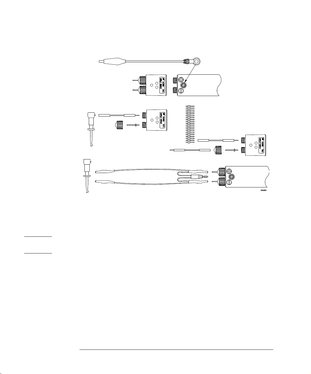
Figure 1-7
Operating the Probe
Recommended Test Equipment
Basic Accessory Connections
Probe Tips
Probe tips fit into the receptacles in the probe and are held in place with probe tip caps.
If necessary, you can solder the probe tips into a circuit or wires can be soldered to the
tips. If you solder to the probe tips, be careful not to melt the plastic probe tip caps.
Note Because of the close tolerances between the probe tip caps and probe tips, it will be
difficult to separate the probe tips and caps once the probe tips have been soldered.
Ground Leads
The circular end of the ground lead fits over the screw on the top side of the probe.
Extension Leads
The extension leads provide a flexible connection between circuitry and the probe.
• To provide a male connection to other circuitry, connect the extension lead over the
probe tips.
• To provide a female connection, remove the probe tip caps and probe tips and connect
the extension leads to the probe.
14
Page 15

Operating the Probe
Recommended Test Equipment
Note Use extension leads and similar connection accessories carefully. Extension leads
compromise the high-frequency specifications of the probe. CMRR is particularly
sensitive to unbalanced input parameters.
To prevent pickup of stray fields when you use extension lead, either the ones supplied
with the 1141A or others, dress them carefully as follows:
• Connect the leads at right angles to the circuitry under test.
• Keep the leads as parallel as possible before they connect to the probe.
Mini-Grabbers
Mini-grabbers can be attached to the probe or adapter through the extension leads.
1
Remove the probe tip caps and tips.
2 Attach the extension leads to the probe or adapter.
3 Attach the mini-grabbers to the extension leads.
Circuit Connector Posts
These 0.025-inch square posts can be used to connect either directly to the probe or to
the extension leads.
Solder the posts directly into your circuitry or use them to make extension leads that
plug into the inputs of the probe or adapters.
Shielded Signal Leads
The shielded signal leads allow connection to points in a circuit that are up to 10 inches
apart. The leads are shielded to within approximately 1/2 inch of the end of the lead so
they minimize pick-up due to stray fields from adjacent circuitry.
1
Connect the end with the ground connector to the probe pins and ground of
the differential probe or adapter.
2 Connect the free ends of the leads to 0.025-inch square or 0.030-inch round pins
in your circuitry or to the mini-grabbers.
Note Each lead has an input capacitance of approximately 15 pF. This capacitance may limit
the bandwidth of your measurement (depending on the impedance of the circuit). Also,
CMRR may be affected because of slight differences between the input capacitance of
the two leads. CMRR is also affected by differences in impedance between the two
measurements points.
15
Page 16
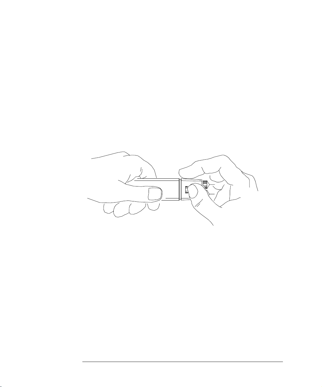
Figure 1-8
Operating the Probe
Recommended Test Equipment
Adapters
There are three adapters for use with the differential probe. Two adapters are
attenuators, a 10x and a100x. The other is an ac adapter for blocking dc from the probe
input.
The adapters are installed on the probe after the probe tip caps and probe tips have been
removed. The adapter fastens to the probe using a thumb wheel located on the underside
of the adapter. the figure below shows a good way to hold the probe while attaching the
adapter.
1
Remove the probe tip caps and probe tips, from the probe.
2 Fit the adapter over the end of the probe and rotate the thumb wheel with your
finger until the adapter fits snugly.
A snug fit is important because the ground is maintained through the thumb wheel screw.
A loosely attached adapter compromises the mechanical and electrical integrity of the
combination.
Attaching the Adapters
16
Page 17
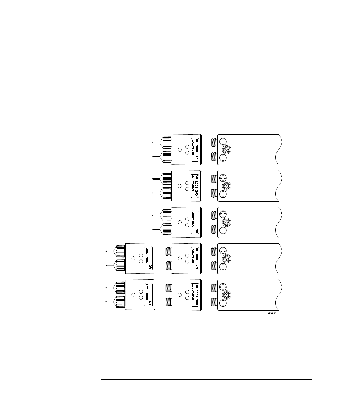
Figure 1-9
Operating the Probe
Recommended Test Equipment
Adapter Combinations
The figure below shows the allowed adapter and probe connections. There are two
specific combinations that should not be used.
• Do not attach the ac adapter between an attenuator adapter and the probe.
An attenuator adapter must be terminated by the input resistance of the probe. The
ac adapter isolates the probe input resistance.
• Do not cascade two attenuator adapters.
The attenuator adapters are designed to be terminated by the 1 MΩ resistance of the
probe. The input resistance of the attenuator adapter is 9 MΩ for the 10x adapter and
10 MΩ for the 100x adapter.
Allowed Adapter Connections
17
Page 18
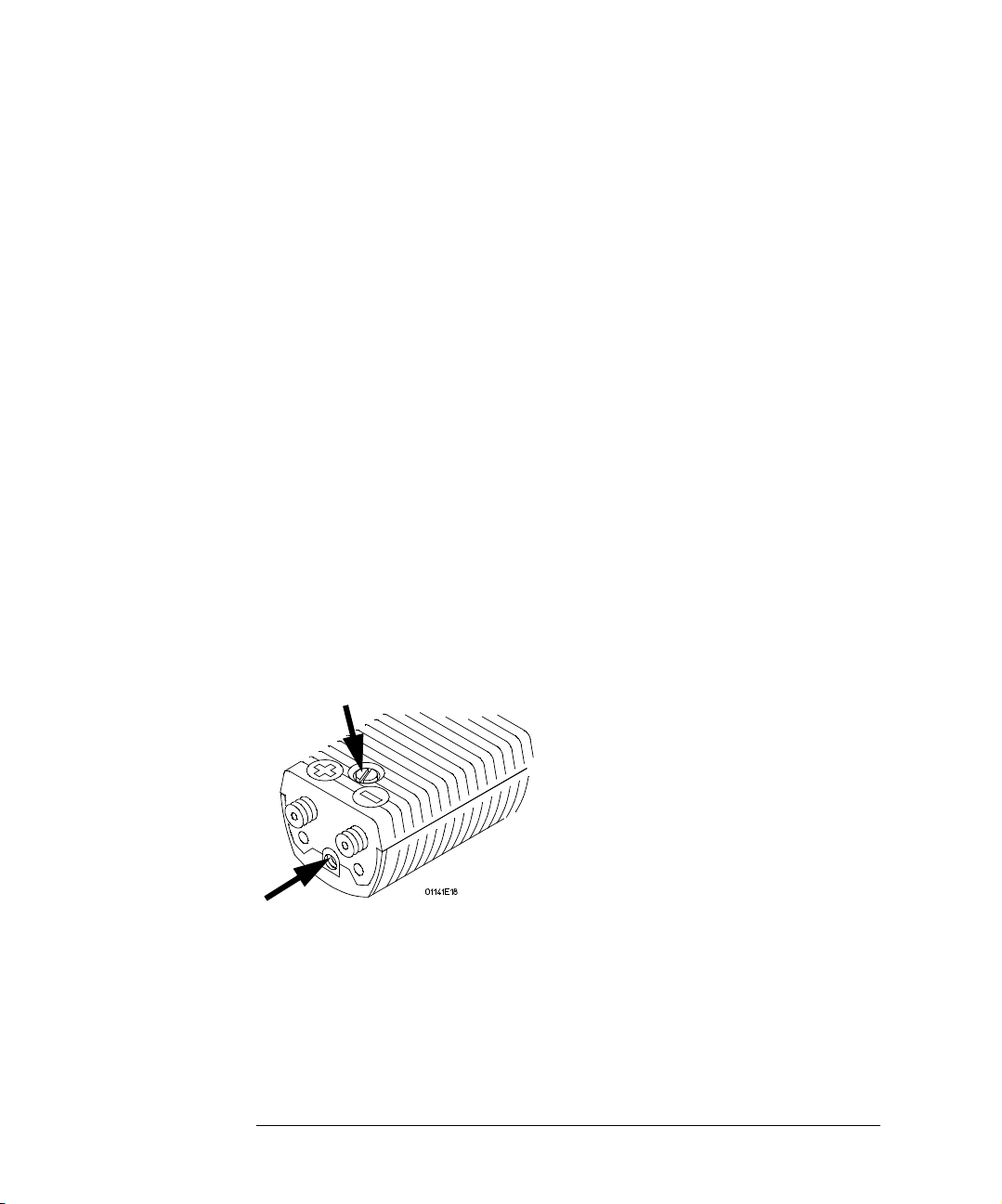
Figure 1-10
Operating the Probe
Recommended Test Equipment
Connector Compatibility
The following are general connector characteristics for the probe, adapters, and
accessories.
• The female connectors on the probe, adapters, and other accessories are designed to
mate with 0.030-inch round or 0.0250-inch square pins.
• The probe, adapter, and extension lead pins are 0.030-inch round.
• The strip of circuit connection posts provided as an accessory has 0.025-inch square
pins.
• The mini-grabber has a 0.25-inch square pin.
• The ground connection at the end of the probe and adapters (where the adapters
fasten) accepts an M3 metric screw.
Test Board
The primary use of the test board is to apply test and calibration signals to the input of
the probe or adapters. Specific use of the test board is covered wherever it applies.
Grounding
Grounding is very important when probing circuitry. Improper grounding can increase
the common mode signal level. This reduces the effectiveness of the differential probe.
The mechanical connections at the input of the probe are ground for probe signals. The
screw where the ground lead attaches (see figure 1-7) fastens to this ground. Also, the
attenuator and ac adapter fasten to this ground through the screw connection and the
ground is carried through each adapter to its front.
Probe Grounds
Coupling Functions
There are three methods for blocking or compensating for the dc component of a signal.
Each has specific advantages.
18
Page 19

Probe System Coupling Functions
Operating the Probe
Recommended Test Equipment
dc offset dc Reject ac Coupling
Adapter
dc Blocked
Probe alone
Probe with 10x
Probe with 100x
Set-up needed
± 20 V
± 200 V
± 500 V
Adjust offset to put
signal on screen
Remote Control? Yes
CMRR
No No Yes
1
± 20 V
± 200 V
± 500 V
Select DC Reject
low-frequency
corner
1
Yes
± 20 V
± 500 V
± 500 V
Attach ac Coupling
adapter to
differential probe
No
degradation?
Low-frequency
No Yes Yes
degradation?
1
Isolated external dc reference and control signals are needed
dc Reject
dc Reject is the best method of eliminating the dc component of a signal when dc is not
a factor in the measurement.
The key characteristics are:
• The low-frequency component (from dc to the selected corner frequency) is
automatically nulled by the dc reject circuitry.
• Probe CMRR specifications are not compromised as happens when the ac coupling
adapter is uses.
• There is a selectable low frequency corner with -3dB points at 0.05 Hz, 0.5 Hz,
or 5.0 Hz.
• The voltage reject range is ±20 V with the probe alone, ±200 V with the 10x attenuator,
and ±500 V with the 100x attenuator.
19
Page 20

Operating the Probe
Recommended Test Equipment
To use dc reject:
Remove the ac adapter if it is installed.
1
2 On the front panel of the 1142A, press Local.
3 Under DC Reject on the front panel, press 5.0 Hz or 0.5 Hz individually, or
5.0 Hz and 0.5 Hz simultaneously to get 0.05 Hz.
Within the frequency and voltage characteristics noted elsewhere in this manual, low
frequencies are nulled from the input signal.
Offset
Offset is the best method to use when the low-frequency corners associated with dc
reject and the ac adapter interfere with the measurement.
The key characteristics are:
• The user manually null the dc component with the offset adjustment.
• Offset is dc coupled so there is no low frequency roll-off.
• Probe CMRR specifications are not compromised as happens when the ac coupling
adapter is used.
• The voltage offset range is ±20 V with the probe alone, ±200 V with the 10x attenuator,
and ±500 V with the 100x attenuator. (With the 100x attenuator, the offset range is
restricted by the maximum input voltage rating rather than the operating range of
the offset).
To use offset:
1
Remove the ac adapter if it is installed.
2 On the front panel of the 1142A, press Local and Variable offset.
3 Adjust the Coarse and Fine Variable Offset until the signal is displayed on the
screen of the oscilloscope.
ac Adapter
The ac adapter must be used when the dc component of the signal exceeds the operating
range of the dc reject or offset methods. The ac adapter block the dc and low frequency
component of the input by forming a high pass filter with the input impedance of the
probe or adapter.
The key characteristics are:
• The ac adapter safely blocks ±200 Vdc when attached directly to the probe or
±500 Vdc when attached to a 10x or 100x adapter.
• The probe and adapters have different input impedances, so they have different low
frequency corners with the ac adapter. When the ac adapter is directly on the probe
the -3dB corner is 15 Hz. When the ac adapter is on an attenuator the corner is 1.5 Hz.
• The low-frequency CMRR when using the ac adapter is not as good as when using the
probe alone or the probe with a 10x or 100x adapter.
CAUTION If you measure a node having a high dc potential, the blocking capacitors in the ac
adapter will charge to that potential. After making such measurements, discharge the
capacitors by grounding both inputs of the ac adapter. This will prevent damage by a
high voltage discharge into sensitive circuitry when the next measurement is made.
20
Page 21
Operating the Probe
Recommended Test Equipment
To use ac coupling:
Attach the ac coupling adapter to the input of the probe or the input of the
1
attenuator adapter.
2 On the 1142A, press Local and Zero offset.
Remote operation
For automatic test applications, the coupling and offset functions provided by the 1142A
Probe Control and Power Module can be remotely controlled through a connector on the
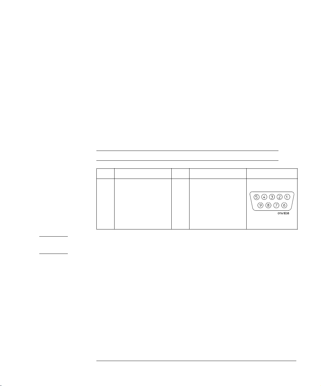
rear panel of the module. The connection is through a standard 9-pin female
D-subminiature connector. This style is the same as that used on some personal
computer monitor cables, which provides an economical way to connect the 1142A to
the controller interface on an automatic test system.
The following table gives the connections.
Remote Input Connections
Pin Function Pin Function Connector
1 Function Select 1 (A1R) 6 Function Select 0 (A0R)
2 Digital common 7 N.C.
3N.C. 8N.C.
4 External offset common 9 External offset
5 Shield
NOTE To minimize dc offset errors and potential noise coupling, electrically isolate all
connections between the Remote Input connector and the controlling system.
21
Page 22
Operating the Probe
Recommended Test Equipment
Function Select
The easiest way to control the function select lines is contact closures between the lines
and Digital common (pin 2) of the remote input connector. (TTL compatible control
signals can be used; but to avoid problems with ground loops, they must be electrically
isolated.) The following truth table shows the functions provided by the function select
lines. For the Remote Inputs, “0” represents a closure and “1” represents an open circuit.
Remote Functions Select Truth Table
Remote Input Function
A1R
(Pin 1)
0 0 0.05 Hz Reject
0 1 0.5 Hz Reject
105 Hz Reject
1 1 DC Couple
Variable Offset
The remote variable offset can be used when the dc couple function is remotely selected.
The offset voltage must be referenced to the External offset common (pin 4) of the
remote input connector. It must be electrically isolated from the controlling system. The
following table shows the offset range and remote offset requirements for probe and
adapter combinations.
Remote Offset Input Requirements
Probe alone ± 20 V ± 10 V
Probe with 10x adapter ± 200 V ± 10 V
Probe with 100x adapter ± 500 V ± 2.5 V
A0R
(Pin 6)
Offset Range Remote
Requirements
Cleaning Requirements
If the instrument requires cleaning: (1) Remove power from the instrument. (2) Clean
the external surfaces of the instrument with a soft cloth dampened with a mixture of
mild detergent and water. (3) Make sure that the instrument is completely dry before
reconnecting it to a power source.
22
Page 23

Operating the Probe
Recommended Test Equipment
Differential Amplifiers and CMRR
The 1141A Differential Probe is a high-impedance differential amplifier. A characteristic
of differential amplifiers is the ability to reject signals that are common to the two inputs.
The common mode rejection ratio (CMRR) is the measurement of this ability. It is
expressed as the ratio between the amplitudes of the common mode and differential
signals which product equal outputs. For example, if a common mode signal of 1 V and
differential signal of 1 mV both produce outputs of 1 mV, the CMRR is 1000:1.
The ability to reject common mode signals is dependent on the balance designed into
the differential amplifier. At higher frequencies it becomes harder to balance circuit
parasitics and parameters of devices so CMRR degrades as frequency increases. Also,
stray coupling increases with frequency and coupling may vary between the two
differential paths.
The CMRR of the 1141A Differential Probe is specified at the input of the probe and
cannot be affected expect by adjustments in the probe. However, the way the probe is
connected into the circuitry being tested can have a big influence in the overall result of
the measurement, especially at high frequencies.
The following things can affect the effective CMRR of a test setup:
• The connection to the circuit under test.
The method used to connect the probe is important because it involves the symmetry
of the differential input circuitry. For example, using different lengths of wire to
connect the circuit to the two probe inputs unbalances the inductance and
capacitance at the inputs. The effective CMRR will be reduced, especially at high
frequencies. Additionally, coupling from adjacent circuitry will be less balanced.
• The impedance of the source.
This is another instance where the symmetry of the differential circuit is important.
The impedance of the source forms a network with the input impedance of the source
forms a network with the input impedance of the connections and the probe. This
network determines the frequency response for the measurement. If each side of the
differential source has a different impedance, the frequency response of each side
will be different and the unbalance is reflected in a reduced CMRR. Of course, lower
source impedances have less effect on the frequency response of the measurement.
• The ground connection.
A poorly located ground connection allows ground loops to add to the common mode
signal.
• Frequency.
Frequency is the most important factor in CMRR only because all of the factors
mentioned above are frequency dependent. The unbalances of capacitance and
inductance are more important as frequency increases. Therefore, good highfrequency practice is important when using a high impedance differential probe.
On the other hand, if the differential probe is ac coupled to the circuit under test (the
ac adapter is being used) the CMRR will be degraded below a certain frequency; the
lower the frequency the worse the CMRR. This is because unbalance in the series
capacitances of the ac coupler becomes more significant the lower the frequency.
23
Page 24

Operating the Probe
Recommended Test Equipment
24
Page 25

2
Calibration Tests and Adjustment
25
Page 26
Calibration Tests and Adjustment
Equipment Required
Introduction
This chapter is divided into two sections. The first section gives
calibration tests and the second adjustment procedures for the 1141A
Differential Probe and 1142A Probe Control and Power Module.
Equipment Required
A complete list of equipment required for the calibration tests and adjustments is listed
in “Recommended Test Equipment” on page 9. Equipment required for individual
procedures is listed at the procedure. Any equipment satisfying the critical specifications
listed may be substituted for the recommended model.
The Test Board
The test board is a supplied accessory for use during calibration tests and adjustments
to connect signals to the differential probe (with or without adapters). A BNC connector
connects the test board to a cable from the signal generator. The board includes a 50 Ω
termination (two 100 Ω resistors).
CAUTION The power rating of the 50 Ω termination is 1.0 W. Keep the signal input below 7 Vdc
or rms to avoid degrading the termination.
Once the probe tip caps and probe tips have been removed, the probe can be connected
to the test board in one of three ways, as shown in the figure below. At each position of
the probe, probe inputs are connected to a different combination of signal and ground.
A separate terminal on the test board connects the ground of the probe to the signal
ground.
Figure 2-1
Test Board Showing Probe Positions
26
Page 27

Calibration Tests and Adjustment
The Test Board
Calibration Tests
These procedures test the probe’s electrical performance using applicable specifications
given in “Performance Specifications and Characteristics” on page 55 as performance
standards. Specifications applicable to individual tests are noted at the test for reference.
Testing Interval
The calibration testing procedures may be performed for incoming inspection of the
instrument and should be performed periodically thereafter to ensure and maintain peak
performance. The recommended test interval is yearly or every 2,000 hours of operation.
Amount of use, environmental conditions, and the user’s experience concerning need
for testing will contribute to verification requirements.
Calibration Test Record
The results of the calibration tests may be tabulated in the Calibration Test Record
provided at the end of the calibration tests. The Calibration Test Record listed the
calibration tests and provides an area to mark test results. The results recorded in the
Calibration Test Record during initial inspection may be used for later comparisons of
the tests during periodic maintenance, troubleshooting, and after repairs or adjustments.
Calibration Test Procedures
Procedures may be done individually or in any order.
NOTE Allow the instrument to warm up for at least 30 minutes prior to beginning calibration
tests.
27
Page 28

Calibration Tests and Adjustment
dc Gain Accuracy
dc Gain Accuracy
This test checks the dc gain accuracy of the differential probe and the dc accuracy of
the differential probe with attenuator and adapters.
Specification: Probe alone, ±2%; with attenuator adapter, ±4%
Equipment Required
Equipment
Required Critical Specifications
ac/dc Calibrator
or
dc Power Supply
DVM 0.5% accuracy, 10 µV resolution 3458A or
Load BNC Feedthrough, 50 Ω Pasternack
Cables (2) BNC 50 Ω 10503A
Adapters (2) BNC (f) to dual banana (m) 1251-2277
Test Board No substitute 01141-66514
Probe Gain Test Procedure
Connect the probe and test equipment as shown in figure 2-2.
1
100 mV to 7 V
100 mV to 7 V
Recommended
Agilent
Model/Part
E3632A
E34401A
Enterprises
PE6008-50 or
Huber+Suhner
22543742
28
Page 29

Figure 2-2
Calibration Tests and Adjustment
dc Gain Accuracy
2
Set up the 1142A probe control and power module as follows:
a Set the Local/Remote push button to Local.
b Under DC Couple, press the Zero offset button.
With the 1141A Probe Amp disconnected from the test PCA, adjust the Offset
3
Null control on the 1142A until the DVM reads 0Vdc.
If the probe output voltage cannot be set to 0V, subtract this voltage from the subsequent
measurements in this test.
4 Connect the input of the Probe Amp to the test board in the position shown in
Figure 2-4 on page -31.
5 Adjust the DC Source to output 100 mV (nom.)
6 Record the V
7 Record the V
8 Connect the Probe Amp to measure a negative voltage as shown in figure 2-3.
9 Record the V
measurement from the top DVM in figure 2-2.
in1
measurement from the bottom DVM in figure 2-2.
out1
measurement from the bottom DVM in figure 2-2
out2
29
Page 30

Figure 2-3
Calibration Tests and Adjustment
dc Gain Accuracy
Signal to - input
10 Calculate probe gain as
∆V
out
--------------
∆V
Record the result of this calculation in the “Calibration Test Record” on page 39.
To pass this test, the probe gain = 0.98 to 1.02
NOTE Failure of the gain accuracy test can be caused by mis-adjustment of the probe. Perform
the Probe Adjustment procedure in the Adjustments section later in this chapter and
retest.
10x Attenuator Accuracy Test
NOTE If the gain test for the probe fails, the 10x Attenuator Accuracy Test will fail or the
results will be poor. Do not continue until the probe passes the dc gain test.
1 Disconnect the probe from the test board and connect the 10x attenuator
V
----------------------------------=
in
V
–()
out
2 V
out
1
×
in
2
1
adapter to the probe.
2 Carefully connect the input of the probe/attenuator to the test board in the
position shown in the figure below (signal to + input).
30
Page 31

Figure 2-4
Figure 2-5
Calibration Tests and Adjustment
dc Gain Accuracy
Signal to + input
3 Set the dc calibrator output 3 V dc.
4 Record the V
5 Record the V
6 Carefully connect the input of the probe/attenuator to the test board in the
measurement from the top DVM in figure 2-2.
in1
measurement from the bottom DVM in figure 2-2
out1
position shown in the figure below (signal to - input).
Signal to - input
7 Record the V
8 Calculate the 10x attenuator gain as
Record the result of this calculation in the “Calibration Test Record” on page 39.
NOTE Failure of the accuracy test for the 10x attenuator can be caused by mis-adjustment of
the low-frequency CMRR (LF CMRR) adjustment. Perform the Attenuator Adapter
Adjustment procedure in the Adjustments section later in this chapter then retest the
attenuator adapter. If if continues to fail, repair is necessary.
measurement from the bottom DVM in figure 2-2.
out2
∆V
out
--------------
∆V
in
V
----------------------------------=
V
–()
out
2 V
out
1
×
in
2
1
31
Page 32

Calibration Tests and Adjustment
dc Gain Accuracy
100x Attenuator Accuracy Test
NOTE If the gain test for the probe fails, it will be reflected in the test for the 100x attenuator
adapter. Do not continue until the probe passes the gain test.
1 Disconnect the probe/attenuator from the test board. Remove the 10x
attenuator adapter from the probe and connect the 100x attenuator adapter.
2 Carefully connect the input of the probe/attenuator to the test board in the
position shown in the figure below (signal to + input).
Figure 2-6
Signal to + input
CAUTION Avoid excessive power dissipation in the termination on the test board. Keep the voltage
input at or below ±7 Vdc.
3 Set the dc source output to 7 Vdc.
4 Record the V
5 Record the V
measurement from the top DVM in figure 2-2.
in1
measurement from the bottom DVM in figure 2-2
out1
32
Page 33

Figure 2-7
Calibration Tests and Adjustment
dc Gain Accuracy
6 Carefully connect the input of the probe/attenuator to the test board in the
position shown in the figure below (signal to - input).
Signal to - input
7 Record the V
8 Calculate the 100x attenuator gain as
Record the result of this calculation in the “Calibration Test Record” on page 39
NOTE Failure of the accuracy test for the 100x attenuator can be caused by mis-adjustment
of the low-frequency CMRR (LF CMRR) adjustment. Perform the Attenuator Adapter
Adjustment procedure in the Adjustments section later in this chapter then retest the
attenuator adapter. If if continues to fail, repair is necessary.
measurement from the bottom DVM in figure 2-2.
out2
∆V
out
--------------
∆V
in
V
----------------------------------=
V
–()
out
2 V
out
1
×
in
2
1
33
Page 34

Calibration Tests and Adjustment
Bandwidth
Bandwidth
This test checks the high-frequency response of the 1141A Differential Probe. The
bandwidth of the oscilloscope is characterized first so it is not a factor in the
measurement.
Specification (-3dB, dc coupled): dc to 200 MHz
Equipment Required
Equipment
Required
Oscilloscope 400 MHz bandwidth 54830A
Signal Generator 200 MHz at ≈ 230 mVrms 8648A
Test Board No substitute 01141-66504
Cable Type N (m) 24-inch 11500B
Adapter Type N (f) to BNC (m) 1250-0077
Procedure
This test depends on the accuracy of the termination on the test board and the
termination in the oscilloscope. Both should be with 1%.
With the N cable and N-to-BNC adapter, connect the signal generator to the
1
Critical Specifications Recommended
Model/Part
oscilloscope channel 1 input.
2 Set the signal generator for 200 MHz at 0 dBm (about 224 mVrms).
3 Set the 1142A front panel switches to Local and Zero offset.
4 On the oscilloscope press AUTOSCALE, then set the following parameters.
Menu Selection Setting
TIMEBASE (time/div) 2 ns/div
CHAN 1 (sensitivity)
(input R)
ACQUISITION Sampling Mode
Memory Depth
Sample Rate
Averaging
# of avg
100 mV/div
50 Ω DC
Real Time
Automatic
Automatic
Enabled
32
5 The signal on screen should be about six divisions amplitude.
Measure the peak-to-peak voltage of the channel 1 signal and record the
reading.
V
(1) = _____________ mV
p-p
34
Page 35

Figure 2-8
Calibration Tests and Adjustment
Bandwidth
6 Reconfigure the equipment.
a Disconnect the signal generator cable from the oscilloscope input and connect it to
the test board.
b Connect the output of the differential probe to the channel 1 input of the
oscilloscope.
c Carefully connect the input of the probe to the test board in the position shown in
the figure below (signal to + input).
Signal to + input
7 Record the V
V
(1) = _____________ mV
p-p
8 Divide the reading from step 6 by the reading from step 4.
Answer from step 6
----------------------------------------------Answer from step 4
reading on the oscilloscope.
p-p
____________ =
Record the result in the Calibration Test Record.
The result should be 0.707 or greater, indicating a probe bandwidth of 200 MHz or more.
The bandwidth can be checked at other signal levels. Change the signal generator output
level and oscilloscope V/div range proportionally.
NOTE Failure of the bandwidth test can be caused by mis-adjustment of the probe. Perform
the Probe Adjustment procedure in the Adjustments section later in this chapter.
35
Page 36

Calibration Tests and Adjustment
CMRR Test
CMRR Test
This test checks the CMRR at 1 MHz and 100 MHz.
Specification 3000:1 at 1 MHz, 10:1 at 100 MHz
Equipment Required
Figure 2-9
Equipment
Required Critical Specifications
Oscilloscope 400 MHz bandwidth at 1 mV/div 54830B
Signal Generator 1-100 MHz at = 400 mVrms 8648A
Test Board No substitute 01141-66504
Cable Type N (m) 24-inch 11500B
Adapter Type N (f) to BNC (m) 1250-0077
Procedure
Connect the probe power connector to the PROBE connection on the rear of
1
Recommended
Agilent
Model/Part
the 1142A Probe Control and Power Module.
2 Set the 1142A front panel switches to Local and Zero offset.
3 Connect the probe output to the oscilloscope channel 1 input.
4 Connect the input of the probe to the test board in the position shown in the
figure below (signal to + input).
Signal to + input
5 Connect the signal generator to the test board.
6 Set the signal generator for 1 MHz at 385 mV
rms
36
(1 V
p-p
).
Page 37

Figure 2-10
Calibration Tests and Adjustment
CMRR Test
7 On the oscilloscope, press AUTOSCALE and set the following parameters.
Menu Selection Setting
TIMEBASE (time/div) 500 ns/div
CHAN 1 (sensitivity)
(input R)
ACQUISITION Sampling Mode
Memory Depth
Sample Rate
Averaging
# of avg
200 mV/div
50 Ω DC
Real Time
Automatic
Automatic
Enabled
32
8 On the oscilloscope, measure the peak-to-peak voltage of the channel 1 signal,
then V P-P, then press 1) and record the reading.
V
(1) = _____________ mV
p-p
9 Connect the input of the probe to the test board in the position shown in the
figure below (signal to both inputs).
Signal to both input
10 Set the sensitivity to 1 mV/div.
11 After the measurement settles (averaging is complete), record the V P-P
reading.
V
(2) = _____________ mV
p-p
12 Disconnect the probe amp from the test board and measure V
channel 1.
noise pp
on
13 Calculate the CMRR result as follows
V
pp
CMRR
-------------------------------------=
V
pp
1
V
–
noisepp
2
14 The result in step 12 should be ≥ 3000, representing a CMRR of 3000:1 or more.
Record the CMRR in the Calibration Test Record.
37
Page 38
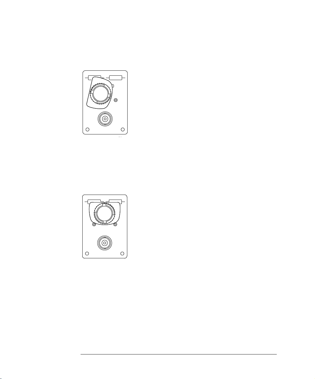
Figure 2-11
Calibration Tests and Adjustment
CMRR Test
15 Connect the input of the probe to the test board in the position shown in the
figure below (signal to + input).
Signal to + input
Figure 2-12
16 Set the signal generator for 100 MHz at 0.0 dBm (about 224 mV
, 632 mV
rms
p-p
17 Set the oscilloscope to channel 1 and change the horizontal scale to 5 ns/div.
18 After the measurement settles (averaging is complete), note the V P-P reading.
V
(1) = _____________ mV
p-p
19 Connect the input of the probe to the test board in the position shown in the
figure below (signal to both inputs).
Signal to both input
20 Set the channel 1 sensitivity to 10 mV/div.
21 After the measurement settles (averaging is complete), not the V P-P reading.
V
(2) = _____________ mV
p-p
22 Disconnect the probe amp from the test board and measure V
channel 1.
noise pp
on
23 Calculate the CMRR result as follows
V
pp
CMRR
-------------------------------------=
V
pp
1
V
–
noisepp
2
24 The result in step 21 should be ≥ 10, representing a CMRR of 10:1 or more.
Record the CMRR in the Calibration Test Record.
).
38
Page 39

Calibration Tests and Adjustment
Calibration Test Record
Calibration Test Record
1141A/1142A Differential Probe Tested by_________________________
Serial No. ______________________________ Work Order No.____________________
Recommended Test Interval - 1 Year/2000 hours Date____________________
Recommended next testing_________________ Temperature_____________
Test Limits Results
dc Gain Accuracy Probe
Only
+0.98 mV to +1.02 mV _____________
10x +0.096 mV to +0.104 mV _____________
100x +0.0096 mV to 0.0104 mV _____________
Bandwidth >0.707 at 200 MHz _____________
CMRR 1 MHz ≥3000:1 _____________
100 MHz ≥10:1
39
Page 40

Calibration Tests and Adjustment
Probe Adjustment
Adjustments
This section provides adjustment procedures for the 1141A Differential Probe and
attenuator adapters. There are no service adjustments for the 1142A Probe Control
Module.
Adjustment Interval
None of the adjustment procedures that follow should be considered for a routine
maintenance plan. The differential probe and attenuator adapters should be adjusted
under conditions specified at the beginning of the respective procedures.
NOTE Warm up the instrument for 30 minutes before starting adjustment procedures.
Probe Adjustment
This procedure adjust the high-frequency and low-frequency paths on the 1141A
Differential Probe.
NOTE Do not perform this procedure as a part of routine maintenance. Perform the procedure
only if the probe does not meet specifications or has been repaired.
CAUTION You are going to remove the covers of the probe, so the assembly inside will be exposed
while under power. The PC assembly will be electrically and mechanically vulnerable.
Do these adjustment procedures in an ESD-safe area.
Avoid inadvertent contact between the powered assembly and nearby tools and
equipment.
Avoid mechanical damage by carefully handling the exposed assembly and cables.
40
Page 41

Calibration Tests and Adjustment
Probe Adjustment
The following equipment is required for this procedure. Procedures are based on the
model or part number recommended.
Equipment Required
Equipment Required Critical Specifications Recommended
Function Generator 2.5 kHz, 1 V
Oscilloscope 300 MHz at 1 mV/div 54830B
Signal Generator 200 MHz at ≈ 300 mVrms 8648A
Test Board No substitute 01141-66504
Cables (2) BNC, 50 Ω 10503A
Adapter Type N (m) to BNC (f) 1250-0780
Probe Preparation
The probe cover must be removed before adjustment. Drift due to temperature
differences with and without covers is negligible.
1
Remove the probe tip caps and probe tips.
2 Loosen the probe clamp ring at the cable end of the probe (1/4 turn counter-
p-p
Agilent
Model/Part
33120A
clockwise) and slide it down the cable.
3 Remove the bottom cover.
a At the cable end of the probe, separate the covers about centimeter (1/2 inch).
b Slide the bottom cover toward the cable end of the probe until the locator pins at
the probe input clear the holes. Then, remove the cover.
NOTE Note the position of the ground block at the input end of the probe. The ground block
is held, through the PC assembly, by the grounding screw on the top of the probe. The
ground block must be reinstalled on the PC assembly after the top cover is removed.
Handle the PC assembly by the edges of the PC board.
4 Remove the ground connection screw on the top of the probe.
The ground block will become free.
At the cable end, the PC board fits over pins inside the top cover.
Lift the board off of the pins in the cover and slide it in the direction of the
5
cable until the input connectors clear the front of the probe.
41
Page 42

Figure 2-13
Calibration Tests and Adjustment
Adjustment Procedure
6 As shown in the figure below, use the grounding screw to reinstall the ground
block on the PC assembly.
Attaching Ground Block to Probe PC Assembly
The ground block provides a mechanical and electrical connection when the probe PC
assembly is connected to the test board.
7 Connect the probe power connector to the PROBE connection on the rear of
the 1142A Probe Control and Power Module.
8 Connect the mains power to the 1142A.
9 Set the 1142A front panel switches to Local and Zero offset.
Adjustment Procedure
Unless specified elsewhere, the procedures must be followed in the order given.
The only adjustment which may be done separately is HF COMP, the high-frequency
compensation.
HF Gain and HF CMRR
This adjustment sequence adjusts the HF Gain for unity gain at 500 kHz and the HF
CMRR for minimum with a 500 kHz common mode signal.
1
Set up the function generator.
• Sine wave
• 500 kHz
•600 mV
2 Use BNC cables to connect the function generator to the oscilloscope.
• Generator OUTPUT to oscilloscope channel 1 input
• Generator TRIG OUTPUT to oscilloscope EXT TRIG
42
p-p
Page 43

Calibration Tests and Adjustment
Adjustment Procedure
3 On the oscilloscope, then press CLEAR DISPLAY. Press AUTOSCALE, then set
up the following parameters.
Menu Selection Setting
TIMEBASE (time/div) 500 ns/div
CHAN 1 (sensitivity)
(input R)
TRIG (mode)
source
level
100 mV/div
50 Ω DC
trg’d
EXT
1.00000 V
Figure 2-14
ACQUISITION Sampling Mode
Memory Depth
Sample Rate
Averaging
# of avg
4 On the oscilloscope, measure the peak-to-peak voltage of the channel 1 signal
Real Time
Automatic
Automatic
Enabled
32
and record the reading.
V
(1) = _____________ mV
p-p
5 Disconnect the BNC cable from the channel 1 input and connect it to the BNC
connector on the test board.
6 Connect the output of the probe to the channel 1 input.
7 Carefully connect the input of the probe to the test board in the position shown
in the figure below (signal to + input).
Signal to + input
43
Page 44

Figure 2-15
Calibration Tests and Adjustment
Adjustment Procedure
8 Center adjustment R11, HF CMRR (see following figure).
R11, HF CMRR Adjustment
Figure 2-16
9 Adjust R9, HF GAIN so the V
±0.5%.
Make the adjustment slowly so the oscilloscope display has time to react to signal
averaging. Press CLEAR DISPLAY occasionally to restart averaging, which gives a
quicker indication of changes.
10
Carefully connect the probe to the test board in the position shown in the figure
(1) measurement is the same as in step 4, within
p-p
below (signal to both inputs).
Signal to both inputs
11 Set the function generator output to 1.0 V
12 On the oscilloscope, set the channel 1 sensitivity to 1.00 mV/div.
13 Adjust R11 for minimum signal amplitude as shown in V
channel 1. Adjust R11 slowly and use CLEAR DISPLAY frequently to restart
p-p
.
reading for
p-p
averaging.
Low Frequency Response and CMRR
This adjustment sequence continues from the HF Gain and HF CMRR adjustments.
Adjust R14 and C4 for pulse response, and adjust C6 for low-frequency CMRR.
1
Change the function generator settings to:
• Square wave
• 2.5 kHz
•600 mV
p-p
44
Page 45

Figure 2-17
Calibration Tests and Adjustment
Adjustment Procedure
2 Change the oscilloscope settings to:
Menu Selection Setting
TIMEBASE (time/div) 50 µs/div
CHAN 1 (sensitivity) 100 mV/div
3 Carefully connect the input of the probe to the test board in the position shown
in the figure below (signal to + input).
Figure 2-18
Signal to + input
4 Adjust R14 (LF Gain) and C4 (+ LF BANDWIDTH) for the flattest pulse top
(see figure below). Again, adjust slowly and press CLEAR DISPLAY frequently
to restart averaging.
R14 and C4 Adjustment
45
Page 46

Figure 2-19
Calibration Tests and Adjustment
Adjustment Procedure
5 Carefully connect the probe to the test board in position shown in the figure
below (signal to both inputs).
Signal to both inputs
6 Change the function generator settings to:
• Sine wave
•4 kHz
•1.0 V
7 Change the oscilloscope settings to:
p-p
Menu Selection Setting
TIMEBASE (time/div) 50 µs/div
CHAN 1 (sensitivity) 2 mV/div
8 Adjust C6 (-LF BANDWIDTH) for minimum signal amplitude on the
oscilloscope. Again, adjust C6 slowly and press CLEAR DISPLAY frequently to
restart averaging.
46
Page 47

Figure 2-20
Figure 2-21
Calibration Tests and Adjustment
Adjustment Procedure
High Frequency Compensation
This adjustment sequence continues from the Low Frequency Response and CMRR
adjustment. However, it can be done separately if the probe meets all specifications
except bandwidth. Adjust R13 for unity gain at 200 MHz.
1 Connect the signal generator to the test board and set it for 200 MHz and
300mV
2 Carefully connect the input of the probe to the test board in the position shown
(107 mV
p-p
rms
).
in the figure below (signal to + input).
Signal to + input
3 Press AUTOSCALE, then measure the peak-to-peak voltage on channel 1
(Press SHIFT (blue), press V P-P, then press 1).
4 Adjust R13 (HF COMP) to make the signal amplitude measurement on the
oscilloscope 300 mV
CLEAR DISPLAY frequently to restart averaging.
, or as close to that as possible. Adjust slowly and press
p-p
R13 Adjustment
The minimum allowable amplitude is 212 mV
325 mV
Probe Reassembly
Disconnect the probe power cable at the rear panel of the 1142A
1
2 Remove the probe PC assembly from the test board. Be sure the probe input
. the probe needs repair if the minimum cannot be reached.
p-p
. Typical values will be between 275 and
p-p
connectors remain attached to the probe.
3 Remove the grounding screw and ground block from the PC assembly.
47
Page 48
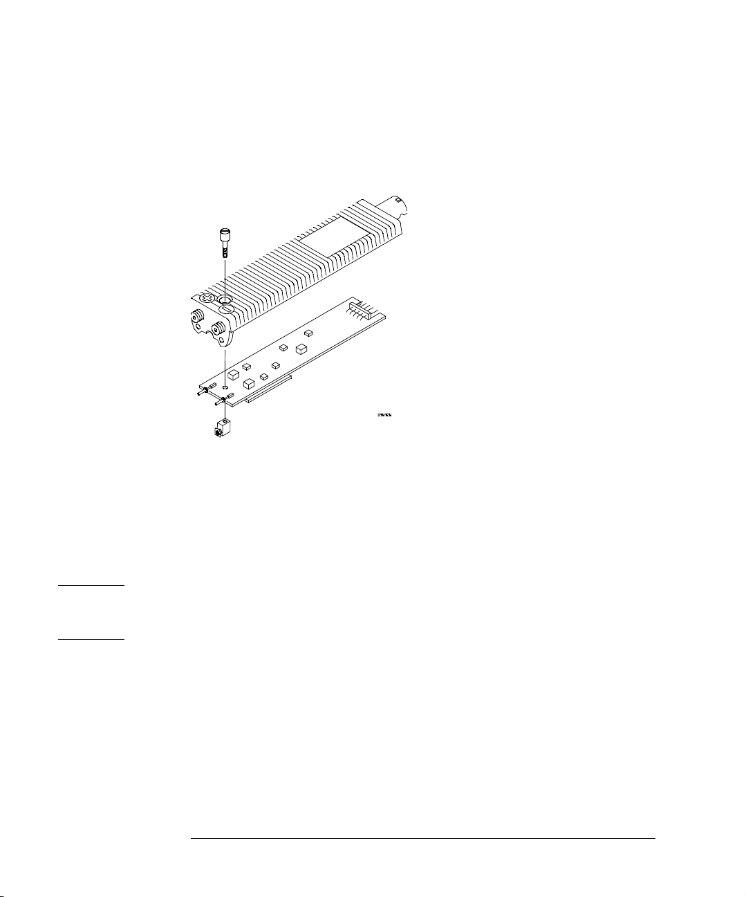
Figure 2-22
Calibration Tests and Adjustment
Adjustment Procedure
4 Assemble the PC assembly in the top cover.
The side of the PC assembly with the large hybrid is exposed when the assembly is in
the top cover. The figure below shows how the top cover, PC board, and ground block
fit together.
Reassembling the Probe
a
Insert the input connectors first, and seat the cable end of the PC assembly over the
pins at the rear of the cover.
b Position the ground block at the center-front of the PC assembly.
c Insert the grounding screw through the top cover and PC assembly and screw it into
the ground block as shown.
5 Replace the bottom cover.
a Position the cable strain relief and with one hand, hold the cable and top together.
The flange on the strain relief has a notch that fits around a protrusion in the top cover.
CAUTION Note where the two pins at the rear of the top cover enter the holes in the PC assembly.
Position the cable wires away from these two areas. Otherwise, when the bottom cover
is closed, part of it will pinch wires that are laying over these areas.
b Insert the pins at the front of the bottom cover into the holes at the front of the top
cover.
c Close the two covers together and fasten with the probe clamp ring.
48
Page 49

Calibration Tests and Adjustment
Attenuator Adapter Adjustment
Attenuator Adapter Adjustment
The following procedure should be used if it is necessary to adjust an attenuator adapter.
Attenuator adapters have only characteristics; they do not have any specifications. An
adapter will need adjustment only if one or more of the following occurs.
• If an adapter is to be used on a different 1141A probe that it was calibrated with
last.
• If an adapter needs to be optimized to requirements for a special measurement.
• If an adapter is suspected of needing adjustment.
NOTE Attenuator adapters should not be adjusted as part of routine maintenance. The design
necessary to give the high CMRR and high impedance of the attenuators makes
adjustment delicate.
Additionally, because of broadband noise, a spectrum analyzer should be used to verify
adjustment quality.
Each attenuator contains two identical voltage dividers on a ceramic substrate. There
are three adjustments. The low-frequency CMRR adjust the low-frequency balance
between the two voltage dividers. The two high-frequency adjustments are electrically
identical. Each adjusts the high-frequency compensation of one of the voltage dividers.
To meet both pulse response and CMRR characteristics they are adjusted differently.
Briefly, the adjustment procedure is:
a Adjust the positive high-frequency response (+ HF RESP) for the best pulse response
using a 3.5 kHz square wave.
b Adjust the negative high-frequency response (-HF RESP) and Low-frequency CMRR
(LF CMRR) for best CMRR using a 3.5 kHz square wave.
The following equipment is required for this procedure. Procedures are based on the
model or part number recommended.
Equipment Required
Equipment Required Critical Specifications Recommended
Function Generator 3.5 kHz, 3 V to 16 V
Oscilloscope 100 MHz at 1 mV/div 54830B
Probe/Power Module No substitute 1141A/1142A
Test Board No substitute 01141-66504
Cable BNC, 50 Ω 9-inch 10502A
Cable BNC, 50 Ω 36-inch 10503A
Alignment tool Flat blade (supplied accessory) 8710-1961/
p-p
Model/Part
33120A
Sprague-Goodman
part, GTT-5G
49
Page 50

Calibration Tests and Adjustment
Attenuator Adapter Adjustment
Adjustment Procedure
NOTE The attenuator must be adjusted when installed on the 1141A probe with which it will
be used. The specifications and characteristics will not be met if the attenuator adapter
is adjusted with one differential probe then used with another.
1 Remove the probe pins from the attenuator adapter and differential probe, then
attach the adapter to the probe.
2 Set the 1142A front panel switches to Local and Zero offset.
3 Use the 9-inch BNC cable to connect the function generator to the test board.
The short cable minimized ground-loop voltages.
4 Set up the function generator.
• Square wave
• 3.5 kHz
• 3.0 Vp-p for 10x adapter and 16 V
Use the long BNC cable to connect the Trig Out of the function generator to
5
for a 100x adapter.
p-p
the EXT TRIG of the oscilloscope.
6 Set up the oscilloscope, then set the following parameters.
Menu Selection Setting
TIMEBASE (time/div) 50 µs/div
CHAN 1 (sensitivity)
(input R)
TRIG (mode)
source
level
ACQUISITION Sampling Mode
Memory Depth
Sample Rate
Averaging
# of avg
50 mV/div
50 Ω DC
trg’d
EXT
1.00000 V
Real Time
Automatic
Automatic
Enabled
32
50
Page 51

Figure 2-23
Figure 2-24
Calibration Tests and Adjustment
Attenuator Adapter Adjustment
7 Connect the adapter/probe combination to the test board in the position shown
in the figure below.
Signal to + input
8 Adjust the + HF RESP for best overall pulse response, the flattest pulse top.
Use the figure below for adjust locations.
Adjustment Locations
9 Change the function generator to 10 V
10 On the oscilloscope, press CHAN and set the sensitivity to 1 mV/div.
(10x adapter adjustment only).
p-p
51
Page 52

Figure 2-25
Calibration Tests and Adjustment
Attenuator Adapter Adjustment
11 Connect the adapter/probe combination to the test board in the position shown
in the figure below (signal to both inputs).
Signal to both input
12 Alternately adjust the LF CMRR and then the -HF RESP for a minimum signal
on the oscilloscope. Repeat the adjustments until the signal is optimized to a
minimum. Each adjustment should be set to minimize the component of the
signal it affects most. Some high-frequency components of the signal are not
affected by either adjustment.
52
Page 53

3
Service
53
Page 54

Service
Introduction
Introduction
This section provides troubleshooting, service, and repair information for the
1141A Differential Probe and 1142A Probe Control and Power Module. The
troubleshooting information is provided to isolate a faulty assembly. When a
faulty assembly has been located, the disassembly/assembly procedures help
direct replacement of the assembly.
WARNING Maintenance should be performed by trained service personnel aware of the hazards
involved (for example, fire and electric shock). When maintenance can be performed
without power applied, the power cord must be removed from the instrument.
54
Page 55

Performance Specifications and Characteristics
Performance Specifications and Characteristics
The following table gives performance specifications used to test the 1141A and 1142A.
It also gives performance characteristics that are typical for the probe system.
Performance Specifications and Characteristics
Parameter Probe alone With 10x attenuator With 100x attenuator
SPECIFICATIONS
±20 Vdc
±0.5 V
1 MΩ
7 pF
rms
1
±200 Vdc, decreasing to
±3.0 mV at 30 Hz
±200 Vdc
linear change
±5 V
9 MΩ
3.5 pF
±500 Vdc, decreasing to
±30 mV at 30 Hz
±500 Vdc
linear change
±50 V
10 MΩ
2 pF
Bandwidth (-3 dB, dc coupled) dc to 200 MHz
Rise Time: (calculated) 1.75 ns
Gain Accuracy 2.0% 4.0%
CMRR See the graphs in figure 3-1
Maximum Input Voltage
(see figure 3-2)
Differential Input Range
DC mode with no offset ± 300 mV peak ±3.0 V peak ±30 V peak
with DC Reject or appropriate
offset
Common-mode Operating
Range
dc
dc to 30 Hz
30 Hz to 200 MHz
dc Offset Range ±20 V ±200 V ±500 V
Input Impedance Resistance
Capacitance
ac Low-freq. Response (-3dB) 15 Hz 1.5 Hz 1.5 Hz
dc Reject Response 5 Hz, 0.5 Hz, or 0.05 Hz (selectable irrespective of attenuator)
Output Impedance 50 Ω
Thermal drift ≤ 50 µVdc/°C
Displayed noises ≤ 50 µV
Overload Recovery < 1 ms from overdrive that is less than the common mode range
Note: 1. For maximum signal fidelity above 100 MHz, limit the probe input (without attenuators to ≤ 300 mV
peak-to-peak.
±200 V(dc + peak ac) ±500 V(dc + peak ac)
±20 Vdc, decreasing to
±300 mV at 30 Hz
linear change
Service
55
Page 56

Figure 3-1
Service
Performance Specifications and Characteristics
CMRR Specifications and Characteristics
Legend
A. CMRR specification for probe with no input adapters.
B. Low-frequency CMRR specification for probe with the ac adapter.
C. Typical CMRR characteristic for differential probe with no input adapters
D. Typical CMRR characteristic for differential probe with 100x attenuator adapter at input.
E. Typical CMRR characteristic for differential probe with 100x attenuator adapter at input.
56
Page 57

Figure 3-2
Maximum Input Voltage vs. Frequency
Legend
A. Input voltage limits for probe alone.
B. Input voltage limits for 10x adapter.
C. Input voltage limits for 100x adapter.
Service
Performance Specifications and Characteristics
57
Page 58

Service
General Characteristics
General Characteristics
The following characteristics apply to the 1141A Differential Probe with the 1142A Probe
Control and Power Module.
Environmental Conditions
Operating Non-operating
Temperature 0°C to +55 C° (32°F to +131°F) -40°C to +70°C (-40°F to +158°F)
Humidity up to 95% relative humidity (non-
condensing) at +40°C (+104°F)
Altitude up to 4,600 meters (15,000 ft) up to 15,300 meters (50,000 ft)
up to 90% relative humidity at +65°C
(+149°F)
Figure 3-3
Vibration Random vibration 5 to 500 Hz, 10
Power
Requirements
Weight Net: approximately 1.8 kg (4.0 lb.)
Dimensions Refer to the outline drawings below.
1142A Probe Control
and Power Module
minutes per axis, 0.3grms.
Voltage: 90 to 132/198 to 264 Vac, 47 to 440 Hz
Power: 25 VA maximum
Shipping: approximately 2.7 kg (6.0 lb.)
Random vibration 5 to 500 Hz, 10 min.
per axis, 2.41 grams. Resonant search
5 to 500 Hz swept sine, 1Octave/min.
sweep rate, (0.75g), 5 min. resonant
dwell at 4 resonances per axis.
1141A Differential
Probe
Mechanical Dimensions
58
Page 59

Figure 3-4
Service
Theory of Operation
Theory of Operation
The following discussion covers block-level theory for the 1141A/1142A differential
probe system. Refer to the block diagram below.
The differential probe system consists of two units, the 1141A Differential Probe with
its accessories and the 1142A Probe Control and Power Module. For purposes of the
following discussion, these will be called the probe and the control module respectively.
Differential Probe System Block Diagram
59
Page 60

Service
Theory of Operation
Differential Probe
The probe contains a two-path differential amplifier with unity gain. It is implemented
on a double-sided surface-mount PC board with the high-frequency path on one side and
the low-frequency path on the other. The two paths are split directly after the differential
input connections.
High-Frequency Path
The positive and negative inputs are ac-coupled at 33 Hz into identical impedance
converters. The HF CMRR adjustment balances the gain at the outputs of the impedance
converters. The impedance feed a semi-custom differential amplifier. An additional
negative input to the differential amplifier brings in the sum of the low-frequency and
feedback signals. The FREQ COMP adjustment provides variable high-frequency peaking
of the differential amp. The output amp provides two signals. A feedback signal is
summed with the low-frequency signals and the output signal is the final output of the
probe. Overall probe gain is set by the HIGH FREQ GAIN adjustment.
The entire signal portion of the high-frequency path is implemented on a hybrid IC.
Support circuitry includes bias for the impedance converters and a bias supply for
current sources on the hybrid.
Low-Frequency Path
The bandwidth of the low-frequency path is approximately 75 KHz. The positive and
negative inputs are dc coupled into identical inverting op-amps with gain of 0.5. They
provide a precision 1 M Ω input impedance for the probe. The LOW FREQ BANDWIDTH
adjustments match the gain and phase of the low-frequency path to that of the feedback
from the probe output. One of the two adjustments is set to match the properties of the
feedback and the other is to match the two low-frequency paths. These adjustments
affect the CMRR quality of the probe. The inputs of the inverting op-amps include
protection for ESD and over-voltage conditions.
The inverting op-amps feed a precision differential amplifier with unity gain and a singleended output. The output is fed to the summing amp and to the control module for use
in the dc reject circuit.
Summing Amp
The summing amp combines the feedback signal, the low-frequency signal, and the offset
signal. The LOW FREQ GAIN adjustment matches the gain of the low-frequency path to
the overall gain.
Control and Power Module
The control and power module provides offset functions, local and remote control, and
power to the probe system.
60
Page 61
Service
Theory of Operation
Offset Functions
There are two offset functions developed in the control module: variable offset and dc
reject. A variable offset voltage with coarse and fine adjustments can be selected by the
front panel controls. The offset level is buffered by U8 and selected by multiplexer U3
as the input to offset amp U7. The output of the offset amp is summed with the lowfrequency signal and feedback which gives dc coupling in the probe. Front panel
screwdriver adjustment Offset Null zeros the dc output from the probe when the dc input
and offset are zero.
For dc Reject, an output from the low-frequency amplifier in the probe (LFSIG) is used
to develop a voltage used to null the dc component of the input signal. LFSIG is an input
to U6, an inverting amplifier and low-pass filter. Multiplexer U3 selects one of three
capacitors to set a roll-off frequency of 0.05, 0.5, or 5 Hz. The output of U6 is selected,
again by U3, as the input to the offset amp. When the output of the offset amp is summed
into the low frequency path, the result is cancellation of the dc component of the input
signal. Front panel screwdriver adjustment DC Reject Gain adjusts the gain of the dc
reject circuit.
Local and Remote Control
The front panel switch controls the dc reject and offset functions. It also selects remote
operation, which allows control through the rear panel remote input connector.
Power Supply
The supply provides ±6 V and ±15 V for the probe and analog control circuitry as well
as +5 V for the digital control circuitry.
Figure 3-5
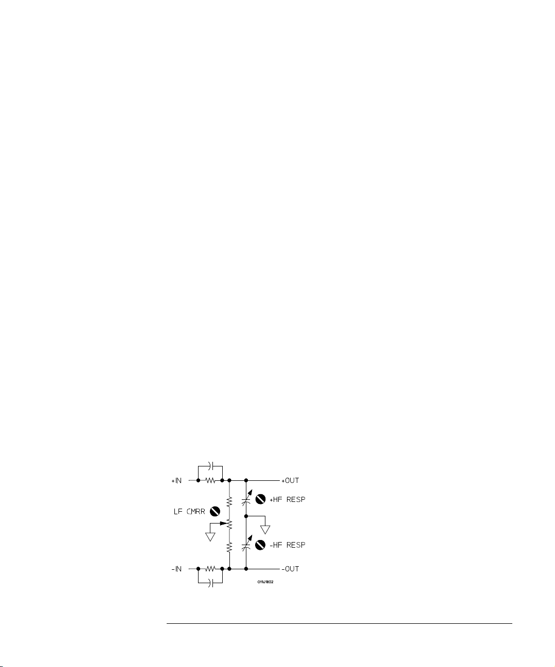
Attenuator Adapters
The 10x and 100x Attenuator Adapter are similar. A ceramic substrate carries two
attenuators, one for each input polarity. A variable resistor adjusts the low-frequency
balance (LF CMRR) between the two attenuators. The high-frequency adjustments are
the same for each attenuator. Each attenuator is adjusted differently. One attenuator is
adjusted for optimum pulse response and the other for best high-frequency CMRR.
Attenuator Adapter, Simplified Schematic
61
Page 62

Figure 3-6
Service
Theory of Operation
Test Board
The test board is a device for conveniently connecting test signals to the differential
probe. The probe can be connected to the board with the signal to the positive, negative,
or both inputs.
Test Board Schematic
62
Page 63

Service
Service Policy
Service Policy
For parts of the 1141A/1142A probe system that are complex, the service policy is for
assembly-level repair. For parts of the system with simple circuitry, the service policy is
component-level repair.
The service policy for the 1141A Differential Probe is assembly-level repair. Assemblies
include the PC assembly and cable. The PC assembly is an “exchange assembly.” A
repaired and tested assembly is shipped upon receipt of the defective assembly.
The attenuator and ac coupling adapters are shipped as complete assemblies.
The service policy for the 1142A Probe Control and Power Module is component-level
repair.
63
Page 64

Service
Troubleshooting
Troubleshooting
Use the following paragraphs to assist in troubleshooting problems with the 1141A/1142A
Differential Probe.
Probe Troubleshooting
To troubleshoot the probe:
Apply a known signal to the input of the probe.
1
2 Check for an identical output at the output coax to the cable. This connection
is the one soldered to the PC board. If the probe output cable is not terminated,
or the coax is open, the output signal will be about twice the amplitude of the
input signal.
3 If the signal is incorrect, check the power supply voltages from the 1142A Probe
Control and Power Module. Use the cable diagram on the next page.
4 Troubleshoot the cable with an ohmmeter. Use the cable diagram on the next
page.
Probe Control and Power Module Troubleshooting
The circuitry consists of simple power supplies, operational amplifiers, and TTL. Use
conventional troubleshooting techniques. A complete parts list, component locator, and
schematics are provided later in this chapter.
64
Page 65

Figure 3-7
Service
Troubleshooting
1142A Probe Control and Power Module
65
Page 66

Service
Removing and Replacing Assemblies
Removing and Replacing Assemblies
This section contains procedures for the removal and replacement of major assemblies.
CAUTION Never remove or install any assembly with the instrument power ON. Component
damage can occur.
Differential Probe
Use the following procedure to remove and replace the amplifier PC board in the
differential probe.
CAUTION ELECTROSTATIC DISCHARGE can damage electronic components. Use grounded
wrist straps and mats when servicing the probe.
CAUTION Handle the differential probe carefully once it has been disassembled. If unsupported,
the weight of the cable can put strain on the PC board.
Disassemble Probe
Remove the probe tip caps and probe tips.
1
2 Loosen the probe clamp ring at the cable end of the probe (1/4 turn counter-
clockwise) and slide it down the cable.
3 Remove the bottom cover.
a At the cable end of the probe, separate the covers about one centimeter (1/2 inch).
b Slide the bottom cover toward the cable end of the probe until the locator pins at
the probe input clear the holes. Then, remove the cover.
Note the way the cable strain relief is keyed and held at the rear of the top cover.
Remove the probe top cover.
4
The ground screw passes through the top cover and PC board and screws into the ground
block.
a Remove the ground screw on the top of the probe.
At the cable end, the PC board fits over the pins in the top cover.
b Lift the board off of the pins and slide it in the direction of the cable until the input
connectors clear the front of the probe.
5 Un-solder the two connections where the coaxial output cable connects to the
PC board.
6 Disconnect the cable connector from the probe PC board.
66
Page 67

Figure 3-8
Service
Removing and Replacing Assemblies
Reassemble Probe
The ground screw passes through the top cover and PC board and screws into the ground
block.
1
If replacing the PC board, remove the input connectors from the old board and
put them on the new one.
2 If replacing the cable, note the orientation of the probe clamp ring on the old
cable, remove the ring and put it on the new cable.
3 Connect the cable connector to the PC board.
4 Solder the two connections of the coaxial cable to the PC board.
On a new probe cable, the conductors of the coaxial cable are connected by a heavy
single wire. Cut the heavy wire so it matches the wire on the cable that was removed.
5 Assemble the PC assembly into the top cover.
The large hybrid is exposed when the assembly is in the top cover. The figure on the
below shows the sequence of the ground screw, top cover, PC board, and ground block.
Reassembling the Probe
a
Insert the input connectors first, and seat the cable end of the PC assembly over the
pins at the rear of the cover.
b Position the ground block at the front of the PC assembly.
c Insert the grounding screw through the top cover and screw it into the ground block
as shown in the figure above.
6 Replace the bottom cover.
a Position the cable strain relief and with one hand, hold the cable and top cover
together.
The flange on the strain relief has a notch that fits over a protrusion in the top cover.
67
Page 68

Service
Removing and Replacing Assemblies
CAUTION Note where the two pins at the rear of the top cover enter the holes in the PC assembly.
Position the cable wires away from these two areas. When the bottom cover is closed,
part of it will pinch wires that are laying over these areas.
b Insert the pins at the front of the bottom cover into the holes at the front of the top
cover.
c Close the covers together and fasten with the probe clamp ring. If the covers do not
fit together tightly and easily, check for pinched wires (see caution above).
Probe Adapters
Use the following procedure to disassemble the probe adapters. The adapter housing
consists of two plastic parts, one of which slides into the other. The parts are held
together by the spring effect of two plastic tabs on the inner part.
Mechanically, the ac adapter is about the same as the 10x and 100x attenuator adapters.
The attenuator adapters have an extra ground connector which connects the substrate
ground to the thumbwheel screw and plating inside the housing.
Disassemble Adapter
Remove the probe tip caps and probe tips from the adapter input.
1
2 Hold the adapter in one hand taking care not to block the output end of the
adapter (the end which attaches to the probe).
3 Note the view of the input end of the adapter in the figure below. The arrows
indicate the holding tabs.
Figure 3-9
Disassembling Adapters
4 With the thumb and forefinger, squeeze the tabs together, as indicated by the
arrows. Simultaneously, push the tabs into the outer housing so the inner
housing begins to slide out.
5 While holding the outer housing, push back against the thumbwheel until the
inner housing can be grasped and removed.
Reassemble Adapter
Reassembling the adapter is slightly harder because you have to align the connector pins
and thumbwheel screw, while sliding the inner housing and outer housing together.
1
Be sure the input connectors and output pins are present and seated on the
substrate or PC board.
68
Page 69

Figure 3-10
Service
Removing and Replacing Assemblies
2 Combine the thumbwheel screw and thumbwheel and insert them into the hole
in the outer housing.
3 Insert the substrate/board into the outer housing. Slip the attenuator ground
(attenuator adapters only) over the thumbwheel screw and seat the input
connectors in the proper holes in the housing.
Reassembling the Adapter
Do not force reassembly of the adapter. The housing halves will slide together with
moderate friction.
4 Align the inner housing tabs with the grooves in the side of the outer housing
and slide the two partly together.
While seating the thumbwheel screw and pins, it will help to hold the assembly vertically,
with the input end of the adapter down. This will allow the assemblies to sit vertically
and more easily align with the holes in the inner housing.
5
Seat the thumbwheel screw first, then the output pins, into the appropriate
holes in the inner housing.
6 Once the two housings are nearly together, press them together firmly until
the tabs click into place.
69
Page 70

Service
Removing and Replacing Assemblies
Probe Control and Power Module
Use the following procedure to disassemble the probe control and power module.
WARNING Hazardous voltages exist on the power supply. To avoid electrical shock, adhere closely
to the following procedures.
1 Remove the power cord.
2 Remove four flathead screws and remove the top cover.
WARNING Be sure to reconnect the safety ground when reassembling the instrument.
3 Unplug the safety ground from the tab on the rear panel of the instrument.
4 Note the orientation of the knobs. Remove the two knobs.
5 On the bottom of the instrument, remove the 5mm screw that fastens the
transformer support.
6 Remove the following pan-head screws.
• Three directly on the PC board.
• Two on the ac input connector.
• Two on the heatsink.
7
Remove the PC board. Slide it slightly forward so parts will clear the rear panel,
then lift the rear of the board out while sliding it backwards.
8 Remove the two heatsink spacers from the standoffs that were directly under
the heatsink.
9 Reverse the procedure to reassemble the control and power supply.
70
Page 71

Service
Replaceable Parts
Replaceable Parts
This section contains information for ordering parts. Service support for the 1141A
Differential Probe is to the assembly level. Service support for the adapters is as complete
assemblies, except for the probe tip caps and the probe tips. Service support for the
1142A Probe Control and Power Module is to the component level.
Parts List
The replaceable parts lists include all parts relevant to the applicable service levels. The
information given for each part consists of the following:
• Reference designator
•Part number
• Total quantity (Qty) in instrument or on assembly. The total quantity is given once
and at the first appearance of the part number in the list.
• Description of part
• Typical manufacturer of part in a five-digit code.
Ordering Information
To order a part in the material part list, quote the part number, indicate the quantity
desired, and address the order to the nearest Agilent Technologies Sales Office.
To order a part not listed in the material list, include the instrument part number,
instrument serial number, a description of the part (including its function), and the
number of parts required. Address the order to the nearest Agilent Technologies Sales
Office.
Direct Mail Order System
Within the USA, Agilent Technologies can supply parts through a direct mail order
system. There are several advantages to this system:
• Direct ordering and shipment from the Agilent Technologies parts center in
California, USA.
• No maximum or minimum on any mail order (there is a minimum amount for parts
ordered through a local Agilent Technologies Sale Office when the orders require
billing and invoicing).
• Prepaid transportation (there is a small handling charge for each order).
• No invoices.
In order for Agilent Technologies to provide these advantages, a check or money order
must accompany each order.
71
Page 72

Service
Replaceable Parts
Mail order forms and specific ordering information are available through your local
Agilent Technologies Sales Office. Addresses and telephone numbers are located in a
separate document shipped with the manuals.
Manufacturers’ Codes
A list of manufacturers’ codes is given the table below. The codes are given for parts in
the parts lists. The table gives the manufacturer and address for each code.
Manufacturers’ Code List
Mfr. No. Name Address
00000 Any satisfactory supplier
06665 Precision Monolithics Inc. Santa Clara, CA 95050
24546 Corning Glass Works (Bradford) Bradford, PA 16701
27014 National Semiconductor Corp Palo Alto, CA 94304
28480 Agilent Technologies Corporate Hq Palo Alto, CA 94304
32997 Bourns Inc. Riverside, CA 92507
72
Page 73

Figure 3-11
Service
Replaceable Parts
Exploded View
1141A Differential Probe Parts
73
Page 74

Figure 3-12
Service
Replaceable Parts
Power and Control Board Component Locator
74
Page 75

Figure 3-13
Service
Replaceable Parts
Cabling Diagram
75
Page 76
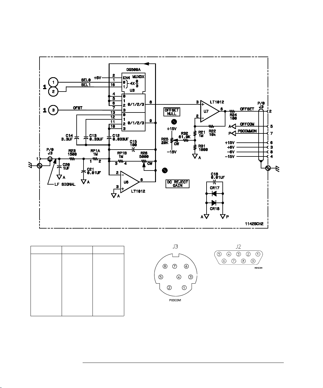
Figure 3-14
Service
Replaceable Parts
IC Connectors not Shown
Supply Pin No. IC Group
+15 14 U3
-15 3
GND 15
+15 7 U6-8, 11
-15 4
NC 1, 5, 8
+5 16 U9
GND 8
1142A Probe Control and Power Module
76
Page 77

Figure 3-15
Service
Replaceable Parts
1142A Probe Control and Power Module
77
Page 78

Service
Replaceable Parts
1141A and 1142A Replaceable Parts
Ref.
Des.
A1 01141-66503 1 PC ASSEMBLY-DIFFERENTIAL PROBE 28480 01141-66501
E1 01141-26102 2 PROBING PIN 28480 01141-26102
E2 01141-22301 1 GROUND BLACK 28480 01141-22301
E3 01141-22401 1 GROUND SCREW 28480 01141-22401
MP1 01141-24102 2 CAP-PROBING PIN 28480 01141-24101
MP2 01141-44702 1 PROBE BOTTOM COVER 28480 01141-44701
MP3 01141-44102 1 PROBE TOP COVER 28480 01141-44101
MP4 01141-22502 1 PROBE POS CLAMP RING 28480 01141-22501
MP5 01141-94307 1 DIFFERENTIAL PROBE LABEL 28480 01141-94301
W1 01141-61603 1 PROBE CABLE ASSEMBLY 28480 01141-61601
Part
Number
01141-26102 2 PROBING PIN 28480 01141-26102
01141-24102 2 CAP-PROBING PIN 28480 01141-24101
Qty Description Mfr.
Code
1141A Differential Probe
10X Attenuator Adapter
Mfr. Part
Number
100X Attenuator Adapter
01141-26102 2 PROBING PIN 28480 01141-26102
01141-24102 2 CAP-PROBING PIN 28480 01141-24101
AC Adapter
01141-26102 2 PROBING PIN 28480 01141-26102
01141-24102 2 CAP-PROBING PIN 28480 01141-24101
1142A PROBE CONTROL AND POWER MODULE
78
Page 79

1141A and 1142A Replaceable Parts
Service
Replaceable Parts
Ref.
Des.
A1 01142-66501 1 PC ASSEMBLY-POWER AND CONTROL 28480 01142-66501
H1 0515-0374 7 SCREW-MACHINE M3 10mm-LG 00000 ORDER BY DESP.
H2 0515-1031 4 SCREW-MACHINE M3 6mm-LG 90-DEG-FLH-HD 00000 ORDER BY DESP.
H3 0515-1579 1 SCREW-MACHINE M5 18mm-LG 00000 ORDER BY DESP.
MP1 01142-47702 1 BOTTOM CHASSIS 28480 01142-47701
MP2 01142-44101 1 TOP CHASSIS 28480 01142-44101
MP3 01142-24701 2 SPACER-HEAT SINK 28480 01142-24701
MP4 0370-1097 2 KNOB-POINTER 28480 0340-1097
MP5 0403-1012 4 FOOT 28480 0403-0727
MP6 5041-0234 5 KEYCAP 28480 5041-0234
W1 8120-1521 1 POWER CORD 18-AWG 3-COND 90-IN-LG (US/
Part
Number
Qty Description Mfr.
Code
28480 8120-1521
Canada only)
Mfr. Part
Number
79
Page 80

Service
Replaceable Parts
Power Supply Replaceable Parts
Ref. Des. Part
Number
C1 0160-6190 2 CAPACITOR-FXD 0.33UF ±10% 50VDC 28480 0160-6190
C2 0160-5474 1 CAPACITOR-FXD 0.1UF ±5% 100VDC MET-POLY 28480 0160-5474
C3 0180-3298 2 CAPACITOR-FXD 2200UF+30-10% 50VDC AL 28480 0180-3298
C4 0180-3298 CAPACITOR-FXD 2200UF+30-10% 50VDC AL 28480 0180-3298
C5 0160-6500 4 CAPACITOR-FXD 0.01UF ±10% 100VDC CER 28480 0160-6500
C6 0160-6500 CAPACITOR-FXD 0.01UF ±10% 100VDC CER 28480 0160-6500
C7 0160-6500 CAPACITOR-FXD 0.01UF ±10% 100VDC CER 28480 0160-6500
C8 0160-6500 CAPACITOR-FXD 0.01UF ±10% 100VDC CER 28480 0160-6500
C9 0180-3845 4 CAPACITOR-FXD 4.7UF ±10% 35VDC TA 28480 0180-3845
C10 0180-3845 CAPACITOR-FXD 4.7UF ±10% 35VDC TA 28480 0180-3845
C11 NOT ASSIGNED
C12 0160-5581 1 CAPACITOR-FXD 0.033UF ±10% 63VDC 28480 0160-5581
C13 0160-6190 CAPACITOR-FXD 0.33UF ±10% 50VDC 28480 0160-6190
C14 0160-7060 1 CAPACITOR-FXD 3.3UF ±10% 63VDC 28480 0160-7060
C15 0160-4801 1 CAPACITOR-FXD 100PF ±5% 100VDC CER 28480 0160-4801
Qty Description Mfr.
Code
Prefix the reference designators with A1
Mfr. Part
Number
C16 0180-3845 CAPACITOR-FXD 4.7UF ±10% 35VDC TA 28480 0180-3845
C17 0180-3845 CAPACITOR-FXD 3.3UF ±10% 63VDC 28480 0180-3845
C18 NOT ASSIGNED
C19 0160-5471 1 CAPACITOR-FXD 0.1UF ±5% 50VDC MET-POLY 28480 0160-5471
C20 0160-5469 1 CAPACITOR-FXD 1UF ±10% 50VDC MET-POLY 28480 0160-5469
C21-22 NOT ASSIGNED
C23 0180-3784 4 CAPACITOR-FXD 22UF ±20% 25VDC TA 28480 0180-3784
C24 0180-3784 CAPACITOR-FXD 22UF ±20% 25VDC TA 28480 0180-3784
C25 0180-3784 CAPACITOR-FXD 22UF ±20% 25VDC TA 28480 0180-3784
C26 0180-3784 CAPACITOR-FXD 22UF ±20% 25VDC TA 28480 0180-3784
80
Page 81

Power Supply Replaceable Parts
Service
Replaceable Parts
Ref. Des. Part
Number
CR1 NOT ASSIGNED
CR2 1901-1087 2 DIODE-PWR RECT 100V 3A 04713 MR501
CR3 1901-1087 DIODE-PWR RECT 100V 3A 04713 MR501
CR4 NOT ASSIGNED
CR5 1901-0731 8 DIODE-PWR RECT 400V 1A 28480 1901-0731
CR6 1901-0731 8 DIODE-PWR RECT 400V 1A 28480 1901-0731
CR7-8 NOT ASSIGNED
CR9 1901-0731 8 DIODE-PWR RECT 400V 1A 28480 1901-0731
CR10 1901-0731 8 DIODE-PWR RECT 400V 1A 28480 1901-0731
CR11 1901-0731 8 DIODE-PWR RECT 400V 1A 28480 1901-0731
CR12 1901-0731 8 DIODE-PWR RECT 400V 1A 28480 1901-0731
CR13 1901-0734 2 DIODE-PWR RECT 1N5818 30V 1A 04713 IN5818
CR14 1901-0734 2 DIODE-PWR RECT 1N5818 30V 1A 04713 IN5818
CR15-16 NOT ASSIGNED
CR17 1901-0731 DIODE-PWR RECT 400V 1A 28480 1901-0731
CR18 1901-0731 DIODE-PWR RECT 400V 1A 28480 1901-0731
Qty Description Mfr.
Code
Mfr. Part
Number
DS1 1990-0521 1 LED-LAMP LUM-INT=2.2MCD IF=50MA-MAX 24840 5082-4955
E1 2110-0642 1 FUSEHOLDER 6.3A 250A 28480 2110-0642
E2 2110-0565 1 FUSEHOLDER CAP 28480 2110-0565
F1 2110-0201 1 FUSE 0.25A 250V TD 28480 2110-0201
H1 0515-1579 1 SCREW-MACHINE M5 18mm-LG 28480 0515-1579
HS1 01142-21101 1 HEAT SINK 28480 01142-21101
81
Page 82

Service
Replaceable Parts
Power Supply Replaceable Parts
Ref. Des. Part
Number
J1 1252-4731 1 CONNECTOR-AC PWR 28480 1251-4743
J2 1252-1487 1 CONN-RECT D-SUBMIN 9-CKT (remote) 28480 1252-1487
J3 1252-3935 1 CONNECTOR-ROUND 8-CKT (probe) 28480 1252-3134
MP1 1400-1604 1 LED MOUNT 28480 1400-1604
MP2 1205-0732 4 SPRING CLIP 28480 1205-0732
MP3 0361-0685 3 RIVET-BLIND DR-PIN RNDH 0.125DIA 28480 0361-0685
MP4 0340-1211 3 INSULATOR-THERMAL 28480 0340-1211
MP5-6 NOT ASSIGNED
MP7 1400-0249 1 CABLE TIE 0.062-0.625-DIA 0.091-WD NYL 16956 08-465/GRY
MP8 01142-24702 1 TRANSFORMER SUPPORT 28480 01142-24702
MP9 01142-28801 1 WASHER-TRANSFORMER SUPPORT 28480 01142-28801
R1-2 NOT ASSIGNED
R3 0757-0442 4 RESISTOR 10K 1% 0.125W TF TC=0±100 24546 CT4-1/8-TO-1002-F
R4 0757-0465 1 RESISTOR 100K 1% 0.125W TF TC=0±100 24546 CT4-1/8-TO-1003-F
R5 0757-0199 5 RESISTOR 21.5K 1% 0.125W TC=0±100 24546 CT4-1/8-TO-2152-F
R6 0757-0199 RESISTOR 21.5K 1% 0.125W TC=0±100 24546 CT4-1/8-TO-2152-F
Qty Description Mfr.
Code
Mfr. Part
Number
R7 0698-4431 2 RESISTOR 2.05K 1% 0.125W TF TC=0±100 24546 CT4-1/8-TO-2052-F
R8 0699-1203 4 RESISTOR 120.0 1% 0.125W TF TC=0±25 28480 0699-1203
R9 0757-0434 2 RESISTOR 3.65K 1% 0.125W TF TC=±100 24546 CT4-1/8-TO-3651-F
R10 0698-4431 RESISTOR 2.05K 1% 0.125W TF TC=0±100 24546 CT4-1/8-TO-2052-F
R11 0699-1203 RESISTOR 120.0 1% 0.125W TF TC=0±25 28480 0699-1203
R12 0757-0434 RESISTOR 3.65K 1% 0.125W TF TC=0±100 24546 CT4-1/8-TO-3651-F
R13 0757-0420 1 RESISTOR 750 1% 0.125W TF TC=0±100 24546 CT4-1/8-TO-751-F
R14 0698-4002 2 RESISTOR 5K 1% 0.125W TF TC=0±100 24546 CT4-1/8-TO-5001-F
R15 0699-1203 RESISTOR 120.0 1% 0.125W TF TC=0±25 28480 0699-1203
82
Page 83

Power Supply Replaceable Parts
Service
Replaceable Parts
Ref. Des. Part
Number
R16 0698-6317 2 RESISTOR 500 0.1% 0.125W TF TC=0±25 28480 0698-6317
R17 0698-4002 RESISTOR 5K 1% 0.125W TF TC=0±100 24546 CT4-1/8-TO-5001-F
R18 0699-1203 RESISTOR 120.0 1% 0.125W TF TC=0±25 28480 0699-1203
R19 0698-6317 RESISTOR 500 0.1% 0.125W TF TC=0±25 28480 0698-6317
R20 NOT ASSIGNED
R21 0698-8827 1 RESISTOR 1M 1% 0.125W TF TC=0±100 28480 0698-8827
R22 0757-0442 RESISTOR 10K 1% 0.125W TF TC=0±100 24546 CT4-1/8-TO-1002-F
R23 0757-0427 1 RESISTOR 1.5K 1% 0.125W TF TC=0±100 24546 CT4-1/8-TO-1501-F
R24 0757-0401 1 RESISTOR 100 1% 0.125W TF TC=0±100 24546 CT4-1/8-TO-101-F
R25 2100-3161 1 RESISTOR-TRMR 20K 10% TKF SIDE-ADJ 32997 3006P-1-203
R26 2100-3056 1 RESISTOR-TRMR 5K 10% TKF SIDE-ADJ 17-TRN 32997 3006P-1-502
R27 0757-0199 RESISTOR 21.5K 1% 0.125W TF TC=0±100 24546 CT4-1/8-TO-2152-F
R28 0757-0199 RESISTOR 21.5K 1% 0.125W TF TC=0±100 24546 CT4-1/8-TO-2152-F
R29 0757-0442 RESISTOR 10K 1% 0.125W TF TC=0±100 24546 CT4-1/8-TO-1002-F
R30 0757-0442 RESISTOR 10K 1% 0.125W TF TC=0±100 24546 CT4-1/8-TO-1002-F
R30 0757-0280 1 RESISTOR 1K 1% 0.125W TF TC=0±100 24546 CT4-1/8-TO-1001-F
R32 0757-0460 1 RESISTOR 61.9K 1% 0.125W TF TC=0±100 24546 CT4-1/8-TO-6192-F
R33-39 NOT ASSIGNED
Qty Description Mfr.
Code
Mfr. Part
Number
R40 0757-0123 1 RESISTOR 34.8K 1% 0.125W TF TC=0±100 28480 0757-0123
R41 2100-4250 2 RESISTOR-VAR 10K 20% 28480 2100-4250
R42 2100-4250 RESISTOR-VAR 10K 20% 28480 2100-4250
R43 0757-0458 1 RESISTOR 51.1K 1% 0.125W TF TC=0±100 24546 CT4-1/8-TO-5112-F
R44 0683-2755 1 RESISTOR 2.7M 1% 0.25W TF TC=0±100 28480 0683-2755
R45 0698-4517 1 RESISTOR 127K 1% 0.125W TF TC=0±100 24546 CT4-1/8-TO-1273-F
R46 0698-3271 1 RESISTOR 115K 1% 0.125W TF TC=0±100 24546 CT4-1/8-TO-1153-F
R47 0698-8961 1 RESISTOR 909K 1% 0.125W TF TC=0±100 28480 0698-8961
R48 0757-0199 RESISTOR 21.5K 1% 0.125W TF TC=0±100 24546 CT4-1/8-TO-2152-F
83
Page 84

Service
Replaceable Parts
Power Supply Replaceable Parts
Ref. Des. Part
Number
RP1 1810-1242 1 RESISTOR NETWORK 28480 1810-1242
S1 3101-2609 1 SWITCH-SL DPST STD 5A 250VAC PC 28480 3101-2609
S2 3101-3007 1 SWITCH-6 STATION ASSEMBLY 28480 3101-3007
T1 9100-4750 1 TRANSFORMER-POWER (with mtg. hardware) 28480 9100-4750
U1 1826-1403 2 IC V RGLTER-ADJ-POS 3/40V 00000 LT317AT
U2 1826-1670 2 IC V RGLTR-ADJ-NEG -37/1.2V TO-220 PKG 00000 LT337AT
U3 5081-9233 1 ANALOG MULTIPLEXER 4 CHNL 16 -DIP-P 28480 1820-2182
U4 1826-1403 IC V RGLTR ADJ-POS 3/40V 00000 LT317AT
U5 1826-1670 IC V RGLTR-ADJ-NEG -37/1.2V TO-220 PKG 00000 LT337AT
U6 1826-1381 3 IC OP AMP LOW-BIAS-H-IMPD 8-DIP-P PKG 00000 LT1012CN8
U7 1826-1381 IC OP AMP LOW-BIAS-H-IMPD 8-DIP-P PKG 00000 LT1012CN8
U8 1826-1381 IC OP AMP LOW-BIAS-H-IMPD 8-DIP-P PKG 00000 LT1012CN8
U9 1820-3177 1 IC MUXR/DATA-SEL CMOS/74HC 2-TO-1-LINE 04713 MC74HC157N
U10 1826-0774 1 IC V RGLTR-V-REF-FXD 1.22/1.24V TO-92 27014 LM385BZ-1.2
U1 1826-0635 1 IC OP AMP LOW-OFS 8-DIP-P PKG 06665 OP-07CP
Qty Description Mfr.
Code
Mfr. Part
Number
VR1 1902-0951 1 DIODE-ZNR 5.1V 5% D0-35 PD=.4W TC±.035% 28480 1902-0951
W1 01141-61602 1 CABLE ASSEMBLY, SAFETY GROUND 28480 01141-61602
84
Page 85

Service
Replaceable Parts
Locator Table for Control and Power Supply
Ref.
Grid
Ref
Grid
Ref
Grid
Ref
Grid
Ref
Grid
Ref
Grid
Ref
Grid
Ref
Des.
Loc
Des
Loc
Des
Loc
Des
Loc
Des
Loc
Des
Loc
Des
Loc
C1 C-2 C17 C-6 CR10 C-5 J1 G-7 R5 B-6 R22 B-3 R45 C-3 U5 D-6
C2 F-3 C18 B-5 CR11 C-3 J2 B-7 R6 B-6 R23 B-5 R46 C-3 U6 B-3
C3 H-2 C19 B-6 CR12 C-6 J3 C-7 R7 C-4 R24 B-5 R47 C-2 U7 C-3
C4 J-3 C20 B-5 CR13 C-3 R8 C-5 R25 B-2 R48 D-3 U8 B-3
C5 C-3 C21 B-5 CR14 C-6 MP1 H-1 R9 C-4 R26 B-2 U9 A-5
C6 C-5 C22 B-6 CR17 B-5 MP2 E-3 R10 C-5 R27 A-5 RP1 B-3 U10 C-2
C7 B-3 C23 B-4 CR18 B-6 MP3 D-3 R11 C-5 R28 A-5 U11 C-3
C8 C-5 C24 B-6 MP4 E-5 R12 C-5 R29 B-6 S1 H-7
C9 C-5 C25 B-4 DS1 G-2 MP7 E-4 R13 E-3 R30 B-6 S2 E-2 VR1 E-3
C10 C-5 C26 G-6 MP8 G-4 R14 C-4 R31 B-3
C11 E-3 E1 F-6 MP9 G-4 R15 C-4 R32 B-2 T1 H-5
C12 A-3 CR2 F-3 E2 E-6 R16 C-4 R40 C-2
Grid
Des
Loc
C13A-3 CR3F-3 P1 E-7 R17A-2R41A-2U1 D-4
C14 B-4 CR5 C-3 F1 E-6 R18 C-6 R42 C-2 U2 D-5
C15 A-3 CR6 C-5 R3 A-6 R19 C-6 R43 C-2 U3 A-2
C16 C-4 CR9 C-3 HS1 D-5 R4 A-6 R21 B-3 R44 C-3 U4 D-3
85
Page 86

Service
Replaceable Parts
86
Page 87

Index
Numerics
100x attenuator test
10x attenuator test
A
ac adapter, 20
ac coupling adapters
ac low frequency
accessories
available to order
circuit connector posts
extension leads
ground leads
mini grabbers
probe tips
shielded signal leads
supplied with probe
test board
using
accuracy test, attenuator
adapter combinations
adapters
attenuator
adjustment
attenuator adapter
initial
probe
altitude
amplifiers
assemblies, removing & replacing
attenuator
adapter adjustment, 49
adapters
B
bandwidth
specification
test
blocking dc
block-level theory
, 14
, 26
, 13
, 16
, 61
, 11
, 13
, 40, 42
, 58
, 23
66
, 61
, 34
, 18
, 32
, 30
, 19
, 55
, 8
, 15
, 14
, 14
, 15
, 15
, 6
, 30, 32
, 17
, 49
, 55
, 59
C
cabling diagram, 75
calibration
test record, 39
tests
, 27
characteristics
environmental, 58
general
, 58
performance
probe connectors
circuit connector posts
cleaning instrument
CMRR
definition
high frequency gain
low frequency response
specification
, 36
test
common mode rejection ratio
compensating dc
component locator
power & control board, 74
connector
characteristics, 18
compatibility
control module
coupling functions
D
,
dc gain accuracy
dc mode
dc offset
dc reject
dc reject gain
differential amplifiers
differential input range
differential probe
disassembly
reassembly
dimensions
direct mail order parts
displayed noises, displayed
, 55
, 23
, 55
, 18
, 18
, 60
, 28
, 55
, 19, 55
, 19, 55
, 11
, 66
, 67
, 58
, 18
, 22
, 18
, 15
, 42
, 23
, 55
, 71
, 44
, 55
, 23
E
environmental characteristics
exchange assemblies
extension leads
F
features, 2
frequency
high compensation, 47
low response
function select
G
gain, 42
gain accuracy specification
general characteristics
ground leads
grounding
H
high frequency
compensation
gain &CMRR adjustment
high-frequency path
humidity
I
impedance, output, 55
initial adjustment
input impedance
input range, differential
input voltage, maximum
inspecting
L
line voltage
local control
locator table
low frequency response
low-frequency path
, 14
, 18
, 58
, 9
, 10
, 61
, 85
, 63
, 14
, 44
, 22
, 55
, 58
, 47
, 42
, 60
, 11
, 55
, 55
, 55
, 44
, 60
, 58
87
Page 88

Index
M
making measurements
manufacturer’s codes
maximum input voltage
mini grabbers
N
noises
O
offset, 20
offset functions
offset null
operating environment
operating range
ordering information
output impedance
overload recovery
P
parts list
performance specification
power module
disassembly
troubleshooting
power requirements
power supply
probe adapter
disassembly
reassembly
probe adjustment
probe control
disassembly
troubleshooting
probe gain test
probe tips
procedure
attenuator adjustment
bandwidth
CMRR test
probe adjustment
, 15
, 55
, 11
, 71, 78
, 60
, 70
, 61
, 68
, 68
, 70
, 14
, 34
, 36
, 13
, 72
, 55
, 61
, 58
, 55
, 71
, 55
, 55
, 64
, 10, 58
, 40
, 64
, 28
, 42
, 55
, 50
probe gain
probe preparation
R
recommended test equipment
record calibration
remote control
remote functions
remote input connection
remote offset input
remote operation
removing assemblies
replaceable parts
replaceable parts list
replacing assemblies
rise time, specification
S
schematic
probe & power module
probe control & power module
service policy
setting up probe
setup procedure
shielded signal leads
signal level
specifications, performance
summing amp
system preparation
T
temperature
test
100x attenuator accuracy
10x attenuator accuracy
bandwidth
calibration
CMRR
record calibration
test board
test equipment
, 28
, 41
, 39
, 61
, 22
, 21
, 22
, 21
, 66
, 71
, 78
, 66
, 55
, 65, 76
77
, 63
, 10
, 11, 12
, 15
, 18
, 55
, 60
, 10
, 58
, 32
, 30
, 34
, 27
, 36
, 39
, 18, 26, 62
, 9, 26
, 9
test procedures, calibration
test record, calibration
testing interval
theory of operation
thermal drift
troubleshooting
power module, 64
probe
probe control
U
using accessories, 13
using the probe
V
variable offset
vibration
W
weight, 58
,
, 55
, 64
, 22
, 58
, 27
, 27
, 27
, 59
, 64
, 9
88
Page 89

Notices
© Agilent Technologies, Inc.
2000-2004
No part of this manual may be
reproduced in any form or by any
means (including electronic
storage and retrieval or
translation into a foreign
language) without prior
agreement and written consent
from Agilent Technologies, Inc. as
governed by United States and
international copyright laws.
Manual Part Number
01141-97002, July 2004
Print History
01141-97000, June 2000
01141-97001, September 2002
01141-97002, July 2004
Agilent Technologies, Inc.
1900 Garden of the Gods Road
Colorado Springs, CO 80907 USA
Warranty
The material contained in this
document is provided “as is,” and
is subject to being changed,
without notice, in future editions.
Further, to the maximum extent
permitted by applicable law,
Agilent disclaims all warranties,
either express or implied, with
regard to this manual and any
information contained herein,
including but not limited to the
implied warranties of
merchantability and fitness for a
particular purpose. Agilent shall
not be liable for errors or for
incidental or consequential
damages in connection with the
furnishing, use, or performance
of this document or of any
information contained herein.
Should Agilent and the user have
a separate written agreement
with warranty terms covering the
material in this document that
conflict with these terms, the
warranty terms in the separate
agreement shall control.
Technology Licenses
The hardware and/or software
described in this document are
furnished under a license and
may be used or copied only in
accordance with the terms of
such license.
Restricted Rights
Legend
If software is for use in the
performance of a U.S.
Government prime contract or
subcontract, Software is delivered
and licensed as “Commercial
computer software” as defined in
DFAR 252.227-7014 (June 1995),
or as a “commercial item” as
defined in FAR 2.101(a) or as
“Restricted computer software”
as defined in FAR 52.227-19
(June 1987) or any equivalent
agency regulation or contract
clause. Use, duplication or
disclosure of Software is subject
to Agilent Technologies’ standard
commercial license terms, and
non-DOD Departments and
Agencies of the U.S. Government
will receive no greater than
Restricted Rights as defined in
FAR 52.227-19(c)(1-2) (June
1987). U.S. Government users will
receive no greater than Limited
Rights as defined in FAR 52.22714 (June 1987) or DFAR 252.2277015 (b)(2) (November 1995), as
applicable in any technical data.
Manual Safety Notices
CAUTION:
A CAUTION notice denotes a
hazard. It calls attention to an
operating procedure, practice, or
the like that, if not correctly
performed or adhered to, could
result in damage to the product or
loss of important data. Do not
proceed beyond a CAUTION
notice until the indicated
conditions are fully understood
and met.
WARNING:
A WARNING notice denotes a
hazard. It calls attention to an
operating procedure, practice, or
the like that, if not correctly
performed or adhered to, could
result in personal injury or death.
Do not proceed beyond a
WARNING notice until the
indicated conditions are fully
understood and met.
Agilent Technologies
P.O. Box 2197
1900 Garden of the Gods Road
Page 90

Product Safety
Notices
This apparatus has been designed
and tested in accordance with
IEC Publication 1010, Safety
Requirements for Measuring
Apparatus, and has been supplied
in a safe condition. This is a
Safety Class I instrument
(provided with terminal for
protective earthing). Before
applying power, verify that the
correct safety precautions are
taken (see the following
warnings). In addition, note the
external markings on the
instrument that are described
under "Safety Symbols."
Warnings
Before turning on the instrument,
you must connect the protective
earth terminal of the instrument
to the protective conductor of the
(mains) power cord. The mains
plug shall only be inserted in a
socket outlet provided with a
protective earth contact. You
must not negate the protective
action by using an extension cord
(power cable) without a
protective conductor
(grounding). Grounding one
conductor of a two-conductor
outlet is not sufficient protection.
Only fuses with the required rated
current, voltage, and specified
type (normal blow, time delay,
etc.) should be used. Do not use
repaired fuses or short-circuited
fuseholders. To do so could cause
a shock or fire hazard.
If you energize this instrument by
an auto transformer (for voltage
reduction or mains isolation), the
common terminal must be
connected to the earth terminal of
the power source.
Whenever it is likely that the
ground protection is impaired,
you must make the instrument
inoperative and secure it against
any unintended operation.
Service instructions are for
trained service personnel. To
avoid dangerous electric shock,
do not perform any service unless
qualified to do so. Do not attempt
internal service or adjustment
unless another person, capable of
rendering first aid and
resuscitation, is present.
Do not install substitute parts or
perform any unauthorized
modification to the instrument.
Capacitors inside the instrument
may retain a charge even if the
instrument is disconnected from
its source of supply.
Do not operate the instrument in
the presence of flammable gasses
or fumes. Operation of any
electrical instrument in such an
environment constitutes a definite
safety hazard.
Do not use the instrument in a
manner not specified by the
manufacturer.
To clean the instrument
If the instrument requires
cleaning: (1) Remove power from
the instrument. (2) Clean the
external surfaces of the
instrument with a soft cloth
dampened with a mixture of mild
detergent and water. (3) Make
sure that the instrument is
completely dry before
reconnecting it to a power source.
Safety Symbols
!
Instruction manual symbol: the
product is marked with this
symbol when it is necessary for
you to refer to the instruction
manual in order to protect
against damage to the product.
Hazardous voltage symbol.
Earth terminal symbol: Used to
indicate a circuit common
connected to grounded chassis.
 Loading...