

Page 1

1. Basic Specifications
Measurement parameters
• Cp-D, Cp-Q, Cp-Rp, Cp-G
• Cs-D, Cs-Q, Cs-Rs
Where:
Cp: Measured capacitance value using the parallel
equivalent circuit model
Cs: Measured capacitance value using the series
equivalent circuit model
D: Dissipation factor
Q: Quality factor (inverse of D)
G: Measured equivalent parallel conductance
using the parallel equivalent circuit model
Rp: Measured equivalent parallel resistance using
the parallel equivalent circuit model
Rs: Measured equivalent series resistance using
the series equivalent circuit model
Measurement conditions
• Measurement signal
Frequency 120 Hz ±1%, 1 kHz ±0.05%
Level 0.1 V to 1.0 V, resolution 0.01 V,
accuracy ±10%
Output mode Continuous, synchronous
Source delay time 0 to 1.000 s, resolution 1 ms
(Effective when Output mode
is set to the synchronous
mode)
• Measurement cable length: 0 m, l m, 2 m
(N.B., DC resistance of H
CUR
and L
CUR
cable :
0.3 Ω or less per cable)
• Measurement time mode: Short, Med, Long
• Measurement range selection: Automatic (Auto),
manual (Hold)
• Measurement range:
When the measurement frequency is 120 Hz:
10 nF, 100 nF, l µF, 10 µF, 100 µF, 1 mF.
When the measurement frequency is 1 kHz: 1 nF,
10 nF, 100 nF, 1 µF, 10 µF, 100 µF.
• Averaging: 1 to 256 times
• Trigger mode: Internal (INT), manual (MAN),
external (EXT), bus (BUS)
• Trigger delay time: 0 to 1.000 s, resolution 1 ms
Display range of measurement value
Parameter Display range of measurement value
Cs, Cp –9.9999 mF to –0.0001 nF, 0, 0.0001 nF to 9.9999 mF
D –9.9999 to –0.0001, 0, 0.0001 to 9.9999
Q –9999.9 to –0.1, 0, 0.1 to 9999.9
Rs, Rp –999.99 MΩ to –0.01 mΩ, 0, 0.01 mΩ to 999.99 MΩ
G –9.9999 kS to –0.0001 µS, 0, 0.0001µS to 9.9999 kS
∆% –999.99% to –0.01%, 0, 0.1% to 999.99
Measurement accuracy
The accuracy is defined when all of the following
conditions are met.
• Warm up time is 30 min or more.
• The OPEN and SHORT corrections have been
performed.
•D ≤ 0.5
Agilent
4268A
120 Hz/1 kHz Capacitance Meter
Data Sheet
Page 2

2
Accuracy of Cp and Cs
Accuracy Ae [%], which is the base of the accuracy
of Cp and Cs (Cpe and Cse [%]), is calculated as
follows:
Equation 1: Equation to calculate Ae
Ae = [A + B + KL3β+ l00 3 E 3 (2 3π3f 3 Cx)] 3 K
T
Where:
β = Cr/Cx when Cr ≤ 100 µF (@120 Hz) or
Cr ≤ 10 µF (@1 kHz)
β = Cr/Cx + Cx/Cr when Cr = l mF (@120 Hz) or
Cr = 100 µF (@1 kHz) (n.b., if β <1, β =1)
Cx: Measurement value of Cp or Cs
Cr: Measurement range (1 nF, 10 nF, 100 nF, 1 µF,
10 µF, 100 µF, 1 mF)
f: Measurement frequency
A: Proportional error term
(values are shown in Table 3)
B: Offset error term
(values are shown in Table 3)
KL: Coefficient for measurement signal level
(values are shown in Table 1)
E: Residual when shorted, the value is E = 600 µΩ
(fixed)
KT: Coefficient for ambient temperature
(values are shown in Table 2)
Table 1. Coefficient caused by measurement signal level, KL
Measurement signal level, Level [V] K
L
0.1 to 0.3 0.3/Level
0.31 to 0.5 0.5/Level
0.51 to 1.0 1.0/Level
Table 2. Coefficient caused by ambient temperature, KT
Ambient temperature T [°C] K
T
0 ≤ T < 18 3
18 ≤ T ≤ 28 1
28 < T ≤ 55 3
Table 3. Proportional term A and offset term B
Cr (measurement 120 Hz 1 kHz
range) SHORT MED LONG SHORT MED LONG
1 nF A — — — 0.18 0.14 0.14
B — — — 0.062 0.052 0.049
10 nF A 0.28 0.14 0.14 0.18 0.14 0.14
B 0.1 0.054 0.05 0.041 0.036 0.035
100 nF A 0.28 0.14 0.14 0.18 0.14 0.14
B 0.077 0.037 0.035 0.041 0.036 0.035
1 µF A 0.28 0.16 0.16 0.18 0.14 0.14
B 0.077 0.037 0.035 0.041 0.036 0.035
10 µF A 0.28 0.16 0.16 0.18 0.14 0.14
B 0.077 0.037 0.035 0.041 0.036 0.035
100 µF A 0.4 0.4 0.4 0.4 0.4 0.4
B 0.077 0.037 0.035 0.066 0.049 0.044
1 mF A 0.8 0.8 0.8 — — —
B 0.106 0.052 0.045 — — —
Cpe and Cse [%] are derived from the calculated
accuracy Ae [%], using the equation “Cpe = Cse =
±Ae [%].” Note that if the measured D value, Dx,
exceeds 0.1, multiply Cpe and Cse by (1 + Dx2).
NOTE: If the secondary parameter is not D,
calculate D using the equation in Table 4.
Table 4. Calculating D
Measurement parameter Equation to calculate D
Cp-Q, CS-Q D = 1/Qx
Cp-G D = Gx/(2 3π3f 3 Cpx)
Cp-Rp D = 1/(2 3π3f 3 Cpx 3 Rpx)
Cs-Rs D = 2 3π3f 3 Csx 3 Rsx
In Table 4, Cpx, Qx, Gx, Rpx, Csx, and Rsx are
measured values, and f is the measurement
frequency.
Page 3

3
Accuracy of D
The accuracy of D, De, is calculated as follows,
using Ae [%]:
Equation 2: Equation to calculate De when Dx < 0.1 and
Ae ≤ 10 [% ]
De = ±Ae/100
Equation 3: Equation to calculate De when 0.1 < Dx ≤ 0.5
and Ae ≤10 [% ]
De = ±(Ae/100) 3 (1 + Dx) 3 1 + Dx
2
NOTE: The accuracy of D is expressed in an
absolute value, instead of a percentage.
Accuracy of Q
The accuracy of Q, Qe, is calculated as follows,
using the accuracy of D, De:
Equation 4: Equation to calculate Qe
Qe = ±Qx23 De/(1 7 Qx 3 De)
Where: Qx is the measured Q value. Note that if
Qx 3 De is 1 or more, Qe = ±∞.
NOTE: The accuracy of Q is expressed in an
absolute value, instead of a percentage.
Accuracy of G
The accuracy of G, Ge [%], is calculated as follows,
using the base accuracy for Cp, Ae [%]:
Equation 5: Equation to calculate Ge
Ge = ±Ae/(Gx/(2 3π3f 3 Cpx))
Where: Gx is the measured G value, Cpx is the
measured Cp value, and f is the measurement
frequency. Note that, if Dx exceeds 0.1, multiply
Ge by (1 + Dx2).
Accuracy of Rp
The accuracy of Rp, Rpe [%], is calculated as
follows, using the accuracy of G, Ge [%]:
Equation 6: Equation to calculate Rpe
Rpe = ±Ge/(1 7 Ge/100)
Note that if Ge is 100[%] or more, Rpe = ±∞ [%].
Accuracy of Rs
The accuracy of Rs, Rse [%], is calculated as follows,
using the base accuracy for Cp and Cs, Ae [%]:
Equation 7: Equation to calculate Rse
Rse = ±Ae/(2 3π3f 3 Cpx 3 Rsx)
Where, Rsx is the measured Rs value, Csx is the
measured Cs value, f is the measurement frequency.
Note that, if Dx exceeds 0.1, multiply Rse by (1 + Dx2).
Page 4

4
Measurement support functions
• Measurement signal level monitor function
The measurement voltage and measurement
current can be monitored.
• Correction function
The OPEN correction, SHORT correction, and
LOAD correction are available.
• Display
40-digit 3 2-line LCD display.
• Deviation measurement function
Deviation from the reference value and the
percent deviation from the reference value can
be outputted as the result.
• Comparator function
Bin sort: Primary parameters can be sorted into
9 Bin, Out of Bins, and Aux Bin; the secondary
parameters into High, In, and Low.
Limit setting: absolute mode, absolute tolerance
mode, percent tolerance mode.
Bin count: 0–999999 can be counted.
• Save/recall function
Up to ten setting conditions can be
saved/recalled using the built-in nonvolatile
memory.
• Resume function
The instrument setting is automatically saved at
power-off.
• Key lock function
The front-panel keys can be disabled.
• Contact check function
Automatic detection of contact failure between
the measurement terminal and the DUT.
(Available in the 4-terminal measurement)
• GPIB interface
Compliance with IEEE 488.1,2 and SCPI.
• Handler interface
Negative-logic input/output signals. Opto-isolated
open collector signal.
Output signals Bin 1-Bin 9, Out of Bins,
Aux_Bin, P-Hi, P-Lo, S-Reject, INDEX, EOM,
Alarm, OVLD, NC.
Input signals Keylock, Ext-Trigger.
• Scanner interface (Option 4268A-001)
The OPEN/SHORT/LOAD correction of sixty-four
channels are available.
NOTE: The 4268A has the following interface options.
Option 4268A-001: GPIB/handler/scanner interface
Option 4268A-002: GPIB/handler interface
Page 5

5
Power supply
Voltage 90 VAC to 132 VAC, 198 VAC
to 264 VAC
Frequency 47 Hz to 66 Hz
Power consumption 40 W maximum/100 VA
maximum
Operation conditions
Temperature 0 °C to 45 °C
Humidity (≤ 40 °C,
without condensation) 15% to 95% RH
Altitude 0 m to 2000 m
Non-operation conditions
Temperature –40 °C to 70 °C
Humidity (≤ 65 °C,
without condensation) 0% to 90% RH
Altitude 0 m to 4572 m
EMC
• Compliance with CISPR 11(1990)/EN 55011
(1991): Group 1, Class A
• Compliance with EN 61000-3-2 (1995)/IEC
61000-3-2 (1995)
• Compliance with EN 61000-3-3 (1995)/IEC
61000-3-3 (1994)
• Compliance with EN 50082-1 (1992)/IEC 610004-2 (1995): 4 kV CD, 8 kV AD
• Compliance with EN 50082-1 (1992)/IEC 610004-3 (1995): 3 V/m, 80% AM, 27 MHz to 1000 MHz
• Compliance with EN 50082-1 (1992)/IEC 610004-4 (1995): 0.5 kV Signal Lines, 1 kV Power
Lines
Safety
• Compliance with IEC 61010-1 (1990) +A1 (1992)
+A2 (1995), CAN/CSA C22.2 No.1010.1-92
2. General Specifications
Page 6

6
Outer dimensions
Approximately 320 mm (W) 3 100 mm (H) 3 450 mm (D)
Figure 1. Front View
Figure 2. Rear View
Figure 3. Side View
Weight
Approximately 5 kg
Page 7

7
This section shows the reference data related to
the operation of the 4268A other than the specifications.
The data are not specifications but typical characteristics useful to operate the instrument.
ALC (Auto Level Control) function
Operating measurement range setting
When the measurement frequency is 120 Hz:
100 µF range, 1 mF range
When the measurement frequency is 1 kHz:
10 µF range, 100 µF range
If the ALC is to operate below its measurement
range, the output of the signal voltage level will be
judged depending upon whether the conditions
below are satisfied or not.
Vset 3 0.9 < Vmon < Vset 3 1.1
Vset: measurement signal voltage setting
Vmon: Applied signal voltage to the DUT
Operating range
3. Supplemental Performance Characteristics
Table 5. Operating range of the ALC
DUT Measurement voltage
Measurement frequency Dissipation factor Capacitance C Minimum Maximum
120Hz D ≤ 0.2 C ≤ 600 µF 0.1 V 1.0 V
600 µF < C ≤ 1200 µF 0.1 V (600 µF/C)V
C > 1200 µF Out of range
0.2 < D ≤ 0.5 C ≤ 600 µF 0.1 V 1.0 V
C > 600 µF Out of range
D > 0.5 All Out of range
1 kHz D ≤0.2 C ≤ 70 µF 0.1 V 1.0 V
70 µF < C ≤ 140 µF 0.1 V (70 µF/C)V
C > 140 µF Out of range
0.2 < D ≤ 0.5 C ≤ 70 µF 0.1 V 1.0 V
C > 70 µF Out of range
D > 0.5 All Out of range
Figure 4. Operating range of the ALC function
Page 8

8
Measurement time
Table 6 shows the measurement times when the
measurement settings are as follows.
Display Off
Measurement range mode Hold
Averaging 1
Source delay time 0 ms
Trigger delay time 0 ms
Table 6. Measurement time
Short Med Long
Measurement time Min. Max. Min. Max. Min. Max. Unit
T1 Analog 16 19 34 37 50 53 ms
measurement time (20) (23) (38) (41) (54) (57)
T2 Measurement 20 25 38 43 54 59 ms
time (24) (30) (42) (48) (58) (64)
The values in ( ) are the measurement times when
the contact check function is ON.
Measurement range
The recommended measurement range and
effective measurement range are shown in
Table 7 (where the dissipation factor D ≤ 0.5).
Recommended Measurement Ranges are given
for better measurement accuracy while Effective
Measurement Ranges are provided to avoid
overloads.
Contact check function
Effective measurement range
(D ≤ 0.5)
Minimum contact impedance that can be detected
5 MΩ
Table 7. Measurement range of capacitance
Recommended measument range [F] Effective measament range [F]
Measurement Measurement Measurement Measurement
Measurement range frequency: 120 Hz frequency: 1 kHz frequency: 120 Hz frequency: 1 kHz
1 nF — 0.2 n to 2 n — 0 to 2 n
10 nF 2 n to 20 2 n to 20 0 to 20 n 0 to 20 n
100 nF 20 n to 200 n 20 n to 200 n 0 to 200 0 to 200
1 µF 0.2 µ to 2 µ 0.2 µ to 2 µ 0 to 2 µ 0 to 2 µ
10 µF2 µ to 20 µ 2 µ to 20 µ 0 to 20 µ 0 to 20 µ
100 µF 20 µ to 200 µ 20 µ to 200 µ 0 to 200 µ 0 to ∞
1 mF 0.2 m to 2 m — 0 to ∞ —
Page 9
9
Measurement signal source output impedance
When the auto level control function is OFF
1.5 Ω or less (without extention cable)
When the auto level control function is ON
When the measurement frequency is 120 Hz
Measurement range: 10 nF to 10 µF
1.5 Ω or less (without extention cable)
Measurement range: 100 µF to 1 mF
0.1 Ω or less (without extention cable)
When the measurement frequency is 1 kHz
Measurement range: 1 nF to 1 µF
1.5 Ω or less (without extention cable)
Measurement range: 10 µF to 100 µF
0.1 Ω or less (without extention cable)
Measurement voltage monitor function
Accuracy ±(2% + 2 mV)
Resume function
Data holding time 72 hours (23 °C ±5 °C)
Measurement circuit protection
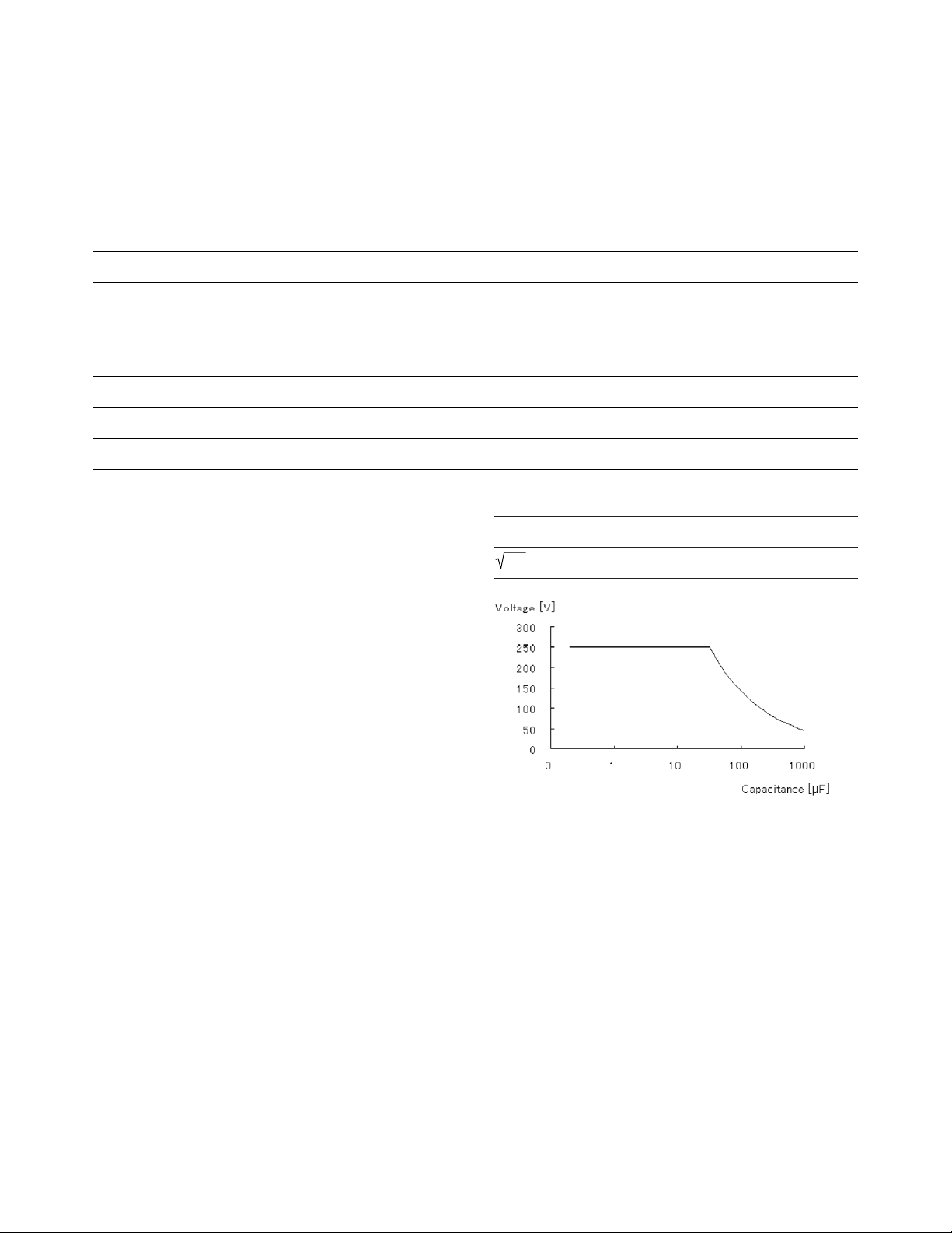
The following table shows the maximum discharge
withstand voltage below which the internal circuit
is protected even if a charged capacitor is connected to UNKNOWN terminal.
NOTE: Connect the charged capacitor to the
UNKNOWN terminals or test fixture after it has
discharged.
Maximum capacitor voltage Range of capacitance C of measured DUT
250 V C < 32 µF
2/C VC ≥ 32 µF
Table 8. Effective measurement range (D ≤ 0.5)
Effective measament range [F]
Measurement frequency: 120 Hz Measurement frequency: 1 kHz
Measurement range Minimum Maximum Minimum Maximum
1 nF — — 100 p 2 n
10 nF 1 n 20 n 1 n 20 n
100 nF 10 n 200 n 10 n 200 n
1 µF 100 n 2 µ 100 n 2 µ
10 µF1 µ 20 µ 1 µ 20 µ
100 µF 10 µ 200 µ 10 µ 200 µ
1 mF 200 µ 2 µ ——
Figure 5. Maximum capacitor voltage
Page 10

10
Sample calculation of measurement accuracy
This section gives you sample calculations of the
measurement accuracy for each measurement
parameter, assuming the measurement conditions
shown below.
Measurement frequency 1 kHz
Measurement level 1 V
Measurement range 10 µF
Measurement time Med
Ambient temperature 28 °C
Measurement parameter: Cp (or Cs)-D
The following sample calculation shows you how
to calculate the Cp (or Cs) accuracy, Cpe or
Cse [%], and the D accuracy, De, assuming that
the measured Cp (or Cs) value is 9.8765 µF and
the measured D value is 0.0123.
The measurement range is 10 µF and the measured
Cp (or Cs) value is 9.8765 µF, so therefore,
β = 10 µ/9.8765 µ = 1.0125
measurement frequency f = 1000
A = 0.14, B = 0.036 (from Table 3)
KL= 1.0/1.0 = 1 (from Table 1)
E = 0.0006
β = 10 µ/9.8765 µ =1.0125
KT= 1 (from Table 2)
Substituting these values into the equation yields
the following result:
Ae = [0.14 + 0.036 x 1 x 1.0125 + 100 x 0.0006 x
(2 x π x 1000 x 9.8765 x 10-6)] x 1 = 0.180 [%]
Because D <0.1, Cpe or Cse is ±0.180[%]. On the
other hand, the measured D value is 0.0123 and
the calculated Ae value is 0.180[%], and therefore,
using Equation 2, De = ±0.180/100 > ± 0.0018 is
obtained. As a result, the true Cp (or Cs) value
falls within 9.8765 ± (9.8765 x 0.0178 [µF], i.e., a
range between 9.8587 and 9.8943 [µF]; the true D
value, 0.0123 ± 0.0018 , falls within a range
between 0.0105 and 0.0141.
Measurement parameter: Cp (or Cs)-Q
The following sample calculation shows you how to
calculate the Cp (or Cs) accuracy, Cpe (or Cse) [%],
and the Q accuracy, Qe, assuming that the meas-
ured Cp (or Cs) value is 9.8765 µF and the measured Q value is 9.8765.
The measurement frequency is 1 kHz and the
measured Cp (or Cs) is 9.8765 µF. By performing
calculation in the same way as Cp-D, Ae = 0.180[%]
is obtained. Because D = 1/9.8765 > 0.1013 > 0.1,
multiply (1 + 0.1013
2
). The calculated Cpe or Cse is
±0.182 [%] . On the other hand, the calculated D
value is 0.1013 and the calculated Ae value is 0.180
[%]. To obtain De, first, use Equation 10-3. The
result is
De = ±(0.180/100) x (1 + 0.1013) x 1 + 0.10132> ± 0.0020
Then, use the obtained De and Equation 4. The
result is Qe = ±9.87652x 0.0020/(17 9.8765 x
0.0020) = –0.1913 ~0.1990. As a result, the true
Cp (or Cs) value falls within a range between
9.8586 and 9.8944 [µF]; the true Q value falls
within a range between 9.6852 and 10.076.
Measurement parameter: Cp-G
The following sample calculation shows you how
to calculate the Cp accuracy, Cpe [%], and the
G accuracy, Ge [%], assuming that the measured
Cp value is 9.8765 µF and the measured G value
is 0.0123.
D = 0.0123/(2 x π x 1000 x 9.8765 x 10-6) > 0.1982 >0.1
Therefore, multiply the calculated Ae value by
(1 + 0.19822). The result of Cpe is ±0.187[%].
On the other hand, from Equation 5,
Ge = ±0.180/(0.0123/(2 x π x 1000 x 9.8765 x 10-6)) =
±0.908 [%]
Because D > 0.1, multiply by (1 + 0.19822) in
the same way as Cpe. The final result of Ge is
±0.943 [%].
Page 11

11
Measurement parameter: Cp-Rp
The following sample calculation shows you how
to calculate the Cp accuracy, Cpe[%], and the Rp
accuracy, Rpe[%], assuming that the measured
Cp value is 9.8765 µF and the measured Rp value
is 123.45 Ω.
D = 1/(2 3π31000 3 9.8765 3 10
-6
3 123.45) > 0.1305 >0.1
Therefore, multiply the calculated Ae by (1 +
0.13052). The result of Cpe is ±0.183[%]. On the
other hand, Gx = 1/Rpx = 1/123.45 = 0.0081.
Therefore, perform the calculation in the same
way as Cp-G. The result of Ge is ±1.402[%]. From
Equation 6, Rpe = ±1.402/(1 7 1.042/100) = -1.383
~
1.422[%] is obtained.
Measurement parameter: Cs-Rs
The following sample calculation shows you how
to calculate the Cs accuracy, Cse [%], and the R
accuracy, Rse [%], assuming that the measured
Cs value is 9.8765 µF and the measured Rs value
is 2.3456 Ω.
D = 23πx 1000 x 9.8765 x 10-6x 2.3456 > 0.1456 >0.1
Therefore, multiply the calculated Ae by (1 +
0.14562). The result of Cse is ±0.182 [%]. On the
other hand, from Equation 7, Rse = 0.180/(2 x π x
1000 x 9.8765 x 10-6x 2.3456) > 1.237 [%]. Because
D >0.1, multiply by (1 + 0.14562) in the same way
as Cse. The final result of Rse is ±1.263 [%].
Page 12

12
Table 9 lists the Agilent 4268A GPIB commands
sorted according to function. Table 9 additionally
provides compatible Agilent 4278A1GPIB commands.
Refer to Chapter 6, GPIB Command Reference, of
the 4268A operation manual for more detail. Refer
to the 4278A operation manual for its detailed
information.
4. GPIB Command Information
Table 9. GPIB command table (4268A command vs. 4278A command)
GPIB command
Function Setting/operation Agilent 4268A Agilent 4278A
Measurement Reset :SYSTem:PRESet, *RST *RST
condition
Signal Frequency :SOURce:FREQuency[:CW] FREQ1, FREQ2
Level :SOURce:VOLTage[:Level][:MMediate][:AMPLitude] OSC =
ALC :SOURce:VOLTage:ALC[:STATe] None
Output mode :SOURce:VOLTage:MODE None
Source delay time :TRIGger[:SEQuence1]:DELay None
Parameter Primary :CALCulate1:FORMat MPAR1, MPAR2, MPAR3,
MPAR4, MPAR5, MPAR6
Secondary :CALCulate2:FORMat
Deviation On/off :CALCulate1:MATH:STATe None
measurement :CALCulate2:MATH:STATe
Mode :CALCulate1:MATH:EXPRession:NAME, None
:CALCulate2:MATH:EXPRession:NAME
Reference value :DATA[:DATA] None
Range Auto range [:SENSe][:FIMPedance]:RANGe:AUTO RAO
Range [:SENSe][:FIMPedance]:RANGe[:UPPer] RA1, RA2, RA3, RA4,
RA5, RA6, RA7
Measurement time [:SENSe][:FIMPedance]:APERture[:MODE] ITIM1, ITIM2, ITIM3
Average On/off [:SENSe]:AVERage[:STATe] None
Count [:SENSe]:AVERage:COUNt AVE=
Cable length :CALibration:CABLe CABL0, CABL1, CABL1
Trigger delay time :TRIGger:SEQuence2:DELay DTIM=
Trigger mode :TRIGger[:SEQuence1]:SOURce TRIG1, TRIG2, TRIG3
Trigger Triggering :TRIGger[:SEQuence1][:IMMediate], *TRG *TRG
Trigger system reset :ABORt None
Trigger system operation :INITiate[:IMMediate] None
Trigger system operation setting :INITiate:CONTinuous None
Data output Data transfer format setting :FORMat[:DATA] DFMT1, DFMT2
Read data :DATA[:DATA], :FETCh?, :READ? DATA?
Data transfer format :FORMat[:DATA] None
Data bufferSetting Data feed :DATA:FEED None
Feed ( yes or no)? :DATA:FEED:CONTroI None
Size:number of points :DATA:POINts None
1. Denotes the 4278A is obsolete.
Page 13

13
Table 9 continued.
GPIB command
Function Setting/operation Agilent 4268A Agilent 4278A
Comparator On/off :CALCulate:COMParator[:STATe] COMP0, COMP1
function
Primary On/off :CALCulate:COMParator:PRIMary:BIN1:STATe, None
Parameter limit :CALCulate:COMParator:PRIMary:BIN{2-9}:STATe
Limit setting :CALCulate:COMParator:PRIMary:BIN1, BIN 1=, BIN2=, BIN3=,
:CALCulate:COMParator:PRIMary:BIN{2-9} BIN4=, BIN5=, BIN6=,
BIN7=, BIN8=, BIN9=,
BLIM=
Mode setting :CALCulate:COMParator:MODE None
Reference value :CALCulate:COMParator:PRIMary:NOMinal NOM=
Secondary parameter limit On/off :CALCulate:COMParator:SECondary:STATe None
Area :CALCulate:COMParator:SECondary:LIMit SLIM=
AUX BIN function On/off :CALCulate:COMParator:AUXBin AUX0, AUX1
BIN count function On/off :CALCulate:COMParator:COUNt[:STATe] CNT0, CNT1
Clear count :CALCulate:COMParator:COUNt:CLEar RCNT
Count data :CALCulate:COMParator:COUNt:DATA? COUN?
Correction User correction function on/off [:SENSe]:CORRection[:STATe] OPEN0, OPEN1, SNOR0,
function SNOR1, STD0, STD1
Load correction function on/off [:SENSe]:CORRection:COLLect:METNod STD0, STD1
Measure correction data [:SENSe]:CORRection:COLLect[:ACQuire] XOP, XSH, XST
Set correction data [:SENSe]:CORRection:DATA None
Read data correction [:SENSe]:CORRection:DATA OPM?, STM?, STM
Standard value for load Standard value [:SENSe]:CORRection:CKIT:[STANdard3] CSTD=, DSTD=, GSTD=,
correction STR?
Parameter type [:SENSe]:CORRection:CKIT:STANdard3:FORMat SPAR1, SPAR2
Scanner Multi channel correction On/off [:SENSe]:CORRection:MULTiple:[STATe] MCOM0, MCOM1
function
Channel number setting [:SENSe]:CORRection:MULTipIe:CHANneI CNO=
Load standard value [:SENSe]:CORRection:MULTipIe:CKIT:STANdard3 None
(ALL or each channel) [:STATe]
Other Current monitor On/off :CALCulate3:MATH:STATe None
measurement
Read display data :DATA[:DATA] None
support
Voltage monitor On/off :CALCulate4:MATH:STATe None
functions
Read display data :DATA[:DATA] None
Contact check function on/off [:SENSe][:FIMPedance]:CONTact:VERify None
Save/recall Save *SAV STO
Recall *RCL LOAD
Display On/off :DISPIay[:WINDow][:STATe] None
Display setting :DISPIay[:WINDow]:TEXT1 [:DATA]:DIGit DDIG4, DDIG5, DDIG6
Display page setting :DISPIay[:WINDow]:TEXT2:PAGE VMON0, VMON1, VMON2,
VMON3, VMON4, VMON5,
VMON6
Key lock function on/off :SYSTem:KLOCk None
Beep output On/off :CALCulate:COMParator:BEEPer[:STATe]:SYSTem: None
BEEPer:STATe
Mode :CALCulate:COMParator:BEEPer:CONDition None
Beep sound output :SYSTem:BEEPer[:IMMediate] None
Page 14

14
Table 9 continued.
GPIB command
Function Setting/operation Agilent 4268A Agilent 4278A
Status Clear *CLS *CLS
reporting
Read satus byte register value *STB? *STB?
structure
Mask setting for service request *SRE *SRE
Enable register
Standard event Read register value *ESR? None
Status register OPC bit setting when *OPC None
operation completes
Mask setting for enable *ESE None
register
Standard Clear :STATus:PRESet None
Operation Read register value :STATus:OPERation:CONDition?, None
Status group :STATus:QUEStionabIe:CONDition
Mask setting for enable :STATus:OPERation:ENABIe, None
register :STATus:QUEStionabIe:ENABIe
Read event register :STATus:OPERation[:EVENt]?, None
value :STATus:QUEStionable[:EVENt]
Others Self test operation *TST? TENT, TNO=, TST, TAB,
TDA?, TEND
Read product information *IDN? *IDN?
Read option information *OPT? *OPT?
Read 1 when operation completes *OPC? None
Read error Information :SYSTem:ERRor? ERR?
Read SCPI version :SYSTem:VERSion? None
Wait for command *WAI None
Page 15
15
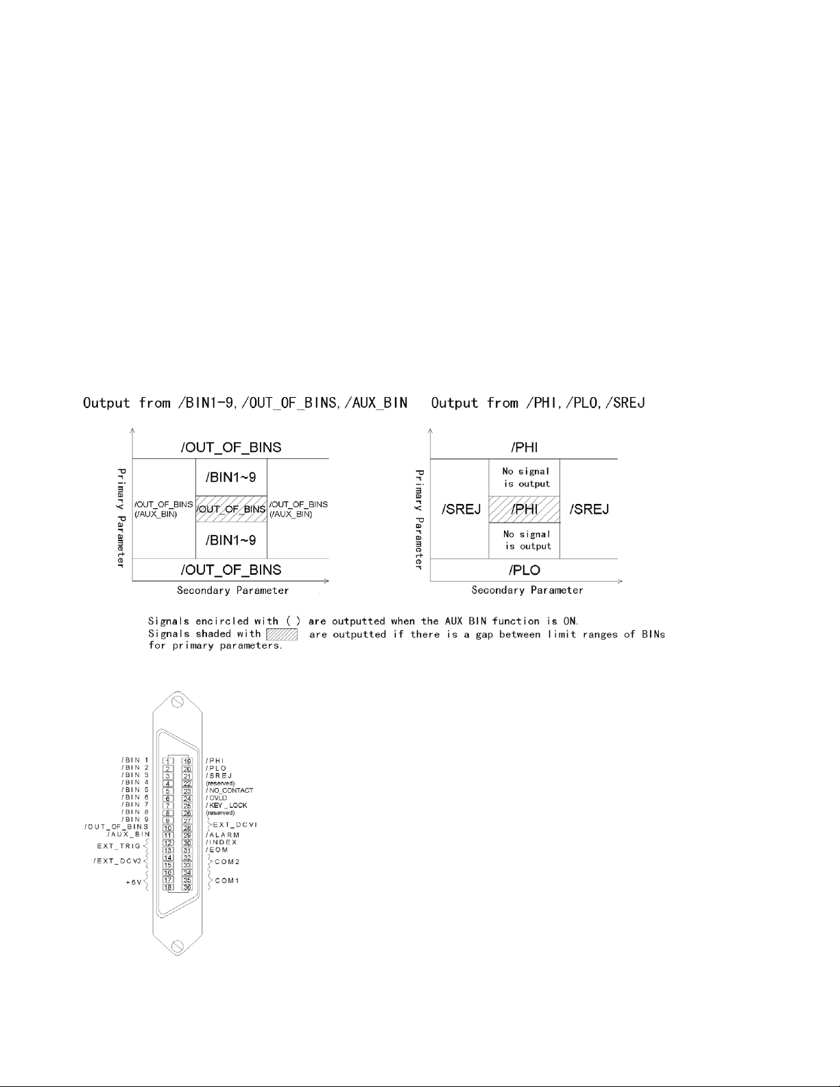
Outputting the comparator result
Via the handler interface, the sorting result of the
comparator is outputted. The relationship between
the comparator result and the output signals of the
handler interface (/BIN1- /BIN9, /AUX BIN, /OUT
OF BINS, /PHI, /PLO, /SREJ) is shown below.
NOTE: If the comparator function is OFF, the signals
are not outputted except for /INDEX, /EOM, and
/ALARM. /INDEX and /EOM are kept outputted
(Low). /ALARM is outputted when an error occurs,
in the same way as when the comparator is ON.
Note that EXT TRIG is valid, regardless of ON/OFF
of the comparator function, if the trigger mode is
Ext (external).
Pin assignment of the Input/output signals
Figure 7 shows the pin assignment of each
input/output signal of the handler interface
connector. Table 10 describes the input/output
signals.
NOTE: The / (slash) before signal names means that
the signal is negative logic (active low).
5. Handler Interface Information
Figure 6. Output of the comparator result to the handler interface
Figure 7. Pin assignment of the handler interface connector
Page 16

16
Table 10. Description of the handler interface input/output signals
Pin number Signal name Description
1 /BIN1 Screening result signals (output). A BIN signal for the screening result (one of pins 1 to 11) goes Low. Note that, if a contact
2 /BIN2
check failure occurs or if measurement is impossible, these signals do not go Low.
3 /BIN3
4 /BIN4
5 /BIN5
6 /BIN6
7 /BIN7
8 /BIN8
9 /BIN9
10 /OUT_OF_BINS
11 /AUX_BIN
12,13 EXT_TRIG External trigger signals (input). These are valid when the trigger mode is set to EXt (external). The rising edge of a pulse
generates a trigger.
14,15 EXT_DCV2 External DC voltage (input). These supply voltage for the input signals (EXT TRIG, /KEY LOCK) and the operation output sig-
nals (/ALARM, /INDEX, /EOM). The input voltage range is from + 5 V to + 15 V.
16,17,18 + 5V Internal DC voltage (output).
19 /PHI Over primary parameter upper limit signal (output). If the upper limit value of BIN1 to BIN9 is exceeded, it goes Low.
20 /PLO Below primary parameter lower limit signal (output). If the lower limit value of BIN1 to BIN9 is not reached, it goes Low.
21 /SREJ Secondary parameter out-of-limit signal (output). If the secondary parameter goes out of the allowable limit, it goes Low.
22 (reserved) Not used at present. Do not connect anything.
23 /NO_CONTACT Contact check failure signal (output). If the contact check is failed, it goes Low.
24 /OVLD Measurement impossibility signal (output). If the measurement is impossible at the analog measurement part, it goes Low.
25 /KEY_LOCK Key lock signal (input). Setting this signal to Low disables the use of all the front panel keys of the Agilent 4268A.
26 (reserved) Not used at present. Do not connect anything.
27, 28 EXT DCV1 External DC voltage (input). These supply voltage for the judgement output signals (/BIN1-/BIN9, /AUX BIN, /OUT OF
BINS, /PHI, /PLO, /SREJ, /OVLD, /NO CONTACT). The input voltage range is from +5 V to +24 V.
29 /ALARM Error occurrence signal (output). In the case of abnormal selftest result, momentary failure of the power supply, or abnormal
operation of a certain circuit, it goes Low. In the case of momentary failure of the power supply, it is Low only while the
power supply is down.
30 /INDEX Analog measurement completion signal (output). When the analog measurement is completed, it goes Low. When the han-
dler receives this signal, it gets ready for the next DUT to be connected. Note that, until it receives the /EOM signal, measurement data cannot be obtained.
31 /EOM Measurement cycle completion signal (output). When a series of measurement steps is completed and the measurement
data screening result becomes valid, it goes Low.
32, 33 COM2 Common for the external DC voltage of EXT DCV2 (pins 14 and 15).
34, 35, 36 COM1 Common for the external DC voltage of EXT DCV1(pins 27 and 28).
Page 17

17
Timing chart
Figure 8 shows the timing chart. T1 through T5 indicate the time periods described in the following
table. The undefined section in /Data indicates that
the 4268A is processing data after analog measurement and therefore the output signal is invalid.
Time Minimum Maximum
T1 Trigger pulse width 1[µs] —
T2 Measurement start delay time — 600[µs]
1
T3 Screening result output hold time 0[µs] —
T4 Screening result output setup time 1[µs] —
T5 Trigger setup time 0[µs] —
Electrical characteristics
Output signals
Each output signal is outputted via open collector
using photo-coupler. Voltage of each output is
obtained by connecting pull-up resistors, inside
or outside of the 4268A. The output signals can
be divided into two groups: judgment output signals and operation output signals. Table 11 shows
the electrical characteristics of the output signals.
Figure 9 and Figure 10 show the circuit diagram of
the judgment output signals and that of the operation output signals, respectively.
Table 11. Electrical characteristics of the handler interface output signals
Output signal Output voltage [V] Maximum
Low High current [mA]
Judgment output signals 0 to 0.5 DCV12 6
/BIN1 to /BIN9, /AUX_BIN,
/OUT_OF_BINS, /PHI /PLO,
/SREJ, /OVLD, /NO_CONTACT
Operation output signals 0 to 0.5 DCV236
/INDEX, /EOM, /ALARM
Figure 8. Timing chart
1. When the display has been turned off.
2. +5 V or +12 V when internal power supply used.
EXT_DCV2(+5 V to +15 V) when external power supply used.
3. +5 V or +12 V when internal power supply used.
EXT_DCV2(+5 V to +15 V) when external power supply used.
Page 18

18
Figure 9. Circuit diagram of the handler interface input signals
Handler I/F
connector
A1 main board
Figure 10. Circuit diagram of the handler interface operation output signals
Handler I/F
connector
A1 main board
Page 19

19
Figure 11. Circuit diagram of the handler interface input signals
Input signals
Each input signal is connected to the LED (cathode
side) of the photo-coupler. The LED (anode side)
is connected to the pull-up power supply voltage.
Table 12 shows the electrical characteristics of the
input signals. Figure 11 shows the circuit diagram
of the input signals. The amount of the current
flowing through the LED varies, depending on the
pull-up power supply voltage and the setting of the
pull-up resistor setting switch (S2). For information
on the pull-up power supply voltage and the setting
of S2, refer to Preparation for Using the Handler
Interface on page 20.
Table 12. Electrical characteristics of the handler interface input signals
Input current (at Low) [mA] (typical)
Input signal Input voltage [V] Pull-up power supply voltage DCV2
1
Low High 5V 12V 15V
EXT_TRIG 0 to 1 DCV213.7 4.6 5.9
/KEY_LOCK 0 to 1 DCV2151418
Power supply
The power supply for the judgment output signal
pull-up and that for the operation output signal
pull-up and input signal drive can be set separately.
As shown below, you can select them from +5 V or
+12 V of the internal power supply or external power
supply. For information on how to select the power
supply, refer to Setting the jumper (P17) on page 20.
Table 13. Selecting the input/output signal pull-up/drive power supply
Internal power supply External power supply
Judgment output signal
pull-up power supply + 5 V + 12 V EXT_DCV1 +5 V to +24 V
Operation output signal
pull-up power supply
and input signal drive
power supply + 5 V + 12 V EXT_DCV2 +5 V to +15 V
Table 14. Setting of circuit common
When internal When external
power supply used power supply used
Judgment output signal
pull-up power supply Internal common COM1
Operation output signal
pull-up power supply Internal common COM2
1. +5V or +12V when internal power supply used EXT_DCV2 (+5V to +15V) when
external power supply used
Page 20

Preparation for using the handler interface
Before using the handler interface, you are
required to set the input/output signal drive/
pull-up power supplies and the pull-up resistors.
NOTE: The information described here is designed
for Internal Use Only in the Agilent service center.
Request the service center to perform the setting
described here as necessary to use the handler
interface.
Setting the drive/pull-up power supply
The drive/pull-up power supply is set using the
jumper (P17) and the DIP switch (S2) on the A1
main board. For information on the location and
socket numbers of P17, and the location and switch
numbers of S2, refer to Figure 12.
Setting the jumper (P17)
P17-6, P17-7, and P17-8 let you set the operation
output signal pull-up and input signal drive power
supply (DCV2). Setting one of the following
jumpers selects external power supply (EXT
DCV2), internal power supply (+12 V), or internal
power supply (+5 V).
Socket Power supply setting when the jumper Factory
number is set (shorted) setting
P17-8 For the operation output signal pull-up and input Short
signal drive power supply, external power supply
(EXT DCV1) is specified.
P17-7 For the operation output signal pull-up and input Open
signal drive power supply, internal power supply
(+ 12 V) is specified.
P17-6 For the operation output signal pull-up and input Open
signal drive power supply, internal power supply
(+ 5 V) is specified.
NOTE: Set (short) only one of P17-6, P17-7, and P17-8.
Do not set (short) two or more at the same time.
NOTE: P17-5 and P17-4 are not used at present. Do
not connect anything.
P17-3, P17-2, and P17-1 let you set the judgment
output signal pull-up power supply (DCV1). Setting
one of the following jumpers selects external power
supply (EXT DCV1), internal power supply (+12 V),
or internal power supply (+5 V).
20
Figure 12. A1 main board
Page 21

21
Socket Power supply setting when the jumper Factory
number is set (shorted) setting
P17-3 For the judgment output signal pull-up power supply, Short
external power supply (EXT DCV1) is specified
P17-2 For the judgment output signal pull-up power supply, Open
internal power supply (+ 12 V) is specified.
P17-1 For the judgment output signal pull-up power supply, Open
internal power supply (+5 V) is specified.
NOTE: Set (short) only one of P17-3, P17-2, and P17-1.
Do not set (short) two or more at the same time. The
external power supplies (EXT DCV1 and EXT DCV2)
must be set within the following voltage ranges.
Voltage range [V)
EXT_DCV1 +5 to +24
EXT_DCV2 +5 to +15
Setting the jumpers (P18, P19)
P17-5 and P17-4 let you set the circuit common.
Socket Circuit common setting when the jumper Factory
number is set (shorted) setting
P18 External power supply’s (EXT DCV2) common Short
1-2 (COM2) and 4268A’s internal circuit common are
not connected. The operation output signals and
input signals are isolated.
P18 External power supply’s (EXT DCV2) common Open
2-3 (COM2) and 4268A’s internal circuit common are
connected. The operation output signals and input
signals are not isolated.
P19 External power supply’s (EXT DCV1) common Short
1-2 (COM1) and 4268A’s internal circuit common are not
connected. The judgment output signals are isolated.
P19 External power supply’s (EXT DCV1) common Open
2-3 (COM1) and 4268A’s internal circuit common are
connected. The judgment output signals are not
isolated.
NOTE: When using +5 V (pins 16, 17, and 18) of the
handler interface connector, set (short) 2-3 of P18
or 2-3 of P19 to connect 4268A’s internal circuit
common and COM1 or COM2 so that COM1 or
C0M2 is used as the power supply circuit common.
Setting the switch ( S2 )
Each switch of the switch (S2) must be set as follows, depending on the voltage setting of the operation output signal pull-up and input signal drive
power supply (DCV2).
Voltage setting of the operation output signal pull-up and
input signal drive power supply (DCV2)
5 V ≤DCV2 ≤6 6 V <DCV2 ≤9 V 9 V <DCV2 ≤15
(factory setting)
Page 22

Setting the pull-up resistors
The pull-up resistors for the operation output signals and judgment output signals must be set using
J12 and J13 on the A1 main board. The following
table shows the location where the resistor for
each signal should be mounted, the equation to
calculate the pull-up resistor values, and the typical
resistance values. For information on the location
of J12 and J13 and the location of the resistors for
J12 and J13, refer to Figure 12.
22
Typical resistance value [kΩ]
DCV1 or DCV2 voltage
Signal Name Resistor location Resistance value [kΩ] 5 V 9 V 12 V 15 V 24 V
/OUT_OF_BINS R1-1 DCV1/3 1.78 3.16 4.22 5.11 8.25
/BIN1 R1-2 DCV1/3 1.78 3.16 4.22 5.11 8.25
/BIN2 R1-3 DCV1/3 1.78 3.16 4.22 5.11 8.25
: : : :::::
/BIN8 R1-9 DCV1/3 1.78 3.16 4.22 5.11 8.25
/BIN9 R1-10 DCV1/3 1.78 3.16 4.22 5.11 8.25
/AUX_BIN R1-11 DCV1/3 1.78 3.16 4.22 5.11 8.25
/PHI R2-1 DCV1/3 1.78 3.16 4.22 5.11 8.25
/PLO R2-2 DCV1/3 1.78 3.16 4.22 5.11 8.25
/SREJ R2-3 DCV1/3 1.78 3.16 4.22 5.11 8.25
(reserved) R2-4 — —————
/NO_CONTACT R2-5 DCV1/3 1.78 3.16 4.22 5.11 8.25
/OVLD R2-6 DCV1/3 1.78 3.16 4.22 5.11 8.25
(reserved) R2-7 — —————
(reserved) R2-8 — —————
/ALARM R2-9 DCV2/3 1.78 3.16 4.22 5.11 —
/INDEX R2-10 DCV2/3 1.78 3.16 4.22 5.11 —
/EOM R2-11 DCV2/3 1.78 3.16 4.22 5.11 —
The product numbers of the resistors are as follows:
1.78 kΩ 0757-0278
3.16 kΩ 0757-0279
4.22 kΩ 0698-3154
5.11 kΩ 0757-0438
8.25 kΩ 0757-0441
The resistors are not factory-mounted. R2-4, R2-7,
and R2-8 are reserved. Do not connect anything.
Page 23

Procedure to remove the cover
This section describes how to disconnect the cables
that hinder the operator from removing and
attaching the cover when setting the drive/pull-up
power supply or mounting pull-up resistors.
WARNING: Perform this work when 10 minutes or more
have elapsed after disconnecting the power cord. When
the 4268A is operating, or immediately after the power is
turned off, dangerous electrical energy or voltage exists.
Therefore, sufficient time is required after disconnecting
the power cord to discharge the internal capacitor.
NOTE: When removing the cover, setting the
drive/pull-up power supply, and mounting pull-up
resistors, perform the work in a place with static
protection, wearing a ground strap.
Step 1. Disconnect Agilent 4268A’s power cord and
wait for 10 minutes.
Step 2. Remove the two screws that secure the
cover on the rear panel of the chassis.
Step 3. While holding the front panel bezel, slide
the cover backward to remove it.
Step 4. Disconnect the cable connected to the A2
CPU board from the GPIB connector on the rear
panel.
Step 5. If the scanner interface (option) is installed,
disconnect the cable connected to the A1 mainboard from the scanner interface connector on the
rear panel.
NOTE: When mounting pull-up resistors, exercise
care not to damage surrounding parts (including
cables and connectors) with a soldering iron or
otherswise.
23
Page 24

Agilent Technologies’ Test and Measurement Support, Services, and Assistance
Agilent Technologies aims to maximize the value you receive, while minimizing
your risk and problems. We strive to ensure that you get the test and measurement
capabilities you paid for and obtain the support you need. Our extensive support
resources and services can help you choose the right Agilent products for your
applications and apply them successfully. Every instrument and system we sell has
a global warranty. Support is available for at least five years beyond the production
life of the product. Two concepts underlie Agilent’s overall support policy: “Our
Promise” and “Your Advantage.”
Our Promise
Our Promise means your Agilent test and measurement equipment will meet its
advertised performance and functionality. When you are choosing new equipment, we
will help you with product information, including realistic performance specifications
and practical recommendations from experienced test engineers. When you use
Agilent equipment, we can verify that it works properly, help with product operation,
and provide basic measurement assistance for the use of specified capabilities, at
no extra cost upon request. Many self-help tools are available.
Your Advantage
Your Advantage means that Agilent offers a wide range of additional expert test and
measurement services, which you can purchase according to your unique technical
and business needs. Solve problems efficiently and gain a competitive edge by
contracting with us for calibration, extra-cost upgrades, out-of-warranty repairs,
and onsite education and training, as well as design, system integration, project
management, and other professional engineering services. Experienced Agilent
engineers and technicians worldwide can help you maximize your productivity,
optimize the return on investment of your Agilent instruments and systems, and
obtain dependable measurement accuracy for the life of those products.
Agilent T&M Software and Connectivity
Agilent’s Test and Measurement software and connectivity products, solutions and
developer network allows you to take time out of connecting your instruments to
your computer with tools based on PC standards, so you can focus on your tasks,
not on your connections. Visit
www
.agilent.com/find/connectivity
for more information.
By internet, phone, or fax, get assistance with all your
test & measurement needs
Online Assistance:
www.agilent.com/find/assist
Product specifications and descriptions in this document
subject to change without notice.
© 2003 Agilent Technologies, Inc.
Printed in USA, April 28, 2003
5968-3970E
Phone or Fax
United States:
(tel) 800 452 4844
Canada:
(tel) 877 894 4414
(fax) 905 282 6495
China:
(tel) 800 810 0189
(fax) 800 820 2816
Europe:
(tel) (31 20) 547 2323
(fax) (31 20) 547 2390
Japan:
(tel) (81) 426 56 7832
(fax) (81) 426 56 7840
Korea:
(tel) (82 2) 2004 5004
(fax) (82 2) 2004 5115
Latin America:
(tel) (305) 269 7500
(fax) (305) 269 7599
Taiwan:
(tel) 0800 047 866
(fax) 0800 286 331
Other Asia Pacific Countries:
(tel) (65) 6375 8100
(fax) (65) 6836 0252
Email:
tm_asia@agilent.com
www.agilent.com/find/emailupdates
Get the latest information on the products
and applications you select.
 Loading...