

Page 1

PCI-8154
Advanced & Modulized
4-Axis Servo / Stepper
Motion Control Card
User’s Manual
Manual Rev. 2.00
Revision Date: February 22, 2006
Part No: 50-11146-1000
Advance Technologies; Automate the World.
Page 2

Copyright 2007 ADLINK TECHNOLOGY INC.
All Rights Reserved.
The information in this document is subject to change without prior
notice in order to improve reliability , design, and function and does
not represent a commitment on the part of the manufacturer.
In no event will the manufacturer be liable for direct, indirect, special, incidental, or consequential damages arising out of the use or
inability to use the product or documentation, even if advised of
the possibility of such damages.
This document contains proprietary information protected by copyright. All rights are reserved. No part of this manual may be reproduced by any mechanical, elec tronic, or other means in a ny form
without prior written permission of the manufacturer.
Trademarks
NuDAQ, NuIPC, DAQBench are registered trademarks of ADLINK
TECHNOLOGY INC.
Product names mentioned herein are used for identification pur-
poses only and may be trademarks and/or registered trademarks
of their respective companies.
Page 3

Getting Service from ADLINK
Customer Satisfaction is top priority for ADLINK Technology Inc.
Please contact us should you require any service or assistance.
ADLINK TECHNOLOGY INC.
Web Site: http://www.adlinktech.com
Sales & Service: Service@adlinktech.com
TEL: +886-2-82265877
FAX: +886-2-82265717
Address: 9F, No. 166, Jian Yi Road, Chungho City,
Taipei, 235 Taiwan
Please email or FAX this completed service form for prompt and
satisfactory service.
Company Information
Company/Organization
Contact Person
E-mail Address
Address
Country
TEL FAX:
Web Site
Product Information
Product Model
OS:
Environment
M/B: CPU:
Chipset: BIOS:
Please give a detailed description of the problem(s):
Page 4

Page 5

Table of Contents
Table of Contents..................................................................... i
List of Tables........................................................................... v
List of Figures........................................................................ vi
1 Introduction ........................................................................ 1
1.1 Features............................................................................... 4
1.2 Specifications....................................................................... 6
1.3 Supported Software............................................................. 8
Programming Library ........................................ ... ...........8
MotionCreatorPro ........................................................... 8
1.4 Available Terminal Board..................................................... 8
2 Installation .......................................................................... 9
2.1 Package Contents ............................................................... 9
2.2 PCI-8154 Outline Drawing................................................. 10
2.3 PCI-8154 Hardware Installation......................................... 11
Hardware configuration .................................................11
PCI slot selection ................. ... ... .... ... ... ... ......................11
Installation Procedures .................................................11
Troubleshooting4: ................................ ......................... 11
2.4 Software Driver Installation................................................ 13
2.5 CN3 Pin Assignments: Main Connector ............................ 13
2.6 K1/K2 Pin Assignments: Simultaneous Start/Stop ............ 15
2.7 JP2 to JP9 Jumper Setting for Pulse Output ..................... 15
2.8 SW1 Card Index Selection................................................. 16
2.9 CN4 Manual Pulsar............................................................ 17
3 Signal Connections.......................................................... 19
3.1 Pulse Output Signals OUT and DIR .................................. 20
3.2 Encoder Feedback Signals EA, EB and EZ....................... 23
3.3 Origin Signal ORG............................................................. 26
3.4 End-Limit Signals PEL and MEL........................................ 27
3.5 In-position Signal INP ........................................................ 28
3.6 Alarm Signal ALM.............................................................. 29
3.7 Deviation Counter Clear Signal ERC................................. 30
3.8 General-purpose Signal SVON............... ... ... ... .... ... ... ... .... . 31
Table of Contents i
Page 6

3.9 General-purpose Signal RDY ............................................ 32
3.10 Multi-Functional output pin: DO/CMP ................................ 33
3.11 Multi-Functional input pin: DI/LTC/SD/PCS/CLR/EMG...... 34
3.12 Pulser Input Signals PA and PB (PCI-8154)...................... 35
3.13 Simultaneously Start/Stop Signals STA and STP.............. 36
4 Operation Theory.............................................................. 39
4.1 Classifications of Motion Controller.................................... 39
Voltage motion control interface ................................... 39
Pulse motion control interface ......................................40
Network motion control interface .................................. 40
Software real-time motion control kernel ..................... .41
DSP motion control kernel ............................................41
ASIC motion control kernel ...........................................41
Compare Table of all motion control types ...................42
PCI-8154 motion controller type ...................................42
4.2 Motion Control Modes........................................................ 43
Coordinate system ........................................................43
Absolute and relative position move .............................44
Trapezoidal speed profile .............................................45
S-curve and Bell-curve speed profile .................. .......... 46
Velocity mode ...............................................................48
One axis position mode ................................................49
Two axes linear interpolation position mode .................50
Two axes circular interpolation mode ...........................51
Continuous motion ........................................................52
Home Return Mode ......................................................55
Home Search Function .................................................62
Manual Pulser Function ................................................63
Simultaneous Start Function .........................................63
Speed Override Function ..............................................64
Position Override Function ...........................................65
4.3 The motor driver interface.................................................. 66
Pulse Command Output Interface ................................66
Pulse feedback input interface ......................................69
In position signal ... .... ... ... ... .... ... ... ... ..............................71
Servo alarm signal ........................................................71
Error clear signal ...........................................................72
Servo ON/OFF switch ..................... ..............................72
Servo Ready Signal ......................................................73
ii Table of Contents
Page 7

Servo alarm reset switch ..............................................73
4.4 Mechanical switch interface............................................... 74
Original or home signal .................................................74
End-Limit switch signal .................................................74
Slow down switch .........................................................74
Positioning Start switch .................................. ... ... ... .... .. 75
Counter Clear switch ....................................................75
Counter Latch switch ....................................................75
Emergency stop input ...................................................75
4.5 The Counters................................................... .... ... ... ... .... . 76
Command position counter ...........................................76
Feedback position counter .......................................... .. 77
Command and Feedback error counter ........................77
General purpose counter .............................................. 78
Target position recorder ............................. .... ... ... ... .... .. 78
4.6 The Comparators............................. .................................. 79
Soft end-limit comparators ............................................79
Command and feedback error counter comparators ....79
General comparator ......................................................79
Trigger comparator .......................................................80
4.7 Other Motion Functions ..................................................... 81
Backlash compensation and slip corrections ................81
Vibration restriction function .........................................81
Speed profile calculation function .................................82
4.8 Interrupt Control................................................................. 83
4.9 Multiple Card Operation..................................................... 87
5 MotionCreatorPro............................................................. 89
5.1 Execute MotionCreatorPro ..................... ... ... ..................... 89
5.2 About MotionCreatorPro.................................................... 90
5.3 MotionCreatorPro Introduction........................................... 91
Main Menu ....................................................................91
Select Menu .................................................................. 92
Card Information Menu .................................. ............... 93
Configuration Menu .......... ... ... ... .... ... ... ... ... .... ... ... ... .... .. 94
Single Axis Operation Menu .......................................100
Two-Axis and Four-Axis Operation Menu ................... 108
2D_Motion Menu ........................................................112
Help Menu ..................................................................119
Table of Contents iii
Page 8

6 Function Library.............................................................. 121
6.1 List of Functions. ... ... ... .......................................... .... ... ... . 122
6.2 C/C++ Programming Library............................................ 131
6.3 System and Initialization.................................................. 132
6.4 Pulse Input/Output Configuration..................................... 136
6.5 Velocity mode motion................................ ... ... ... ... .... ... ... . 139
6.6 Single Axis Position Mode ............................................... 142
6.7 Linear Interpolated Motion............................................... 146
6.8 Circular Interpolation Motion.... .... ... ... ... .... ... .................... 155
6.9 Helical Interpolation Motion.......................... .................... 162
6.10 Home Return Mode...................................... ... ... ... .... ... ... . 166
6.11 Manual Pulser Motion............................... ... ... ... ... .... ... ... . 169
6.12 Motion Status................................................................... 172
6.13 Motion Interface I/O ......................................................... 174
6.14 Interrupt Control................................................. .............. 182
6.15 Position Control and Counters......................................... 186
6.16 Position Compare and Latch............................................ 191
6.17 Continuous motion........................................................... 196
6.18 Multiple Axes Simultaneous Operation............................ 198
6.19 General-Purpose DIO.................................. ... ... ... .... ... ... . 201
6.20 Soft Limit............ ... ... ... .... ... ... ... .... .................................... 203
6.21 Backlash Compensation / Vibration Suppression........... . 205
6.22 Speed Profile Calculation................................................. 207
6.23 Return Code.................................... ... .............................. 211
7 Connection Example ...................................................... 213
7.1 General Description of Wiring.. .... ... ... ... .... ... .................... 213
7.2 Terminal Board User Guide............................................. 213
Warranty Policy ................................................................... 215
iv Table of Contents
Page 9

List of Tables
Table 2-1: CN3 Pin Assignments: Main Connector ................. 13
Table 2-2: K1/K2 Pin Assignments: Simultaneous Start/Stop . 15
Table 2-3: SW1 Card Index ..................................................... 16
Table 2-4: CN4 Manual Pulsar ................................................ 17
Table 4-1: Motion Interrupt Source Bit Settings ....................... 84
Table 4-2: Error Interrupt return codes .................................... 85
Table 6-1: Data type definitions ............................................. 131
List of Tables v
Page 10

List of Figures
Figure 1-1: PCI-8154 Block Diagram ........................................... 2
Figure 1-2: Flow chart for building an application ........................ 3
Figure 2-1: PCB Layout of the PCI-8154 ................................... 10
vi List of Figures
Page 11

1 Introduction
The PCI-8154 is an advanced & modulized 4-axis motion controller card with a PCI interface. It can generate high frequ ency pulses
(6.55MHz) to drive stepper or servomotors. As a motion controller,
it can provide 4-axis linear and circular interpolation and continu ous interpolation for continuous velocity. Also, changing position/
speed on the fly is available with a single axis operation.
Multiple PCI-8154 cards can be used in one system. Incremental
encoder interfaces on all eight axes provide the ability to correct
positioning errors generated by inaccurate mechanical transmissions.
The PCI-8154 is a completely new design. This carrier board has
4-axis pulse train output control channels. For additional functions,
such as high-speed triggering or distributed I/O control, you can
add on a daughter board based on requirement. This board has
position compare function. Like the line scan application, the application needs motion controller to generate high speed triggering
pulse and gain the high resolution images. In this situation, you
can adopt a DB-8150 to extend the function on PCI-8154. In addition to motion control, sensors and actuators are key elements in
machine automation. There typically needs to I/O to integrate the
sensors and actuators in the contro ller. ADLINK also provides you
another way to connect these devices: distributed I/O. Using
daughter board, distributed I/O can be achieved with PCI-8154.
This cost-effective configuration can reduce wiring ef fort and physical controller size.
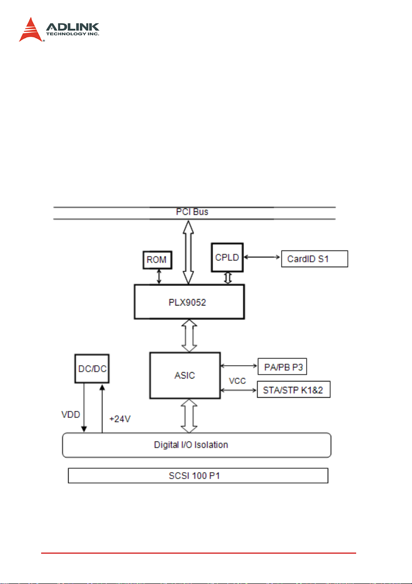
Figure 1-1 shows the functional block diagram of the PCI-8154
card. The motion control functions include trapezoidal an d S-curve
acceleration/deceleration, linear and circular interpolation between
two axes and continuous motion positioning, and 13 home return
modes. All these functions and complex computations are performed internally by the ASIC, thus it can save CPU loading.
The PCI-8154 also offers three user-friendly functions.
1. Card Index Setting:
Introduction 1
Page 12
The card index value of the PCI-8154 can be set with a DIP
switch to a value between 0 and 15. This is useful for machine
makers if the whole control system is very huge.
2. Emergency Input
An emergency input pin can be wired to an emergency button
to stop sending pulse output once activated.
3. Software’s Security Protection
To secure applications, a 16-bit value can be set in the
EEPROM to prevent copying of custom programs.
Figure 1-1: PCI-8154 Block Diagram
2Introduction
Page 13
MotionCreatorPro is a Windows-based application development
software package included with the PCI-8154. MotionCreatorPro
is useful for debugging a motion control system during the design
phase of a project. An on-screen display lists all installed axes
information and I/O signal status of the PCI-8154.
Windows programming libraries are also provided for C++ compilers and Visual Basic. Sample programs are provided to illustrate
the operations of the functions.
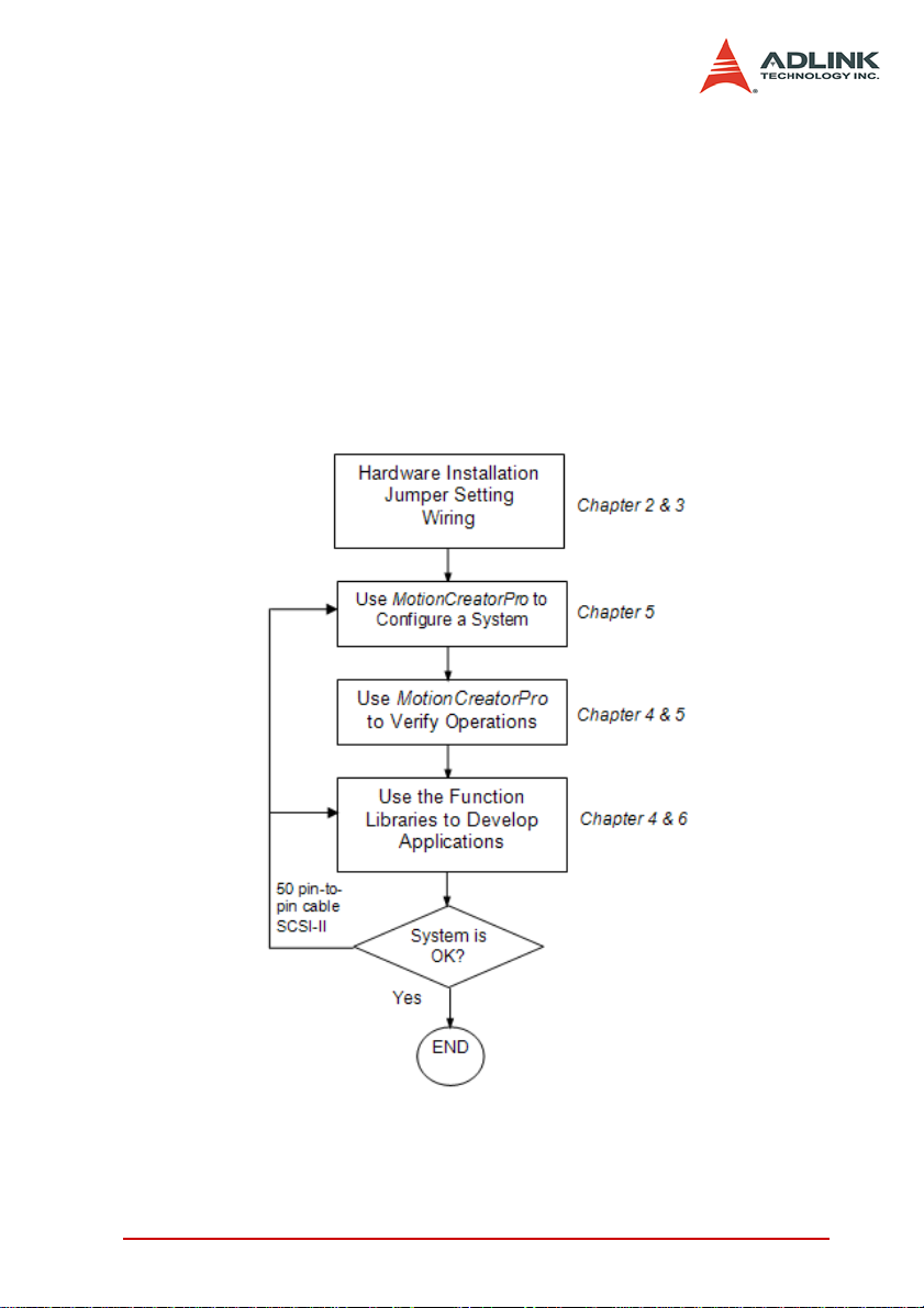
Figure 1-2 illustrates a flow chart of the recommended process in
using this manual in developing an application. Refer to the
related chapters for details of each step.
Figure 1-2: Flow chart for building an application
Introduction 3
Page 14

1.1 Features
The following list summarizes the main features of the PCI- 8154
motion control system.
X 32-bit PCI bus Plug-and-Play (Universal)
X 4 axes of step and direction pulse output for controlling
stepping or servomotor
X Maximum output frequency of 6.55MPPS
X Pulse output options: OUT/DIR, CW/CCW, AB phase
X Pulse input options: CW/CCW, AB phase x1, x2, x4
X Maximum pulse input frequency of 3.2Mhz in CW/CCW or
AB phase X1 mode (AB phase x4 can reach 6.5Mhz).
X Programmable acceleration and deceleration time for all
modes
X Trapezoidal and S-curve velocity profiles for all modes
X 2 to 4 axes linear interpolation
X 2 axes circular interpolation
X Continuous interpolation for contour following motion
X Change position and speed on the fly
X 13 home return modes with auto searching
X Hardware backlash compensator and vibration suppression
X 2 software end-limits for each axis
X 28-bit up/down counter for incremental encoder feedback
X Home switch, index signal (EZ), positive, and negative end
limit switches interface on all axes
X 4-axis high speed position latch input
X 4-axis position compare and trigger output
X All digital input and output signals are 2500V
X Programmable interrupt sources
X Simultaneous start/stop motion on multiple axes
X Manual pulser input interface
X Card index selection
X Security protection on EERPOM
isolated
rms
4Introduction
Page 15

X Dedicated emergency input pin for wiring
X Software supports a maximum of up to 12 PCI-8154 cards
operation in one system
X Compact PCB design
X Includes MotionCreatorPro, a Microsoft Windows-based
application development software
X PCI-8154 libraries and utilities for Windows 2000/XP/Vista.
Introduction 5
Page 16

1.2 Specifications
Applicable Motors:
X Stepping motors
X AC or DC servomotors with pulse train input servo drivers
Performance:
X Number of controllable axes: 4
X Maximum pulse output frequency: 6.55MPPS, linear, trape-
zoidal, or S-Curve velocity profile drive
X Internal reference clock: 19.66MHz
X 28-bit up/down counter range: 0-268, 435, 455 or –134,
217, 728 to +134, 217, 727
X Position pulse setting range (28-bit): -134, 217, 728 to
+134, 217, 728
X Pulse rate setting range (Pulse Ratio = 1: 65535):
Z 0.1 PPS to 6553.5 PPS. (Multiplier = 0.1)
Z 1 PPS to 65535 PPS. (Multiplier = 1)
Z 100 PPS to 6553500 PPS. (Multiplier = 100)
6Introduction
Page 17

I/O Signales:
X Input/Output signals for each axis
X All I/O signal are optically isolated with 2500Vrms isolation
voltage
X Command pulse output pins: OUT and DIR
X Incremental encoder signals input pins: EA and EB
X Encoder index signal input pin: EZ
X Mechanical limit/home signal input pins: ±EL, ORG
X Composite pins: DI / LTC (Latch) / SD (Slow-down) / PCS
(Position Change Signal) / CLR (Clear) / EMG (Emergency
Input)
X Servomotor interface I/O pins: INP, ALM, and ERC
X General-purposed digital output pin: SVON, DO
X General-purposed digital input pin: RDY, GDI
X Pulse signal input pin: PA and PB (with Isolation)
X Simultaneous Start/Stop signal: STA and STP
General Specifications
X Connectors: 100-pin SCSI-type connector
X Operating Temperature: 0°C - 50°C
X Storage Temperature: -20°C - 80°C
X Humidity: 5 - 85%, non-condensing
Power Consumption
X Slot power supply (input): +5V DC ±5%, 900mA max
X External power supply (input): +24V DC ±5%, 500mA max
X External power supply (output): +5V DC ±5%, 300mA, max
PCI-8154 Dimensions (PCB size):
X 185mm(L) X 100 mm(W)
Introduction 7
Page 18

1.3 Supported Software
1.3.1 Programming Library
Windows 2000/XP/Vista DLLs are provided for the PCI-8154.
These function libraries are shipped with the board.
1.3.2 MotionCreatorPro
This Windows-based utility is used to setup cards, motors, and
systems. It can also aid in debugging hardware and software problems. It allows users to set I/O logic parameters to be loaded in
their own program. This product is also bundled with the card.
Refer to Chapter 5 for more details.
1.4 Available Terminal Board
ADLINK provides the servo & steppers use terminal board for
easy connection. For steppers, we provide DIN-100S which is pinto-pin terminal board. For servo users, ADLINK offers DIN-814M,
DIN-814M-J3A, DIN-814Y and DIN-814P-A4. The suitable servos
are listed as follows:
Mitsubishi J2 Super DIN-814M
Mitsubishi J3A DIN-814M-J3A
Ya skawa Sigma II DIN-814Y
Panasonic MINAS A4 DIN-8 14P-A4
8Introduction
Page 19

2 Installation
This chapter describes how to install PCI-8154. Please follow
these steps below:
X Check what you have (section 2.1)
X Check the PCB (section 2.2)
X Install the hardware (section 2.3)
X Install the software driver (section 2.4)
X Understanding the I/O signal connections (chapter 3) and
their operation (chapter 4)
X Understanding the connector pin assignm e nts (the rem a in-
ing sections) and wiring the connections
2.1 Package Contents
In addition to this User’s Guide, the package also includes the following items:
X PCI-8154: advanced 4-axis Servo / Stepper Motion Control
Card
X ADLINK All-in-one Compact Disc
Note: The terminal board is an optional accessory and would not
be included in PCI-8154 package.
If any of these items are missing or damaged, contact the dealer
from whom you purchased the product. Save the shipping materials and carton to ship or store the product in the future.
Installation 9
Page 20
2.2 PCI-8154 Outline Drawing
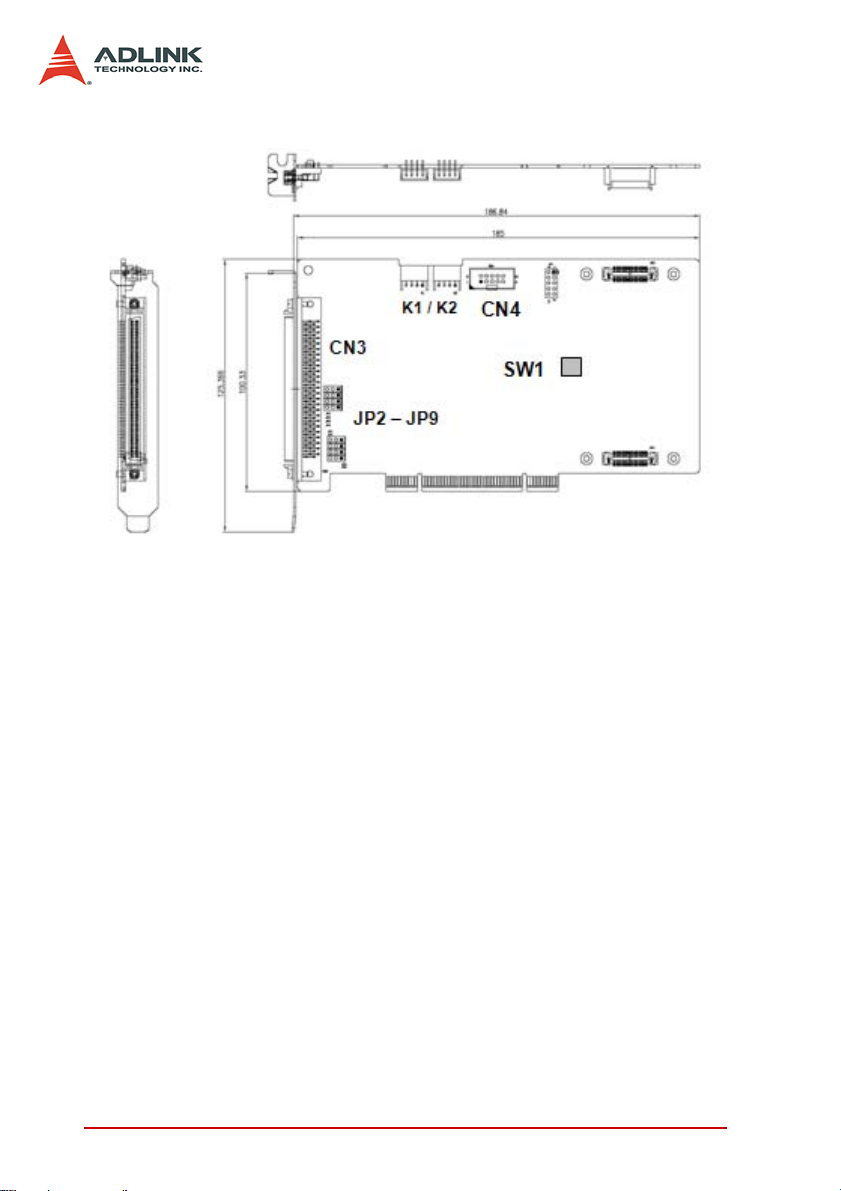
Figure 2-1: PCB Layout of the PCI-8154
X CN3: Input / Output Signal Connector (100-pin)
X K1 / K2: Simultaneous Start / Stop Connector
X CN4: Manual Pulsar
X SW1: DIP switch for card index selection (0-15)
X JP2-JP9: Pulse output selection jumper (Line Driver / Open
Collector)
10 Installation
Page 21

2.3 PCI-8154 Hardware Installation
2.3.1 Hardware configuration
The PCI-8154 is fully Plug-and-Play compliant. Hence, memory
allocation (I/O port locations) and IRQ channel of the PCI card are
assigned by the system BIOS. The address assignment is done
on a board-by-board basis for all PCI cards in the system.
2.3.2 PCI slot selection
Some computer system may hav e both PC I and ISA slots. Do not
force the PCI card into a PC/AT slot. The PCI-8154 can be used in
any PCI slot.
2.3.3 Installation Procedures
1. Read through this manual and setup the jumper according to your application
2. Turn off your computer. Turn off all accessories (printer,
modem, monitor, etc.) connected to computer. Remove
the cover from the computer.
3. Select a 32-bit PCI expansion slot. PCI slots are shorter
than ISA or EISA slots and are usually white or ivory.
4. Before handling the PCI-8154, discharge any static
buildup on your body by touching the metal case of the
computer. Hold the edge of the card and do not touch
the components.
5. Position the board into the PCI slot you have selected.
6. Secure the card in place at the rear panel of the system
unit using screws removed from the slot.
2.3.4 Troubleshooting4:
If your system doesn’t boot or if you experience erratic operation
with your PCI board in place, it’s most likely caused by an interrupt
conflict (possibly an incorrect ISA setup). In general, the solution,
once determined it is not a simple oversight, is to consult the BIOS
documentation that comes with your system.
Installation 11
Page 22

Check the control panel of the Windows system if the card is listed
by the system. If not, check the PCI settings in the BIOS or use
another PCI slot.
12 Installation
Page 23

2.4 Software Driver Installation
1. Autorun the ADLINK All-In-One CD. Choose Driver
Installation -> Motion Control -> PCI-8154.
2. Follow the procedures of the installer.
3. After setup installation is completed, rest art windows.
Note: Please download the latest software from ADLINK website if
necessary.
2.5 CN3 Pin Assignments: Main Connector
CN3 is the main connector for the motion control I/O signals.
No. Name I/O Function No. Name I/O Function
1 VDD O +5V power supply output 51 VDD O +5V power supply output
2 EXGND - Ext. power ground 52 EXGND - Ext. power ground
3 OUT0+ O Pulse signal (+) 53 OUT2+ O Pulse signal (+)
4 OUT0- O Pulse signal (-) 54 OUT2- O Pulse signal (-)
5 DIR0+ O Dir. signal (+) 55 DIR2+ O Dir. signal (+)
6 DIR0- O Dir. signal (-) 56 DIR2- O Dir. signal (-)
7 SVON0 O Servo On/Off 57 SVON2 O Servo On/Off
8 ERC0 O Dev. ctr, clr. Signal 58 ERC2 O Dev. ctr, clr. signal
9 ALM0 I Alarm signal 59 ALM2 I Alarm signal
10 INP0 I In-position signal 60 INP2 I In-position signal
11 RDY0 I Multi-purpose Input signal 61 RDY2 I Multi-purpose Input signal
12 EXGND Ext. power ground 62 EXGND Ext. power ground
13 EA0+ I Encoder A-phase (+) 63 EA2+ I Encoder A-phase (+)
14 EA0- I Encoder A-phase (-) 64 EA2- I Encoder A-phase (-)
15 EB0+ I Encoder B-phase (+) 65 EB2+ I Encoder B-phase (+)
16 EB0- I Encoder B-phase (-) 66 EB2- I Encoder B-phase (-)
17 EZ0+ I Encoder Z-phase (+) 67 EZ2+ I Encoder Z-phase (+)
18 EZ0- I Encoder Z-phase (-) 68 EZ2- I Encoder Z-phase (-)
19 VDD O +5V power supply output 69 VDD O +5V power supply output
20 EXGND - Ext. power ground 70 EXGND - Ext. power ground
21 OUT1+ O Pulse signal (+) 71 OUT3+ O Pulse signal (+)
22 OUT1- O Pulse signal (-) 72 OUT3- O Pulse signal (-)
23 DIR1+ O Dir. signal (+) 73 DIR3+ O Dir. signal (+)
24 DIR1- O Dir. signal (-) 74 DIR3- O Dir. signal (-)
Table 2-1: CN3 Pin Assignments: Main Connector
Installation 13
Page 24

No. Name I/O Function No. Name I/O Function
25 SVON1 O Servo On/Off 75 SVON3 O Servo On/Off
26 ERC1 O Dev. ctr, clr. Signal 76 ERC3 O Dev. ctr, clr. signal
27 ALM1 I Alarm signal 77 ALM3 I Alarm signal
28 INP1 I In-position signal 78 INP3 I In-position signal
29 RDY1 I Multi-purpose Input signal 79 RDY3 I Multi-purpose Input signal
30 EXGND Ext. power ground 80 EXGND Ext. power ground
31 EA1+ I Encoder A-phase (+) 81 EA3+ I Encoder A-phase (+)
32 EA1- I Encoder A-phase (-) 82 EA3- I Encoder A-phase (-)
33 EB1+ I Encoder B-phase (+) 83 EB3+ I Encoder B-phase (+)
34 EB1- I Encoder B-phase (-) 84 EB3- I Encoder B-phase (-)
35 EZ1+ I Encoder Z-phase (+) 85 EZ3+ I Encoder Z-phase (+)
36 EZ1- I Encoder Z-phase (-) 86 EZ3- I Encoder Z-phase (-)
37 PEL0 I End limit signal (+) 87 PEL2 I End limit signal (+)
38 MEL0 I End limit signal (-) 88 MEL2 I End limit signal (-)
39 GDI0 I DI/LTC/PCS/SD/CLR0 89 GDI2 I DI/LTC/PCS/SD/CLR2
40 DO0 O General Output 0 90 DO2 O General Output 2
41 ORG0 I Origin signal 91 ORG2 I Origin signal
42 EXGND Ext. power ground 92 EXGND Ext. power ground
43 PEL1 I End limit signal (+) 93 PEL3 I End limit signal (+)
44 MEL1 I End limit signal (-) 94 MEL3 I End limit signal (-)
45 GDI1 I DI/LTC/PCS/SD/CLR1/EMG 95 GDI3 I DI/LTC/PCS/SD/CLR3
46 DO1 O General Output 1 96 DO3 O General Output 3
47 ORG1 I Origin signal 97 ORG3 I Origin signal
48 EXGND - Ext. power ground 98 EXGND - Ext. power ground
49 EXGND - Ext. power ground 99 E_24V - Isolation power Input, +24V
50 EXGND - Ext. power ground 100 E_24V - Isolation power Input, +24V
Table 2-1: CN3 Pin Assignments: Main Connector
14 Installation
Page 25
2.6 K1/K2 Pin Assignments: Simultaneous Start/ Stop
K1 and K2 are for simultaneous st ar t/stop signals for mu ltiple axes
or multiple cards.
No. Name Function
1 +5V PCI Bus power Output (VCC)
2 S TA Simultaneous start signal input/output
3 STP Simultaneous stop signal input/output
4 GND PCI Bus power ground
T able 2-2: K1/K2 Pin Assignments: Simultaneous Start/Stop
Note: +5V and GND pins are provided by the PCI Bus power.
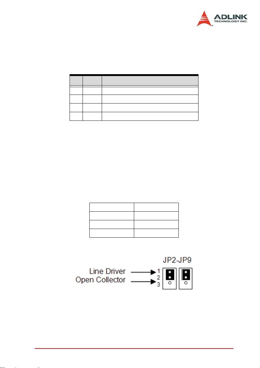
2.7 JP2 to JP9 Jumper Setting for Pulse Output
JP2-JP9 are used to set the type of pulse output signals (DIR and
OUT). The output signal type can either be differential line driver
or open collector output. Refer to section 3.1 for detail jumper settings. The default setting is differential line driver mode. The mapping table is as follows:
JP6 & JP7 Axis 0
JP4 & JP5 Axis 1
JP8 & JP9 Axis 2
JP2 & JP3 Axis 3
Installation 15
Page 26

2.8 SW1 Card Index Selection
The SW1 switch is used to set the card index. For example, if 1 is
set to ON and the others are OFF, that card index is 1. The index
value can be from 0 to 15. Refer to the following table for details.
Card ID Switch Sett ing (ON=1)
00000
10001
20010
30011
40100
50101
60110
70111
81000
91001
10 1010
11 1011
12 1100
13 1101
14 1110
15 1111
T able 2-3: SW1 Card Index
16 Installation
Page 27

2.9 CN4 Manual Pulsar
The signals on CN4 are for manual pulsar input.
No. Name Function (Axis)
1 VDD Isolated Power +5V
2 PA+ Pulser A+ pha se signal input
3 PA- Pulser A-phase signal input
4 PB+ Pulser B+ phase signal input
5 PB- Pulser B-phase signal input
6 EXGND External Ground
7 N/A Not Available
8 N/A Not Available
9 N/A Not Available
T able 2-4: CN4 Manual Pulsar
Note: The +5V and GND pins are directly given by the PCI-bus
power. Therefore, these signals are not isolated.
Installation 17
Page 28

18 Installation
Page 29

3 Signal Connections
Signal connections of all I/O’s are described in this chapter. Refer
to the contents of this chapter before wiring a ny cable between the
PCI-8154 and any motor driver.
This chapter contains the following sections:
Section 3.1 Pulse Output Signals OUT and DIR
Section 3.2 Encoder Feedback Signals EA, EB and EZ
Section 3.3 Orig in Sign al ORG
Section 3.4 End- Lim it Signa ls PEL an d MEL
Section 3.5 In-position signals INP
Section 3.6 Alarm sign al ALM
Section 3.7 Devia tio n coun te r clea r signal ERC
Section 3.8 general-purpose signals SVON
Section 3.9 Gen e ra l-p ur po se s ign al RDY
Section 3.10 Multifunction output pin: DO/CMP
Section 3.11 Multifunction input signal DI/LTC/SD/PCS/CLR/EMG
Section 3.12 Pulse input signals PA and PB
Section 3.13 Simultaneous start/stop signals STA and STP
Signal Connections 19
Page 30

3.1 Pulse Output Signals OUT and DIR
There are 4 axes pulse output signals on the PCI-8154. For each
axis, two pairs of OUT and DIR differential signals are used to
transmit the pulse train and indicate the direction. The OUT and
DIR signals can also be programmed as CW and CCW signal
pairs. Refer to section 4.1.1 for details of the logical characteristics
of the OUT and DIR signals. In this section, the electrical charac teristics of the OUT and DIR signals are detailed. Each signal consists of a pair of differential signals. For example, OUT0 consists
of OUT0+ and OUT0- signals. The following table shows all pulse
output signals on CN3.
CN3 Pin No. Signal Name Description Axis #
3 OUT0+ Pulse signals (+) 0
4 OUT0- Pulse signals (-) 0
5 DIR0+ Direction signal (+) 0
6 DIR0- Direction signal (-) 0
21 OUT1+ Pulse signals (+) 1
22 OUT1- Pulse signals (-) 1
23 DIR1+ Direction signal (+) 1
24 DIR1- Direction signal (-) 1
53 OUT2+ Pulse signals (+) 2
54 OUT2- Pulse signals (-) 2
55 DIR2+ Direction signal (+) 2
56 DIR2- Direction signal (-) 2
71 OUT3+ Pulse signals (+) 3
72 OUT3- Pulse signals (-) 3
73 DIR3+ Direction signal (+) 3
74 DIR3- Direction signal (-) 3
The output of the OUT or DIR signals can be configured by jumpers as either differential line driver s or open collector outp ut. Users
20 Signal Connections
Page 31

can select the output mode either by jumper wiring between 1 and
2 or 2 and 3 of jumpers JP2-JP9 as follows:
For differential line driver
Output Signal
OUT0+ JP6 JP6
DIR0+ JP7 JP7
OUT1+ JP4 JP4
DIR1+ JP5 JP5
OUT2+ JP9 JP9
DIR2+ JP8 JP8
OUT3+ JP3 JP3
DIR3+ JP2 JP2
output, close breaks
between 1 and 2 of:
For open collector out-
put, close breaks
between 2 and 3 of:
The default setting of OUT and DIR is set to differential line driver
mode.
The following wiring diagram is for OUT and DIR signals of axis.
PCI-8154:
NOTE: If the pulse output is set to open collector output mode,
OUT- and DIR- are used to transmit OUT and DIR signals. The
sink current must not exceed 20mA on the OUT- and DIR- pins.
The default setting is 1-2 shorted.
Signal Connections 21
Page 32

Suggest Usage: Jumper 2-3 shorted and connect OUT-/DIR- to a
470 ohm pulse input interface’s COM of driver. See the following
figure. Choose OUT-/DIR- to connect to driver’s OUT/DIR.
Warning: The sink current must not exceed 20mA or the 26LS31
will be damaged!
22 Signal Connections
Page 33

3.2 Encoder Feedback Signals EA, EB and EZ
The encoder feedback signals include EA, EB, and EZ. Every axis
has six pins for three differential pairs of phase-A (EA), phase-B
(EB), and index (EZ) inputs. EA and EB are used for position
counting, and EZ is used for zero position indexing. Its relative signal names, pin numbers, and axis numbers are shown in the following tables:
CN3 Pin No Signal Name Axis # CN3 Pin No Signal Name Axis #
13 EA0+ 0 14 EA0- 0
15 EB0+ 0 16 EB0- 0
31 EA1+ 1 32 EA1- 1
33 EB1+ 1 34 EB1- 1
63 EA2+ 2 64 EA2- 2
65 EB2+ 2 66 EB2- 2
81 EA3+ 3 82 EA3- 3
83 EB3+ 3 84 EB3- 3
CN3 Pin No Signal Name Axis # CN3 Pin No Signal Name Axis #
17 EZ0+ 0 18 EZ0- 0
35 EZ1+ 1 36 EZ1- 1
67 EZ2+ 2 68 EZ2- 2
85 EZ3+ 3 86 EZ3- 3
The input circuit of the EA, EB, and EZ signals is shown as follows:
Signal Connections 23
Page 34

Please note that the voltage across each differential pair of
encoder input signals (EA+, EA-), (EB+, EB-), and (EZ+, EZ-)
should be at least 3.5V. Therefore, the output current must be
observed when connecting to the encoder feedback or motor
driver feedback as not to over drive the source. The differential
signal pairs are converted to digital signals EA, EB, and EZ; then
feed to the motion control ASIC.
Below are examples of connecting the input signals with an external circuit. The input circuit can be connected to an encoder or
motor driver if it is equipped with: (1) a differential line driver or (2)
an open collector output.
Connection to Line Driver Output
To drive the PCI-8154 encoder input, the driver output must provide at least 3.5V across the differential pairs with at least 8mA
driving capacity. The grounds of both sides must be tied together.
The maximum frequency is 3Mhz or more depends on wiring distance and signal conditioning.
24 Signal Connections
Page 35

Connection to Open Collector Output
To connect with an open collector output, an external power supply is necessary. Some motor drivers can provide the power
source. The connection between the PCI-8154, encoder, and the
power supply is shown in the diagram below . Note that an external
current limiting resistor R is necessary to protect the PCI-8154
input circuit. The following table lists the suggested resistor values
according to the encoder power supply.
Encoder Power (V) External Resistor R
I
= 8mA
f
+5V
+12V
+24V
0
Ω (None)
1.5kΩ
3.0kΩ
For more operation information on the encoder feedback signals,
refer to section 4.4.
Signal Connections 25
Page 36

3.3 Origin Signal ORG
The origin signals (ORG0-ORG3) are used as input signals for the
origin of the mechanism. The following table lists signal names,
pin numbers, and axis numbers:
CN3 Pin No Signal Name Axis #
41 ORG0 0
47 ORG1 1
91 ORG2 2
97 ORG3 3
The input circuit of the ORG signals is shown below. Usually, a
limit switch is used to indicate the origin on one axis. The specifications of the limit switch should have contact capacity of +24V @
6mA minimum. An internal filter circuit is used to filter out any high
frequency spikes, which may cause errors in the operation.
When the motion controller is operated in the home return mode,
the ORG signal is used to inhibit the control output signals (OUT
and DIR). For detailed operations of the ORG signal, refer to section 4.3.3.
26 Signal Connections
Page 37

3.4 End-Limit Signals PEL and MEL
There are two end-limit signals PEL and MEL for each axis. PEL
indicates the end limit signal is in the plus direction and ME L indicates the end limit signal is in the minus direction. The signal
names, pin numbers, and axis numbers are shown in the table
below:
CN3 Pin No Signal Name Axis # CN3 Pin No Signal Name Axis #
37 PEL0 0 38 MEL0 0
43 PEL1 1 44 MEL1 1
87 PEL2 2 88 MEL2 2
93 PEL3 3 94 MEL3 3
A circuit diagram is shown in the diagram below. The external limit
switch should have a contact capacity of +24V @ 8mA minimum.
Either ‘A-type’ (normal open) contact or ‘B- type’ (normal closed)
contact switches can be used. To set the active logic of the external limit signal, please refer to the explanation of
_8154_set_limit_logic function.
Signal Connections 27
Page 38

3.5 In-position Signal INP
The in-position signal INP from a servo motor driver indicates its
deviation error. If there is no deviation error then the servo’s position indicates zero. The signal names, pin numbers, and axis
numbers are shown in the table below:
CN3 Pin No Signal Name Axis #
10 INP0 0
28 INP1 1
60 INP2 2
78 INP3 3
The input circuit of the INP signals is shown in the diagram below:
The in-position signal is usually generated by the servomotor
driver and is ordinarily an open collector output signal. An external
circuit must provide at least 8mA current sink capabilities to drive
the INP signal.
28 Signal Connections
Page 39

3.6 Alarm Signal ALM
The alarm signal ALM is used to indicate the ala rm status from the
servo driver. The signal names, pin numbers, and axis numbers
are shown in the table below:
CN3 Pin No Signal Name Axis #
9ALM00
27 ALM1 1
59 ALM2 2
77 ALM3 3
The input alarm circuit is shown below. The ALM signal usually is
generated by the servomotor driver and is ordinarily an open collector output signal. An external circuit must provide at least 8mA
current sink capabilities to drive the ALM signal.
Signal Connections 29
Page 40

3.7 Deviation Counter Clear Signal ERC
The deviation counter clear signal (ERC) is active in the following
4 situations:
1. Home return is complete
2. End-limit switch is active
3. An alarm signal stops OUT and DIR signals
4. An emergency stop command is issued by software
(operator)
The signal names, pin numbers, and axis numbers are shown in
the table below:
CN3 Pin No Signal Name Axis #
8 ERC0 0
26 ERC1 1
58 ERC2 2
76 ERC3 3
The ERC signal is used to clear the deviation counter of the se rvomotor driver. The ERC output circuit is an open collector with a
maximum of 35V at 50mA driving capacity.
30 Signal Connections
Page 41

3.8 General-purpose Signal SVON
The SVON signal can be used as a servomotor-on control or general purpose output signal. The signal names, pin numbers, and
its axis numbers are shown in the following table:
CN3 Pin No Signal Name Axis #
7SVON00
25 SVON1 1
57 SVON2 2
75 SVON3 3
The output circuit for the SVON signal is shown below:
Signal Connections 31
Page 42

3.9 General-purpose Signal RDY
The RDY signals can be used as motor driver ready input or general purpose input signals. The signal names, pin numbers, and
axis numbers are shown in the following table:
CN3 Pin No Signal Name Axis #
11 RDY0 0
29 RDY1 1
61 RDY2 2
79 RDY3 3
The input circuit of RDY signal is shown in the following diagram:
32 Signal Connections
Page 43

3.10 Multi-Functional output pin: DO/CMP
The PCI-8154 provides 4 multi-functional output channels: DO0/
CMP0 to DO3/CMP3 corresponds to 4 axes. Each of the output
pins can be configured as Digit Output (DO) or as Comparison
Output (CMP) individually. When configured as a Comparison Output pin, the pin will generate a pulse signal when the encoder
counter matches a pre-set value set by the user.
The multi-functional channels are located on CN3. The signal
names, pin numbers, and axis numbers are shown below:
CN3 Pin No Signal Name Axis #
40 DO/CMP0 0
46 DO/CMP1 1
90 DO/CMP2 2
96 DO/CMP3 3
The following wiring diagram is of the CMP on the first 2 axes:
Signal Connections 33
Page 44

3.11 Multi-Functional input pin: DI/LTC/SD/PCS/CLR/ EMG
The PCI-8154 provides 4 multi-functional input pins. Each of the 4
pins can be configured as DI (Digit Input) or LTC (Latch) or SD
(Slow down) or PCS (Target position override) or CLR (Counter
clear) or EMG (Emergency). To select the pin function, please
refer to 6.12.
The multi-functional input pins are on CN3. The signal names, pin
numbers, and axis numbers are shown in the following table:
CN3 Pin No Signal Name Axis #
39 DI/LTC/SD/PCS/CLR/EMG_0 0
45 DI/LTC/SD/PCS/CLR/EMG_1 1
89 DI/LTC/SD/PCS/CLR/EMG_2 2
95 DI/LTC/SD/PCS/CLR/EMG_3 3
The multi-functional input pin wiring diagram is as follows:
34 Signal Connections
Page 45

3.12 Pulser Input Signals PA and PB (PCI-8154)
The PCI-8154 can accept differential pulser input signals through
the pins of CN4 listed below. The pulser behaves like an encoder.
The A-B phase signals generate the positio ning info rmation, wh ich
guides the motor.
CN4 Pin No Signal Name Axis # CN4 Pin No Signal Name Axis #
2PA+0-33PA-0-3
4 PB+ 0-3 5 PB- 0-3
The pulser signals are used for Axis 0 to Axis 3. User can decide
to enable or disable each axis pulser with
_8154_disable_pulser_input function.
The wiring diagram of the differential pulser input pins are as followed.
Signal Connections 35
Page 46

3.13 Simultaneously Start/Stop Signals STA and STP
The PCI-8154 provides STA and STP signals, which enable simultaneous start/stop of motions on multiple axes. The STA and STP
signals are on K1/K2.
The STP and STA signals are both input and output signals. To
operate the start and stop action simultaneously, both software
control and external control are needed. With software control, the
signals can be generated from any one of the PCI-8154. Users
can also use an external open collector or switch to drive the STA/
STP signals for simultaneous start/stop.
If there are two or more PCI-8154 cards, connect the K2 conne ctor
on the previous card to K1 connector on the following card. The
K1 and K2 connectors on a same PCI-8154 are connected internally.
You can also use external start and stop signals to issue a crosscard simultaneous motor operation. Just connect external start
36 Signal Connections
Page 47

and stop signals to STA and STP pins on the K1 connector of the
first PCI-8154 card.
Signal Connections 37
Page 48

38 Signal Connections
Page 49

4 Operation Theory
This chapter describes the detail operation of the motion controller
card. Contents of the following sections are as follows:
Section 4.1: Classifications of Motion Controller
Section 4.2: Motion Control Modes
Section 4.3: M ot or Drive r Int er face
Section 4.4: M ec ha n ical switch Interface
Section 4.5: T he Cou n ter s
Section 4.6: The Comparators
Section 4.7: Other Motion Functions
Section 4.8: Interrupt Control
Section 4.9: Multiple Cards Operation
4.1 Classifications of Motion Controller
When motor/stepper control first started, motion control was
widely discussed instead of motor control. Motor control was separated into two layers: motor control and motion control. Motor control relates to PWM, power stage, closed loop, hall sensors, vector
space, etc. Motion control relates to speed profile generating, trajectory following, multi-axes synchronizat ion , an d co ordin a ting .
4.1.1 Voltage motion control interface
The interfaces between motion and motor control are changing
rapidly. Early on, a voltage singal was used as a command to the
motor controller. The amplitude of the signal means how fast a
motor is rotating and the time duration of the voltage changes
means how fast a motor acceleration from one speed to the other
speed. Voltage signal as a command to motor driver is so called
“analog” motion controller. It is much eaiser to integrate into an
analog circuit of motor controller; however noise is sometimes a
big problem for this type of motion control. Also, to do positioning
control of a motor, the analog motion controller must ha ve a feedback signal with position information and use a closed loop control
algorithm to make it possible. This increased the complexity of
motion control and not easy to use for a beginner.
Operation Theory 39
Page 50

4.1.2 Pulse motion control interface
The second interface of motion and motor control is a pulse train
type. As a trend of digital world, pulse trains represent a new concept to motion control. The counts of pulses show how many ste ps
of a motor rotates and the frequency of pulses show how fast a
motor runs. The time duration of frequency changes represent the
acceleration rate of a motor. Because of this interface, a servo or
stepper motor can be easier than an analog type for positioning
applications. It means that motion and motor control can be separated more easily by this way.
Both of these two interfaces need to provide for gains tuning. For
analog position controllers, the control loops are built inside and
users must tune the gain from the controller. For pulse type position controllers, the control loops are built outside on the motor
drivers and users must tune the gains on drivers.
For more than one axes’ operation, motion control seems more
important than motor control. In industial applications, reliable is a
very important factor. Motor driver vendors make good performance products and a motion controller vendors make powerful
and variety motion software. Integrated two products make our
machine go into perfect.
4.1.3 Network motion control interface
Recently, there was a new control interface was introduced--a network motion controller. The command between motor driver and
motion controller is not analog or pulses signal any more. It is a
network packet which contents position information and motor
information. This type of controller is more reliable because it is
digitized and packetized. Because a motion controller must be
real-time, the nerowrk must have real-time capacity around a cycle
time below 1 mini-second. This means that non-commercial networks cannot do this job. It must have a specific network, such as
Mitsubishi SSCNET. The network may also be built with fiberoptics
to increase communication reliability.
40 Operation Theory
Page 51

4.1.4 Software real-time motion control kernel
For motion control kernel, there are three ways to accomplish it:
DSP, ASIC, and software real-time.
A motion control system needs an absolutely real-time control
cycle and the calculation on controller must provide a control data
at the same cycle. If not, the motor will not run smoothly. Many
machine makers will use PC’s computing power to do this. A feedback counter card can simply be used and a voltage output or
pulse output card to make it. This method is very low-end and
takes much software effort. For sure their realtime performance,
they will use a real-time software on the system. It increases the
complexity of the system too. But this method is the most flexible
way for a professional motion control designers. Most of these
methods are on NC machines.
4.1.5 DSP motion control kernel
A DSP-based motion controller kernel solves real-time software
problem on computer. DSP is a micro-processer itself and all
motion control calculations can be done on it. There is no real-time
software problem because DSP has its own OS to arrange all the
procedures. There is no interruption from other inputs or context
switching problem like Windows based computer. Although it has
such a perfect performance on real-time requirements, its calculation speed is not as fast as PC’s CPU at this age. The software
interfacing between DSP controller’s vendors and users is not
easy to use. Some controller vendors provide some kind of
assembly languages for users to learn and some controller vendors provide only a handshake documents for users to use. Both
ways are not easy to use. DSP based controller provide a bette r
way than software kernel for machine makers to build they applications.
4.1.6 ASIC motion control kernel
An ASIC motion control kernel is falls between software kernel
and DSP kernel in terms of difficulty. It has no real-time problem
because all motion functions are done via the ASIC. Users or controller’s vendors just need to set some parameters which the ASIC
requires and the motion control will be done easily. This kind of
Operation Theory 41
Page 52

motion control separates all system integration problems into 4
parts: Motor driver’s performance, ASIC outputting profile, vendor’s software parameters to the ASIC, and users’ command to
vendors’ software. It makes motion controller co-operated more
smoothly between devices.
4.1.7 Compare Table of all motion control types
Software ASIC DSP
Price Fair Cheap Expensive
Functionality Highest Low Normal
Maintenance Hard Easy Fair
Analog Pulses Network
Price High Low Normal
Signal Quality Fair Good Reliable
Maintenance Hard Easy Easy
4.1.8 PCI-8154 motion controller type
The PCI-8154 is ASIC based, pulse type motion controller made
into three blocks: motion ASIC, PCI card, software motion library.
The motion ASIC can be accessed via our software motion libra y
under many kinds of Windows NT/2000/XP, Linux, and RTX driver.
Our software motion library provides one-stop-function for controlling motors. All the speed parameter calculations are done via our
library.
For example, to perform a one-axis point to point moition with a
trapezoidal speed profile, only fill the target position, speed, and
acceleration time in one function. Then the motor will run as the
profile. It takes no CPU resources because every control cycle
pulse generation is done by the ASIC. The precision of target position depends on motor drivers’ closed loop control performance
and mechnical parts, not on motion controller’s command because
the motion controller is only responsible for sending correct pulses
counts via a desired speed profile. So it is much e asier for programmers, mechnical or electrical engineers to find out problems.
42 Operation Theory
Page 53

4.2 Motion Control Modes
Motion control makes the motors run according to a specific speed
profile, path trajectory and synchronous condition with other axes.
The following sections describe the motion control modes of this
motion controller could be performed.
4.2.1 Coordinate system
The Cartesian coordinate is used and pulses are in the unit of
length. The physical length depends on mechanical parts and
motor’s resolution. For example, if a motor is on a screw ball, and
the pitch of screw ball is 10mm and the pulses needed for a round
of motor are 10,000 pulses. One pulse’s physical unit is equal to
10mm/10,000p =1 mm.
Just set a command with 15,000 pulses for motion controller if we
want to move 15mm. How about if we want to move 15.0001mm?
Simple! The motion controller will keep the residue value less
than 1 pulse and add it to next command.
The motion controller sends incremental pulses to motor drive rs. It
means that we can only send relative command to motor driver.
But we can solve this problem by calculating the difference
between current position and target position first. Then send the
differences to motor driver. For example, if current position is 1000
and we want to move a motor to 9000, you can use an absolute
command to set a target position of 9000. Inside the motion controller, it will get current position 1000 first then calculate the difference from target position. The result is +8000. So, the motion
controller will send 8000 pulses to motor driver to move the position of 9000.
Sometimes, users need to install a linear scale or external
encoder to check machine’s position. But how do you to build this
coordinate system? If the resolution of external encoder is 10,000
Operation Theory 43
Page 54

pulses per 1mm and the motor will move 1mm if the motion controller send 1,000 pulses, It means that when we want to move 1
mm, we need to send 1,000 pulses to motor driver then we will get
the encoder feedback value of 10,000 pulses. If we want to use an
absolute command to move a motor to 10,000 pulses position and
current position read from encoder is 3500 pulses, how many
pulses will it send to motor driver? The answer is (10000 – 3500 ) /
(10,000 / 1,000)=650 pulses. The motion controller will calculate it
automatically if users set “move ratio” already. The “move ratio”
means the (feedback resolution/command resolution).
4.2.2 Absolute and relative position move
In the coordinate system, we have two kinds command for users
to locate the target position. One is absolute and the other is relative. Absolute command means that user give the motion controller a position, then the motion controller will move a motor to that
position from current position. Relative command means that user
give the motion controller a distance, then the motion controller
will move motor by the distance from current position. During the
movement, users can specify the speed profile. It means user can
define how fast and at what speed to reach the position.
44 Operation Theory
Page 55

4.2.3 Trapezoidal speed profile
Trapezodial speed profile means the acceleration/deceleration
area follows a 1st order linear velocity profile (constant acceleration rate). The profile chart is shown as below:
The area of the velocity profile represents the distance of this
motion. Sometimes, the profile looks like a triangle because the
desired distance from user is smaller than the area of given speed
parameters. When this situation happens, the motion controller
will lower the maximum velocity but keep the acceleration rate to
meet user’s distane requirement. The chart of this situation is
shown as below:
This kind of speed profile could be applied on velocity mode, position mode in one axis or multi-axes linear interpolation and two
axes circular interpolation modes.
Operation Theory 45
Page 56

4.2.4 S-curve and Bell-curve speed profile
S-curve means the speed profile in accelerate/decelerate area follows a 2nd order curve. It ca n reduce vibration at the beginning of
motor start and stop. In order to speed up the acceleration/deceleration during motion, we need to insert a linear part into these
areas. We call this shape as “Bell” curve. It adds a linear curve
between the upper side of s-curve and lower side of s-curve. This
shape improves the speed of acceleration and also reduces the
vibration of acceleration.
For a bell curve, we define its shape parameters as below:
X Tacc: Acceleration time in second
X Tdec: Deceleration time in second
X StrVel: Starting velocity in PPS
X MaxVel: Maximum velocity in PPS
X VSacc: S-curve part of a bell curve in deceleration in PPS
X VSdec: S-curve part of a bell curve in deceleration in PPS
46 Operation Theory
Page 57

If VSacc or VSdec=0, it means acceleration or deceleration use
pure S-curve without linear part. The Acceleration chart of bell
curve is shown below:
The S-curve profile motion functions are designed to always produce smooth motion. If the time for acceleration parameters combined with the final position don’t allow an axis to reach the
maximum velocity (i.e. the mov ing distance is too small to reach
MaxVel), then the maximum velocity is automatically lowered (see
the following Figure).
The rule is to lower the value of MaxVel and the Tacc, Tdec,
VSacc, VSdec automatically, and keep StrVel, acceleration, and
jerk unchanged. This is also applicable to Trapezoidal profile
motion.
This kind of speed profile could be applied on velocity mode, position mode in one axis or multi-axes linear interpolation and two
axes circular interpolation modes.
Operation Theory 47
Page 58

4.2.5 Velocity mode
Veloctiy mode means the pulse command is continuously outputing until a stop command is issued. The motor will run without a
target position or desired distance unless it is stopped by other
reasons. The output pulse accelerates from a starting velocity to a
specified maximum velocity. It can be follow a linear or S-curve
acceleration shape. The pulse output rate is kept at maximum
velocity until another velocity command is set or a stop command
is issued. The velocity could be overrided by a new speed setting.
Notice that the new speed could not be a reversed speed of original running speed. The speed profile of this kind of motion is
shown as below:
48 Operation Theory
Page 59

4.2.6 One axis position mode
Position mode means the motion controller will output a specific
amount of pulses which is equal to users’ desired position or distance. The unit of distance or position is pulse internally on the
motion controller. The minimum length of distance is one pulse.
However, in PCI-8154, we provide a floating point function for
users to transform a physical length to pulses. Inside our software
library, we will keep those distance less than one pulse in register
and apply them to the next motion function. Besides positioning
via pulse counts, our motion controller provides three types of
speed profile to accomplish positioning. There are 1st order trapezoidal, 2nd order S-curve, and mixed bell curve. Users can call
respective functions to perform that. The following char shows the
relationship between distance and speed profile. We use trapezoidal shape to show it.
The distance is the area of the V-t diagram of this profile.
Operation Theory 49
Page 60

4.2.7 Two axes linear interpolation position mode
“Interpolation between multi-axes” means these axes start simultaneously, and reach their ending points at the same time. Linear
means the ratio of speed of every axis is a constant value.
Assume that we run a motion from (0,0) to (10,4). The linear interpolation results are shown as below.
The pulses output from X or Y axis remains 1/2 pulse difference
according to a perfect linear line. The precision of linear interpolation is shown as below:
If users want to stop an interpolation group, just call a stop function on first axis of the group.
As in the diagram below, 4-axis linear interpo lation means to move
the XY position from P0 to P1. The 2 axes start and stop simultaneously, and the path is a straight line.
50 Operation Theory
Page 61

The speed ratio along X-axis and Y-axis is (ΔX: ΔY), respectively,
and the vector speed is:
When calling 4-axis linear interpolation functions, the ve ctor speed
needs to define the start velocity, StrVel, and maximum velocity,
MaxVel.
4.2.8 Two axes circular interpolation mode
Circular interpolation means XY axes simultaneously start from initial point, (0,0) and stop at end point, (1800,600). The path
between them is an arc, and the MaxVel is the tangential speed.
Notice that if the end point of arc is not at a proper position, it will
move circularly without stopping.
Y
(1800,600)
(0,0)
Center
(1000,0)
X
The motion controller will move to the final point user desired even
this point is not on the path of arc. But if the final point is not at the
location of the shadow area of the following graph, it will run circularly without stopping.
Operation Theory 51
Page 62

The command precision of circular interpolation is shown below.
The precision range is at radius ±1/2 pulse.
4.2.9 Continuous motion
Continuous motion means a series of motion command or po sition
can be run continuously. Users can set a new command right after
previous one without interrupting it. The motion controller can
make it possible because there are three command buffers (preregisters) inside.
When first command is executing, users can set second command
into first buffer and third command into second buffer. Once the
first command is finished, the motion controller will push the second command to the executing register and the third command to
first buffer. Now, the second buffer is empty and user can set the
4th command into 2nd buffer. Normally, if users have enough time
52 Operation Theory
Page 63

to set a new command into 2nd buffer before executing register is
finished, the motion can run endlessly. The following diagram
shows this architecture of continuous motion.
Besides position command, the speed command should be set
correctly to perform a speed continuous profile. For the following
example, there are three motion command of this continuous
motion. The second one has high speed than the others. The
interconnection of speed between these three motion functions
should be set as the following diagram:
Operation Theory 53
Page 64

If the 2nd command’s speed value is lower than the others, the
settings would be like as following diagram:
For 4-axis continuous arc interpolation is the same concept. You
can set the speed matched between two command speed settings.
If the INP checking is enabled, the motion will have some delayed
between each command in buffers. INP check enabled make the
desired point be reached but reduce the smoothing between each
command. If users don’t need this delay and need the smoothing,
please turn INP checking off.
54 Operation Theory
Page 65

4.2.10 Home Return Mode
Home return means searching a zero position point on the coordinate. Sometimes, users use a ORG, EZ or EL pin as a zero position on the coordinate. At the beginning of machine power on, the
program needs to find a zero point of this machine. Our motion
controller provides a home return mode to make it.
We have many home modes and each mode contents many control phases. All of these phases are done by ASIC. No software
efforts or CPU loading will be taken. After home return is finished,
the target counter will be reset to zero at the desired condition of
home mode. For example, a raising edge when ORG input. Sometimes, the motion controller will still output pulses to make
machine show down after resetting the counter. When the motor
stops, the counter may not be at zero po int but the home return
procedure is finished. The counter value you see is a reference
position from machine’s zero point already.
The following figures show the various home modes: R means
counter reset ( command and position counter ). E means ERC
signal output.
Operation Theory 55
Page 66

Home mode=0: ( ORG Turn ON then reset counter )
X When SD is not installed
X When SD is installed and SD is not latched
56 Operation Theory
Page 67

Home mode=1: (Twice ORG turn ON then reset counter)
Home mode=2: (ORG ON then Slow down to count EZ numbers and reset counter)
Operation Theory 57
Page 68

Home mode=3: (ORG ON then count EZ numbers and reset
counter)
Home mode=4: (ORG On then reverse to count EZ number
and reset counter)
58 Operation Theory
Page 69

Home mode=5: (ORG On then reverse to count EZ number
and reset counter, not using FA Speed)
Home mode=6: (EL On then reverse to leave EL and reset
counter)
Home mode=7: (EL On then reverse to count EZ number and
reset counter)
Operation Theory 59
Page 70

Home mode=8: (EL On then reverse to count EZ number and
reset counter, not using FA Speed)
Home mode=9: (ORG On then reverse to zero position, an
extension from mode 0)
60 Operation Theory
Page 71

Home mode=10: (ORG On then counter EZ and reverse to
zero position, an extension from mode 3)
Home mode=11: (ORG On then reverse to counter EZ and
reverse to zero position, an extension from mode 5)
Operation Theory 61
Page 72

Home mode=12: (EL On then reverse to count EZ numbe r a nd
reverse to zero position, an extension from mode 8)
4.2.11 Home Search Function
This mode is used to add auto searching function on normal home
return mode described in previous section no matter which position the axis is. The following diagram is shown the example for
home mode 2 via home search fu nction. The OR G offset can’t be
zero. Suggested value is the double length of ORG area.
62 Operation Theory
Page 73

4.2.12 Manual Pulser Function
Manual pulser is a device to generate pulse trains by hand. The
pulses are sent to motion controller and re-directed to pulse outp ut
pins. The input pulses could be multiplied or divided before sending out.
The motion controller receives two kinds of pulse trains from manual pulser device: CW/CCW and AB phase. If the AB phase input
mode is selected, the multiplier has additional selection of 1, 2, or
4.
The following figure shows pulser ratio block diagram.
4.2.13 Simultaneous Start Function
Simultaneous motion means more than one axis can be starte d by
a Simultaneous signal which could be external or internal signals.
For external signal, users must set move parameters first for all
axes then these axes will wait an extern start/stop command to
start or stop. For internal signal, the start command could be from
a software start function. Once it is issued, all axes which are in
waiting synchronous mode will start at the same time.
Operation Theory 63
Page 74

4.2.14 Speed Override Function
Speed override means that users can change command’s speed
during the operation of motion. The change parameter is a percentage of original defined speed. Users can define a 100% sp eed
value then change the speed by percentage of original speed
when motion is running. If users didn’t define the 100% speed
value. The default 100% speed is the latest motion command’s
maximum speed. This function can be applied on any motion function. If the running motion is S-curve or bell curve, the speed override will be a pure s-curve. If the running motion is t-curve, the
speed override will be a t-curve.
64 Operation Theory
Page 75

4.2.15 Position Override Function
Position override means that when users issue a positioning command and want to change its target position during this operation.
If the new target position is behind current position when override
command is issued, the motor will slow down then reverse to new
target position. If the new target position is far away from current
position on the same direction, the motion will remain its speed
and run to new target position. If the override timing is on the
deceleration of current motion and the target position is far away
from current position on the same direction, it will accelerate to
original speed and run to new target position. The operation examples are shown as below. Notice that if the new target position’s
relative pulses are smaller than original slow down pulses, this
function can’t work properly.
Operation Theory 65
Page 76

4.3 The motor driver interface
We provide several dedicated I/Os which can be connected to
motor driver directly and have their own functions. Motor drivers
have many kinds of I/O pins for external motion controller to use.
We classify them to two groups. One is pulse I/O signals including
pulse command and encoder interface. The other is digital I/O signals including servo ON, alarm, INP, servo ready, alarm reset and
emergency stop inputs. The following sections will describe the
functions these I/O pins.
4.3.1 Pulse Command Output Interface
The motion controller uses pulse command to control servo/stepper motors via motor drivers. Please set the drivers to position
mode which can accept pulse trains as position command. The
pulse command consists of two signal pairs. It is defined as OUT
and DIR pins on connector. Each signal has two pins as a pair for
differential output. There are two signal modes for pulse output
command: (1) single pulse output mode (OUT/DIR), and (2) dual
pulse output mode (CW/CCW type pulse output). The mode must
be the same as motor driver. The modes vs. signal type of OUT
and DIR pins are listed in the table below:
Mode Output of OUT pin Output of DIR pin
Dual pulse output
(CW/CCW)
Single pulse output
(OUT/DIR)
Pulse signal in plus
(or CW) direction
Pulse signal Direction signal (level)
Pulse signal in minus
(or CCW) direction
66 Operation Theory
Page 77

Single Pulse Output Mode (OUT/DIR Mode)
In this mode, the OUT pin is for outputting command pulse chain.
The numbers of OUT pulse represent distance in pulse. The frequency of the OUT pulse represents speed in pulse per second.
The DIR signal represents command direction of positive (+) or
negative (-). The diagrams below show the output waveform. It is
possible to set the polarity of the pulse chain.
Operation Theory 67
Page 78

Dual Pulse Output Mode (CW/CCW Mode)
In this mode, the waveform of the OUT and DIR pins represent
CW (clockwise) and CCW (counter clockwise) pulse output
respectively. The numbers of pulse represent distance in pulse.
The frequency of the pulse represents speed in pulse per second.
Pulses output from the CW pin makes the motor mo ve in positive
direction, whereas pulse output from the CCW pin makes the
motor move in negative direction. The following diagram shows
the output waveform of positive (+) commands and negative (-)
commands.
The command pulses are counted by a 28-bit command counter.
The command counter can store a value of total pulses outputting
from controller.
68 Operation Theory
Page 79

4.3.2 Pulse feedback input interface
Our motion controller provides one 28-bit up/do wn cou nter of each
axis for pulse feedback counting. This counter is called position
counter. The position counter counts pulses from the EA and EB
signal which have plus and minus pins on connector for differential
signal inputs. It accepts two kinds of pulse types. One is dual
pulses input (CW/CCW mode) and the other is AB phase input.
The AB phase input can be multiplied by 1, 2 or 4. Multiply by 4 AB
phase mode is the most commonly used in incremental encoder
inputs.
For example, if a rotary encoder has 2000 pulses per rotation,
then the counter value read from the position counter will be 8000
pulses per rotation when the AB phase is multiplied by four.
If users don’t use encoder for motion controller, the feedback
source for this counter must be set as pulse command output or
the counter value will always be zero. If it is set as pulse command
output, users can get the position counter value from pulse command output counter because the feedback pulses are internal
counted from command output pulses.
The following diagrams show these two types of pulse feedback
signal.
Operation Theory 69
Page 80

Plus and Minus Pulses Input Mode (CW/CCW Mode)
The pattern of pulses in this mode is the same as the Dual Pulse
Output Mode in the Pulse Command Output section except that
the input pins are EA and EB.
In this mode, pulses from EA pin cause the counter to count up,
whereas EB pin caused the counter to count down.
90° phase difference signals Input Mode (AB phase Mode)
In this mode, the EA signal is a 90° phase leading or lagging in
comparison with the EB signal. “Lead” or “lag ” of phas e difference
between two signals is caused by the turning direction of the
motor. The up/down counter counts up when the phase of EA signal leads the phase of EB signal.
The following diagram shows the waveform.
The index input (EZ) signal is as the zero reference in linear or
rotary encoder. The EZ can be used to define the mechanical zero
position of the mechanism. The logic of signal must also be set
correctly to get correct result.
70 Operation Theory
Page 81

4.3.3 In position signal
The in-position signal is an output signal from motor driver. It tells
motion controllers a motor has been reached a position within a
predefined error. The predefined error value is in-position value.
Most motor drivers call it as INP value. After motion controller
issues a positioning command, the motion busy status will keep
true until the INP signal is ON. Users can disable INP check for
motion busy flag. If it is disabled, the motion busy will be FALSE
when the pulses command is all sent.
4.3.4 Servo alarm signal
The alarm signal is an output signal from motor driver. It tells
motion controller that there has something error inside servo
motor or driver. Once the motion controller receives this signal, the
pulses command will stop sending and the status of ALM signal
will be ON. The reasons of alarm could be servo motor’s over
speed, over current, over loaded and so on. Please check motor
driver’s manual about the details.
The logic of alarm signal must be set correctly. If the alarm logic’s
setting is not the same as motor driver’s setting, the ALM status
will be always ON and the pulse command can never be outputted.
Operation Theory 71
Page 82

4.3.5 Error clear signal
The ERC signal is an output from the motion controller. It tells
motor driver to clear the error counter. The error counter is
counted from the difference of command pulses and feedback
pulses. The feedback position will always have a delay from the
command position. It results in pulse differences between these
two positions at any moment. The differences are shown in error
counter. Motor driver uses the error counter as a basic control
index. The large the error counter value is, the faster the motor
speed command will be set. If the error counter is zero, it means
that zero motor speed command will be set.
At following four situations, the ERC signal will be outputted automatically from motion controller to motor driver in order to clear
error counter at the same time.
1. Home return is complete
2. The end-limit switch is touched
3. An alarm signal is active
4. An emergency stop command is issued
4.3.6 Servo ON/OFF switch
The servo on/off switch is a general digital output signal on motion
controller. We define it as SVON pin on the connector. It can be
used for switching motor driver’s controlling state. Once it is turned
on, the motor will be held because the control loop of driver is
active. Be careful that when the axis is vertically installed and the
servo signal is turned off, the axis will be in uncontrolled state. It
could fall on the ground. Some situations like servo alarm and
emergency signal ON will result in the same trouble.
72 Operation Theory
Page 83

4.3.7 Servo Ready Signal
The servo ready signal is a general digital input on motion controller. It has no relative purpose to motion controller. Users can connect this signal to motor driver’s RDY signal to check if the motor
driver is in ready state. It lets users to check something like the
motor driver’s power has been inputted or not. Or users can connect this pin as a general input for other purpose. It doesn’t affect
motion control.
4.3.8 Servo alarm reset switch
The servo driver will raise an alarm signal if there is something
wrong inside the servo driver. Some alarm situations like servo
motor over current, over speed, over loading and so on. Power
reset can clear the alarm status but users usually don’t want to
power off the servo motor when operating. There is one pin from
servo driver for users to reset the alarm status. Ou r motion controller provides one general output pin for each axis. Users can use
this pin for resetting servo alarm status.
Operation Theory 73
Page 84

4.4 Mechanical switch interface
We provide some dedicated input pins for mechanical switches
like original switch (ORG), plus and minus end-limit switch (±EL),
slow down switch (SD), positioning start switch (PCS), counter
latch switch (LTC), emergency stop input (EMG) and counter
clear switch (CLR). These switches’ response time is very short,
only a few ASIC clock times. There is no real-time problem when
using these signals. All functions are done by motion ASIC. The
software can just do nothing and only need to wait the results.
4.4.1 Original or home signal
Our controller provides one original or home signal for each axis.
This signal is used for defining zero position of this axis. The logic
of this signal must be set properly before doing home procedure.
Please refer to home mode section for details.
4.4.2 End-Limit switch signal
The end-limit switches are usually installed on both ending sides
of one axis. We must install plus EL at the positive position of the
axis and minus EL at the negative position of the axis. These two
signals are for safety reason. If they are installed reversely, the
protection will be invalid. Once the motor’s moving part touches
one of the end-limit signal, the motion controller will stop sending
pulses and output an ERC signal. It can prevent machine crash
when miss operation.
4.4.3 Slow down switch
The slow down signals are used to force the command pulse to
decelerate to the starting velocity when it is active. This signal is
used to protect a mechanical moving part under hig h speed movement toward the mechanism’s limit. The SD signal is effective for
both plus and minus directions.
74 Operation Theory
Page 85

4.4.4 Positioning Start switch
The positioning start switch is used to move a specific position
when it is turned on. The function is shown as below.
4.4.5 Counter Clear switch
The counter clear switch is an input signal which makes the
counters of motion controller to reset. If users need to reset a
counter according to external command, use this pin as controlling
source.
4.4.6 Counter Latch switch
The counter latch switch is an input signal which makes counter
value to be kept into a register when this input active. If users n eed
to know counter value at the active moment of one input, they can
connect this pin to catch that.
4.4.7 Emergency stop input
Our motion controller provides a global digital input for emergency
situation. Once the input is turned on, our motion controller will
stop all axes’ motion immediately to prevent machine’s damage.
Usually, users can connect an emergency stop button to this input
on their machine. We suggest this input as normal closed type for
safety.
Operation Theory 75
Page 86

4.5 The Counters
There are four counters for each axis of this motion controller.
They are described in this section.
X Command position counter: counts the number of output
pulses
X Feedback position counter: counts the number of input
pulses
X Position error counter: counts the error between command
and feedback pulse numbers.
X General purpose counter: The source can b e con fig ured as
command position, feedback position, manual pulser, or half
of ASIC clock.
X Target position recorder: A software-maintained target posi-
tion value of latest motion command.
4.5.1 Command position counter
The command position counter is a 28-bit binary up/down counter.
Its input source is the output pulses from the motion co ntroller. It
provides the information of the current command position. It is
useful for debugging the motion system.
Our motion system is an open loop type. The motor driver receives
pulses from motion controller and drive the motor to move. When
the driver is not moving, we can check this command counter and
see if there is an update value on it. If it is, it means that the pulses
have seen sent and the problem could be on the motor driver. Try
to check motor driver’s pulse receiving counter when this situation
is happened.
The unit of command counter is in pulse. The counter value could
be reset by a counter clear signal or home function completion.
Users can also use a software command counter setting function
to reset it.
76 Operation Theory
Page 87

4.5.2 Feedback position counter
The feedback position counter is a 28-bit binary up/down counter.
Its input source is the input pulses from the EA/EB pins. It counts
the motor position from motor’s encoder output. This counter
could be set from a source of command position for an option
when no external encoder inputs.
The command output pulses and feedback input pulses will not
always be the same ratio in mini-meters. Users must set the ratio if
these two pulses are not 1:1.
Because our motion controller is not a closed-loop type, the feedback position counter is just for reference after motion is moving.
The position closed-loop is done by servo motor driver. If the servo
driver is well tuned and the mechanical parts are well assembled,
the total position error will remain in acceptable range after motion
command is finished.
4.5.3 Command and Feedback error counter
The command and feedback error counter is used to calculate the
error between the command position and the feedback position.
The value is calculated from command subtracting feedback position.
If the ratio between command and feedback is not 1:1, the error
counter is meaningless.
This counter is a 16-bit binary up/down counter.
Operation Theory 77
Page 88

4.5.4 General purpose counter
The source of general purpose counter could be any of the following:
1. Command position output – the same as a command
position counter
2. Feedback position input – the same as a feedback position counter
3. Manual Pulser input – Default setting
4. Clock Ticks – Counter from a timer about 9.8MHz
4.5.5 Target position recorder
The target position recorder is used for providing target position
information. It is used in continuous motion because motion controller need to know the previous motion command’s target position and current motion command’s target position in order to
calculate relative pulses of current command then send results
into pre-register. Please check if the target position is the same
with current command position before continuous motion; especially after the home and stop functions.
78 Operation Theory
Page 89

4.6 The Comparators
There are 5 counter comparators of each axis. Each comparator
has dedicated functions. They are:
1. Positive soft end-limit comparator to command counter
2. Negative soft end-limit comparator to command counter
3. Command and feedback error counter comparator
4. General comparator for all counters
5. Trigger comparator for all command and feedback
counters
4.6.1 Soft end-limit comparators
There are two comparators for end-limit function of each axis. We
call them for the soft end-limit comparators. One is for plus or positive end-limit and the other is for minus or negative end-limit. The
end-limit is to prevent machine crash when over traveling. We can
use the soft limit instead of a real end-limit switch. Notice that
these two comparators only compare the command position
counter. Once the command position is over the limited set inside
the positive or negative comparators, it will stop moving as it
touches the end-limit switch.
4.6.2 Command and feedback error counter comparators
This comparator is only for command and feedback counter error.
Users can use this comparator to check if the error is too big. It
can be set a action when this condition is met. The actions include
generating interrupt, immediately stop, and deceleration to stop.
4.6.3 General comparator
The general comparator let users to choose the source to compare. It could be chosen from command, feedback position
counter, error counter or general counter. The compare methods
could be chosen by equal, greater than or less than with directional or directionless. Also the action when condition is met can
be chosen from generating interrupt, stop motion or others.
Operation Theory 79
Page 90

4.6.4 Trigger comparator
The trigger comparator is much like general comparator. It has an
additional function, generating a trigger pulse when condition is
met. Once the condition is met, the CMP pin on the connector will
output a pulse for specific purpose like triggering a camera to
catch picture. Not all of axes have this function. It depends on the
existence of CMP pin of the axis. The following diagram shows the
application of triggering.
In this application, the table is controlled by the motion command,
and the CCD Camera is controlled by CMP pin. When the comp aring position is reached, the pulse will be outputted and the image
is captured. This is an on-the-fly imag e capture. If users want to
get more images during the motion path, try to set a new comparing point right after previous image is captured . It can achieve continuous image capturing by this method.
80 Operation Theory
Page 91

4.7 Other Motion Functions
We provide many other functions on the motion controller. Such as
backlash compensation, slip correction, vibration restriction,
speed profile calculation and so on. The following sections will
describe these functions.
4.7.1 Backlash compensation and slip corrections
The motion controller has backlash and slip correction functions.
These functions output the number of command pulses in FA
speed. The backlash compensation is performed each time when
the direction changes on operation. The slip correction function is
performed before a motion command, regardless of the direction.
The correction amount of pulses can be set by function library.
4.7.2 Vibration restriction function
The method of vibration restriction of the motion controller is by
adding one pulse of reverse direct ion and then one pulse of forward direction shortly after completing a motion command. The
timing of these two dummy pulses are shown below: (RT is
reverse time and FT is forward time).
Operation Theory 81
Page 92

4.7.3 Speed profile calculation function
Our motion function needs several speed parameters from users.
Some parameters are conflict in speed profile. For example, if
users input a very fast speed profile and a very short distance to
motion function, the speed profile is not exist for these parameters. At this situation, motion library will keep the acceleration and
deceleration rate. It tries to lower the maximum speed from users
automatically to reform a speed profile feasible. The following diagram shows this concept.
Our motion library has a series of functions to know the actual
speed profile of the command from users.
82 Operation Theory
Page 93

4.8 Interrupt Control
The motion controller can generate an interrupt signal to the host
PC. It is much useful for event-driven software applicatio n. Users
can use this function _8154_int_control() to enable if disable the
interrupt service.
There are three kinds of interrupt sources on PCI-8154. One is
motion interrupt source and the other is error interrupt source and
another is GPIO interrupt sources. Motion and GPIO interrupt
sources can be maskable but error interrupt sources can’t. Motion
interrupt sources can be maskable by
_8154_set_motion_int_factor(). Its mask bits are shown as following table:
Operation Theory 83
Page 94

Motion Interrupt Source Bit Settings
Bit Description
0 Normally Stop
1 Next command in buffer starts
Command pre-register 2 is empty and allow new
2
command to write
30
4 Acceleration Start
5 Acceleration End
6 Deceleration Start
7 Deceleration End
8 +Soft limit or comparator 1 is ON
9 -Soft limit or comparator 2 is ON
10 Error comparator or comparator 3 is ON
11 General comparator or comparator 4 is ON
12 Trigger comparator or comparator 5 is ON
13 Counter is reset by CLR input
14 Counter is latched by LTC input
15 Counter is latched by ORG Input
16 SD input turns on
17 0
18 0
19 CSTA input or _8154_start_move_all() turns on
20-31 0
Table 4-1: Motion Interrupt Source Bit Settings
84 Operation Theory
Page 95

The error interrupt sources are non-maskable but the error number of situation could be get from _8154_wait_error_interrupt()’s
return code if it is not timeout.
Error Interrupt return codes
Value Description
0 +Soft Limit is ON and axis is stopped
1 -Soft Limit is ON and axis is stopped
2 Comparator 3 is ON and axis is stopped
3 General Comparator or comparator 4 is ON and axis is stopped
4 Trigger Comparator or comparator 5 is ON and axis is stopped
5 +End Limit is on and axis is stopped
6 -End Limit is on and axis is stopped
7 ALM is happened and axis is stop
8 CSTP is ON or _8154_stop_move_all is on and axis is stopped
9 CEMG is on and axis is stopped
10 SD input is on and axis is slowed down to stop
11 0
12 Interpolation operation error and stop
13 axis is stopped from other axis’s error stop
14 Pulse input buffer overflow and stop
15 Interpolation counter overflow
16 Encoder input signal error but axis is not stopped
17 Pulse input signal error but axis is not stopped
11~31 0
T able 4-2: Error Interrupt return codes
Operation Theory 85
Page 96

The steps for using interrupts:
1. Use _8154_int_control(CARD_ID, Enable=1/Disable=0);
2. Set interrupt sources for Event or GPIO interrupts.
3. _8154_set_motion_int_facor(AXIS0, 0x01); // Axis0 normally stop
4. _8154_wait_motion_interrupt(AXIS0, 0x01, 1000) // Wait
1000ms for normally stop interrupt
5. I16 ErrNo=_8154_wait_error_interrupt(AXIS0, 2000); //
Wait 2000ms for error interrupts
86 Operation Theory
Page 97

4.9 Multiple Card Operation
The motion controller allows more than one card in one system.
Since the motion controller is plug-and-play compatible, the base
address and IRQ setting of the card are automatically assigned by
the PCI BIOS at the beginning of system booting. Users don’t
need and can’t change the resource settings.
When multiple cards are applied to a system, the number of card
must be noted. The card number depends on the card ID switch
setting on the the board. The axis number is depends on the card
ID. For example, if three motion controller cards are plugged in to
PCI slots, and the corresponding card ID is set, th en th e axis number on each card will be:
Axis No. X Y Z U
Card ID
0 0123
2 891011
3 12 13 14 15
Notice that if there has the same card ID on multiple cards, the
function will not work correctly.
Operation Theory 87
Page 98

88 Operation Theory
Page 99

5 MotionCreatorPro
After installing the hardware (Chapters 2 and 3), it is necessary to
correctly configure all cards and double check the system before
running. This chapter gives guidelines for establishing a control
system and manually testing the 8154 cards to verify correct operation. The MotionCreatorPro software provides a simple yet powerful means to setup, configure, test, and debug a motion control
system that uses 8154 cards.
Note that MotionCreatorPro is only available for Windows 2000/
XP with a screen resolution higher than 1024x768. Recommended
screen resolution is 1024x768. It cannot be executed under the
DOS environment.
5.1 Execute MotionCreatorPro
After installing the software drivers for the 8154 in Windows 2000/
XP, the MotionCreatorPro program can be located at <chosen
path>\PCI-Motion\MotionCreatorPro. To execute the program,
double click on the executable file or use Start>Program
Files>PCI-Motion>MotionCreatorPro.
MotionCreatorPro 89
Page 100

5.2 About MotionCreatorPro
Before Running MotionCreatorPro, the following issues should be
kept in mind.
1. MotionCreatorPro is a prog ram written in VB.NET 2003,
and is available only for Windows 2000/XP with a screen
resolution higher than 1024x768. It cannot be run under
DOS.
2. MotionCreatorPro allows users to save settings and configurations for 8154 cards. Saved configurations will be
automatically loaded the next time MotionCreatorPro is
executed. Two files, 8154.ini and 8154MC.ini, in the
windows root directory are used to save all settings
and configurations.
3. To duplicate configurations from one system to another,
copy 8154.ini and 8154MC.ini into the windows root
directory.
4. If multiple 8154 cards use the same MotionCreatorPro
saved configuration files, the DLL function call
_8154_config_from_file() can be invoked within a user
developed program. This function is available in a DOS
environment as well.
90 MotionCreatorPro
 Loading...