

Page 1
COM.0 Rev. 2.0 Type 10
nanoX-TC
User’s Manual
Manual Revision: 2.01
Revision Date: April 1, 2013
Part Number: 50-1J037-1010
Page 2

Revision History
Release Date Change
2.00 2011/07/11 Initial release
2.01 2013/04/01 Correct PCIe port used for EG20T PCH
nanoX-TC User’s Manual Page 2
Page 3

Table of Contents
Preface ............................................................................................................................5
1 Introduction ...............................................................................................................7
1.1 Description ...........................................................................................................................7
2 Specifications ............................................................................................................8
2.1 Core system .........................................................................................................................8
2.2 Video ....................................................................................................................................8
2.3 Audio ....................................................................................................................................9
2.4 LAN .......................................................................................................................................9
2.5 Multi I/O ................................................................................................................................9
2.6 Super I/O ..............................................................................................................................9
2.7 SDIO/MMC Extension ........................................................................................................10
2.8 Operating Systems ............................................................................................................10
2.9 Mechanical and Environmental .........................................................................................10
2.10 Power Specifications .........................................................................................................10
2.11 Power Consumption ..........................................................................................................11
2.12 Ordering Codes ..................................................................................................................11
3 Functional Diagram .................................................................................................12
4 Mechanical Dimensions ..........................................................................................13
5 Pinout and Signal Descriptions ..............................................................................14
5.1 COM Express™ Type 10 Pinout .......................................................................................14
5.2 Pin Definitions ....................................................................................................................15
5.3 Signal Descriptions ............................................................................................................16
6 Embedded Functions ..............................................................................................21
6.1 Watchdog Timer .................................................................................................................21
6.2 GPIO ...................................................................................................................................22
6.3 Hardware Monitoring .........................................................................................................23
7 System Resources ..................................................................................................24
7.1 System Memory Map .........................................................................................................24
Page 3 Express-IA533 User’s Manual Page 3 Express-IA533 User’s Manual nanoX-TC User’s Manual Page 3
Page 4

7.2 Direct Memory Access Channels ......................................................................................24
7.3 Legacy I/O Map ..................................................................................................................25
7.4 Interrupt Request (IRQ) Lines ...........................................................................................27
8 BIOS Setup Utility ....................................................................................................30
8.1 Starting the BIOS ................................................................................................................30
8. 2 UEFI BIOS Setup Navigation .............................................................................................31
8.3 Main Setup .........................................................................................................................32
8.4 Advanced BIOS Setup .......................................................................................................33
8.5 Chipset Configuration ........................................................................................................44
8.6 Boot Setup ..........................................................................................................................47
8.7 Security Setup ....................................................................................................................48
8.8 Save & Exit .........................................................................................................................49
9 BIOS Checkpoints, Beep Codes .............................................................................51
9.1 Status Code Ranges ..........................................................................................................52
9.2 Standard Status Codes .....................................................................................................52
9.3 OEM-Reserved Status Code Ranges ...............................................................................58
Important Safety Instructions ......................................................................................59
Getting Service .............................................................................................................60
nanoX-TC User’s Manual Page 4
Page 5

Preface
Copyright 2012 ADLINK Technology, Inc.
This document contains proprietary information protected by copyright. All rights are
reserved. No part of this manual may be reproduced by any mechanical, electronic, or other
means in any form without prior written permission of the manufacturer.
Disclaimer
The information in this document is subject to change without prior notice in order to improve
reliability, design, and function and does not represent a commitment on the part of the
manufacturer.
In no event will the manufacturer be liable for direct, indirect, special, incidental, or consequential
damages arising out of the use or inability to use the product or documentation, even if advised
of the possibility of such damages.
Environmental Responsibility
ADLINK is committed to fulfill its social responsibility to global environmental preservation
through compliance with the European Union's Restriction of Hazardous Substances (RoHS)
directive and Waste Electrical and Electronic Equipment (WEEE) directive. Environmental
protection is a top priority for ADLINK. We have enforced measures to ensure that our products,
manufacturing processes, components, and raw materials have as little impact on the
environment as possible. When products are at their end of life, our customers are encouraged to
dispose of them in accordance with the product disposal and/or recovery programs prescribed by
their nation or company .
Trademarks
COM Express® and PICMG® are registered trademarks of the PCI Industrial Computer
Manufacturers Group.
Product names mentioned herein are used for identification purposes only and may be
trademarks and/or registered trademarks of their respective companies.
Page 5 Express-IA533 User’s Manual Page 5 Express-IA533 User’s Manual nanoX-TC User’s Manual Page 5
Page 6

Conventions
Take note of the following conventions used throughout this manual to make sure that users
perform certain tasks and instructions properly .
Additional information, aids, and tips that help users perform tasks.
Information to prevent minor physical injury, component damage, data
loss, and/or program corruption when trying to complete a task.
Information to prevent serious physical injury, component damage, data
loss, and/or program corruption when trying to complete a specific task.
nanoX-TC User’s Manual Page 6
Page 7
1 Introduction
1.1 Description
No bigger in size than a business card, the nanoX-TC is a COM Express™ Mini form factor
Type 10 computer-on-module that targets battery powered, mobile and handheld system
designs. The new Mini size form factor with a footprint of just 55 mm x 84 mm is the smallest
size in ADLINK's COM Express product lineup, next to the Basic size (125 mm x 95 mm) and
Compact size (95x95) form factors.
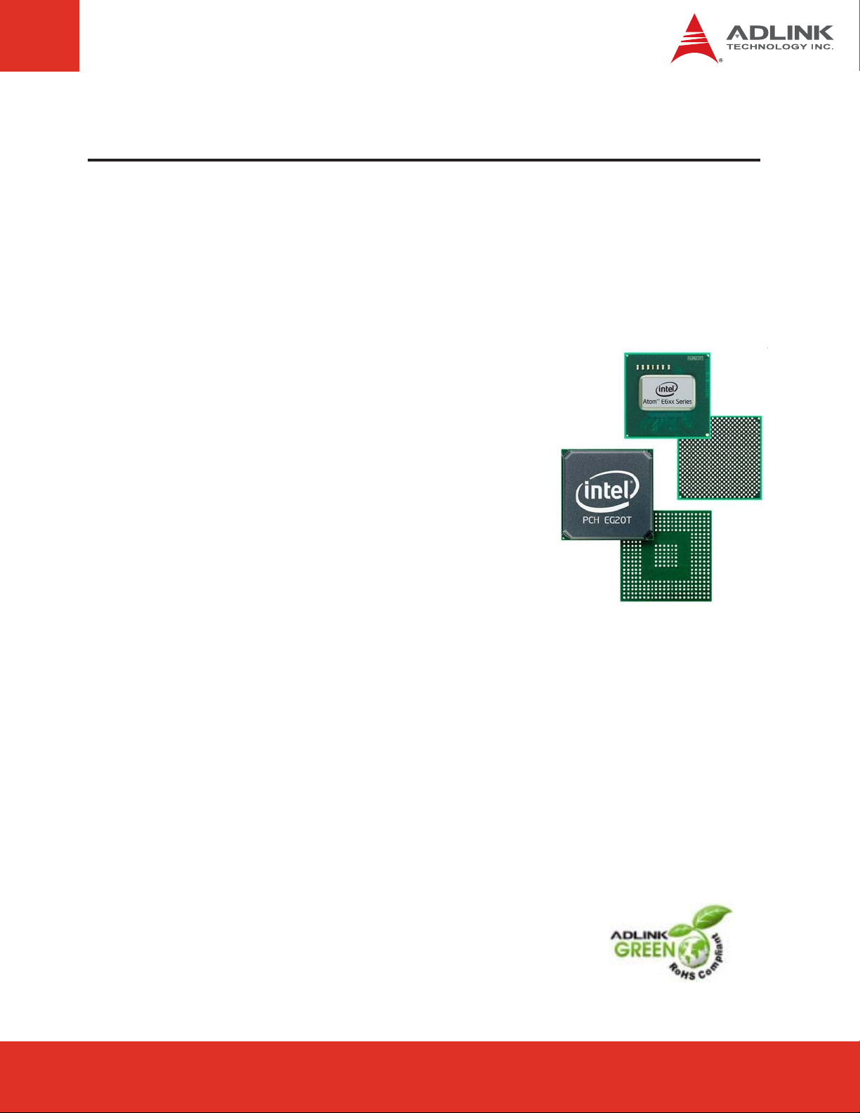
The nanoX-TC is based on the Intel® Atom™ Processor
E6xx with less than 3.9 W thermal design power (TDP).
These new 45nm Intel architecture processors implement
ground-breaking power management techniques, making
them ideal for thermally constrained and fanless embedded
applications. The Processor E6xx series offers an
integrated 2D/3D graphics engine with hardware encode/
decode, LVDS and SDVO output, HD Audio, PCI Express,
and support for Intel® Hyper-Threading and Intel®
Virtualization Technology.
The Intel® EG20T Platform Controller Hub (PCH) provides
additional I/O flexibility with SATA, UART, CAN bus, Gigabit
Ethernet and USB host/client support.
The nanoX-TC allows for innovative designs in mobile and "light" computing, including
portable and mobile equipment for the automotive and test and measurement industries,
visual communication and in the medical field. Using the Intel® Atom™ Processor E6xx and
Intel® EG20T PCH chipset, the nanoX-TC allows developers to utilize a wide variety of
mainstream software applications and middleware familiar to end users that will run
unmodified with full functionality on this platform.
Page 7 Express-IA533 User’s Manual Page 7 Express-IA533 User’s Manual nanoX-TC User’s Manual Page 7
Page 8

2 Specifications
2.1 Core system
CPU
- Intel® Atom™ E680, 1.6 GHz, 3.9 W TDP
- Intel® Atom™ E660, 1.3 GHz, 3.3 W TDP
- Intel® Atom™ E640, 1.0 GHz, 3.3 W TDP
- Intel® Atom™ E620, 600 MHz, 2.7 W TDP
All processors support Intel® Hyper-Threading and Intel® Virtualization Technology
L2 Cache: 512 KB on all processors
Memory: Soldered 512 MB or 1 GB unbuffered DDR2 at 800 MHz
BIOS: AMI UEFI BIOS
Hardware Monitor: Supply voltages and CPU temperature
Debug Interface: XDP SFF-26 extension for ICE debug
Embedded Features: Instant on with Intel Bootloader support, OEM BIOS settings,
Board Info & Statistics, ACPI 3.0, Smart Battery Management support, Watchdog with
programmable timer ranges.
Expansion Busses to carrier board:
- 4 PCI Express x1 (0/1/2/3, port 0 is optionally used for EG20T PCH;
- LPC Bus, SMBus (system) , I2C (user)
- 4 GPI and 4 GPO (shared with SDIO on optional EG20T)
- SPI (supports BIOS only)
2.2 Video
2D/3D Graphics Engine: Integrated in Intel® Atom™ E6xx Processor
Decoding MPEG2, MPEG4, VC1, WMV9, H.264 and DivX
Encoding MPEG4, H.264 (baseline at L3)
no PCIe x4 support)
nanoX-TC User’s Manual Page 8
Page 9

LVDS Interface: Single channel 18- or 24-bit pixel color depths with maximum
resolution of up to 1280x768 @ 60 Hz. Pixel clock rate
between 19.75 MHz (minimum) and 80 MHz (maximum)
SDVO: Serial digital video output supporting devices for DVI, TV-out, analog VGA.
Maximum resolution of up to 1280x1024 @ 85 Hz and pixel clock rate up to 160 MHz.
2.3 Audio
Chipset: Integrated in Intel® Atom™ Processor E6xx
Type: Multi-channel audio stream, 32-bit sample depth, sample rate up to 192 kHz
2.4 LAN
GbE MAC: Integrated in Intel® EG20T PCH
PHY: Realtek RTL8211CL
Speed: 10/100/1000 Mbps
2.5 Multi I/O
Chipset: Integrated in Intel® PCH EG20T
USB: Six USB 1.1/2.0 host ports and one USB 1.1/2.0 client port
SATA: Two ports supporting SATA 1.5 Gb/s and 3 Gb/s
SDIO Port: SDIO/MMC supporting SDHC speed class 6 (shared with GPIO)
SDIO Storage: TBD
Serial and CAN: One RS-232 (RX/TX) and one CAN (AX/RX) port (optional 2x RS-232
w/o CAN)
2.6 Super I/O
Connected to LPC bus on carrier if needed (standard support for Winbond W83627DHG)
Page 9 Express-IA533 User’s Manual Page 9 Express-IA533 User’s Manual nanoX-TC User’s Manual Page 9
Page 10

2.7 SDIO/MMC Extension
Chipset: Integrated in Intel® Controller Hub
Type: Single port SDIO/MMC supports SDIO specification 1.1 and MMC specification 4.0
Connection: Multiplexed over GPIO signals to carrier
2.8 Operating Systems
Standard Support
- Windows 7
- Linux 2.6.x
Extended Support (BSP)
- Linux BSP
- AIDI I2C Library for Windows and Linux
- WinCE 6.0 / 7.0
- Windows XP Embedded
2.9 Mechanical and Environmental
Standard Operating Temperature: 0°C to 60°C
Relative Humidity: up to 90% at 55°C
Form Factor and Type: PICMG COM.0, COM Express™ Type 10 compatible
Dimensions: 85 x 55 mm
2.10 Power Specifications
Input Power: 4.75 V – 21 V wide range, supports AT mode and ATX mode
(with additional 5 Vsb)
Power States: Supports S0, S3, S4, S5
Power Consumption: 6W at 5V typical, 5W idle
Smart Battery Support: Yes
nanoX-TC User’s Manual Page 10
Page 11

2.11 Power Consumption
nanoX-TC-E62 0 (2G ) 4.5 5.5 N/A 1.3 0.4
nanoX-TC-E64 0 (2G ) 4.7 6.3 N/A 1.4 0.4
nanoX-TC-E66 0 (2G ) 5.0 6.6 N/A 1.4 0.4
nanoX-TC-E68 0 (2G ) 5.2 7.4 N/A 1.3 0.4
2.12 Ordering Codes
nanoX-TC-E680-1G: Mini size COM Express Type 10 Module with Intel® Atom™ E680
processor at 1.6GHz, PCH EG20T and 1 GB DDR2 SDRAM
Power Consumption [W]
12V 12V 12V 5Vsb 5Vsb
Idle
WinXP Login
Max Load
WinXP
Burnin/Kpower
S1
Standby
Powered On
S3
Suspend to RAM
S5
Soft Off
nanoX-TC-E660-1G: Mini size COM Express Type 10 Module with Intel® Atom™ E660
processor at 1.3GHz, PCH EG20T, and 1 GB DDR2 SDRAM
nanoX-TC-E640-1G: Mini size COM Express Type 10 Module with Intel® Atom™ E640
processor at 1.1GHz, PCH EG20T, and 1 GB DDR2 SDRAM
nanoX-TC-E620-1G: Mini size COM Express Type 10 Module with Intel® Atom™ E620
processor at 600 MHz, PCH EG20T, and 1 GB DDR2 SDRAM
Page 11 Express-IA533 User’ s Manual Page 11 Express-IA533 User’ s Manual nanoX-TC User’s Manual Page 11
Page 12
3 Functional Diagram
BIOS
SPI
LPC bus
512 MB ~ 2 GB DDR2
Soldered Memory
AB
18/24-bit LVDS
SDVO
HDA Audio
3x PCIe x1 (port 1~3)
PCIe x1 (port 0)
CAN Bus (Ax/Rx)
UART (Tx/Rx)
2x SATA (port 0,1)
6x USB Host
1x USB Client
LAN PHY
RTL8211CL
Intel® Atom™
processor
E6xx
PCIe x1 (port 0)
Intel®
Platform
Controller
Hub
EG20
SDIO/MMC port 0
4x GPI
4x GP0
Switch
GPIO
PCA9535
I2C
SMBus
BC
nanoX-TC User’s Manual Page 12
Page 13
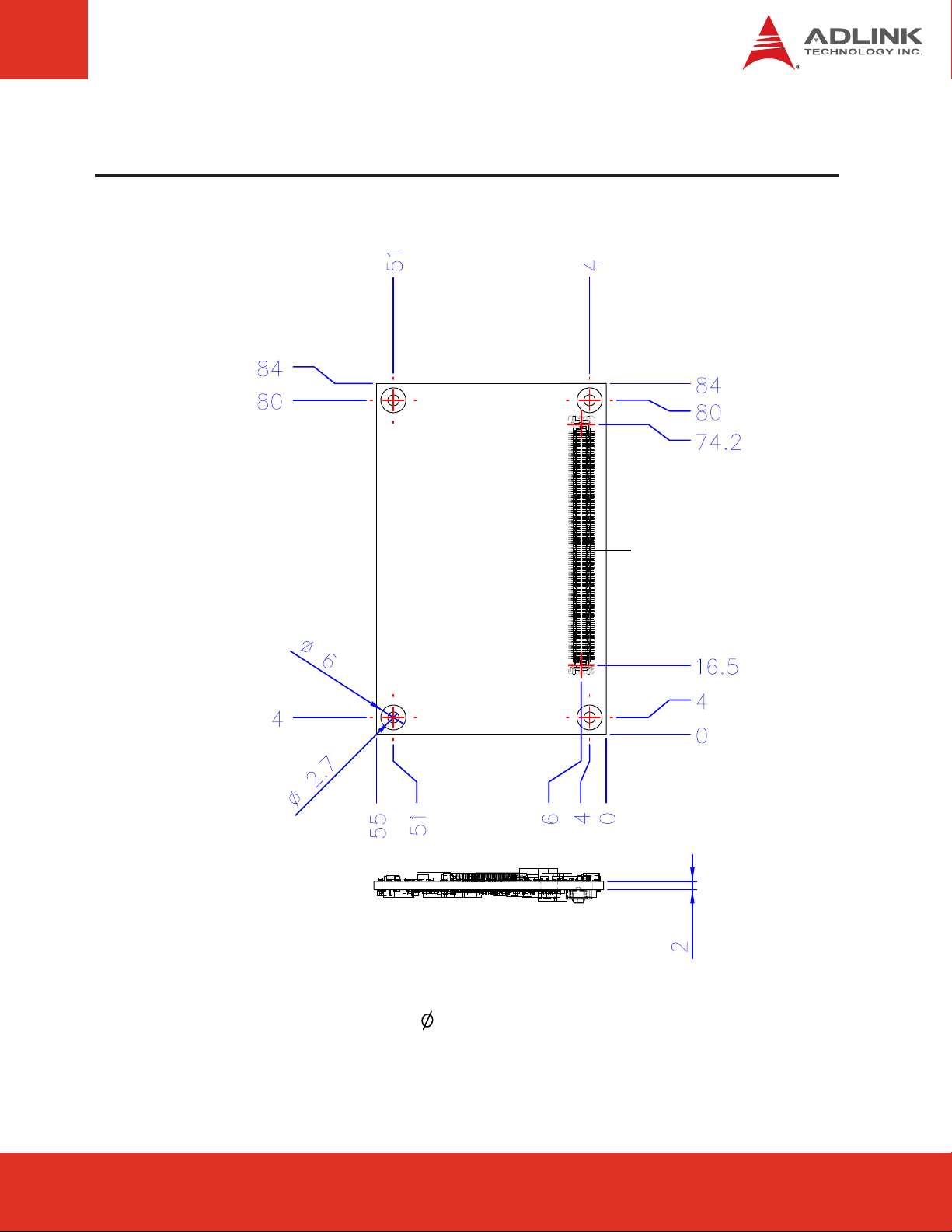
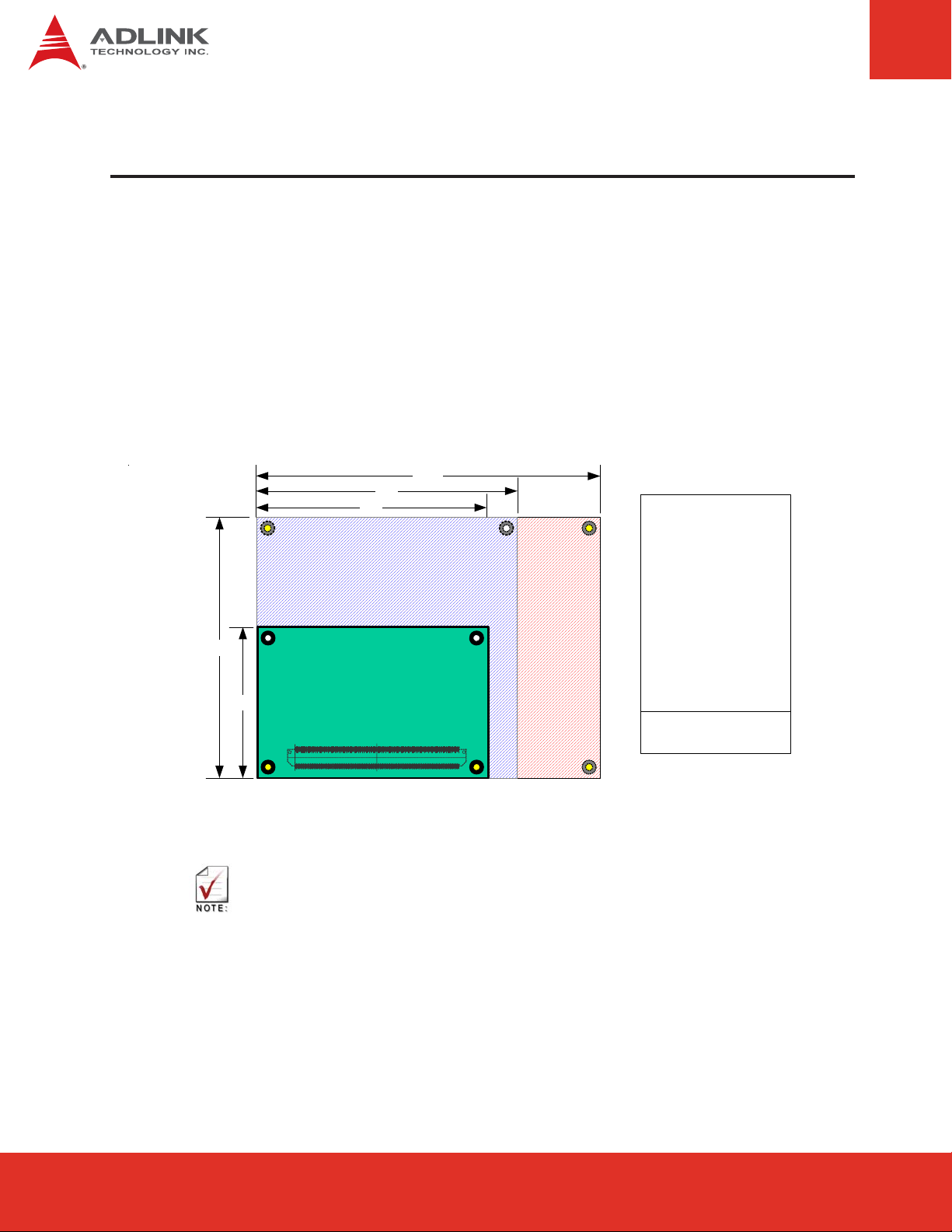
4 Mechanical Dimensions
Top View
Side View
connector on
bottom side
All tolerances ± 0.05 mm
Other tolerances ± 0.2 mm
Page 13 Express-IA533 User’ s Manual Page 13 Express-IA533 User’ s Manual nanoX-TC User’s Manual Page 13
Page 14
5 Pinout and Signal Descriptions
5.1 COM Express™ Type 10 Pinout
All pinouts on AB connector of the nanoX-TC comply with pin-out and signal descriptions
®
used in the “PICMG
This chapter details pinouts, signal descriptions, and mechanical characteristics of the
nanoX-TC.
An additional document, the “PICMG COM Express Design Guide” gives a general
introduction to carrier board designs for COM Express
95
55
COM.0 R2.0: COM Express® Module Base Specification Type 2”.
™
modules.
.125.
.95.
.84.
- AC'97 or High Definition Audio
- Dual 24-b it LVDS channels
- Primary power input: +12V,
- Gigabit Ethernet port
- LPC interface
- 4 Serial ATA channels
- 6 USB 2.0 ports
- 6 PCI Express x1 Lanes
- SDVO
- GPIO / SDIO
- Keyboard
2
- I
C / SMBus
-SPI support
+5V standby and 3.3V RTC
AB
AB Connector
Dimensions in mm
The above function mappings are a generic description of COM Express pinouts,
and not necessarily supported on the module described in this manual.
nanoX-TC User’s Manual Page 14
Page 15
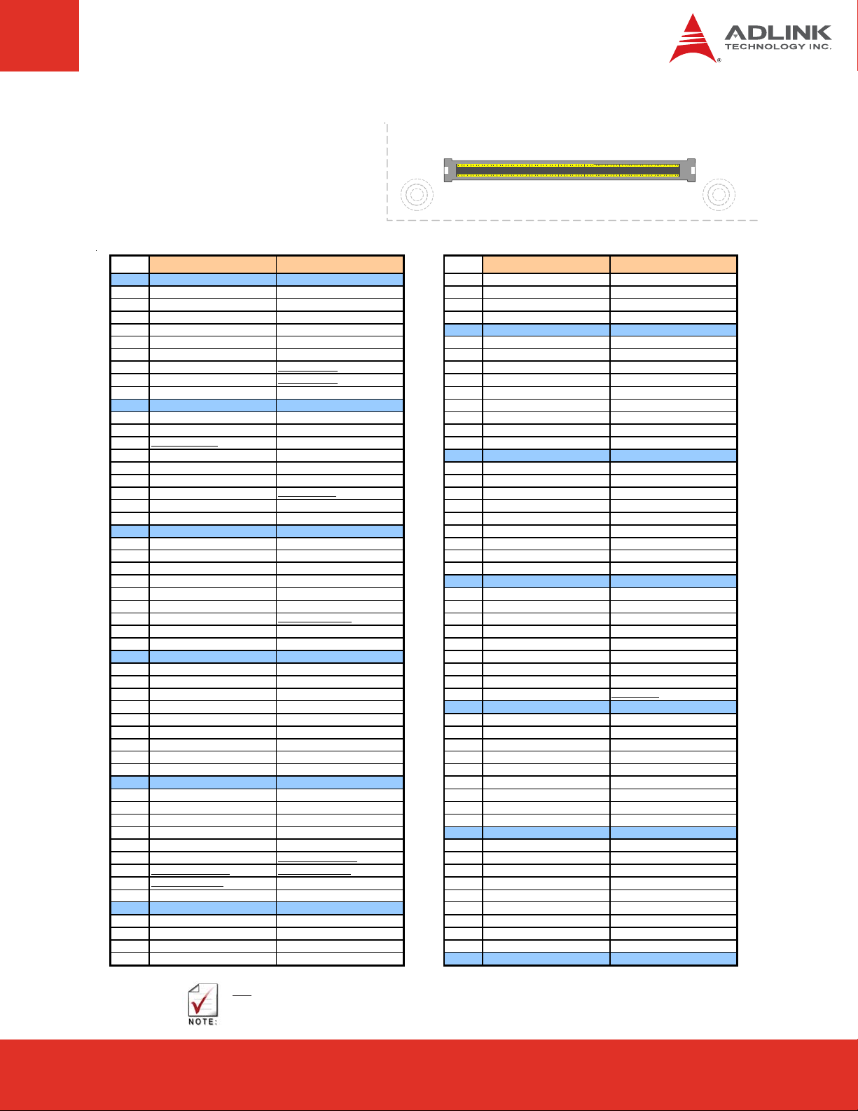
5.2 Pin Definitions
(
)
)
B1
Pinouts comply with
COM Express Type 10
Pin Row A Row B Pin Row A Row B
1 GND(FIXE D) GND(FIXED) 56 RSVD RSVD
2 GBE 0_MDI3- GBE0_ACT# 57 G ND GPO2
3 GBE0_MDI3+ LPC_FRAME# 58 PCIE_TX3+ PCIE_RX3+
4 GB E0_ LINK100# LP C_ AD0 59 P C IE _TX3- P CIE _R X 35 GB E 0_ LINK1000# LP C_ AD1 60 G ND(F IXE D) G ND(F IXE D)
6 GB E 0_ MDI2- L PC _ AD2 61 PC IE _ T X2+ P C IE _ R X 2+
7 GB E 0_ MDI2+ L PC _ AD3 62 P C IE_ TX 2- PCIE _RX 28 GB E 0_ LINK# L P C_ DRQ0#
9 GB E 0_ MDI1- LP C_ DR Q1#
10 GBE0_MDI1+ LPC_CLK 65 PCIE_TX1- PCIE_RX111 GND(F IX E D) G ND(F IXE D) 66 G ND WAK E 0#
12 GBE0_MDI0- PWRBTN# 67 GPI2 WAKE1#
13 GBE0_MDI0+ SMB_CK 68 PCIE_TX0+ PCIE_RX0+
14 GBE0_CTREF
15 S U S _ S3# S MB_ ALE RT# 70 G ND(F IXE D) GND(FIX E D)
16 SATA0_TX + S ATA1_TX+ 71 LVDS _A0+ DDI0_PAIR0+
17 SATA0_TX - SATA1_TX- 72 LVDS _A0- DDI0_PAIR018 SUS_ S 4# SUS_ STAT#
19 SATA0_RX+ S ATA1_R X+ 74 LVDS_ A1- DDI0_PAIR120 SATA0_RX- S ATA1_R X- 75 LVDS _A2+ DDI0_PAIR2+
21 GND(F IX E D) G ND(F IXE D) 76 L V DS _A2 - DDI0 _ P AIR 222 RSVD RSVD 77 LVDS_ VDD_E N DDI0_PAIR4+
23 RS VD R S VD 78 LVDS_A3+ DDI0_PAIR424 SUS_S5# PWR_OK 79 LVDS_A3- LVDS_BKLT_EN
25 RS VD R SVD 80 G ND(F IXE D) G ND(FIX E D)
26 RSVD RSVD 81 LVDS_A_CK+ DDI0_PAIR3+
27 BATLO W# W DT 82 L V DS _A_ CK- DDI0 _ P A IR 3 28 (S)ATA_ACT# AC/HDA_SDIN2
29 AC/HDA_S Y NC AC/HDA_ SDIN1 84 LVDS_I2C_DAT VCC _ 5V_SB Y
30 AC/HDA_RST# AC/HDA_ S DIN0 85 GPI3 VCC_5V_SBY
31 GND(F IX E D) G ND(F IXE D) 86 R SVD V C C _5V _ SB Y
32 AC/HDA_BITCLK SPKR 87 RSVD VCC_5V_SBY
33 AC /HDA_ S DOUT I2C_ C K 88 P C IE _CLK _ RE F+ BIOS _DIS 1#
34 BIOS_DIS0# I2C_DAT 89 PCIE_ CLK_ REF- DD0_HPD
35 THRMTR IP # T HR M# 90 G ND(F IXE D) G ND(FIX E D)
36 USB6- USB7- 91 S P I_P OWER DDI0_PAIR5+
37 USB6+ USB7+ 92 SPI_MISO DDI0_PAIR538 USB_6_7_OC# USB_4_5_OC# 93 GPO0 DDI0_PAIR6+
39 USB4- USB5- 94 S P I_C LK DDI0_PAIR640 USB4+ US B5+ 95 SPI_MOSI DDI0_DDC_ AUX_S E L
41 GND(F IX E D) G ND(F IXE D) 96 T P M_ PP R S VD
42 USB2- USB3- 97 TYPE10# S PI_CS#
43 USB2+ US B3+ 98 SE R0_TX DDI0_CTRLCLK_ AUX+
44 USB_2_3_OC# USB_0_1_OC# 99 SER0_RX DDI0_CTRLDATA_AUX45 USB0- USB1- 100 GND(FIXED) GND(FIXED)
46 USB0+ US B1+ 101 SE R1_ TX FAN_ PWMOUT
47 VCC_R TC E XCD1_PERST#
48 EXCD0_PE RS T#
49 EXCD0_CPPE #
50 LPC_S ERIRQ CB_RESE T# 105 VCC_12V VCC_12V
51 GND(F IX E D) G ND(F IXE D) 106 VC C _ 12V V CC_ 12V
52 RSVD RSVD 107 VCC_12V VCC_12V
53 RSVD RSVD 108 VCC_12V VCC_12V
54 GPI0 GPO1 109 VCC_12V VCC_12V
55 RSVD RSVD 110 GND
SMB_DAT 69 PCIE_TX0- PCIE_RX0-
EXCD1_CPPE# 103 LID# S LE E P#
SYS_RESET# 104 VCC_12V VCC_12V
A1
63 GPI1 GPO3
64 PCIE_ TX1+ P CIE_RX 1+
73 LVDS _A1+ DDI0_PAIR1+
83 LVDS_I2C_CK LVDS_BKLT_CTRL
102 SE R1_RX FAN_TACHIN
FIXED
GND(FIXED
B110
A110
A B
XXX Strikethrough pin names indicates that the signal is not supported on this module.
Page 15 Express-IA533 User’ s Manual Page 15 Express-IA533 User’ s Manual nanoX-TC User’s Manual Page 15
Page 16
5.3 Signal Descriptions
p
_
_
p
p
#
p
_
(
)
p
p
#
_
_S4#
y
g
_S5#
y
#
y
#
(
)
_
_6_7_OC#
#
y p
#
Pin Signal Des c ription TypePU/PD Comment
A1 G ND(F IX E D) Ground P WR - A2 GBE0_MDI3- Ethernet Media De
A3 GBE 0
A4 GBE 0
A5 G BE 0 _ L INK 1000# E thernet 1000 Mbit/se c Link Indicator OD - On at 1000Mb/s
A6 GBE0_MDI2- Ethernet Media De
A7 GBE0_MDI2+ Ethernet Media De
A8 G BE 0_LINK
A9 GBE0_MDI1- Ethernet Media De
A10 GBE 0
A11 G ND
A12 GBE 0_MDI0- E thernet Media De
A1 3 G BE 0_ MDI0 + E the r ne t Med i a De
A14 G BE 0_CTR E F
A15 S US_S 3
A16 S ATA0_ T X + S AT A 0 T ransmit Data + O - DP - A17 SATA0
A18 S US
A19 S ATA0 _ R X + S ATA 0 Re ceive Data + I - DP - A20 SATA0_R X - S ATA 0 Rece ive Data - I - DP - A21 G ND(F IX E D) Ground P WR - A22 RS VD Clock s
A23 RS VD NC - A24 S US
A25 RS VD NC - A26 RS VD NC - A27 B AT LOW# Batter
A28 (S )ATA_ ACT
A29 AC /HDA_ SYNC HDA S
A30 AC/HDA_ R S T
A31 G ND
A32 AC/HDA
A33 AC/HDA_ S DOUT HD A Data O-3.3 - A34 BIOS _ DIS0# L P C BIOS boot device selection I-3.3 PU 10k 3.3V A35 THR MT R IP # C P U Thermal shudown inidcator O-3.3 P U 1k 3.3V A36 US B6- US B Data - Port6 I/O - DP - A37 US B6+ US B Data + Port6 I/O - DP - A38 US B
A39 US B4- US B Data - Port4 I/O - DP - A40 US B4+ US B Data + Port4 I/O - DP - A41 G ND(F IX E D) Ground P WR - A42 US B2- US B Data - Port2 I/O - DP - A43 US B2+ US B Data + Port2 I/O - DP - A44 USB_2_3_OC
A45 US B0- US B Data - Port0 I/O - DP - A46 US B0+ US B Data + Port0 I/O - DP - A47 VCC_RTC E xternal RTC batter
A48 E XCD0_ PE RS T
A49 E XCD0_C P PE #
A50 LPC_SERIRQ LPC INT_SERIRQ | Serial Interrupt Request IO-3.3 PU 10k 3.3V A51 G ND(F IX E D) Ground P WR - A52 RS VD NC - A53 RS VD NC - A54 G P I0 G P I0 or SD IO c ontroller 0 data 0 IO-3.3 P U 10k 3.3V B IO S select
A55 RS VD NC - -
MD I3 + E th e rne t Me d ia Dependent Interface + I/O - DP - -
LINK100#E thernet 100 Mbit/s ec L ink Indicator OD - On at 100Mb/s
E thernet Llink Indicator (all speeds) O-3.3 - -
MD I1 + E th e rne t Me d ia Dependent Interface + I/O - DP - -
FIXED
TX - S AT A 0 T ransmit Data - O - DP - -
FIXED
BITCLK HDA Clock O-3.3 - -
Ground PWR - -
E thernet center tap re fe re nc e vol tage NC - not supported
S3 Suspend to RAM inidcator O-3.3 - -
S4 Hibernation inidcator O-3.3 - -
S 5 S oft Off inidcator O-3.3 - -
S ATA L E D O-3. 3 P U 10k 3. 3V -
HDA R eset O-3.3 - Ground PWR - -
US B OverC urrent Port 6/7 I -3.3 P U 10k 3. 3Vs b -
US B OverC urrent Port 2/3 I -3.3 P U 10k 3. 3Vs b -
Express Ca rd Support [0] | card reset O-3.3 P U 10k 3.3V not supported
Express Ca rd Support [0] | cap. card req. I-3.3 P U 10k 3. 3V not supported
Row A
endent Interface - I/O - DP - -
endent Interface - I/O - DP - endent Interface + I/O - DP - -
endent Interface - I/O - DP - -
endent Interface - I/O - DP - endent Interface + I/O - DP - -
nc signal to Dialo
Low Input I-3.3 - -
nc O-3.3 - -
owe r P W R - -
CLK IN - -
XXX Strikethrough pin names indicates that the signal is not supported on this module.
nanoX-TC User’s Manual Page 16
Page 17
Signal Descriptions (cont’d)
_
)
p
_
)
p
_
_
p
#
p
Row A
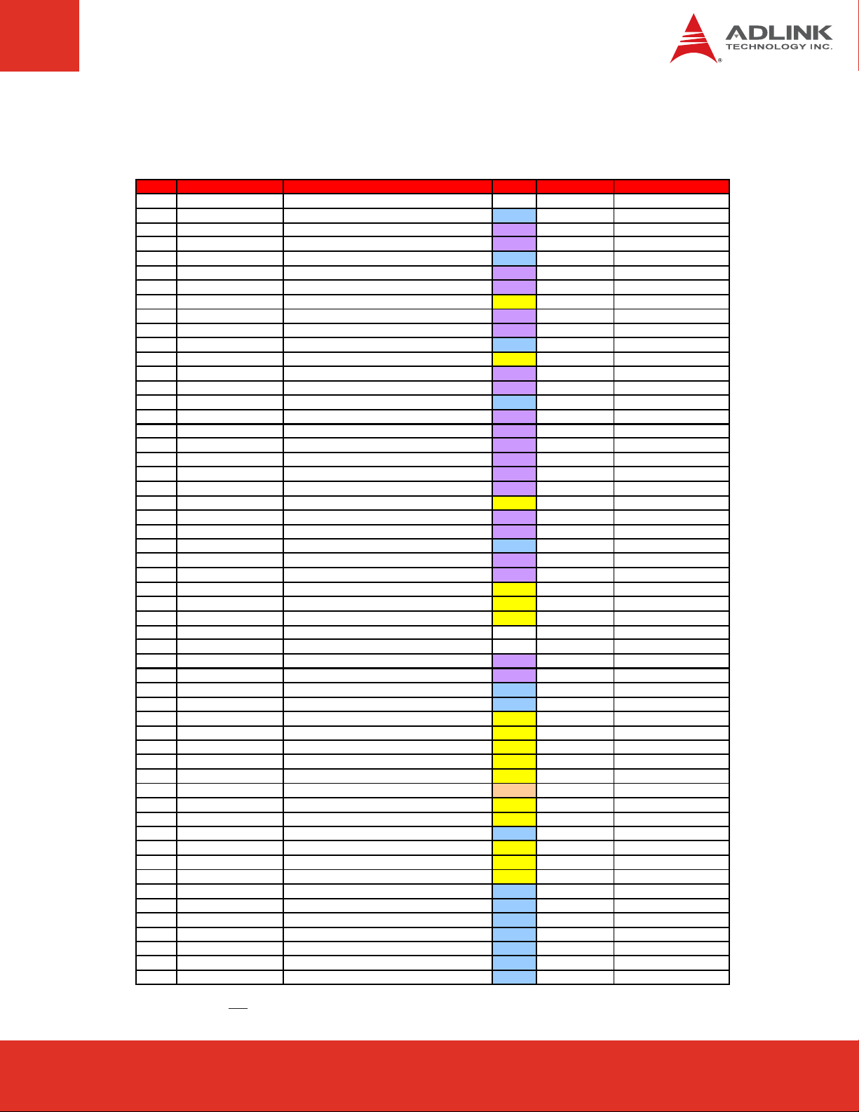
Pin Signal Des c ription TypePU/PD Comment
A56 RS VD NC - A57 G ND Ground P WR - A58 P C IE _ T X3+ P C Ie 3 TX + (port 0 of CP U, occupied) O - DP - use d for PC H E G20T
A59 P CIE
A60 G ND(F IX E D) Ground P WR - A61 P C IE _ TX2+ PC Ie 2 TX+ (
A62 P C IE _ TX2- P C Ie 2 TX- (port 3 of CP U) O - DP - A63 G P I1 GP I1 or S DIO controller 0 data 1 IO-3.3 P U 10k 3.3V B IOS sele ct
A64 P C IE _ TX1+ PC Ie 1 TX+ (port 2 of CP U) O - DP - A65 P CIE
A66 G ND Ground P WR - A67 G P I2 GP I2 or S DIO controller 0 data 2 IO-3.3 P U 10k 3.3V B IOS sele ct
A68 P C IE _ TX0+ PC Ie 0 TX+ (port 1 of CP U) O - DP - A69 P C IE _ TX0- P C Ie 0 TX- (
A70 G ND(F IX E D) Ground P WR - A71 L VDS _ A0+ L VDS Channel A O - DP - A72 L VDS_ A0 - LVDS Channel A O - DP - A73 L VDS
A74 L VDS_ A1 - LVDS Channel A O - DP - A75 L VDS _ A2+ L VDS Channel A O - DP - A76 L VDS_ A2 - LVDS Channel A O - DP - A77 LV DS _ VDD_ E N L VDS VDD P anel Power O-2,5 P D 10k A78 L VDS _ A3+ L VDS Channel A O - DP - A79 L VDS
A80 G ND(F IX E D) Ground P WR - A81 LVDS _A_ C K+ LVDS C hannel A Clock O - DP - A82 LVDS _A_ C K - L VDS Channel A Clock O - DP - A83 LVDS _ I2C _ C K L VDS I2C C lock IO-3.3 PU 2 .2 k 3.3V A84 LVDS_I2C _ DAT L VDS I2C Data IO-3.3 PU 2.2k 3.3V A85 G P I3 GP I3 or S DIO controller 0 data 3 IO-3.3 P U 10k 3.3V B IOS sele ct
A86 RS VD NC - A87 RS VD NC - A88 PCIE_ CLK_REF+ PCI Express Clock Reference O - DP - A89 PCIE_CLK_REF- PCI Ex
A90 G ND(F IX E D) Ground P WR - A91 S P I_ POWE R P ower source for SPI devices on carrier PWR - A92 S PI _ MIS O D a ta in to Module from C arrie r S P I I -3. 3 A93 GP O0 G P O0 or SDIO controller 0 clock O-3.3 P U 10k 3.3V B IOS sele ct
A94 SPI_CLK Clock from Module to Carrier SPI O-3.3 A95 S PI_MOSI Data out from Module to Carrier SPI O-3.3 A96 TPM_PP (TPM) Physical Presence pin I-3.3 A97 TY P E10
A98 S E R0_ TX S erial 0 port transmitter O-5 -
A99 S ER 0_R X S erial 0
A100 G ND(F IXE D) Ground P WR - A101 S E R1_ T X S erial 1 port trans mitter / or CAN CAN_ AX O-5 A102 S ER 1_ R X S erial 1 port receiver / or CA N CAN_ R X I-5 A103 L ID # ACPI type LID switch I-3.3 P U 4 .7 k 3.3V
A104 VC C _ 12V P ower 12V P WR - A105 VC C _ 12V P ower 12V P WR - A106 VC C _ 12V P ower 12V P WR - A107 VC C _ 12V P ower 12V P WR - A108 VC C _ 12V P ower 12V P WR - A109 VC C _ 12V P ower 12V P WR - A110 G ND(F IXE D) Ground P WR - -
T X3- PC Ie 3 TX- (port 0 of CP U, occupied
ort 3 of C P U) O - D P - -
T X1- PC Ie 1 TX- (port 2 of CP U
ort 1 of CP U ) O - DP - -
A1+ LVDS Channel A O - DP - -
A3- LVDS Channel A O - DP - -
ress Clock Reference O - DP - -
Rev 2.0 / Type 10 indicator to carrier ST O P D 4.7k -
ort rec eive r I -5 -
O - DP - used for PC H E G 20T
O - DP - -
XXX Strikethrough pin names indicates that the signal is not supported on this module.
Page 17 Express-IA533 User’ s Manual Page 17 Express-IA533 User’ s Manual nanoX-TC User’s Manual Page 17
Page 18
Signal Descriptions (cont’d)
#
_
_
p
p
p
Q0#
Q1#
_
(
)
#
#
_
_
_
(
)
p
y
g
_
p
p
p
purp
_
#
p
p
#
(
)
#
#
_
_
Row B
Pin Signal Desc ription Type PU/PD C omment
B 1 GND(F IXE D) Ground PWR - B2 GBE0_ACT
B3 LPC
B4 LPC
B5 LPC_AD1 LPC multi
B6 LPC_AD2 LPC multi
B7 LPC_AD3 LPC multi
B8 LPC_DR
B9 LPC_DR
B10 LPC
B11 GND
B12 PWRBTN
B 1 3 S MB _ C K S MB us C lock I O-3.3 P U 2k 2 3 . 3 V s b B14 S MB_DAT S MBus Data IO-3.3 PU 2k2 3.3Vsb B15 SMB_ALERT
B16 SATA1_TX + S ATA 1 Transmit Data + O - DP - B17 SATA1
B18 SUS
B19 SAT A1_ R X+ S ATA 1 Receive Da ta + I - DP - B20 SATA1
B21 GND
B22 RSVD
B23 RSVD
B24 PWR_OK Power OK from main
B25 RSVD
B26 RSVD
B27 WDT Watch Do
B28 AC/HDA
B29 AC /HDA_ S DIN1 S erial T DM data in
B30 AC /HDA_ S DIN0 S erial T DM data in
B31 GND(FIXED) Ground PWR - B32 SPKR Out
B33 I2C_CK General
B34 I2C
B35 THRM
B 36 US B 7- US B Da ta - P ort7 I /O - DP - clie nt
B37 US B7+ US B Data + Port7 I/O - DP - client
B38 USB_4_5_OC
B 39 US B 5- US B D a ta - P or t5 I/O - DP - B40 US B5+ US B Data+ Port5 I/O - DP - B41 GND
B 42 US B 3- US B D a ta - P or t3 I/O - DP - B43 US B3+ US B Data+ Port3 I/O - DP - B44 USB_0_1_OC
B 45 US B 1- US B D a ta - P or t1 I/O - DP - B46 US B1+ US B Data+ Port1 I/O - DP - B47 EXCD1_PE RST
B48 E XCD1
B49 SYS
B50 CB_ RE S ET# Reset output from Module to Carrier Board O-3.3 - B51 GND(FIXED) Ground PWR - B52 RSVD NC - B53 RSVD NC - B54 GPO1 GP O1 or SDIO contr. 0 Command/R esponse IO-3.3 PU 10k 3.3V BIOS select
B55 RSVD NC - -
FRAME# LPC Frame Indicator O-3.3 - -
AD0 LP C multiplexed Adress & DATA B us IO-3.3 - -
CLK LPC Clock O-3.3 - -
FIXED
TX - S AT A 1 T ransmit Data - O - DP - -
STAT# I mmine nt suspend operation inidcator O-3.3 - not supported
RX - S AT A 1 Receive Data - I - DP - -
FIXED
SDIN2 Serial TDM data input 2 I-3.3 - not s upported
DAT General purpos e I2C port data I/O line IO-3.3 PU 4k7 3.3V
FIXED
CPPE# PCI Express capa ble ca rd reque st O-3.3 - not supported
RESET# Reset Button Input I-3.3 none 3.3Vsb
Ethernet Activity LED OD - -
lexed Adress & DATA B us IO-3.3 - lexed Adress & DATA B us IO-3.3 - -
lexed Adress & DATA B us IO-3.3 - LPC Serial DMA Request 0 I-3. 3 - not s upported
LPC Serial DMA Request 1 I-3. 3 - not s upported
Ground PWR - P ower Button I-3.3 P U 10K 3.3Vs b -
System Management Bus Alert for S MI I-3.3 PU 10k 3.3V
Ground PWR - -
NC
ower s uppl
E ve nt occurred indicator O-3.3 PU 10K 3.3Vs b
ut 1 I-3. 3 - ut 0 I-3. 3 - -
ut for audio enun ciator (P C Beep)O-3.3- -
os e I2C port c loc k output IO-3.3 PU 4k7 3.3V
Off module over temperature indicator I-3.3 PU 1k2 3.3V -
USB OverC urrent Port 4,5 I-3.3 PU 10k 3.3Vsb -
Ground I-3.3 - -
USB OverC urrent Port 0,1 I-3.3 PU 10k 3.3Vsb -
PCI Express Card Reset signa l O-3.3 - not supported
NC
I-3.3 - always reserve pull up
NC
NC
--
--
--
--
ort
ort
XXX Strikethrough pin names indicates that the signal is not supported on this module.
nanoX-TC User’s Manual Page 18
Page 19
Signal Descriptions (cont’d)
t
_
)
p
_
)
#
#
p
+
_
_
p
y
_5V_
t
_
#
Row B
Pin Signal Desc ription TypePU/PD Comment
B56 RSVD NC - B57 G P O2 GP O2 or S DIO controller 0 Write Protec
B58 P CIE _R X3+ P C Ie 3 R X+ (port 0 of CP U, occupied) I - DP - used for PCH E G20T
B59 PCIE
B60 GND(FIXED) Ground PWR - B61 P CIE _ RX 2+ P C Ie 2 RX+ (
B62 P C IE_ RX 2- P C Ie 2 R X- (port 3 of CP U) I - DP - B63 G P O3 GP O3 or S DIO controller 0 Card Detect IO-3.3 PU 10k 3.3V B IOS select
B64 P CIE _ RX 1+ P C Ie 1 RX+ (port 2 of CP U) I - DP - remove L AN to us e
B65 PCIE
B66 WAKE 0# P C I Expres s wak e up signal. I-3. 3 none 3.3 Vs b conne cted to WAKE 1
B67 WAKE1# General Purpos e wa ke up signal I-3. 3 none 3.3 Vsb conne cted to WAKE 0
B68 P CIE _R X0+ P C Ie 0 R X + (port 1 of CP U) I - DP B69 PCIE_RX0- PCIe 0 RX- (
B70 GND(FIXED) Ground PWR - B71 DDI0_PAIR0+ S DVOB_RED
B72 DDI0_PAIR0- SDVOB_RED- O - DP - B73 DDI0
B74 DDI0_PAIR1- SDVOB_GRN- O - DP - B75 DDI0_PAIR2+ S DVOB_BLU+ O - DP - B76 DDI0_PAIR2- SDVOB_BLU- O - DP - B77 DDI0_PAIR4+ S DVOB_INT+ I - DP - B78 DDI0_ PAIR4- S DVOB_ INT- I - DP - B79 LVDS
B80 GND(FIXED) Ground PWR - B81 DDI0_PAIR3+ S DVOB_CK+ O - DP - B82 DDI0_PAIR3- SDVOB_CK O - DP - B83 LVDS_BKLT_CTRL LVDS
B84 VCC_5V_SBY 5V Standby Input PWR - B85 VCC_5V_SBY 5V Standb
B86 VCC_5V_SBY 5V Standby Input PWR - B87 VCC
B88 BIOS_DIS 1# SPI BIOS boot device selection I-3.3 PU 10k 3.3Vsb B89 DD0_HPD
B90 GND(FIXED) Ground PWR - B91 DDI0_PAIR 5+ SDVO_ TVCLKIN+ I - DP - B92 DDI0_ PAIR5- S DVO_TVCL KIN- I - DP - B93 DDI0
B94 DDI0_PAIR6- SDVO_FLDSTALL- I - DP - B95
DDI0_DDC_AUX_SEL
B96 RSVD NC - B97 S PI_CS
B98
DDI0_C TR LCLK _AUX+
DDI0_CTR LDATA_AUX-
B99
B100 GND(FIXE D) Ground P WR - B1 01 F AN_P WMOUT F a n s peed control output O-3.3 P U 1.2K 3.3Vs b
B102 FAN_T ACHIN F a n tachometer input I-3.3 P D 10k B1 03 S L EE P# s leep I-3.3 - B1 04 VC C _ 12V P ower 12V PWR - B1 05 VC C _ 12V P ower 12V PWR - B1 06 VC C _ 12V P ower 12V PWR - B1 07 VC C _ 12V P ower 12V PWR - B1 08 VC C _ 12V P ower 12V PWR - B1 09 VC C _ 12V P ower 12V PWR - B110 GND(FIXE D) Ground P WR - -
RX3- PCIe 3 RX- (port 0 of CPU, occ upied
ort 3 of C P U) I - DP - -
RX1- PCIe 1 RX- (port 2 of CP U
ort 1 of CPU) I - DP -
PAIR1+ SDVOB_GRN+ O - DP - -
BKLT_EN LVDS panel backlight enable O-3.3 PD 100k -
anel backlight brightness control O-3.3 PD 10k -
Input PWR - -
SBY 5V Standby Input PWR - -
Digita l D i splay Inte rfac e Hot-P lug Detec
PAIR6+ SDVO_FL DSTAL L+ I - DP - -
S elec t function of DDI(0) CT R L_ C LK _ AUX+ IO-3.3 - -
Chip se lect for C arrie r B oard S PI O-3. 3 none 3. 3 V s b SDVO I2C Clock IO-2.5
SDVO I2C Data IO-2.5
IO-3.3 PU 10k 3.3V BIOS select
I - DP - used for PCH E G20T
I - DP - remove LAN to us e
O - DP - -
I-3.3 P U 10k 3.3V not needed on SDVO
XXX Strikethrough pin names indicates that the signal is not supported on this module.
Page 19 Express-IA533 User’ s Manual Page 19 Express-IA533 User’ s Manual nanoX-TC User’s Manual Page 19
Page 20

Signal Description Legend
IO-2,5 Bi-directional 2,5 V Input/Output
IO-3,3 Bi-directional 3,3 V Input/Output
IO-5 Bi-directional 5 V Input/Output
I-3,3 3,3 V Input
I- 5 5 V Inp ut
O-2,5 2,5 V Output
O-3,3 3,3 V Output
O-5 5 V Output
IO Input/Output
OA Analog Output
OD Digital Output
I/O - DP Differential Pair Input/Output
O - DP Differential Pair Output
I - DP Differ e n t ia l Pa ir Inpu t
PWR Power or Ground
STO Strapping Ou tpu t
PU Pull Up Resisto r
PD Pull Down Resis t or
NC Not Connected / Reserved
Signal Type Legend
nanoX-TC User’s Manual Page 20
Page 21

6 Embedded Functions
All embedded board functions on ADLINK’s Computer on Modules are supported at the
operating system level using the ADLINK Intelligent Device Interface (AIDI) library. The AIDI API
programming interface is compatible and identical across all ADLINK Computer on Modules
and all supported operating systems. The AIDI library includes a demo program to
demonstrate the library’s functionallity.
6.1 Watchdog Timer
The nanoX-TC implements a watchdog timer that can be used to
automatically detect software execution problems or system hangs
and reset the board if necessary. The watchdog timer consists of a
counter that counts down from an initial value to zero. When the
system is operating normally, the software that sets the intial value
periodically resets the counter so that the it never reaches zero. If
the counter reaches zero before the software resets it, the system
is presumed to be malfunctioning and a reset signal is asserted.
The AIDI Library Watchdog Functions support watchdog control of the board. If the watchdog
begins countdown and reaches zero, it will access the CPU's RESET signal to reset the
system. The watchdog application must call another function named AidiWDogTrigger that
restarts the Watchdog timer in order to prevent system reset.
AIDI Demo Program
- Watchdog Ta b
The AIDI Demo Program allows
retrieval of the current
watchdog status and updating
of the watchdog settings
If the watchdog is enabled, the
user can click the WDT Trigger
button to manually reset the
counter and prevent the system
from resetting
Page 21 Express-IA533 User’ s Manual Page 21 Express-IA533 User’ s Manual nanoX-TC User’s Manual Page 21
Page 22

6.2 GPIO
The COM.0 Rev 2.0 Type 10 standard specification allows for optional SDIO signals to be
carried over the GPIO pins. On the nanoX-TC, the output mode is set to either SDIO or GPIO
by BIOS setup. The nanoX-BASE has no special setting for this and will either output the
GPIO signals to the GPIO header or the SDIO signals to the standard SDIO socket.
If SDIO mode is selected in BIOS, the GPIO pins below cannot be used.
Pin Signal Type # AIDI ID (bit) Remark
A54 GPI0 0 Not supported in SDIO mode
A63 GPI1 1 Not supported in SDIO mode
A67 GPI2 2 Not supported in SDIO mode
A85 GPI3 3 Not supported in SDIO mode
A93 GPO0 4 Not supported in SDIO mode
B54 GPO1 5 Not supported in SDIO mode
B57 GPO2 6 Not supported in SDIO mode
B63 GPO3 7 Not supported in SDIO mode
AIDI Demo Program
- GPIO T ab
The AIDI Demo Program displays
current GPI or GPO status and
allows reading of GPI and writing
to GPO.
The table above links logical port
numbers in AIDI to physical port
numbers on the COM Express
board-to-board connector.
For boards that support multi-
direction the “SetDirection”
button can configure the port for
either GPI or GPO
nanoX-TC User’s Manual Page 22
Page 23

6.3 Hardware Monitoring
To ensure system health of your embedded system ADLINK’s COM Express modules come
with built in support for monitoring and control of CPU and system temperatures, fan speed
and critical module voltage levels.
The AIDI Library provides simple APIs at the application level to support these functions and
adds alarm functions when voltage or temperature levels exceeds the upper or lower limit set
by the user.
On the nanoX-TC the following monitored values can be read from the module:
CPU temperature, system temperature, Vcore, 1.8 V, 5 V, 3.3 V and 12 V.
AIDI Demo Program
- HW Monitor T ab
Field 1 displays detected
sensors (number).
Field 2 allows setting of upper
and lower alarm limits.
Field 3 displays read out
information of sensors.
Page 23 Express-IA533 User’ s Manual Page 23 Express-IA533 User’ s Manual nanoX-TC User’s Manual Page 23
Page 24

7 System Resources
7.1 System Memory Map
Address Range (decimal) Address Range (hex) Size Description
(4GB- 512KB) FFF80000 – FFFFFFFF 512 KB High BIOS area
(4GB-16MB) – (4GB-16MB-48KB) FEFD4000 –FED4BFFF 48 K B TPM 1.2
(4GB-19MB) – (4GB-18MB-1KB) FED00000 – FED003FF 1 K B HPET
(4GB-20MB) – (4GB-19MB-64Byte) FEC00000 – FEC00040 64 Byte APIC configuration space
960 K – 1024 K F0000 – FFFFF 64 KB System BIOS area
896 K – 960 K E0000 – EFFFF 64 KB Extended System BIOS area
768 K – 896 K C0000 – DFFFF 128 KB PCI expansion ROM area
640 K – 768 K A0000 – BFFFF 128 KB Video Buffer & SMM space
0 K – 640 K 00000 – 9FFFF 640 KB DOS area
C0000-CEFFF: Onboard VGA BIOS
D0000 – D33FF: PXE option ROM
when onboard LAN boot ROM is
enabled."
7.2 Direct Memory Access Channels
Channel Number Data Width System Resource Comment
0 8-bits Open
1 8-bits Open
2 8-bits Open
3 8-bits Open
4 Reserved - cascade channel
5 16-bits Open
6 16-bits Open
7 16-bits Open
nanoX-TC User’s Manual Page 24
Page 25

7.3 Legacy I/O Map
Address (hex) Size Description Comment
0000 - 001F 32 bytes DMA controller
0020 - 0021 2 bytes Interrupt controller
0024 - 0025 2 bytes Interrupt controller
0028 - 0029 2 bytes Interrupt controller
002C - 002D 2 bytes Interrupt controller
002E - 002F 2 bytes LPC SIO
0030 - 0031 2 bytes Interrupt controller
0034 - 0035 2 bytes Interrupt controller
0038 - 0039 2 bytes Interrupt controller
003C - 003D 2 bytes Interrupt controller
0040 - 0043 4 bytes Counter/Timer
0044 - 0047 4 bytes System reserved
004E - 004F 2 bytes TPM configuration port
0050 - 0053 4 bytes Counter/Timer
0054 - 005F 12 bytes System reserved
0060 1 byte Keyboard controller
0061 1 byte NMI, speaker control
0063 1 byte NMI controller
0064 1 byte Keyboard controller
0065 1 byte NMI controller
0067 1 byte NMI controller
0070 - 0071 2 bytes Real time clock controller
0072 - 0073 2 bytes Real time clock controller
0074 - 0075 2 bytes Real time clock controller
0076 - 0077 2 bytes Real time clock controller
0080 - 0091 18 bytes DMA controller
0092 1 bytes Reset Generator
0093 - 009F 13 bytes DMA controller
00A0 - 00A1 2 bytes Interrupt controller
00A4 - 00A5 2 bytes Interrupt controller
00A8 - 00A9 2 bytes Interrupt controller
00AC - 00AD 2 bytes Interrupt controller
00B0 - 00B1 2 bytes Interrupt controller
00B2 - 00B3 2 bytes Power Management
00B4 - 00B5 2 bytes Interrupt controller
00B8 - 00B9 2 bytes Interrupt controller
00BC - 00BD 2 bytes Interrupt controller
00C0 - 00DF 32 bytes DMA controller
00E0 - 00EF 16 bytes System reserved
00F0 - 00FF 16 bytes Numeric processor
02F8 - 02FF 8 bytes COM2*** Note (***)
03B0 - 03BB 12 bytes Video (monochrome)
03F0 - 03F5, 03F7 7 bytes Diskette controller
Page 25 Express-IA533 User’ s Manual Page 25 Express-IA533 User’ s Manual nanoX-TC User’s Manual Page 25
Page 26

Legacy I/O Map (cont’d)
Address (hex) Size Description Comment
03F8 - 03FF 8 bytes COM1*** Note (***)
0400 - 041F 32 bytes Onboard SMBus control registers
0480 - 04BF 64 bytes GPIO control registers
04D0 - 04D1 2 bytes Interrupt controller
0900 - 090F 16bytes ACPI control registers
0900 - 091F 16bytes Power managermant registers
09C0 - 09FF 64bytes General Purpose Event Block Registers
0CF8 - 0CFF* 8 bytes PCI configuration registers Note (*)
0CF9** 1 byte Reset control register Note (**)
04700 - 0470F 16 bytes TPM control registers
E000-E01F 32 byte EG20T SA T A AHCI Controller
E020-E03F 32 byte EG20T Gigabit Ethernet Controller
E040-E047 8 bytes EG20T UART Controller
E050-E057 8 bytes EG20T UART Controller
E060-E067 8 bytes EG20T UART Controller
E070-E077 8 bytes EG20T UART Controller
(*) DWORD access only
(**) Byte access only
(***) Available when onboard device is disabled
nanoX-TC User’s Manual Page 26
Page 27

7.4 Interrupt Request (IRQ) Lines
PIC Mode
IRQ# Typical Interrupt Resource Connected Available
0 Counter 0 N/A No
1 Keyboard controller N/A No
2 Cascade interrupt from slave PIC N/A No
3 Serial Port 2 (COM2) / PCI IRQ3 via SERIRQ Note (1)
4 Serial Port 1 (COM1) / PCI IRQ4 via SERIRQ Note (1)
5 AHCI SATA controller AHCI SATA controller No
6 N/A N/A Yes
7 N/A N/A Yes
8 Real-time clock Internal RTC No
9 SCI / PCI IRQ9 via SERIRQ Note (1)
10 PCI N/A No
11 PCI N/A No
12 PS/2 Mouse / PCI IRQ12 via SERIRQ Note (1)
13 Math Processor N/A No
14 N/A N/A No
15 N/A N/A No
(1) These IRQs can be used for PCI devices when onboard device is disabled.
APIC Mode
IRQ# Typical Interrupt Resource Connected Available
0 Counter 0 N/A No
1 Keyboard controller N/A No
2 Cascade interrupt from slave PIC N/A No
3 Serial Port 2 (COM2) / PCI IRQ3 via SERIRQ Note (1)
4 Serial Port 1 (COM1) / PCI IRQ4 via SERIRQ Note (1)
5 EG20T DMA controller EG20T DMA controller #2 No
6 N/A N/A No
7 N/A N/A No
8 Real-time clock Internal RTC No
9 SCI / PCI IRQ9 via SERIRQ Note (1)
10 N/A N/A Yes
11 Embedded Media and Graphics extension Embedded Media and Graphics extension No
12 PS/2 Mouse / PCI IRQ12 via SERIRQ Note (1)
13 Math Processor N/A No
14 N/A N/A No
Page 27 Express-IA533 User’ s Manual Page 27 Express-IA533 User’ s Manual nanoX-TC User’s Manual Page 27
Page 28

APIC Mode (cont’d)
IRQ# Typical Interrupt Resource Connected Available
15 N/A N/A No
16 N/A PCI-E Slot #0, 1, 2, 3, VGA controller, Yes (2)
High Definition Audio controller,
USB controller #1,2,3, Gigabit Ethernet,
I2C controller, IEEE1588 controller,
GPIO controller, CAN controller,
EHCI controller #1
17 N/A SATA AHCI controller Yes (2)
18 N/A SD Host controller #1, 2 Yes (2)
19 N/A USB controller #4, 5, 6, Yes (2)
USB Client Controller,
UART controller,
EHCI controller #2,
EG20T DMA controller #1
20 N/A N/A Yes
21 N/A N/A Yes
22 N/A N/A Yes
23 N/A N/A Yes
(1) These IRQs can be used for PCI devices when onboard device is disabled.
(2) These devices from are from the PCH EG20T.
nanoX-TC User’s Manual Page 28
Page 29

7.5 PCI Configuration Space Map
Bus # Device # Function # Routing Description Notes
00h 00h 00h N/A Host Bridge (1)
00h 01h 00h N/A Host Bridge (1)
00h 02h 00h Internal Intel Integrated Graphics Device(1)
00h 03h 00h Internal Intel Video controller (1)
00h 17h 00h Internal PCIE Port #0 (1)
00h 18h 00h Internal PCIE Port #1 (1)
00h 19h 00h Internal PCIE Port #2 (1)
00h 1Ah 00h Internal PCIE Port #3 (1)
00h 1Bh 00h Internal Intel HD Audio Device (1)
00h 1Fh 00h Internal Intel LPC Interface Bridge (1)
01h 00h 00h Internal Intel PCI to PCI Bridge (2)
02h 00h 00h Internal Intel EG20T Packet Hub Controller (2)
02h 00h 01h Internal Intel EG20T Ethernet Controller (2)
02h 00h 02h Internal Intel EG20T GPIO Controller (2)
02h 02h 00h Internal Intel EG20T OHCI USB Controller (2)
02h 02h 01h Internal Intel EG20T OHCI USB Controller (2)
02h 02h 02h Internal Intel EG20T OHCI USB Controller (2)
02h 02h 03h Internal Intel EG20T EHCI USB Controller (2)
02h 02h 04h Internal Intel EG20T USB Client (2)
02h 04h 01h Internal Intel EG20T SDIO #0 Controller (2)
02h 04h 02h Internal Intel EG20T SDIO #1 Controller (2)
02h 06h 00h Internal Intel EG20T SATA AHCI Controller (2)
02h 08h 00h Internal Intel EG20T OHCI USB Controller (2)
02h 08h 01h Internal Intel EG20T OHCI USB Controller (2)
02h 08h 02h Internal Intel EG20T OHCI USB Controller (2)
02h 08h 03h Internal Intel EG20T EHCI USB Controller (2)
02h 0Ah 00h Internal Intel EG20T Shared DMA Controller (2)
02h 0Ah 01h Internal Intel EG20T UART Controller (2)
02h 0Ah 02h Internal Intel EG20T UART Controller (2)
02h 0Ah 03h Internal Intel EG20T UART Controller (2)
02h 0Ah 04h Internal Intel EG20T UART Controller (2)
02h 0Ch 00h Internal Intel EG20T Shared DMA Controller (2)
02h 0Ch 01h Internal Intel EG20T SPI Controller (2)
02h 0Ch 02h Internal Intel EG20T I2C bus Controller (2)
02h 0Ch 03h Internal In tel EG20 T CAN bus Controller (2)
02h 0Ch 04h Internal Intel EG20T IEEE1588 Controller (2)
(1) These devices are from the CPU.
(2) These devices are from the PCH EG20T.
Page 29 Express-IA533 User’ s Manual Page 29 Express-IA533 User’ s Manual nanoX-TC User’s Manual Page 29
Page 30

8 BIOS Setup Utility
The following chapter describes basic navigation for the AMIBIOS8 BIOS setup utility.
8.1 Starting the BIOS
To enter the setup screen, follow these steps:
1. Power on the motherboard
2. Press the < Delete > key on your keyboard when you see the following text prompt:
< Press DEL or Delete to run Setup >
3. After you press the < Delete > key, the main BIOS setup menu displays. You can
access the other setup screens from the main BIOS setup menu, such as Chipset and
Power menus.
In most cases, the < Delete > key is used to invoke the setup screen. There are several
cases that use other keys, such as < F1 >, < F2 >, and so on.
nanoX-TC User’s Manual Page 30
Page 31

8.2 UEFI BIOS Setup Navigation
The UEFI BIOS Setup Utility is a text-based basic input and output system that provides
advance UEFI functionality with a familiar BIOS interface. The UEFI BIOS Setup Utility
keyboard-based navigation can be accomplished using a combination of keys:
<ENTER> The Enter key allows the user to select an option to edit its value or access a sub menu.
<Left>/<Right> The Left and Right <Arrow> keys allow you to select an Aptio TSE screen. For example: Main
screen, Advanced screen, Chipset screen, and so on.
<Up>/<Down> The Up and Down <Arrow> keys allow you to select an Aptio TSE item or sub-screen.
<Plus>/<Minus> The Plus and Minus <Arrow> keys allow you to change the field value of a particular setup item.
For example: Date and Time.
<Tab> The <Tab> key allows you to select Aptio TSE fields.
<F1> This key displays the general help window for the user.
<F2> This key enables users to load pervious values in TSE
<F3>&<F9> This key enables users to load optimized default values in TSE
<F4> This key enables users to save the current configuration and exit TSE.
<F10> This key enables users to save the current configuration and Reset.
<ESC> The <Esc> key allows you to discard any changes you have made and exit the Aptio TSE. Press
the <Esc> key to exit the Aptio TSE without saving your changes. The following screen will
appear: Press the <Enter> key to discard changes and exit. You can also use the<Arrow> key to
select Cancel and then press the <Enter> key to abort this function and return to the previous
screen.
Page 31 Express-IA533 User’ s Manual Page 31 Express-IA533 User’ s Manual nanoX-TC User’s Manual Page 31
Page 32

8.3 Main Setup
System and Board Information
The Main BIOS setup screen reports processor, memory and board information.
Project Version: Displays the current BIOS version.
Build Data: Displays the BIOS build data.
Total Memory: Displays the total memory.
nanoX-TC User’s Manual Page 32
Page 33

8.4 Advanced BIOS Setup
Select the Advanced tab from the setup screen to enter the Advanced BIOS Setup screen.
You can select any of the items in the left frame of the screen to go to the sub menu for that
item. You can display an Advanced BIOS Setup option by highlighting it using the
< Arrow > keys. The Advanced BIOS Setup screen is shown below.
The sub menus are described on the following pages.
Setting incorrect or conflicting values in Advanced BIOS Setup may cause system
malfunctions.
Launch PXE OpROM
Boot Option for Legacy Network Devices. Set this value to Enabled/Disabled.
Launch Storage OpROM
Boot Option for Legacy Mass Storage Devices. Set this value to Enabled/Disabled.
Page 33 Express-IA533 User’ s Manual Page 33 Express-IA533 User’ s Manual nanoX-TC User’s Manual Page 33
Page 34

8.4.1 ACPI Settings
CPU Configuration Settings
You can use this screen to select options for the ACPI Configuration Settings. Use the up and
down < Arrow > keys to select an item. Use the < + > and < - > keys to change the value
of the selected option. A description of the selected item appears on the right side of the
screen. The settings are described on the following pages. An example of the ACPI
Configuration screen is shown below.
Enable APIC Auto Configuration
BIOS ACPI Auto Configuration. Set this value to Enabled/Disabled.
Enable Hibernation
System ability to Hibernate (OS/S4 Sleep State). Set this value to Enabled/Disabled.
ACPI Sleep State
Selects the highest ACPI sleep state the system will enter, when the SUSPEND button is
pressed. Set this value to S3/Suspend Disable.
S3 Suspend to RAM (STR) - Under this setting the system enters a low power state instead
of being completely shut off. This allows the computer system to boot up in a few seconds.
nanoX-TC User’s Manual Page 34
Page 35

8.4.2 CPU Configuration
CPU Configuration Settings
You can use this screen to select options for the CPU Configuration Settings. Use the up and
down < Arrow > keys to select an item. Use the < + > and < - > keys to change the value
of the selected option. A description of the selected item appears on the right side of the
screen. The settings are described on the following pages. An example of the CPU
Configuration screen is shown below.
Hyper-Threading Technology
This option enables/disables Intel® Hyper-Threading Technology.
Intel® SpeedStep tech
This option enables or disables Intel® SpeedStep® technology.
Page 35 Express-IA533 User’ s Manual Page 35 Express-IA533 User’ s Manual nanoX-TC User’s Manual Page 35
Page 36

Execute Disable Bit Capability
This is an Intel hardware-based security feature that can help reduce system exposure to
viruses and malicious code. It allows the processor to classify areas in memory where
application code can or cannot execute. When a malicious worm attempts to insert code in
the buffer, the processor disables its code execution, preventing damage and worm
propagation. To use Execute Disable Bit you must have a PC or server with a processor with
Execute Disable Bit capability and a supporting operating system.
Limit CPUID Maximum
When the computer is boots, the operating system executes its CPUID instruction to identify
the processor and its capabilities. Before it can do so, it must first query the processor to
find out the highest input value the CPUID recognizes. This determines the kind of basic
information CPUID can provide the operating system. This option allows you to circumvent
problems with older operating systems.
When Enabled, the processor will limit the maximum CPUID input value to 03h when queried,
even if the processor supports a higher CPUID input value. When Disabled, the processor
will return the actual maximum CPUID input value of the processor when queried.
Intel® Virtualization Tech
Intel® Virtualization Technology is a set of platform features that supports virtualization of
platform hardware and multiple software environmentss. When enabled, it offers data center
managers the ability to consolidate multiple workloads on one physical server system.
Intel® C-STATE tech
This item allows you to Enable/Disable the C-STATE function. C-STATE make the power and
thermal control unit part of the core logic and not part of the chipset as before.
Enhanced C1~C4
Enable or Disable Enhanced C1~C4 state. Set this value to Enabled/Disabled.
nanoX-TC User’s Manual Page 36
Page 37

8.4.3 Wake On LAN Configuration
You can use this screen to select options for the WOL Configuration Settings. Use the up
and down < Arrow > keys to select an item. Use the < + > and < - > keys to change the value
of the selected option. A description of the selected item appears on the right side of the
screen. The settings are described on the following pages. An example of the WOL
Configuration screen is shown below.
Wake On LAN
Enables/disables Wake On LAN. Set this value to Enabled/Disabled.
Page 37 Express-IA533 User’ s Manual Page 37 Express-IA533 User’ s Manual nanoX-TC User’s Manual Page 37
Page 38

8.4.4 USB Configuration
Legacy USB Support
Enables legacy USB support. Auto option disables legacy support if no USB devices are
connected. Disable option will keep USB devices available only for EFI applications. Set this
value to Enabled/Disabled/Auto.
EHCI Hand-off
This is a workaround for OS without EHCI hand-off support. The EHCI ownership change
should be claimed by EHCI driver. Set this value to Enabled/Disabled.
USB transfer time-out
The time-out value for control, bulk, and interrupt transfers.Set this value to 1 sec / 5 sec /
10 sec / 20 sec.
Device reset time-out
USB mass storage device start unit command time-out. Set this value to 10 sec / 20 sec / 30
sec / 40 sec.
Device power-up delay
Maximum time the device will take before it properly reports itself to the host controller. 'Auto'
uses default value: for a root port it is 100 ms, for a hub port the delay is taken from hub
descriptor. Set this value to Auto/Manual.
nanoX-TC User’s Manual Page 38
Page 39

8.4.5 H/W Monitor
Use this screen to check system health status.
Page 39 Express-IA533 User’ s Manual Page 39 Express-IA533 User’ s Manual nanoX-TC User’s Manual Page 39
Page 40

8.4.6 Super IO Configuration
You can use this screen to select options for the Super IO settings. Use the up and down <
Arrow > keys to select an item. Use the < + > and < - > keys to change the value of the
selected option. The settings are described on the following pages. The screen is shown
below.
Serial Port 0,1 Configuration
Set Parameters of Serial Port 0,1. Set this value to Enabled/Disabled.
Change Settings
This option specifies the base I/O port address and interrupt request address of serial port
0,1. Options shown below.
nanoX-TC User’s Manual Page 40
Page 41

8.4.7 Serial Port Console Redirection
Console Redirection
Set this value to enable/disable console redirection.
Console Redirection Settings
The settings specify how the host computer and the remote computer (which the user is
using) will exchange data. Both computers should have the same or compatible settings.
Page 41 Express-IA533 User’ s Manual Page 41 Express-IA533 User’ s Manual nanoX-TC User’s Manual Page 41
Page 42

Terminal Type
VT100+ is the preferred terminal type for out-of-band management. Configuration options:
VT100, VT100+, VT-UTF8 , ANSI.
Bits per second
Select the bits per second you want the serial port to use for console redirection. The
options are 115200, 57600, 38400, 19200, 9600.
Data Bits
Select the data bits you want the serial port to use for console redirection. Set this value to 7
/ 8.
Parity
Set this option to select Parity for console redirection. The settings for this value are None,
Even, Odd, Mark, Space.
Stop Bits
Stop bits indicate the end of a serial data packet. (A start bit indicates the beginning). The
standard setting is 1 stop bit. Communication with slow devices may require more than 1
stop bit. Set this value to 1 and 2.
Flow Control
Set this option to select Flow Control for console redirection. The settings for this value are
None, Hardware RTS/CTS.
Recorder Mode
Enabled this mode, only text will be sent. This is to capture terminal data.Set this value to
Enabled/Disabled.
Resolution 100x31
Set this option to extended terminal resolution. Set this value to Enabled/Disabled.
Legacy OS Redirection
On Legacy OS, the number of rows and columns supported redirection. Set this value to
80x24 / 80x25.
nanoX-TC User’s Manual Page 42
Page 43

8.4.8 Network Stack
Enable / Disable the network stack (PXE and UEFI). An example of the Network Stack
screen is shown below.
Page 43 Express-IA533 User’ s Manual Page 43 Express-IA533 User’ s Manual nanoX-TC User’s Manual Page 43
Page 44

8.5 Chipset Configuration
Select the Chipset tab from the setup screen to enter the Chipset BIOS Setup screen. You
can select any of Chipset BIOS Setup options by highlighting it using the < Arrow > keys. The
Chipset BIOS Setup screen is shown below.
8.5.1 North Bridge Chipset Configuration
IGD Mode Select
Select the amount of system memory used by the integrated graphics device.
Options: Disable/1M/4M/8M/16M/32M/48M/64M.
MSAC Mode Select
Select the size of the graphics memory aperture and untrusted space. Used by the
integrated graphics device. Options: 512M/256M/128M.
nanoX-TC User’s Manual Page 44
Page 45

Boot Display Configuration
Boot Display Device
Select the boot display device. Options: Auto, Integrated LVDS, or External DVI/HDMI
(SDVO).
Flat Panel Type
When LVDS is selected from Boot Display Device, this option allows you to select resolution
settings as below:
LVDS Backlight Control
When LVDS is selected from Boot Display Device, this option allows you to select LVDS
Backlight settings as below:
Page 45 Express-IA533 User’ s Manual Page 45 Express-IA533 User’ s Manual nanoX-TC User’s Manual Page 45
Page 46

8.5.2 South Bridge Chipset Configuration
Audio Controller
The audio controller. Set this value to Enabled/Disabled/Auto.
SMBus Controller
The SMBus controller. Set this value to Enabled/Disabled.
PCI Express Ports Configuration
PCI Express Root Ports
Options: Enable, Disable.
nanoX-TC User’s Manual Page 46
Page 47

8.6 Boot Setup
Select the Boot tab from the setup screen to enter the Boot Setup screen.
Quiet Boot
Disabled - Set this value to allow the computer system to display the POST messages.
Enabled - Set this value to allow the computer system to display the OEM logo.
Fast Boot
Disabled - Set this value to allow the BIOS to perform all POST tests.
Enabled - Set this value to allow the BIOS to skip certain POST tests to boot faster.
Setup Prompt Timeout
Number of seconds to wait for setup activation key. 65535 (0xFFFF) means wait indefinitely.
Bootup Num-Lock
Set this value to allow the Number Lock setting to be modified during boot up.
Off - This option does not enable the keyboard Number Lock automatically. To use the 10keys on the keyboard, press the Number Lock key located on the upper left-hand corner of the
10-key pad. The Number Lock LED on the keyboard will light up when the Number Lock is
engaged.
On - Set this value to allow the Number Lock on the keyboard to be enabled automatically
when the computer system is boot up. This allows the immediate use of 10-keys numeric
keypad located on the right side of the keyboard. To confirm this, the Number Lock LED light on
the keyboard will be lit.
Boot Option Priorities
This option sets the priorities of the boot options. The user can change the priorities by
selecting the particular boot option. The device selected in Boot option #1 will be the first
priority, followed by second, third and so on.
Page 47 Express-IA533 User’ s Manual Page 47 Express-IA533 User’ s Manual nanoX-TC User’s Manual Page 47
Page 48

8.7 Security Setup
Administrator Password
Use this option to set a password for administrators with full control of the BIOS setup utility.
User Password
Use this option to set a password for users with limited access to the BIOS setup utility.
nanoX-TC User’s Manual Page 48
Page 49

8.8 Save & Exit
Save Changes and Exit
When you have completed the system configuration changes, select this option to save
changes and continue booting the system. New configuration parameters will take effect
after the next system restart.
Discard Changes and Exit
Select this option to quit Setup without saving changes to the system configuration and
continue booting.
Save Changes and Reset
Reset the system after saving the changes.
Discard Changes and Reset
Reset system setup without saving any changes.
Save Options
Save changes made so far to any of the setup options.
Page 49 Express-IA533 User’ s Manual Page 49 Express-IA533 User’ s Manual nanoX-TC User’s Manual Page 49
Page 50

Save Changes
When you have completed the system configuration changes, select this option to save your
system configuration and continue. For some of the options it required to reset the system to
take effect. Select YES to Save Changes and continue.
Discard Changes
Discard any unsaved changes
Restore Defaults
Restore standard default values for all the setup options.
Save as User Defaults
Save the changes made so far as User Defaults.
Restore User Defaults
Restore the User Defaults to all the setup options.
Boot Override
Use the up/down arrow keys to highlight a boot device or "Launch EFI Shell" to immediately
exit the BIOS Setup and boot from the selected device.
nanoX-TC User’s Manual Page 50
Page 51

9 BIOS Checkpoints, Beep Codes
This section of this document lists checkpoints and beep codes generated by AMIBIOS. The
checkpoints defined in this document are inherent to the AMIBIOS generic core, and do not
include any chipset or board specific checkpoint definitions.
Checkpoints and Beep Codes Definition
A checkpoint is either a byte or word value output to I/O port 80h. The BIOS outputs
checkpoints throughout bootblock and Power-On Self Test (POST) to indicate the task the
system is currently executing. Checkpoints are very useful for debugging problems that occur
during the preboot process.
Beep codes are used by the BIOS to indicate a serious or fatal error. They are used when an
error occurs before the system video has been initialized, and generated by the system board
speaker.
Viewing BIOS Checkpoints
Viewing all checkpoints generated by the BIOS requires a checkpoint card, also referred to
as a “POST Card” or “POST Diagnostic Card”. These are PCI add-in cards that show the
value of I/O port 80h on a LED display.
Some computers display checkpoints in the bottom right corner of the screen during POST.
This display method is limited, since it only displays checkpoints that occur after the video
card has been activated.
Keep in mind that not all computers using AMIBIOS enable this feature. In most cases, a
checkpoint card is the best tool for viewing AMIBIOS checkpoints.
Page 51 Express-IA533 User’ s Manual Page 51 Express-IA533 User’ s Manual nanoX-TC User’s Manual Page 51
Page 52

9.1 Status Code Ranges
Status Code Range Description
0x01 – 0x0F SEC Status Codes & Errors
0x10 – 0x2F PEI execution up to and including memory detection
0x30 – 0x4F PEI execution after memory detection
0x50 – 0x5F PEI errors
0x60 – 0xCF DXE execution up to BDS
0xD0 – 0xDF DXE errors
0xE0 – 0xE8 S3 Resume (PEI)
0xE9 – 0xEF S3 Resume errors (PEI)
0xF0 – 0xF8 Recovery (PEI)
0xF9 – 0xFF Recovery errors (PEI)
9.2 Standard Status Codes
SEC Status Codes
Status Code Description
0x0 Not used
Progress Codes
0x 1 Power on. Reset type detection (soft/hard).
0x 2 AP initialization before microcode loading
0x3 North Bridge initialization before microcode loading
0x 4 South Bridge initialization before microcode loading
0x5 OEM initialization before microcode loading
0x6 Microcode loading
0x 7 AP initialization after microcode loading
0x 8 North Bridge initialization after microcode loading
0x 9 South Bridge initialization after microcode loading
0 xA OEM initialization after microcode loading
0xB Cache initialization
SEC Error Codes
0xC – 0xD Reserved for future AMI SEC error codes
0xE Microcode not found
0x F Microcode not loaded
SEC Beep Codes
None.
nanoX-TC User’s Manual Page 52
Page 53

PEI Status Codes
Status Code Description
0x0 Not used
Progress Codes
0x10 PEI Core is started
0x 11 Pre-memory CPU initialization is started
0x12 Pre-memory CPU initialization (CPU module specific)
0x13 Pre-memory CPU initialization (CPU module specific)
0x14 Pre-memory CPU initialization (CPU module specific)
0x15 Pre-memory North Bridge initialization is started
0x16 Pre-Memory North Bridge initialization (North Bridge module specific)
0x17 Pre-Memory North Bridge initialization (North Bridge module specific)
0x18 Pre-Memory North Bridge initialization (North Bridge module specific)
0x19 Pre-memory South Bridge initialization is started
0x1A Pre-memory South Bridge initialization (South Bridge module specific)
0x1B Pre-memory South Bridge initialization (South Bridge module specific)
0x1C Pre-memory South Bridge initialization (South Bridge module specific)
0x1D – 0x2A OEM pre-memory initialization codes
0x2B Memory initialization. Serial Presence Detect (SPD) data reading
0x2C Memory initialization. Memory presence detection
0x2D Memory initialization. Programming memory timing information
0x2E Memory initialization. Configuring memory
0x2F Memory initialization (other).
0x30 Reserved for ASL (see ASL Status Codes section below)
0x31 Memory Installed
0x32 CPU post-memory initialization is started
0x33 CPU post-memory initialization. Cache initialization
0x34 CPU post-memory initialization. Application Processor(s) (AP) initialization
0x35 CPU post-memory initialization. Boot Strap Processor (BSP) selection
0x36 CPU post-memory initialization. System Management Mode (SMM) initialization
0x37 Post-Memory North Bridge initialization is started
0x38 Post-Memory North Bridge initialization (North Bridge module specific)
0x39 Post-Memory North Bridge initialization (North Bridge module specific)
0x3A Post-Memory North Bridge initialization (North Bridge module specific)
0x3B Post-Memory South Bridge initialization is started
0x3C Post-Memory South Bridge initialization (South Bridge module specific)
0x3D Post-Memory South Bridge initialization (South Bridge module specific)
0x3E Post-Memory South Bridge initialization (South Bridge module specific)
0x3F-0x4E OEM post memory initialization codes
0x4F DXE IPL is started
Page 53 Express-IA533 User’ s Manual Page 53 Express-IA533 User’ s Manual nanoX-TC User’s Manual Page 53
Page 54

PEI Status Codes (cont’d)
PEI Error Codes
0x50 Memory initialization error. Invalid memory type or incompatible memory speed
0x51 Memory initialization error. SPD reading has failed
0x52 Memory initialization error. Invalid memory size or memory modules do not match.
0x53 Memory initialization error. No usable memory detected
0x54 Unspecified memory initialization error.
0x55 Memory not installed
0x56 Invalid CPU type or Speed
0x57 CPU mismatch
0x58 CPU self test failed or possible CPU cache error
0x59 CPU micro-code is not found or micro-code update is failed
0x5A Internal CPU error
0x5B reset PPI is not available
0x5C-0x5F Reserved for future AMI error codes
S3 Resume Progress Codes
0xE0 S3 Resume is stared (S3 Resume PPI is called by the DXE IPL)
0xE1 S3 Boot Script execution
0xE2 Video repost
0xE3 OS S3 wake vector call
0xE4-0xE7 Reserved for future AMI progress codes
0xE0 S3 Resume is stared (S3 Resume PPI is called by the DXE IPL)
S3 Resume Error Codes
0xE8 S3 Resume Failed in PEI
0xE9 S3 Resume PPI not Found
0xEA S3 Resume Boot Script Error
0xEB S3 OS Wake Error
0xEC-0xEF Reserved for future AMI error codes
Recovery Progress Codes
0xF0 Recovery condition triggered by firmware (Auto recovery)
0xF1 Recovery condition triggered by user (Forced recovery)
0xF2 Recovery process started
0xF3 Recovery firmware image is found
0xF4 Recovery firmware image is loaded
0xF5-0xF7 Reserved for future AMI progress codes
Recovery Error Codes
0xF8 Recovery PPI is not available
0xF9 Recovery capsule is not found
0x FA Invalid recovery capsule
0xFB – 0xFF Reserved for future AMI error codes
nanoX-TC User’s Manual Page 54
Page 55

PEI Beep Codes
# of Beeps Description
1 Memory not Installed
1 Memory was installed twice (InstallPeiMemory routine in PEI Core called twice)
2 Recovery started
3 DXEIPL was not found
3 DXE Core Firmware Volume was not found
7 Reset PPI is not available
4 Recovery failed
4 S3 Resume failed
DXE Status Codes
Status Code Description
0x60 DXE Core is started
0x61 NVRAM initialization
0x62 Installation of the South Bridge Runtime Services
0x63 CPU DXE initialization is started
0x64 CPU DXE initialization (CPU module specific)
0x65 CPU DXE initialization (CPU module specific)
0x66 CPU DXE initialization (CPU module specific)
0x67 CPU DXE initialization (CPU module specific)
0x68 PCI host bridge initialization
0x69 North Bridge DXE initialization is started
0x6A North Bridge DXE SMM initialization is started
0x6B North Bridge DXE initialization (North Bridge module specific)
0x6C North Bridge DXE initialization (North Bridge module specific)
0x6D North Bridge DXE initialization (North Bridge module specific)
0x6E North Bridge DXE initialization (North Bridge module specific)
0x6F North Bridge DXE initialization (North Bridge module specific)
0x70 South Bridge DXE initialization is started
0x71 South Bridge DXE SMM initialization is started
0x72 South Bridge devices initialization
0x73 South Bridge DXE Initialization (South Bridge module specific)
0x74 South Bridge DXE Initialization (South Bridge module specific)
0x75 South Bridge DXE Initialization (South Bridge module specific)
0x76 South Bridge DXE Initialization (South Bridge module specific)
0x77 South Bridge DXE Initialization (South Bridge module specific)
0x78 ACPI module initialization
0x79 CSM initialization
0x7A – 0x7F Reserved for future AMI DXE codes
0x80 – 0x8F OEM DXE initialization codes
0x90 Boot Device Selection (BDS) phase is started
0x91 Driver connecting is started
Page 55 Express-IA533 User’ s Manual Page 55 Express-IA533 User’ s Manual nanoX-TC User’s Manual Page 55
Page 56

DXE Status Codes (cont’d)
Status Code Description
0x92 PCI Bus initialization is started
0x93 PCI Bus Hot Plug Controller Initialization
0x94 PCI Bus Enumeration
0x95 PCI Bus Request Resources
0x96 PCI Bus Assign Resources
0x97 Console Output devices connect
0x98 Console input devices connect
0x99 Super IO Initialization
0x9A USB initialization is started
0x9B USB Reset
0x9C USB Detect
0x9D USB Enable
0x9E – 0x9F Reserved for future AMI codes
0xA0 IDE initialization is started
0xA1 IDE Reset
0xA2 IDE Detect
0xA3 IDE Enable
0xA4 SCSI initialization is started
0xA5 SCSI Reset
0xA6 SCSI Detect
0xA7 SCSI Enable
0xA8 Setup Verifying Password
0xA9 Start of Setup
0xAA Reserved for ASL (see ASL Status Codes section below)
0xAB Setup Input Wait
0xAC Reserved for ASL (see ASL Status Codes section below)
0xAD Ready To Boot event
0xAE Legacy Boot event
0xAF Exit Boot Services event
0xB0 Runtime Set Virtual Address MAP Begin
0xB1 Runtime Set Virtual Address MAP End
0xB2 Legacy Option ROM Initialization
0xB3 System Reset
0xB4 USB hot plug
0xB5 PCI bus hot plug
0xB6 Clean-up of NVRAM
0xB7 Configuration Reset (reset of NVRAM settings)
0xB8 – 0xBF Reserved for future AMI codes
0xC0 – 0xCF OEM BDS initialization codes
nanoX-TC User’s Manual Page 56
Page 57

DXE Status Codes (cont’d)
DXE Error Codes
0xD0 CPU initialization error
0xD1 North Bridge initialization error
0xD2 South Bridge initialization error
0xD3 Some of the Architectural Protocols are not available
0xD4 PCI resource allocation error. Out of Resources
0xD5 No Space for Legacy Option ROM
0xD6 No Console Output Devices are found
0xD7 No Console Input Devices are found
0xD8 Invalid password
0xD9 Error loading Boot Option (LoadImage returned error)
0xDA Boot Option is failed (StartImage returned error)
0xDB Flash update is failed
0xDC Reset protocol is not available
DXE Beep Codes
# of Beeps Description
4 Some of the Architectural Protocols are not available
5 No Console Output Devices are found
5 No Console Input Devices are found
1 Invalid password
6 Flash update is failed
7 Reset protocol is not available
8 Platform PCI resource requirements cannot be met
ACPI/ASL Status Codes
Status Code Description
0x01 System is entering S1 sleep state
0x02 System is entering S2 sleep state
0x03 System is entering S3 sleep state
0x04 System is entering S4 sleep state
0x05 System is entering S5 sleep state
0x10 System is waking up from the S1 sleep state
0x20 System is waking up from the S2 sleep state
0x30 System is waking up from the S3 sleep state
0x40 System is waking up from the S4 sleep state
0xAC System has transitioned into ACPI mode. Interrupt controller is in PIC mode.
0xAA System has transitioned into ACPI mode. Interrupt controller is in APIC mode.
Page 57 Express-IA533 User’ s Manual Page 57 Express-IA533 User’ s Manual nanoX-TC User’s Manual Page 57
Page 58

9.3 OEM-Reserved Status Code Ranges
Status Code Description
0x 5 OEM SEC initialization before microcode loading
0 xA OEM SEC initialization after microcode loading
0x1D – 0x2A OEM pre-memory initialization codes
0x3F – 0x4E OEM PEI post memory initialization codes
0x80 – 0x8F OEM DXE initialization codes
0xC0 – 0xCF OEM BDS initialization codes
nanoX-TC User’s Manual Page 58
Page 59

Important Safety Instructions
For user safety, please read and follow all instructions, warnings, cautions, and notes
marked in this manual and on the associated equipment before handling/operating the
equipment.
Read these safety instructions carefully.
Keep this user’s manual for future reference.
Read the specifications section of this manual for detailed information on the operating
environment of this equipment.
When installing/mounting or uninstalling/removing equipment:
- Turn off power and unplug any power cords/cables.
To avoid electrical shock and/or damage to equipment:
- Keep equipment away from water or liquid sources;
- Keep equipment away from high heat or high humidity;
- Keep equipment properly ventilated (do not block or cover ventilation openings);
- Make sure to use recommended voltage and power source settings;
- Always install and operate equipment near an easily accessible electrical socket-outlet;
- Secure the power cord (do not place any object on/over the power cord);
- Only install/attach and operate equipment on stable surfaces and/or recommended
mountings; and,
- If the equipment will not be used for long periods of time, turn off and unplug the
equipment from its power source.
Never attempt to fix the equipment. Equipment should only be serviced by qualified
personnel.
A Lithium-type battery may be provided for uninterrupted, backup or emergency power.
Risk of explosion if battery is replaced by an incorrect type. Dispose of used batteries
according to the instructions.
Equipment must be serviced by authorized technicians when:
- The power cord or plug is damaged;
- Liquid has penetrated the equipment;
- It has been exposed to high humidity/moisture;
- It is not functioning or does not function according to the user ’s manual;
- It has been dropped and/or damaged; and/or,
- It has an obvious sign of breakage.
Page 59 Express-IA533 User’ s Manual Page 59 Express-IA533 User’ s Manual nanoX-TC User’s Manual Page 59
Page 60

Getting Service
Contact us should you require any service or assistance.
ADLINK Technology, Inc.
Address: 9F, No.166 Jian Yi Road, Zhonghe District
New Taipei City 235, Taiwan
ᄅקؑխࡉ৬ԫሁ 166 ᇆ 9 ᑔ
Tel: +886-2-8226-5877
Fax: +886-2-8226-5717
Email: service@adlinktech.com
Ampro ADLINK Technology, Inc.
Address: 5215 Hellyer Avenue, #110, San Jose, CA 95138, USA
Tel: +1-408-360-0200
Toll Free: +1-800-966-5200 (USA only)
Fax: +1-408-360-0222
Email: info@adlinktech.com
ADLINK Technology (China) Co., Ltd.
Address: Ϟ⍋Ꮦ⌺ϰᮄᓴ∳催⾥ᡔು㢇䏃 300 ো(201203)
300 Fang Chun Rd., Zhangjiang Hi-Tech Park,
Tel: +86-21-5132-8988
Fax: +86-21-5132-3588
Email: market@adlinktech.com
ADLINK Technology Beijing
Address: ࣫ҀᏖ⍋⎔Ϟഄϰ䏃 1 োⲜ߯ࡼ E ᑻ 801 ᅸ(100085)
Tel: +86-10-5885-8666
Fax: +86-10-5885-8626
Email: market@adlinktech.com
ADLINK Technology Shenzhen
Address: ⏅ഇᏖቅ⾥ᡔು催ᮄϗ䘧᭄ᄫᡔᴃು
Tel: +86-755-2643-4858
Fax: +86-755-2664-6353
Email: market@adlinktech.com
LiPPERT ADLINK Technology GmbH
Address: Hans-Thoma-Strasse 11, D-68163, Mannheim, Germany
Tel: +49-621-43214-0
Fax: +49-621 43214-30
Email: emea@adlinktech.com
Pudong New Area, Shanghai, 201203 China
Rm. 801, Power Creative E, No. 1,
Shang Di East Rd., Beijing, 100085 China
A1 2 ὐ C (518057)
2F, C Block, Bldg. A1, Cyber-Tech Zone, Gao Xin Ave. Sec. 7,
High-Tech Industrial Park S., Shenzhen, 518054 China
nanoX-TC User’s Manual Page 60
Page 61

ADLINK Technology, Inc. (French Liaison Office)
Address: 15 rue Emile Baudot, 91300 Massy CEDEX, France
Tel: +33 (0) 1 60 12 35 66
Fax: +33 (0) 1 60 12 35 66
Email: france@adlinktech.com
ADLINK Technology Japan Corporation
Address: ͱ101-0045 ᵅҀ䛑ҷ⬄⼲⬄䤯ފ⬎ 3-7-4
⼲⬄ 374 ɛɳ 4F
KANDA374 Bldg. 4F, 3-7-4 Kanda Kajicho,
Chiyoda-ku, Tokyo 101-0045, Japan
Tel: +81-3-4455-3722
Fax: +81-3-5209-6013
Email: japan@adlinktech.com
ADLINK Technology, Inc. (Korean Liaison Office)
Address: 昢殾柢 昢爎割 昢爎壟 1675-12 微汾瘶捒娯 8猻
8F Mointer B/D,1675-12, Seocho-Dong, Seocho-Gu,
Seoul 137-070, Korea
Tel: +82-2-2057-0565
Fax: +82-2-2057-0563
Email: korea@adlinktech.com
ADLINK Technology Singapore Pte. Ltd.
Address: 84 Genting Lane #07-02A, Cityneon Design Centre,
Singapore 349584
Tel: +65-6844-2261
Fax: +65-6844-2263
Email: singapore@adlinktech.com
ADLINK Technology Singapore Pte. Ltd. (Indian Liaison Office)
Address: 1st Floor, #50-56 (Between 16th/17th Cross) Margosa Plaza,
Margosa Main Road, Malleswaram, Bangalore-560055, India
Tel: +91-80-65605817, +91-80-42246107
Fax: +91-80-23464606
Email: india@adlinktech.com
ADLINK Technology, Inc. (Israeli Liaison Office)
Address: 6 Hasadna St., Kfar Saba 44424, Israel
Tel: +972-9-7446541
Fax: +972-9-7446542
Email: israel@adlinktech.com
Page 61 Express-IA533 User’ s Manual Page 61 Express-IA533 User’ s Manual nanoX-TC User’s Manual Page 61
Page 62

 Loading...