

Page 1

Flat Panel Transfer Board (FPTB)
User's Manual
Manual Revision: 2.00
Revision Date: August 9, 2012
Part Number: 50-1J040-1000
Page 2

Document History
Revision Date Changes
2.00 2012/08/09 Initial Release
2 FPTB User's Manual
Page 3

Preface
Copyright 2012 ADLINK Technology, Inc.
Disclaimer
The information in this document is subject to change without prior notice in order to improve reliability,
design, and function and does not represent a commitment on the part of the manufacturer. In no event will
the manufacturer be liable for direct, indirect, special, incidental, or consequential damage s arising out of
the use or inability to use the product or documentation, even if advised of the possibility of such damages.
This document contains proprietary information protected by copyright.
All rights are reserved. No part of this manual may be reproduced by any mechanical, electronic, or other
means in any form without prior written permission of ADLINK Technology Inc.
Trademark Information
COM Express
Product names mentioned herein are used for identification purposes only and may be trademarks and/or
registered trademarks of their respective companies.
®
is a registered trademark of the PCI Industrial Computer Manufacturers Group (PICMG).
FPTB User's Manual 3
Page 4

Table of Contents
Preface ................................................................................................................. 3
1 Introduction................................................................................................. 5
1.1 Overview....................................................................................................... 5
1.2 Functional Block Diagram............................................................................. 5
1.3 Mechanical Drawing ..................................................................................... 6
1.4 Applications .................................................................................................. 7
2 Connectors and Jumpers .......................................................................... 9
2.1 Board Layout ................................................................................................ 9
2.2 Connector Pin Definitions........................................................................... 10
2.3 Jumper Settings.......................................................................................... 13
3 Getting Started.......................................................................................... 14
3.1 Jumper Settings.......................................................................................... 14
3.2 LVDS Input to FPTB................................................................................... 15
3.3 TTL Output to Display Panel....................................................................... 16
3.4 FPTB Power Connector.............................................................................. 16
3.5 Power Up the System................................................................................. 16
Technical Support ............................................................................................. 17
4 FPTB User's Manual
Page 5
1 Introduction
1.1 Overview
The Flat Panel Transfer Board (FPTB) is intended for prototyping and verification of LVDS
and TTL flat panel displays with COM Express systems. The FPTB is equipped with an
LVDS-to-TTL converter to allow users to implement TTL displays with COM Express systems
that support LVDS only. Onboard PWM circuitry supports backlight control for LVDS and TTL
displays.
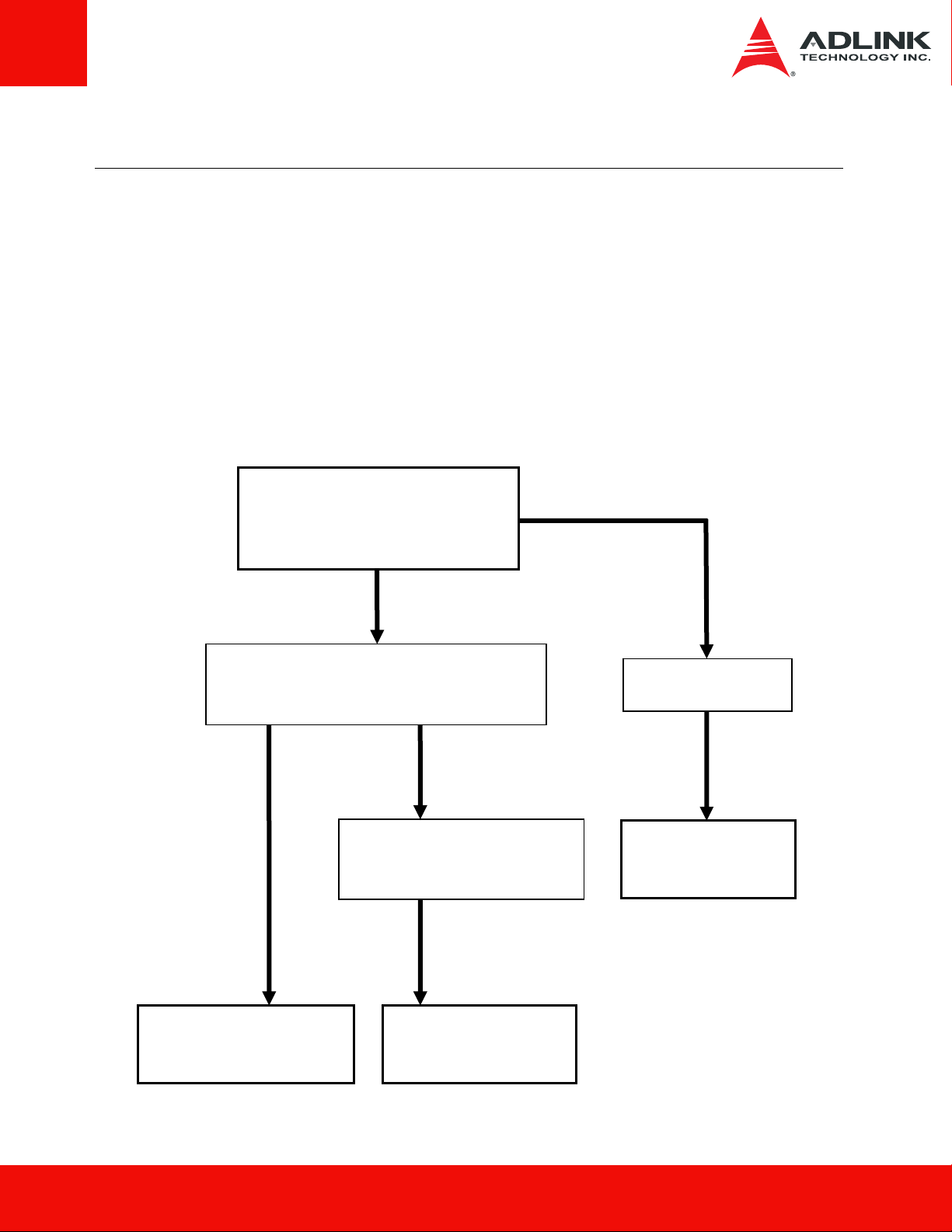
1.2 Functional Block Diagram
LVDS
LVDS Signal Input
from COM Express carrier
(CN4)
LVDS Signal Switch Array
(PI3USB20)
LVDS
LVDS-to-TTL Converter
(DS90CF386)
LVDS_SMCLK/SMDAT signals
PWM Circuitry
Backlight Control
(CN8)
TTL
LVDS Signal Output
(CN6)
TTL Signal Output
(CN5)
FPTB User's Manual 5
Page 6
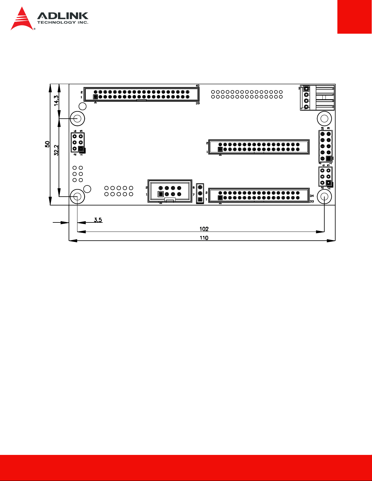
1.3 Mechanical Drawing
Dimensions in mm.
6 FPTB User's Manual
Page 7

1.4 Applications
The FPTB is intended for use in the following situations:
• nanoX/Express-BASE → FPTB → Customer’s cable to TTL display: This
configuration provides LVDS-to-TTL conversion and backlight control when using an
ADLINK reference carrier board with a TTL display. User must provide the cable
connection from the FPTB's TTL output and backlight control connectors to the TTL panel
inputs.
Backlight
control
TTL
Signal
LVDS-to-LVDS cable
ADLINK P/N: 30-20449-0000
LVDS output
TTL Display
nanoX/Express-BASE
Carrier Board
FPTB
5V and
12V Input
• Customer carrier (with LVDS output) → Customer’s cable to FPTB → HannStar
LVDS panel: This configuration provides backlight control and convenient verification of
LVDS function when using a customer carrier board with the HannStar 10.1” LVDS flat
panel display. User must provide the cable connection from the customer carrier board
LVDS output to the FPTB's LVDS input connector.
Backlight
LVDS output
Customer
FPTB
5V and
12V Input
control
LVDS
signal
ADLINK P/N: 30-20243-2000
ADLINK P/N: 29-90100-F000
Carrier Board
FPTB User's Manual 7
Page 8

• Customer carrier (with LVDS output) → Customer’s cable to FPTB → FPTB →
Customer’s cable to TTL panel: This configuration provides LVDS-to-TTL conversion
and backlight control when using a customer carrier board with a TTL display. User must
provide the cable connections from the customer carrier board LVDS output to the
FPTB's LVDS input connector and from the FPTB's TTL output and backlight control
connectors to the TTL panel inputs.
Backlight
control
TTL
Signal
TTL Display
LVDS output
Customer
Carrier Board
FPTB
5V and
12V Input
• Customer carrier (with LVDS output) → Customer’s cable to FPTB → FPTB →
Customer’s cable to other LVDS panel: This configuration provides backlight control
when using a customer carrier board with a customer LVDS flat panel display. User must
provide the cable connection from the customer carrier board LVDS output to the FPTB's
LVDS input connector and from the FPTB's LVDS output and backlight control
connectors to the LVDS panel inputs.
Backlight
control
LVDS Display
LVDS output
Customer
Carrier Board
FPTB
12V Input
LVDS
Signal
5V and
8 FPTB User's Manual
Page 9

2 Connectors and Jumpers
2.1 Board Layout
FPTB (Flat Panel Transfer Board) Connector and Jumper Locations
Connector Description
CN1 Power Connector
CN4 LVDS Input Connector
CN5 TTL Output Connector
CN6 LVDS Output Connector
CN8 Backlight Control Connector
JP1 Backlight Voltage Jumper
JP2 Panel Voltage Jumper
JP4 LVDS/TTL Mode Selector Jumper
JP5 Backlight Control Mode Jumper
FPTB User's Manual 9
Page 10

2.2 Connector Pin Definitions
CN1: Power Connector (Floppy power connector)
Pin Signal
1 +5V
2 GND
3 GND
4 +12V
CN4: LVDS Input Connector (2x17 box header, 2.00 mm pitch)
Pin Signal Pin Signal
1 LVDS_CLK_A 2 LVDS_DTA_A
3 PNL_PWR 4 PNL_PWR
5 GND 6 LVDS_A-N0
7 LVDS_A-P0 8 VDD_EN
9 LVDS_A-N1 10 LVDS_A-P1
11 BL_EN_2 12 LVDS_A-P2
13 LVDS_A-N2 14 N.C
15 LVDS_ACLK _ N 16 LVDS_ACLK _ P
17 PNL_PWR 18 LVDS_A-P3
19 LVDS_A-N3 20 GND
21 LVDS_B-N0 22 LVDS_B-P0
23 GND 24 LVDS_B-N1
25 LVDS_B-P1 26 GND
27 LVDS_B-N2 28 LVDS_B-P2
29 GND 30 LVDS_BCLK _ P
31 LVDS_BCLK _ N 32 N.C
33 LVDS_B-P3 34 LVDS_B-N3
10 FPTB User's Manual
Page 11

CN5: TTL Output Connector (2x20 box header, 2.00 mm pitch)
Pin Signal Pin Signal
1 GND 2 FCLK
3 GND 4 FR0
5 FR1 6 FR2
7 GND 8 FR3
9 FR4 10 FR5
11 GND 12 FR6
13 FR7 14 FG0
15 GND 16 FG1
17 FG2 18 FG3
19 GND 20 FG4
21 FG5 22 GND
23 FG6 24 FG7
25 FB0 26 GND
27 FB1 28 FB2
29 FB3 30 GND
31 FB4 32 FB5
33 FB6 34 GND
35 FB7 36
37
39
VS
(VSYNC)
DE
(DATA ENBLE)
38 GND
40 GND
HS
(HSYNC)
FPTB User's Manual 11
Page 12

CN6: LVDS Output Connector (2x17 box header, 2.00 mm pitch)
Pin Signal Pin Signal
1 LVDS_CLK_A 2 LVDS_DTA_A
3 PNL_PWR 4 PNL_PWR
5 GND 6 LVDS_A-N0
7 LVDS_A-P0 8 VDD_EN
9 LVDS_A-N1 10 LVDS_A-P1
11 BL_EN_2 12 LVDS_A-P2
13 LVDS_A-N2 14 N.C
15 LVDS_ACLK _ N 16 LVDS_ACLK _ P
17 PNL_PWR 18 LVDS_A-P3
19 LVDS_A-N3 20 GND
21 LVDS_B-N0 22 LVDS_B-P0
23 GND 24 LVDS_B-N1
25 LVDS_B-P1 26 GND
27 LVDS_B-N2 28 LVDS_B-P2
29 GND 30 LVDS_BCLK _ P
31 LVDS_BCLK _ N 32 N.C
33 LVDS_B-P3 34 LVDS_B-N3
CN8: Backlight Control Connector (2x4 box header, 2.54 mm pitch)
Pin Signal Pin Signal
1
3
5
7
2
4
6
8
1 GND 2 PNL_PWR
3 BL_CTRL 4 GND
5 LVDS_BL_EN 6 GND
7 N.C. 8 BLK_PWR
12 FPTB User's Manual
Page 13

2.3 Jumper Settings
JP1: Backlight Voltage
JP2: Panel Voltage
Jumper Configuration
1 - 2 +12V
3 – 4 Reserved
5 – 6 +5V*
Jumper Configuration
1 - 2 +12V
JP4: LVDS/TTL Mode
Jumper Configuration
JP5: Backlight Control Mode
Jumper Configuration
3 – 4 Reserved
5 – 6 +5V
7 - 8 Reserved
9 - 10 +3.3V*
1 - 2 TTL Output Active
3 - 4 Reserved
5 - 6 LVDS Output Active*
1 - 2 BLCTRL_PWM *
2 - 3 BLCTRL_VTL
Note: * indicates default setting
FPTB User's Manual 13
Page 14

3 Getting Started
The example instructions below describe how to use the FPTB to connect an ADLINK
reference carrier board to a TTL display: In this configuration, the FPTB provides LVDS-to-
TTL conversion and backlight control. The user must provide the cable connection from the
FPTB's TTL output and backlight control connectors to the TTL panel inputs.
Backlight
control
TTL
Signal
LVDS-to-LVDS cable
ADLINK P/N: 30-20449-0000
LVDS output
TTL Display
nanoX/Express-BASE
Carrier Board
FPTB
5V and
12V Input
3.1 Jumper Settings
Make sure the Backlight Voltage jumper (JP1) and Panel Voltage jumper (JP2) are
correct for the display panel you are using.
Set the LVDS/TTL Mode jumper (JP4) to TTL Output Active (short pins 1-2).Set the
Backlight Control Mode jumper (JP5) to PWM or Voltage Level as appropriate for your
display.
14 FPTB User's Manual
Page 15

3.2 LVDS Input to FPTB
Use the LVDS-to-LVDS cable that came with the FPTB to connect the LVDS output
connector on the ADLINK carrier board (CN6 on nanoX-BASE) to the LVDS input connector
on the FPTB (CN4).
Plug the LVDS-to-LVDS cable into nanoX-BASE CN6
Plug the LVDS-to-LVDS cable connector into FPTB CN4
LVDS-to-LVDS cable
FPTB User's Manual 15
Page 16

3.3 TTL Output to Display Panel
Make the appropriate cable to connect the TTL Output Connector (CN5) and Backlight
Control Connector (CN8) on the FPTB to the target TTL display panel.
3.4 FPTB Power Connector
Connect the Floppy Drive power connector of your power supply to the FPTB Power
Connector (CN1).
3.5 Power Up the System
Assemble the rest of your system as required and power it on. An example nanoX-BASE
system with FPTB connected to a TTL display panel is shown below.
16 FPTB User's Manual
Page 17

Technical Support
Contact us should you require any service or assistance.
ADLINK Technology, Inc.
Address: 9F, No.166 Jian Yi Road, Zhonghe District
New Taipei City 235, Taiwan
新北市中和區建一路 166 號 9 樓
Tel: +886-2-8226-5877
Fax: +886-2-8226-5717
Email: service@adlinktech.com
Ampro ADLINK Technology, Inc.
Address: 5215 Hellyer Avenue, #110, San Jose, CA 95138, USA
Tel: +1-408-360-0200
Toll Free: +1-800-966-5200 (USA only)
Fax: +1-408-360-0222
Email: info@adlinktech.com
ADLINK Technology (China) Co., Ltd.
Address:
300 Fang Chun Rd., Zhangjiang Hi-Tech Park,
Pudong New Area, Shanghai, 201203 China
Tel: +86-21-5132-8988
Fax: +86-21-5132-3588
Email: market@adlinktech.com
ADLINK Technology Beijing
Address:
Rm. 801, Power Creative E, No. 1, B/D
Shang Di East Rd., Beijing, 100085 China
Tel: +86-10-5885-8666
Fax: +86-10-5885-8625
Email: market@adlinktech.com
ADLINK Technology Shenzhen
Address:
A1
2F, C Block, Bldg. A1, Cyber-Tech Zone, Gao Xin Ave. Sec. 7,
High-Tech Industrial Park S., Shenzhen, 518054 China
Tel: +86-755-2643-4858
Fax: +86-755-2664-6353
Email: market@adlinktech.com
LiPPERT ADLINK Technology GmbH
Address: Hans-Thoma-Strasse 11, D-68163, Mannheim, Germany
Tel: +49-621-43214-0
Fax: +49-621 43214-30
Email: emea@adlinktech.com
上海市浦 新 江高科技 芳春路 300 (201203)
北京市海淀 上地 路 1
深圳市南山 科技 南 高新南七道
2C
(518057)
盈力大E 座 801 室(100085)
字技
FPTB User's Manual 17
Page 18

ADLINK Technology, Inc. (French Liaison Office)
Address: 15 rue Emile Baudot, 91300 Massy CEDEX, France
Tel: +33 (0) 1 60 12 35 66
Fax: +33 (0) 1 60 12 35 66
Email: france@adlinktech.com
ADLINK Technology Japan Corporation
Address: 〒101-0045
神田 374
KANDA374 Bldg. 4F, 3-7-4 Kanda Kajicho,
Chiyoda-ku, Tokyo 101-0045, Japan
Tel: +81-3-4455-3722
Fax: +81-3-5209-6013
Email: japan@adlinktech.com
ADLINK Technology, Inc. (Korean Liaison Office)
Address: 서울시 서초구 서초동 1675-12 모인터빌딩 8 층
8F Mointer B/D,1675-12, Seocho-Dong, Seocho-Gu,
Seoul 137-070, Korea
Tel: +82-2-2057-0565
Fax: +82-2-2057-0563
Email: korea@adlinktech.com
ADLINK Technology Singapore Pte. Ltd.
Address: 84 Genting Lane #07-02A, Cityneon Design Centre,
Singapore 349584
Tel: +65-6844-2261
Fax: +65-6844-2263
Email: singapore@adlinktech.com
ADLINK Technology Singapore Pte. Ltd. (Indian Liaison Office)
Address: 1st Floor, #50-56 (Between 16th/17th Cross) Margosa Plaza,
Margosa Main Road, Malleswaram, Bangalore-560055, India
Tel: +91-80-65605817, +91-80-42246107
Fax: +91-80- 23464606
Email: india@adlinktech.com
ADLINK Technology, Inc. (Israeli Liaison Office)
Address: 6 Hasadna St., Kfar Saba 44424, Israel
Tel: +972-9-7446541
Fax: +972-9-7446542
Email: israel@adlinktech.com
東京都千代田 神田鍛冶町 3-7-4
4F
18 FPTB User's Manual
 Loading...