

Page 1

PCI-/cPCI-/LPCI-/LPCIe-
723X Series
32-CH Isolated Digital I/O Card
User’s Manual
Manual Rev. 4.05
Revision Date: June 24, 2008
Part No: 50-11037-1000
Advance Technologies; Automate the World.
Page 2

Copyright 2008 ADLINK TECHNOLOGY INC.
All Rights Reserved.
The information in this document is subject to change without prior
notice in order to improve reliability , design, and function and does
not represent a commitment on the part of the manufacturer.
In no event will the manufacturer be liable for direct, indirect, special, incidental, or consequential damages arising out of th e use or
inability to use the product or documentation, even if advised of
the possibility of such damages.
This document contains proprietary information protected by copyright. All rights are reserved. No part of this manual may be reproduced by any mechanical, elec tronic, or other means in a ny form
without prior written permission of the manufacturer.
Trademarks
NuDAQ, NuIPC, DAQBench are registered trademarks of ADLINK
TECHNOLOGY INC.
Product names mentioned herein are used for identification pur-
poses only and may be trademarks and/or registered trademarks
of their respective companies.
Page 3
Getting Service from ADLINK
Customer Satisfaction is top priority for ADLINK Technology Inc.
Please contact us should you require any service or assistance.
ADLINK TECHNOLOGY INC.
Web Site: http://www.adlinktech.com
Sales & Service: Service@adlinktech.com
TEL: +886-2-82265877
FAX: +886-2-82265717
Address: 9F, No. 166, Jian Yi Road, Chungho City,
Taipei, 235 Taiwan
Please email or FAX this completed service form for prompt and
satisfactory service.
Company Information
Company/Organization
Contact Person
E-mail Address
Address
Country
TEL FAX:
Web Site
Product Information
Product Model
OS:
Environment
M/B: CPU:
Chipset: BIOS:
Please give a detailed description of the problem(s):
Page 4

Page 5

Table of Contents
Table of Contents..................................................................... i
List of Tables.......................................................................... iii
List of Figures........................................................................ iv
1 Introduction ........................................................................ 1
1.1 Features............................................................................... 2
PCI-7230, cPCI-7230, LPCI-7230, and LPCIe-7230 Fea-
tures ..................................................................... 2
PCI-7233 Features ........... ... ... ... .... ... ... ... ... .... ... ... ... .... ... . 2
PCI-7234/7234P Features .............................................. 3
1.2 PCI-7230/cPCI-7230/LPCI-7230/LPCIe-7230
Specifications ............................................................ 4
Isolated Digital I/O (DIO) ................................................. 4
General Specifications ....................................................5
1.3 PCI-7233 Specifications ...................................................... 6
Isolated Digital Input ....................................................... 6
General Specifications ....................................................6
1.4 PCI-7234/7234P Specifications........................................... 7
Isolated Digital Output ....................................................7
General Specifications ....................................................7
1.5 Software Support................................................................. 8
Windows Drivers ..... .......................................... ... ... .... ... . 9
Linux Drivers ................................................................. 14
Third-party Software Support .................................. .... .. 15
VEE™ Interface for ADLINK DAQ Cards .....................17
Componentware/ActiveX Control ..................................18
Applications for Test and Measurement ....................... 19
2 Installation ........................................................................ 21
2.1 What You Have.................................................................. 21
2.2 Unpacking.......................................................................... 21
2.3 Hardware Installation Outline............................................. 22
PCI configuration ........................................... ... ... ... .... .. 22
PCI slot selection ................. ... ... .... ... ............................ 22
2.4 Device Installation for Windows Systems.......................... 23
2.5 Connector Pin Assignment ................................................ 24
Table of Contents i
Page 6

PCI-7230 Pin Assignment .............................................24
cPCI-7230 Pin Assignment ............................. .... ... ... ... .26
LPCI/LPCIe-7230 Pin Assignment ................................28
PCI-7233 Pin Assignment .............................................30
PCI-7234 Pin Assignment .............................................32
PCI-7234P Pin Assignment ..........................................34
2.6 Termination Board Connection.......................................... 36
3 Register Format ................................................................ 37
3.1 PCI PnP Registers............................................................. 37
3.2 I/O Registers Format.......................................................... 38
3.3 Digital Input Register.......................................................... 39
3.4 Digital Output Register....................................................... 40
4 Operation Theory.............................................................. 41
4.1 Isolated Digital Input Circuits ............................................. 41
4.2 Isolated Digital Output Circuits........................................... 43
4.3 Change of State Detection................................................. 46
What is COS? ...............................................................46
Structure of COS detection and Dual Interrupt System 46
COS Detection ..............................................................48
ii Table of Contents
Page 7

List of Tables
Table 3-1: I/O Address Map of PCI-7230/cPCI-7230/LPCI-7230/LP-
CIe-7230 ...................................... ........................... 38
Table 3-2: I/O Address Map of PCI-7233 ................................ 38
Table 3-3: I/O Address Map of PCI-7234/7234P ..................... 38
Table 3-4: Digital Input Register .............................................. 39
Table 3-5: Digital Output Register ........................................... 40
Table 4-1: Differential Input circuits of cPCI-7230/LPCI-7230/LPCIe-
7230 ...................................... ................ ................. . 42
List of Tables iii
Page 8

List of Figures
Figure 2-1: PCI-7230 Pin Assignment..................... ... ... .... ... ... ... 24
Figure 2-2: PCI-7230 Onboard Power and Ground terminal...... 25
Figure 2-3: cPCI-7230 Pin Assignment...................................... 26
Figure 2-4: LPCI/LPCIe-7230 Pin Assignment........................... 28
Figure 2-5: PCI-7233 Pin Assignment..................... ... ... .... ... ... ... 30
Figure 2-6: PCI-7233 Onboard Power and Ground terminal...... 31
Figure 2-7: PCI-7234 Pin Assignment..................... ... ... .... ... ... ... 32
Figure 2-8: PCI-7234 Onboard Power and Ground terminal...... 33
Figure 2-9: PCI-7234P Pin Assignment............................ ... ... ... 34
Figure 2-10: PCI-7234P Onboard Power and Ground terminal... 35
Figure 4-1: Input circuits of 7230 and 7233 series..................... 41
Figure 4-2: Isolate output circuits of PCI-7234 (sink current)..... 43
Figure 4-3: Isolate output circuits of PCI-7234P (source curren t) 43
Figure 4-4: Isolation Output to TTL Input connection................. 44
Figure 4-5: Isolation Output to Isolation Input connection.......... 45
Figure 4-6: Dual Interrupt System of PCI-7233.......................... 47
Figure 4-7: Example of COS detection ...................................... 48
iv List of Figures
Page 9

1 Introduction
This manual lists and describes the components of the PCI-723X
family products, which includes:
X PCI-7230: Isolated 16-CH DI and 16-CH DO Card
X PCI-7233: Isolated 32-CH DI Card with COS detection
X PCI-7234: Isolated 32-CH DO Card
X PCI-7234P: Isolated 32-CH DO Card with Source Current
Transistor
X cPCI-7230: Isolated 16-CH DI and 16-CH DO Module for
3U CompactPCI
X LPCI-7230: Isolated 16-CH DI and 16-CH DO Card for low-
profile PCI
X LPCIe-7230: Isolated 16-CH DI and 16-CH DO Card for
low-profile PCI Express
These products have high isolation voltage with either 32 DI or 32
DO channels. The high isolation voltage protects the user’s computer against damage caused by accidental contact with high
external voltage and eliminates troublesome ground loops.
The PCI-7230/cPCI-7230/LPCI-7230/LPCIe-7230 provides 16 isolated inputs and 16 isolated outputs. The PCI-7230/cPCI-7230 isolated I/O channels are isolated to 5000 Vrms, and LPCI/LPCIe7230 isolated I/O channels are isolated to 2500 Vrms (excluding
cables).
The PCI-7233 provides 32 isolated digital input channels with
COS (change-of-state detection).
The PCI-7234/7234P provides 32 isolated digital output (Darlington transistor) channels. The isolation voltage is high up to 5,000
Vrms (excluding cables), both channel-to-channel and channel-tocomputer. (PCI-7 234 is sink cu rrent D O card , PCI-7234 P is sour ce
current DO card).
The PCI-7230/7233/7234 use ASIC PCI controller to interface the
board to the PCI bus. The ASIC fully implement the PCI local bus
specification Rev 2.1. All bus relative configurations, such as base
memory address and interrupt assignment, are automatically controlled by BIOS software. It does not need any user inter action and
Introduction 1
Page 10

pre-study for the configurations. This removes the burden of
searching for a conflict-free configuration, which can be very timeconsuming and difficult with some other bus standards.
1.1 Features
PCI-7230, cPCI-7230, LPCI-7230, and LPCIe-7230 Features
X Supports a 32-bit 5 V PCI bus (PCI-7230)
X 3U Eurocard form factor, CompactPCI Compliant (PICMG
2.0 Rev 2.1) (cPCI-7230)
X Support a 32-bit 3.3 V or 5 V PCI bus (LPCI-7230)
X x1 lane PCI Express Interface (LPCIe-7230)
X 16 isolated Digital Input Channels
X 16 isolated Digital Output Channels
X High output driving capability
X 5000 Vrms high volta ge isolation (for PCI-7230 and cPCI-
7230), 2500 Vrms high volt age isol ation (for LP CI-7230 and
LPCIe-7230)
X Two external interrupt sources
X 500 mA max@ 100% duty, for one of the eight transistor
devices ON
X Up to 24V voltage protection for isolated input
X 37-pin D-type connector (for PCI-7230)
X 50-pin SCSI-II type connector (for cPCI-7230, LPCI-7230,
and LPCIe-7230)
PCI-7233 Features
X 32 Isolated Digital Input Channels
X 5000 Vrms high voltage isolation
X Up to 24 V voltage protection for isolated input
X Interrupt is generated by COS (change-of-state) detection
X Dual interrupt trigger
X 37-pin D-type connector
2 Introduction
Page 11

PCI-7234/7234P Features
X 32 Isolated Digital Output Channels
X High output driving capability
X 500 mA max@ 100% duty, for one of the eight transistor
devices ON (PCI-7234: sink current, PCI-7234P: source
current)
X 5,000 Vrms high voltage isolation
X 37-pin D-type connector
Introduction 3
Page 12

1.2 PCI-7230/cPCI-7230/LPCI-7230/LPCIe-7230 Specifications
Isolated Digital I/O (DIO)
X Optical Isolated Input Channel
X Numbers of Channel: 16 digital inputs
X Input Vo ltage: up to 24Vdc
Z Logic “L”: 0 to 1.5 V
Z Logic “H”: 5 to 24 V
X Input resistance:1.2 KΩ @ 0.5 W
X Isolated voltage: 5000 Vrms (for PCI-7230 and cPCI-7230),
2500 Vrms (for LPCI-7230 and LPCIe-7230)
X Throughput:10 KHz
X Optical Isolated Output channel:
Z Numbers of Channel: 16 digital outputs
Z Output type: Darlington transistors
Z Output Voltage: open collector 5 V
35 V
X Sink Current:
Z 500 mA max @ 100% duty , for one of the eight transistor
(max.)
DC
devices ON
Z 370 mA @ duty 10% for all transistors devices ON
Z 130 mA @ duty 50% for all transistors devices ON
(Note: the pulse width is 25 ms for one duty cycle.)
X Throughput: 10 KHz
X Interrupt sources: Channel 0 and channel 1 of digital input
channels
(min.), up to
DC
4 Introduction
Page 13

General Specifications
X Connector:
Z 37-pin D-type connector for PCI-7230
Z 50-pin SCSI-II type connector for cPCI-7230, LPCI-
7230, and LPCIe-7230
X Operating Temperature: 0 to 60°C
X Storage Temperature: -20 to 80°C
X Humidity: 5 to 95%, non-condensing
X Power Consumption:
Z PCI-7230: +5V @ 150 mA (typical)
(Note: Requires external power)
Z cPCI-7230: +5V @ 270 mA (typical)
Z LPCI-7230: +5 V @ 150 mA (typical)
Z LPCIe-7230: +3.3 V @ 279 mA (typical)
+12 V @ 133 mA (typical)
X Dimension: Compact size, not including connectors
Z PCI-7230: 153mm(L) X 107mm(H)
Z cPCI-7230: 160 mm(L) X 100 mm(H)
Z LPCI-7230: 120 mm(L) X 65 mm(H)
Z LPCIe-7230: 119.9 mm(L) x 68.9 mm(H)
Introduction 5
Page 14

1.3 PCI-7233 Specifications
Isolated Digital Input
Optical Isolated Input
X Numbers of Channel: 32 digital inputs
X Input Vo ltage: up to 24Vdc
Z Logic “L”: 0 to 1.5V
Z Logic “H”: 5 to 24V
X Input resistance:1.2 KΩ @ 0.5W
X Isolated voltage: 5000Vrms
X Throughput: 10KHz
X Dual-interrupt sources:
Z Change-of-state (COS) on any 16 DI lines of LSB
Z Change-of-state (COS) on any 16 DI lines of MSB
General Specifications
X Connector: 37-pin D-type connector
X Operating Temperature: 0°C to 60°C
X Storage Temperature: -20°C to 80°C
X Humidity: 5 to 95%, non-condensing
X Power Consumption: +5V @ 300 mA
X Dimension: Compact size only 158 mm x 107 mm
6 Introduction
Page 15

1.4 PCI-7234/7234P Specifications
Isolated Digital Output
X Numbers of Channel: 32 digital output
Z Output type: Darlington transistors
Z Output Voltage: open collector 5 V
DC
(max.)
35 V
X Sink Current: (PCI-7234)
Z 500 mA max @ 100% duty, for one of the eight transis-
tors ON
Z 500 mA @ duty 20% for all transistors devices ON
(Note: the pulse width is 25ms for one duty cycle)
X Source Current:(PCI-7234P)
Z 500 mA max @ 100% duty, for one of the eight transis-
tors ON
Z 260 mA @ duty 10% for all transistors devices ON
(Note: the pulse width is 25 ms for one duty cycle)
X Isolated voltage:
Z 5000 Vrms
X Throughput:
Z 10 KHz
(min.), up to
DC
General Specifications
X Connector: 37-pin D-type connector
X Operating Temperature: 0 to 60°C
X Storage Temperature: -20 to 80°C
X Humidity: 5 to 95%, non-condensing
X Power Consumption: +5V @ 180 mA (typical, with internal
DC-DC power)
X Dimensions: 175 mm(H) x 107 mm(L)
Introduction 7
Page 16
1.5 Software Support
ADLINK Technology Inc., a leading provider of high-performance,
high-quality data acquisition cards and platforms, delivers robust
software support for its comprehensive line of DAQ cards with
varying form factors including PCI Express®, PCI, CompactPCI,
and PXI. ADLINK offers support not only f or m ainst re am Windows
and Linux OS, but also for third-party applications including LabVIEW® and MATLAB®. In addition, ADLINK also provides ActiveX
componentware for measurement and SCADA/HMI, and breakthrough proprietary software applications.
ADE
Library
Driver
Operating System Windows 98/NT/2K/XP/Vista x86 Windows XP x64/Server 2003 x64/Vista x64
ADLINK DAQ Cards
(General-Purpose DAQ, Digital I/O, Analog Output, Performance DAQ, PXI, High-Speed Digital I/O, Digitizer)
VB.NET/C#.NET/VC++/VB/Delphi/BCB etc.
DAQBench
PCIS-/D2K-/WD-OCX
ActiveX Control
D2K-/PCIS-/WD-DASK
DAQPilot
ActiveX Control
.NET Assembly
DAQPilot Drivers
(Task-oriented)
LabVIEW MATLAB
ADLINK
DAQ-VI EWPnP
VI Library
ADLINK
DAQ-MTLB
DAQ Toolbox
DAQMaster
Configuration
based
System Manager
For ADLINK
DAQ Devices
2
8 Introduction
Page 17
Windows Drivers
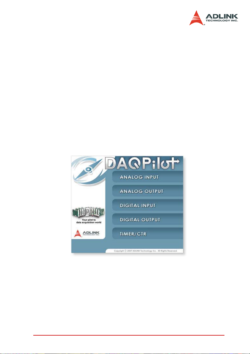
ADLINK Task-oriented DAQ Driver/SDK and Wizard for Windows
DAQPilot provides one interface for all ADLINK DAQ products via
X DAQPilot API
X DAQPilot ActiveX Control
X DAQPilot .Net Assembly,
DAQPilot (Download and install from the DAQPilot product page:
http://www.adlinktech.com/TM/DAQPilot.html
X Save development time
X Shorten learning curve
DAQPilot is a driver and SDK with a graphics-driven interface for
various ADE. DAQPilot comes as ADLINK's commitment to provide full support to its comprehensive line of data acquisition products. DAQPilot is designed for the beginners as well as
experienced programmers. Moreover, because DAQPilot can finish a DAQ task in minutes, it is suitable for programmers aiming to
Introduction 9
Page 18

immediately program ADLINK DAQ modules and integrate tasks
to their own DAQ applications.
Note: ADLINK strongly recommend all users to install the new-
generation ADLINK Driver – DAQPilot instead legacy DASK
drivers. For those users who have been usin g th e leg acy
ADLINK DASK Drivers or are not able to connect to the internet, you still can get the latest update from ADLINK all-inone CD.
10 Introduction
Page 19

Configuration-Based Device Manager for ADLINK DAQ Cards
X DAQMaster (.\Utility)
The ADLINK DAQMaster is a smart device manager that enables
access to ADLINK data acquisition and test and measurement
products. DAQMaster delivers an all-in-one configurations, user
can get a full support matrix to well configure ADLINK Test and
Measurement products.
DAQMaster enables you to:
X Manage ADLINK devices and interfaces
X Manage ADLINK installed software
X Manage ADLINK DAQPilot tasks
Introduction 11
Page 20

ADLINK Legacy DAQ Card Drivers and SDK for Windows
X PCIS-DASK (.\Software Package\PCIS-DASK)
X D2K-DASK (.\Software Package\D2K-DASK)
X WD-DASK (.\Software Package\WD-DASK)
Delphi
BCB
User Mode
PCIS-DASK
Kernel
Mode
Process
Structure
Object
Manager
DASK Kernel Driver
(.sys)
VC++
VB
VB.NET
C#
D2K-DASK
WD-DASK
Memory
Manager
System Service
Configuration
Manager
I/O Manager File System
Plug and Pay
Executive
Support
Power
Manager
Lowest-level
Driver
Hardware
Hardware Abstraction Layer
ADLINK's DASK are advanced 32-bit kernel drivers for customized DAQ application development. DASK enables users to perform detailed operations and achieve superior performance and
reliability from their data acquisition system. DASK kernel drivers
now support Windows Vista.
X PCIS-DASK for NuDAQ PCI/cPCI Series
X D2K-DASK for DAQ-2000 and PXI-2000 Series
X WD-DASK for High-speed Waveform Digitizer
12 Introduction
Page 21

DASK also supports the following:
X Supports Windows Vista 32- or 64-bit editions
X Supports AMD64 and Intel x86-64 architectures
X Digitally-signed for Windows Vista 64-bit Edition
X Utilizes WOW64 subsystem to ensure that 32-bit applica-
tions run normally on 64-bit Editions of Windows XP, Windows 2003 Server, and Windows Vista without modification.
More information about Windows Vista Support, please visit http://
www.adlinktech.com/TM/VistaSupport.html.
Note: Please use PCIS-DASK with the LPCI-7230 and LPCIe-
7230
Introduction 13
Page 22

Linux Drivers
Linux Drivers for ADLINK DAQ Cards
Drivers are available on the ADLINK website:
X PCIS-DASK/X
X D2K-DASK/X
X WD-DASK/X
ADLINK's DASK/X drivers are intended for developing customized
data acquisition applications under Linux environments. The
DASK/X drivers provide common APIs for ADLINK's extensive
family of PCI, CompactPCI, and PXI plug-in data acquisition
cards, and utilize the full capabilities of these cards under Linux
environment.
X PCIS-DASK/X for NuDAQ PCI/cPCI Series
X D2K-DASK/X for DAQ-2000 and PXI-2000 Series
X WD-DASK/X for ADLINK High-speed W aveform Digitizer
More information about Linux drivers, please visit http://
www.adlinktech.com/TM/linux_daq.html
Note: Please use PCIS-DASK/X with the LPCI-7230 and LPCIe-
7230
14 Introduction
Page 23

Third-party Software Support
MA T LAB® Data Acquisition Toolbox Adapter for ADLINK DAQ
Cards
X DAQ-MTLB for MATLAB® (.\Software Package\DAQ-
MTLB)
The DAQ-MTLB for MATLAB® integrates
ADLINK components with MATLAB® Data
Acquisition Toolbox and enables users to contro l
a wide range of ADLINK DAQ cards directly
from the advanced MATLAB® environment.
X Directly control scores of ADLINK DAQ
cards that come in different form factors including PCI
Express®, PCI, cPCI, and PXI
X Compliant with MA TLAB DAQ Toolbox 2.2 or higher (now at
R2007a)
X Critical updates and support are availa ble as AD LI NK is
now a MathWorks Connections Program partner
X ADLINK offers the only MATLAB® adapter for high-speed
digitizers with up to 65 MHz sampling rate and 14-bit resolution
More information, please visit http://ww w.adlinktech.com/TM/
DAQ-MTLB.html
Introduction 15
Page 24

LabVIEW™ Data Acquisition VI Set for ADLINK DAQ Cards
X DAQ Cards DAQ-LVIEW PnP for LabVIEW™ (.\Software
Package\DAQ-LVIEW PnP)
The DAQ-LVIEW PnP is a set of LabView Virtual Instruments (Vis)
that is fully-compatible with National Instrument's DAQ VIs. Based
on the virtual instruments concept, DAQ-LVIEW PnP provides four
additional tool panels in LabView, including analog input, analog
output, digital I/O, and timer/counter.
The DAQ-LVIEW PnP is designed and verified for LabVIEW 7.0,
and is compatible with LabVIEW 6.5, 7.1, 8.0, 8.2 and 8.5.
More information, please visit http://www.adlinktech.com/TM/labview-pnp.html
16 Introduction
Page 25

VEE™ Interface for ADLINK DAQ Cards
X PCIS-VEE (.\Software Package\PCIS-VEE)
X D2K-VEE (.\Software Package\D2K-VEE)
Agilent VEE™ is a popular visual programming environment for
data acquisition that includes data analysis and control. VEE provides a visual programming interface that allows users to create
programs by connecting objects such as acquisition routines, buttons and displays in a flow diagram. For users that are familiar
with Agilent VEE, ADLINK has released the PCIS-VEE and D2KVEE for seamless integration of the following NuDAQ data acquisition cards to the VEE environment:
X PCIS-VEE.
VEE for ADLINK NuDAQ Series DAQ cards
6208, 6308, 7200, 7230, 7233, 7234, 7250, 7252, 7248, 7249,
7296, 7300, 7396, 7432, 7433, 7434, 9111, 9112, 9113, 9114,
9118, 9812
X D2K-VEE.
VEE for DAQ-2000 Series DAQ cards
2010, 2005, 2006, 2204, 2205, 2206, 2501, 2502
The ADLINK PCIS-VEE and D2K-VEE drivers are designed and
verified for Agilent VEE 4.5 environment.
Introduction 17
Page 26

Componentware/ActiveX Control
32-Bit ActiveX Controls for Measurement and SCADA/HMI
DAQBench (.\Software Package\DAQBench)
DAQBench is a specialized ActiveX control package designed for
32-bit measurement and SCADA/HMI applications. DAQBench
leverages the power of the latest Microsoft ActiveX technology the standard for code interchangeability and integration under various Windows platform. With DAQBench, programmers can take
advantage of their familiarity with development environments such
as Visual Basic, Visual C++, Delphi, and Borland C++ Builder to
build their own applications.
18 Introduction
Page 27

Applications for Test and Measurement
Smart & Easy-to-Use Data Acquisition System Creator
DAQCreator (.\Software Package\DAQCreator)
DAQCreator is an out-of-the-box data acquisition software for
acquiring, displaying, analyzing, and storing data from ADLINK
DAQ cards. Equipped with a smart wizard and intuitive panels,
users can easily configure data acquisition settings, change the
appearance of data display, perform FFT to acquired data, and
store data to a hard disk drive. Another remarkable feature of
DAQCreator is the 40 MB/s stream-to-disk data throughput made
possible through combination with advanced SCSI technology.
DAQCreator delivers a cost-effective solution for high-speed data
logging applications.
Get latest ADLINK Software Solutions from ADLINK Web site:
http://www.adlinktech.com/TM/software-product.html
Note: All company names appearing herein are trademarks or
Note: Windows Vista is either a registered trademark or trademark
Introduction 19
trade names of their respective owners.
of Microsoft Corporation in the United States and/or other
countries.
Page 28

20 Introduction
Page 29

2 Installation
This chapter describes the configurations of the PCI-/cPCI-/LPCI-/
LPCIe-723X Series. The PCI-/cPCI-/LPCI-/LPCIe-723X Series is
Plug and Play and can easily be installed onto any PC system with
PCI slots.
2.1 What You Have
X This User’s Manual
X PCI-/cPCI-/LPCI-/LPCIe-723X Series Isolated Digital I/O
Card
X ADLINK CD
X Software Installation Guide
If any of these items are missing or damaged, please contact the
dealer from whom the product was purchased. Save the shipping
materials and carton for future storage or shipping purposes.
2.2 Unpacking
Your PCI-/cPCI-/LPCI-/LPCIe-723X Series card contains sensitive
electronic components that can be easily damaged by static electricity.
The card should be placed on a grounded anti-static mat. The
operator should wear an anti-static wristband, grounded at the
same point as the anti-static mat. Inspect the card module carton
for obvious damage. Shipping and handling may ca use dama ge to
the module. Ensure that there are no shipping and handing damages on the module before processing.
After opening the card module carton, extract the system module
and place it only on a grounded anti-static surface component side
up.
Again, inspect the module for damage. Press down on all socketed ICs to make sure they are properly seated. Do this only with
the module placed on a firm flat surface.
Note: Do not apply power to the card if it has been damaged.
Installation 21
Page 30

2.3 Hardware Installation Outline
PCI configuration
The PCI cards (or CompactPCI cards) are equipped with a Plug
and Play PCI controller, it can request base addresses and interrupt in accordance with the PCI standard. The system BIOS will
install the system resource based on the PCI cards’ configuration
registers and system parameters (which are set by syste m BIOS).
Interrupt assignment and memory usage (I/O port locations) of the
PCI cards can be assigned by system BIOS only. These system
resource assignments are done on a board-by-board basis. It is
not recommended that the system resource be assigned by any
other method.
PCI slot selection
The PCI card can be inserted into any PCI slot without any configuration for system resource.
Installation Procedures
1. Turn off the computer.
2. Turn off all accessories (printer, modem, monitor, etc.)
connected to your computer.
3. Remove the computer cover.
4. Select a 32-bit PCI slot. PCI slots are shorter than ISA or
EISA slots, and usually white or ivory in color.
5. Before handling the PCI cards, discharge any static
buildup on your body by touching the metal case of the
computer. Hold the edge and do not touch the compo-
nents.
6. Position the board into the selected PCI slot.
7. Secure the card in place at the rear panel of the system.
22 Installation
Page 31

2.4 Device Installation for Windows Systems
Once Windows Vista/XP/2003/200 0 has st arted, the Plug and Play
function of Windows system will find the new NuDAQ/NuIPC
cards. If this is the first time installing NuDAQ/NuIPC cards on
your Windows system, you will be prompted to enter the device
information source. Please refer to the “Software Installation
Guide” for instructions on installing the device.
Installation 23
Page 32

2.5 Connector Pin Assignment
PCI-7230 Pin Assignment
The pin assignment of the 37 pins D-type connector CN2, which is
an isolated DIO signal connector, shown below:
IDI_0
IDI_2
IDI_4
IDI_6
IDI_8
IDI_10
IDI_12
IDI_14
EICOM
EOGND
IDO_0
IDO_2
IDO_4
IDO_6
IDO_8
IDO_10
IDO_12
IDO_14
VDD
(1)
(2)
(3)
(4)
(5)
(6)
(7)
(8)
(9)
(10)
(11)
(12)
(13)
(14)
(15)
(16)
(17)
(18)
(19)
(20)
(21)
(22)
(23)
(24)
(25)
(26)
(27)
(28)
(29)
(30)
(31)
(32)
(33)
(34)
(35)
(36)
(37)
IDI_1
IDI_3
IDI_5
IDI_7
IDI_9
IDI_11
IDI_13
IDI_15
EOGND
EOGND
IDO_1
IDO_3
IDO_5
IDO_7
IDO_9
IDO_11
IDO_13
IDO_15
Figure 2-1: PCI-7230 Pin Assignment
24 Installation
Page 33

Legend:
IDI_n: Isolated digital input channel #n.
IDO_n: Isolated digital output channel #n.
EICOM: Common Ground or Common power of isolated input
channels.
EOGND: Ground return path of isolated output channels.
VDD: Power supply of isolated output channels.
Note:
The VDD must be supplied by an external power supply of 5 to 35VDC.
E O G N D
Figure 2-2: PCI-7230 Onboard Power and Ground te rminal
1 2
E O G N D
Installation 25
Page 34

cPCI-7230 Pin Assignment
The pin assignment of the cPCI-7230’s 50 pins SCSI-II type connector CN1 is shown in the following diagram.
VDD
EOGND
EOGND
EOGND
IDO_ 7
IDO_ 6
IDO_ 5
IDO_ 4
IDO_ 3
IDO_ 2
IDO_ 1
IDO_ 0
IDI_3 H
IDI_3 L
IDI_2 H
IDI_2 L
IDI_1 H
IDI_1 L
IDI_0 H
IDI_0 L
IDI_11
IDI_10
IDI_9
IDI_8
(1)
(2)
(3)
(4)
(5)
(6)
(7)
(8)
(9)
(10)
(11)
(12)
(13)
(14)
(15)
(16)
(17)
(18)
(19)
(20)
(21)
(22)
(23)
(24)
(25)
(26)
(27)
(28)
(29)
(30)
(31)
(32)
(33)
(34)
(35)
(36)
(37)
(38)
(39)
(40)
(41)
(42)
(43)
(44)
(45)
(46)
(47)
(48)
(49)
(50) EICOM
VDD
EOGND
EOGND
EOGND
IDO_14
IDO_15
IDO_12
IDO_13
IDO_10
IDO_11
IDO_ 8
IDO_ 9
IDI_7 L
IDI_7 H
IDI_6 L
IDI_6 H
IDI_5 L
IDI_5 H
IDI_4 L
IDI_4 H
IDI_1 5
IDI_1 4
IDI_1 3
IDI_1 2
EICOM
Figure 2-3: cPCI-7230 Pin Assignment
Legend:
IDI_n: Isolated digital input channel #n.
IDO_n: Isolated digital output channel #n.
26 Installation
Page 35

EICOM: Common ground or common power of isolated input
channels #8 to 15.
IDI_nH: High input of isolated differential DI channel #n.
IDI_nL: Low input of isolated differential DI channel #n.
EOGND: Ground return path of isolated output channels.
VDD: Power input signal for fly-wheel diode of DO channels.
Installation 27
Page 36

LPCI/LPCIe-7230 Pin Assignment
V
V
V
V
V
V
The pin assignment of the LPCI-7230’s 50 pins SCSI-II type connector CN1 is shown in the following diagram.
DD
DD
DD
VDD
EICOM
EOGND
EIGND
EIGND
EOGND
EIGND
EIGND
EICOM
EOGND
EIGND
EIGND
EICOM
IDO_7
IDO_7
IDO_ 7
IDO_7
IDO_6
IDO_6
IDO_6
IDO_ 6
IDO_5
IDO_5
IDO_ 5
IDO_5
IDO_4
IDO_4
IDO_ 4
IDO_4
IDO_3
IDO_3
IDO_ 3
IDO_3
IDO_2
IDO_2
IDO_ 2
IDO_2
IDO_1
IDO_1
IDO_1
IDO_ 1
IDO_0
IDO_0
IDO_ 0
IDO_0
IDI_3H
IDI_3H
IDI_3 H
IDI_3H
IDI_3 L
IDI_3L
IDI_3L
IDI_3L
IDI_2 H
IDI_2H
IDI_2H
IDI_2H
IDI_2 L
IDI_2L
IDI_2L
IDI_2L
IDI_1 H
IDI_1H
IDI_1H
IDI_1H
IDI_1 L
IDI_1L
IDI_1L
IDI_1L
IDI_0 H
IDI_0H
IDI_0H
IDI_0H
IDI_0 L
IDI_0L
IDI_0L
IDI_0L
IDI_11
IDI_11
IDI_11
IDI_11
IDI_10
IDI_10
IDI_10
IDI_10
IDI_9
IDI_9
IDI_9
IDI_9
IDI_8
IDI_8
IDI_8
IDI_8
OGND
EOGND
EOGND
(1)
(1)
(1)
(1)
(2)
(2)
(2)
(2)
(3)
(3)
(3)
(3)
(4)
(4)
(4)
(4)
(5)
(5)
(5)
(5)
(6)
(6)
(6)
(6)
(7)
(7)
(7)
(7)
(8)
(8)
(8)
(8)
(9)
(9)
(9)
(9)
(10)
(10)
(10)
(10)
(11)
(11)
(11)
(11)
(12)
(12)
(12)
(12)
(13)
(13)
(13)
(13)
(14)
(14)
(14)
(14)
(15)
(15)
(15)
(15)
(16)
(16)
(16)
(16)
(17)
(17)
(17)
(17)
(18)
(18)
(18)
(18)
(19)
(19)
(19)
(19)
(20)
(20)
(20)
(20)
(21)
(21)
(21)
(21)
(22)
(22)
(22)
(22)
(23)
(23)
(23)
(23)
(24)
(24)
(24)
(24)
(25)
(25)
(25)
(25)
(26)
(26)
(26)
(26)
(27)
(27)
(27)
(27)
(28)
(28)
(28)
(28)
(29)
(29)
(29)
(29)
(30)
(30)
(30)
(30)
(31)
(31)
(31)
(31)
(32)
(32)
(32)
(32)
(33)
(33)
(33)
(33)
(34)
(34)
(34)
(34)
(35)
(35)
(35)
(35)
(36)
(36)
(36)
(36)
(37)
(37)
(37)
(37)
(38)
(38)
(38)
(38)
(39)
(39)
(39)
(39)
(40)
(40)
(40)
(40)
(41)
(41)
(41)
(41)
(42)
(42)
(42)
(42)
(43)
(43)
(43)
(43)
(44)
(44)
(44)
(44)
(45)
(45)
(45)
(45)
(46)
(46)
(46)
(46)
(47)
(47)
(47)
(47)
(48)
(48)
(48)
(48)
(49)
(49)
(49)
(49)
(50) EICOM
(50)
(50)
(50)
VDD
VDD
VDD
VDD
ISO 5
ISO5
ISO5
ISO5V
EOGND
EIGND
EIGND
EICOM
EOGND
EIGND
EIGND
EICOM
IDO_14
IDO_14
IDO_14
IDO_14
IDO_15
IDO_15
IDO_15
IDO_15
IDO_12
IDO_12
IDO_12
IDO_12
IDO_13
IDO_13
IDO_13
IDO_13
IDO_10
IDO_10
IDO_10
IDO_10
IDO_11
IDO_11
IDO_11
IDO_11
IDO_8
IDO_ 8
IDO_8
IDO_8
IDO_ 9
IDO_9
IDO_9
IDO_9
IDI_7 L
IDI_7L
IDI_7L
IDI_7H
IDI_7 H
IDI_7H
IDI_7H
IDI_7L
IDI_6 L
IDI_6L
IDI_6L
IDI_6H
IDI_6 H
IDI_6H
IDI_6H
IDI_6L
IDI_5 L
IDI_5L
IDI_5L
IDI_5H
IDI_5 H
IDI_5H
IDI_5H
IDI_5L
IDI_4 L
IDI_4L
IDI_4L
IDI_4H
IDI_4 H
IDI_4H
IDI_4H
IDI_4L
IDI_1 5
IDI_15
IDI_15
IDI_15
IDI_1 4
IDI_14
IDI_14
IDI_14
IDI_1 3
IDI_13
IDI_13
IDI_13
IDI_1 2
IDI_12
IDI_12
IDI_12
EICOM
EOGND
EOGND
EOGND
Figure 2-4: LPCI/LPCIe-7230 Pin Assignment
Legend:
IDI_n: Isolated digital input channel #n.
IDO_n: Isolated digital output channel #n.
28 Installation
Page 37

EICOM: Common ground or common power of isolated input
channels #8 to 15.
IDI_nH: High input of isolated differential DI channel #n.
IDI_nL: Low input of isolated differential DI channel #n.
EOGND: Ground return path of isolated output channels.
VDD: Power input signal for fly-wheel diode of DO channels.
ISO5V: Isolatied power output 5V.
Installation 29
Page 38

PCI-7233 Pin Assignment
The pin assignment of the 37 pins D-type connector CN1 is illustrated below:
IDI_0
IDI_2
IDI_4
IDI_6
IGND
IDI_9
IDI_11
IDI_13
IDI_15
IDI_16
IDI_18
IDI_20
IDI_22
IGND
IDI_25
IDI_27
IDI_29
IDI_31
IGND
(1)
(2)
(3)
(4)
(5)
(6)
(7)
(8)
(9)
(10)
(11)
(12)
(13)
(14)
(15)
(16)
(17)
(18)
(19)
(20)
(21)
(22)
(23)
(24)
(25)
(26)
(27)
(28)
(29)
(30)
(31)
(32)
(33)
(34)
(35)
(36)
(37)
IDI_ 1
IDI_ 3
IDI_ 5
IDI_ 7
IDI_ 8
IDI_ 1 0
IDI_ 1 2
IDI_ 1 4
IGND
IDI_17
IDI_ 1 9
IDI_ 2 1
IDI_ 2 3
IDI_ 2 4
IDI_ 2 6
IDI_ 2 8
IDI_ 3 0
IGND
Figure 2-5: PCI-7233 Pin Assignment
Legend:
IDI_n: Isolated digital input channel n.
I.GND: Isolated common ground.
30 Installation
Page 39

I.GND
1 2
CN2
Figure 2-6: PCI-7233 Onboard Power and Ground te rminal
VDD
3 4
CN3
Installation 31
Page 40

PCI-7234 Pin Assignment
The pin assignment of the 37 pins D-type connector CN1, which is
an isolated DIO signal connector, is shown below.
IDO_0
IDO_2
IDO_4
IDO_6
I.GND
IDO_9
IDO_11
IDO_13
IDO_15
IDO_16
IDO_18
IDO_20
IDO_22
I.GND
IDO_25
IDO_27
IDO_29
IDO_31
VDD
(1)
(2)
(3)
(4)
(5)
(6)
(7)
(8)
(9)
(10)
(11)
(12)
(13)
(14)
(15)
(16)
(17)
(18)
(19)
(20)
(21)
(22)
(23)
(24)
(25)
(26)
(27)
(28)
(29)
(30)
(31)
(32)
(33)
(34)
(35)
(36)
(37)
IDO_1
IDO_3
IDO_5
IDO_7
IDO_8
IDO_10
IDO_12
IDO_14
I.GND
IDO_17
IDO_19
IDO_21
IDO_23
IDO_24
IDO_26
IDO_28
IDO_30
I.GND
Figure 2-7: PCI-7234 Pin Assignment
Legend:
IDO_n: Isolated digital output signal channel n.
I.GND: Isolated Ground for all isolated output channels.
VDD: Power input signal for fly-wheel diode of DO channels.
32 Installation
Page 41

VDD
I.GN
1
CN2 CN3
Figure 2-8: PCI-7234 Onboard Power and Ground te rminal
I.GND
3
1 2
CN2
VDD
3 4
CN3
Installation 33
Page 42

PCI-7234P Pin Assignment
The pin assignment of the 37 pins D-type connector CN1, which is
an isolated DIO signal connector, as shown below:
IDO_0
IDO_2
IDO-4
IDO_6
VDD
IDO_9
IDO_11
IDO_13
IDO_15
IDO_16
IDO_18
IDO_20
IDO_22
VDD
IDO_25
IDO_27
IDO_29
IDO_31
I.GND
(1)
(2)
(3)
(4)
(5)
(6)
(7)
(8)
(9)
(10)
(11)
(12)
(13)
(14)
(15)
(16)
(17)
(18)
(19)
(20)
(21)
(22)
(23)
(24)
(25)
(26)
(27)
(28)
(29)
(30)
(31)
(32)
(33)
(34)
(35)
(36)
(37)
IDO_1
IDO_3
IDO_5
IDO_7
IDO_8
IDO_10
IDO_12
IDO_14
VDD
IDO_17
IDO_19
IDO_21
IDO_23
IDO_24
IDO_26
IDO_28
IDO_30
VDD
Figure 2-9: PCI-7234P Pin Assignment
Legend:
IDO_n: Isolated digital output signal channel n.
I.GND: Isolated ground for isolated output channels.
VDD: External power supply for IDO source drivers.
34 Installation
Page 43

VDD
1 2
I.GND
VDD
3 4
1 2
I.GND
3 4
CN2 CN3
CN2
Figure 2-10: PCI-7234P Onboard Power and Ground terminal
CN3
Installation 35
Page 44

2.6 Termination Board Connection
The 723X boards are equipped with a DB-37 or a 50-pin SCSI-II
female connector. Available termination boards include:
ACLD-9137-01:
General-Purpose termination board with a 37-pin D-sub male connector.
DIN-37D-01:
Termination board with a 37-pin D-sub connector and DIN-Rail
mounting (including one 1-meter ACL-10137 cable).
DIN-50S-01:
Termination board with a 50-pin SCSI-II connector and DIN-Rail
mounting (including one 1-meter ACL-10250 cable)
36 Installation
Page 45

3 Register Format
The registers format is described in this chapter. This information
is quite useful for programmers who wish to handle the card by
low-level programming. However, it is recommended that the user
has a deeper understanding of the PCI interface before starting
any low-level programming. This chapter can also assist users in
using the software driver to manipulate this card.
3.1 PCI PnP Registers
This PCI card functions as a 32-b it PCI target device to any m aster on the PCI bus. There are three types of registers: PCI Configuration Registers (PCR), Local Configuration Registers (LCR),
and PCI-723X registers.
The PCR, which is compliant with the PCI-bus specifications, is
initialized and controlled by the Plug and Play PCI BIOS. Users
can study the PCI BIOS specification to understand the operation
of the PCR. Please contact the PCISIG for specifications of the
PCI interface.
The PCI bus controller PCI 9052 is provided by PLX technology
Inc. (www.plxtech.com). For further detail on the LCR, please visit
PLX technology’s website to download the relative information.
Users are not required to understand the details of the LCR if
using the software library. The PCI PnP BIOS assigns the base
address of the LCR to offset 14h of PCR.
The PCI-723X registers are shown in the next section. The base
address, which is also assigned by the PCI PnP BIOS, is located
at offset 18h of PCR. Therefore, users can read the 18h of PCR to
find the base address by using the BIOS function call.
Do not try to modify the base address and interrupt assigned by
the PCI PnP BIOS as it may cause resource conflict within your
system.
Register Format 37
Page 46

3.2 I/O Registers Format
The PCI-7230/cPCI-7230/LPCI-7230/LPCIe-7230 requires one
32-bit address in the PC I/O address space. Table 3.1 shows the I/
O address of each register with respect to the base address.
Address Write Read
Base (0 - 1 ) Isolated DO Isolated DI
Table 3-1: I/O Address Map of PCI-7230/cPCI-7230/LPCI-7230/LPCIe-7230
The PCI-7233 requires one 32-bit address in the PC I/O address
space. Table 3.2 shows the address.
Address Write Read
Base (0 - 3 ) -- Isolated DI
Table 3-2: I/O Address Map of PCI-7233
The PCI-7234/7234P requires one 32-bit address in the PC I/O
address space. Table 3.3 shows the address.
Address Write Read
Base (0 - 3 ) Isolated DO --
T able 3-3: I/O Address Map of PCI-7234/7234P
CAUTION:
All the I/O ports above are 32-bit width.
8-bit or 16-bit I/O access is NOT allowed.
38 Register Format
Page 47

3.3 Digital Input Register
There is a total of 16 and 32 digital input channels on the PCI7230/cPCI-7230/LPCI-7230/LPCIe-7230 and PCI-7233 respectively . Each bit correspond s to a signal on the digit al inpu t channel.
IDI_16 to IDI_31 are only available on PCI-7233.
Address: BASE + 0 to BASE + 3
Attribute: read only
Data Format:
Bit 7 6 5 4 3 2 1 0
Base + 0 IDI_7 IDI_6 IDI_5 IDI_4 IDI_3 IDI_2 IDI_1 IDI_0
Base + 1 IDI_15 IDI_14 IDI_13 IDI_12 IDI_11 IDI_10 IDI_9 IDI_8
Base + 2 IDI_23 IDI_22 IDI_21 IDI_20 IDI_19 IDI_18 IDI_17 IDI_16
Base + 3 IDI_31 IDI_30 IDI_29 IDI_28 IDI_27 IDI_26 IDI_25 IDI_24
Table 3-4: Digital Input Register
Legend:
IDI_n: Isolated Digital Input CH n.
Register Format 39
Page 48

3.4 Digital Output Register
There is a total of 16 and 32 digital output channels on the PCI7230/cPCI-7230/LPCI-7230/LPCIe-7230 and PCI-7234/7234P
respectively. Each bit corresponds to a signal on the digital output
channel. IDO_16 to IDO_31 are only available on PCI-7234/
7234P.
Address: BASE + 0 to BASE + 3
Attribute: write only
Data Format:
Bit 7 6 5 4 3 2 1 0
Base + 0 IDO_7 IDO_6 IDO_5 IDO_4 IDO_3 IDO_2 IDO_1 IDO_0
Base + 1 IDO_15 IDO_14 IDO_13 IDO_12 IDO_1 1 IDO_10 IDO_9 IDO_8
Base + 2 IDO_23 IDO_22 IDO_21 IDO_20 IDO_19 IDO_18 IDO_17 IDO_16
Base + 3 IDO_31 IDO_30 IDO_29 IDO_28 IDO_27 IDO_26 IDO_28 IDO_24
Table 3-5: Digital Output Register
Legend:
IDO_n: Isolated Digital Output CH n.
40 Register Format
Page 49

4 Operation Theory
4.1 Isolated Digital Input Circuits
The isolated digital output is an open collector transistor output.
The input can accept voltages of up to 24 V. The input resisters on
PCI-7230/7233, cPCI-7230 and LPCI-7230/LPCIe-7230 are
1.2 K
Ω. The connection between outside signal and PCI-7230/
7233, cPCI-7230 and LPCI-7230/LPCIe-7230 are shown below.
Isolated Input
EICOM
Isolated Input
EICOM
1.2K Ohm
GND
1.2K Ohm
GND
Figure 4-1: Input circuits of 7230 and 7233 series
Operation Theory 41
Page 50

DI_nH
1.2K Ohm
DI_nL
T able 4-1: Differential Input circuits of cPCI-7230/LPCI-7230/LPCIe-7230
42 Operation Theory
Page 51

4.2 Isolated Digital Output Circuits
On the 7230/7234 series, an external voltage source, minimum
5V, maximum 35 VDC, is necessary to power the internal isolated
circuits. It is connected with the VDD pin, When the isolated digital
output goes to high, the sink current will be from VDD.
On the 7230/7234 series, the VDD pin is used as a “fly-wheel”
diode, which can protect the driver if the loading is inductance
loading such as relay, motor, or solenoid.
The VDD must connect to the external power to form a fly-wheel
current loop.
V5V
VDD
DC (5-35V)
Load
+
IDOn
I.GND
Darlington
Sink Driver
PC 817
Figure 4-2: Isolate output circuits of PCI-7234 (sink current)
V5V
VDD
IDOn
DC (5-35V)
+
Load
I.GND
PC 817
Darlington
Source Current
Figure 4-3: Isolate output circuits of PCI-7234P (source current)
Operation Theory 43
Page 52

Figure 4-4: Isolation Output to TTL Input connection
44 Operation Theory
Page 53

Figure 4-5: Isolation Output to Isolation Input connection
Operation Theory 45
Page 54

4.3 Change of State Detection
What is COS?
The COS (Change of State) occurs when the input state (logic
level) is changed from low to high or from high to low. The COS
detection circuit is used to detect the edge of level change. In the
PCI-7233 card, the COS detection circuit is applied to all 32 channels input channels. If any channel is changed, the COS detection
circuit generates an interrupt request signal.
Structure of COS detection and Dual Interrupt System
The dual interrupt system is used in PCI-7233. Dual interrupt
occurs when the hardware can generate two interrupt request signals at the same time and the software can service these two
requests with ISR. Note that dual interrupt does not mean the card
occupies two IRQ levels. The two interrupt request signals (INT1
and INT2) come from COS detection output signal #1 and #2. The
INT1 is inserted when any channel from 0 to 15 is changed. The
INT2 is inserted when any channel between 16 to 31 is changed.
The interrupt system is illustrated below.
46 Operation Theory
Page 55

DI_0~
DI_31
DI_0~
DI_15
INT1
PLD1
32
Channel
Isolated
Input
DI_16~
DI_31
Clear
IRQ
INT2
PCI
Bridge
PLD2
Figure 4-6: Dual Interrupt System of PCI-7233
PCI Bus
Operation Theory 47
Page 56

COS Detection
The following timing is an example of the COS detection. Every DI
signal’s edge change can be detected. All the DI channels edge
will be ‘OR’ together to generate the INT1 or INT2 IRQ signals.
If INT1 or INT2 irq Signals generate, the signal will be latch its
state. The user can use the “_7233_CLR_IRQ” function to clear,
INT1, or INT2 IRQ signal state.
DI_0
DI_1
DI_0 COS
DI_1 COS
INT1
Clear_IRQ
Figure 4-7: Example of COS detection
48 Operation Theory
Clear_IRQ Clear_IRQ
 Loading...