

Page 1

LPCI/PXI-3488A
IEEE488 GPIB Interface Card Series
User’s Manual
Manual Rev. 2.00
Revision Date: May 15, 2008
Part No: 50-17023-3000
Advance Technologies; Automate the World.
Page 2

Copyright 2008 ADLINK TECHNOLOGY INC.
All Rights Reserved.
The information in this document is subject to change without prior
notice in order to improve reliability , design, and function and does
not represent a commitment on the part of the manufacturer.
In no event will the manufacturer be liable for direct, indirect, special, incidental, or consequential damages arising out of the use or
inability to use the product or documentation, even if advised of
the possibility of such damages.
This document contains proprietary information protected by copyright. All rights are reserved. No part of this manual may be reproduced by any mechanical, elec tronic, or other means in a ny form
without prior written permission of the manufacturer.
Trademarks
Product names mentioned herein are used for identification pur-
poses only and may be trademarks and/or registered trademarks
of their respective companies.
Page 3
Getting Service from ADLINK
Customer Satisfaction is top priority for ADLINK Technology Inc.
Please contact us should you require any service or assistance.
ADLINK TECHNOLOGY INC.
Web Site: http://www.adlinktech.com
Sales & Service: Service@adlinktech.com
TEL: +886-2-82265877
FAX: +886-2-82265717
Address: 9F, No. 166, Jian Yi Road, Chungho City,
Taipei, 235 Taiwan
Please email or FAX this completed service form for prompt and
satisfactory service.
Company Information
Company/Organization
Contact Person
E-mail Address
Address
Country
TEL FAX:
Web Site
Product Information
Product Model
OS:
Environment
M/B: CPU:
Chipset: Bios:
Please give a detailed description of the problem(s):
Page 4

Page 5

Table of Contents
1 Introduction ........................................................................ 1
1.1 Overview.............................................................................. 1
Performance ................................................................... 1
Compatibility ................................................................... 1
1.2 Features............................................................................... 3
LPCI-3488A .................................................................... 3
PXI-3488A ...................................................................... 3
1.3 Specifications....................................................................... 4
GPIB Bus Properties ....................................................... 4
Certificates ........................... ............................. .............. 4
General Specifications ....................................................5
1.4 Software Support................................................................. 6
2 Installation .......................................................................... 7
2.1 Contents of Package ................................... ... .... ... ... ... ....... 7
LPCI-3488A .................................................................... 7
PXI-3488A ...................................................................... 7
2.2 Unpacking............................................................................ 8
2.3 Mechanical Drawing ............................................................ 9
LPCI-3488A .................................................................... 9
PXI-3488A .................................................................... 10
2.4 PCI Configuration .............................................................. 11
Plug and Play ...............................................................11
Configuration ................................................................ 11
Troubleshooting ................................ ............................ 11
2.5 Hardware Installation................................. ... ... .... ... ... ... .... . 12
LPCI-3488A Installation Procedures ............................. 12
PXI-3488A Installation Procedures ......................... ......13
Cabling ......................................................................... 13
2.6 Software Installation .......................................................... 16
Driver installation .......................................................... 16
Using the ADLINK GPIB Utility ............................ ... .... .. 18
3 Operation Theory ............................................................. 21
3.1 Connection Configuration .................................................. 21
Data Lines .................... .... ... ... ... .... ... ... ... ... .... ... ............23
Handshake Lines ..........................................................23
System management lines ........................................... 23
Table of Contents i
Page 6

3.2 ADLINK GPIB Interface Cards Block Diagram .................. 24
ii Table of Contents
Page 7

List of Tables
Table 1-1: Power Requirements, LPCI-3488A .......................... 5
Table 1-2: Power Requirements, PXI-3488A ............................. 5
Table 3-1: GPIB Bus ................................................................ 22
List of Tables iii
Page 8

List of Figures
Figure 2-1: PCB Layout of the LPCI-3488A................................. 9
Figure 2-2: PCB Layout of the PXI-3488A ................................. 10
Figure 2-3: LPCI-3488A Linear Connection Configuration......... 14
Figure 2-4: LPCI-3488A Star Connection Configuration............ 14
Figure 2-5: PXI-3488A Linear Connection Configuration........... 15
Figure 2-6: PXI-3488A Star Connection Configuration .............. 15
Figure 3-1: Standard GPIB Connector....................................... 21
Figure 3-2: Block Diagram of ADLINK GPIB Interface Cards.... 24
iv List of Figures
Page 9

1 Introduction
1.1 Overview
ADLINK’s LPCI-3488A and PXI-3488A GPIB controller interface
cards are fully compatible with the IEEE488.2 instrumen tation co ntrol and communication standard and are capable of controlling up
to 14 stand-alone instruments via IEEE488 cables. The LPCI3488A and PXI-3488A are designed to meet the requirements for
high performance and maximum programming portability. They
were developed using ADLINK’s intellectual property in FPGAs
which incorporates the GPIB controller , provides reliable GPIB bus
control capability , and support s a transfer rate up to 1.5 MB/s. With
APIs that are compatible with National Instruments
VISA support, the LPCI-3488A and PXI-3488A offer the be st compatibility with your existing applications and instrument drivers.
1.1.1 Performance
ADLINK’s expertise in PCI and PXI interface cards was leveraged
when developing these newly designed GPIB interface card. The
LPCI-3488A, which is the low-profile PCI form factor, supports
both 3.3 V and 5 V PCI buses and can be adapted to most industrial and desktop computers. The PXI-3488A is compliant with PXI
specification Rev. 2.0 and can be used with most PXI and CompactPCI system. A 2 KB FIFO is placed between the GPIB bus
and PCI controller to buffer GPIB read/write operations. This FIFO
eliminates the gap between the slow GPIB bus (~1.5 MB/s) and
the fast PCI bus (132 MB/s), and dramatically increases overall
system performance.
1
software and
1.1.2 Compatibility
ADLINK’s GPIB interface solutions are delivered with complete
software support, including a driver API set that is fully binary com-
patible with NI
1. National Instruments is a registered trademark of National Instruments Corporation
2. NI is a registered trademark of National Instruments Corporation
Introduction 1
2
’s GPIB-32.DLL. All programs written based on the
Page 10

GPIB-32.DLL library can be executed with LPCI-3488A or PXI3488A without any modification. VISA library is also supported to
ensure compatibility with applications utilizing VISA. The ADLINK
LPCI-3488A and PXI-3488A thus provides the “Plug and Play”
compatibility with all your existing applications.
2Introduction
Page 11

1.2 Features
1.2.1 LPCI-3488A
The LPCI-3488A IEEE 488 GPIB interface card provides the following advanced features:
X Fully compatible with the IEEE 488 standard
X Up to 1.5 MB/s data transfer rates
X Built-in 2 KB FIFO for read/write operations
X Provides APIs compatible with NI-488.2
X Supports industrial-standard VISA Library
X Interactive utility for testing and diagnostics
X Fully low-profile MD1 PCB compliant
1.2.2 PXI-3488A
The PXI-3488A IEEE 488 GPIB interface card provides the following advanced features:
X PXI specifications Rev. 2.0 compliant
X 3U Eurocard form factor, CompactPCI compliant (PICMG
2.0 R3.0)
X Fully compatible with the IEEE 488 standard
X Up to 1.5 MB/s data transfer rates
X Built-in 2 KB FIFO for read/write operations
X Provides APIs compatible with NI-488.2
X Supports industrial-standard VISA Library
X Interactive utility for testing and diagnostics
1
driver software
1
driver software
1. NI-488.2 is a trademark of National Instruments Corporation.
Introduction 3
Page 12

1.3 Specifications
1.3.1 GPIB Bus Properties
X Up to 14 instruments can be connected to one controller
X Maximum 1.5 MB/s data transfer rate
X Cable length
Z 2 meters between each instrument (suggested)
Z 20 meters total cable length
X Data transfer mode: 8 bits parallel
X Handshake: 3 wire handshake, reception of each data byte
is acknowledged
1.3.2 Certificates
X EMC/EMI: CE, FCC Class A
4Introduction
Page 13

1.3.3 General Specifications
X I/O Connector: IEEE 488 standard 24-pin connector
X Operating temperature: 0 to 55ºC
X Storage temperature: -20 to 80ºC at 10 to 90% humidity
X Relative humidity: 10 to 90%, non-condensing
X Power requirements
Z LPCI-3488A
+5 V
250 mA (typical)
300 mA (maximum)
Table 1-1: Power Requirements, LPCI-3488A
Z PXI-3488A
+5 V
250 mA (typical)
300 mA (maximum)
Table 1-2: Power Requirements, PXI-3488A
X Dimensions (not including connectors) :
Z LPCI-3488A: 120 mm x 64 mm
Z PXI-3488A: 160 mm x 100 mm
Introduction 5
Page 14

1.4 Software Support
The ADLINK LPCI-3488A and PXI-3488A GPIB interface cards
provide a device driver package: ADL-GPIB for Windows 98/2000/
XP/Vista. The ADGPIB driver package also provides a diagnostic
utility to test GPIB interface cards, as well as programming samples and source code examples for Microsoft Visual C++. The
ADL-GPIB driver package can be found in the included All-in-one
CD. Please refer to the Software Installation section (2.6), o n p age
16 for detailed software installation instructions.
For other OS support, please contact ADLINK for more information.
6Introduction
Page 15

2 Installation
This chapter outlines the contents of package, describes unpacking information, and describes how to install the hardware and
software.
2.1 Contents of Package
2.1.1 LPCI-3488A
The LPCI-3488A includes the following items:
X LPCI-3488A
X An additional low-profile bracket
X ADLINK All-in-One CD
X This User’s Manual
2.1.2 PXI-3488A
The PXI-3488A includes the following items:
X PXI-3488A
X ADLINK All-in-One CD
X This User’s Manual
If any of these items are missing or damaged, contact your
ADLINK dealer. Please save the shipping materials and carton to
ship or store the product if needed.
Installation 7
Page 16

2.2 Unpacking
Both the LPCI-3488A and PXI-3488A contain electrostatic sensitive components that can be easily be damaged by static electricity.
Therefore, these modules should be handled on a grounded antistatic mat. The operator should be wearing an anti-static wristband, grounded at the same point as the anti-static mat.
Inspect the module for obvious damage. Shipping and handling
may cause damage to the module. Be sure there is no shipping
and handling damage on the module before continuing.
Note: DO NOT APPLY POWER TO THE CARD IF IT HAS BEEN
DAMAGED.
8Installation
Page 17

2.3 Mechanical Drawing
2.3.1 LPCI-3488A
Figure 2-1: PCB Layout of the LPCI-3488A
Installation 9
Page 18
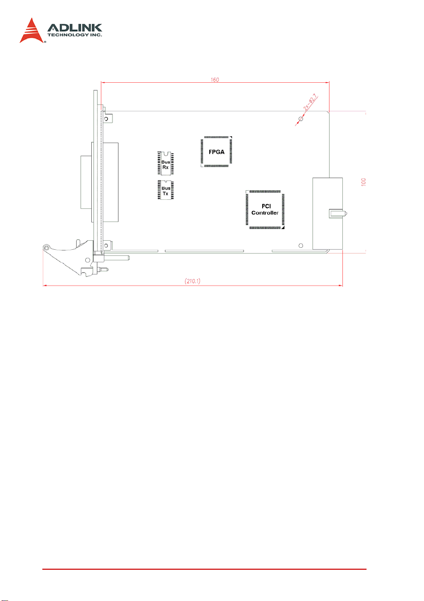
2.3.2 PXI-3488A
Figure 2-2: PCB Layout of the PXI-3488A
The ADLINK PXI-3488A is packaged in a Eurocard form factor
compliant with the PXI Specification and measuring 160 mm in
length and 100 mm in height (not including connectors). The
IEEE488 standard 24-pin connector is located at the front panel
and the J1 IEC connectors in the rear are used to link the chassis
backplane. With its modular, rugged, and high shock resistant
mechanical features, the IEEE488 GPIB Interface module functions exceptionally well in harsh environment applications.
10 Installation
Page 19

2.4 PCI Configuration
2.4.1 Plug and Play
As a plug-and-play component, the card requests an interrupt
number via its PCI controller. The system BIOS responds with an
interrupt assignment based on the card in format ion and on know n
system parameters. These system parameters are determined by
the installed drivers and the hardware is acknowledged by the system.
2.4.2 Configuration
Board configuration is accomplished on a board-by-board basis
for all PCI/PXI boards in the chassis. Because configuration is
controlled by the system and software, there is no jumper setting
required for base-address, DMA, and interrupt IRQ.
The configuration is subject to change with every boot of the system as new boards are added or removed.
2.4.3 Troubleshooting
If the system doesn’t boot or you experience erratic operation with
the PCI/PXI board in place, it’s likely caused by an interrupt conflict (perhaps the BIOS settings are incorrectly configured). In general, the solution, once you determine it is not a simple oversight,
is to consult the BIOS documentation that comes with your system.
Installation 11
Page 20

2.5 Hardware Installation
2.5.1 LPCI-3488A Installation Procedures
Please follow the instructions to install LPCI-3488A in your system.
1. Turn off the computer
2. Turn off all accessories (printer, modem, monitor, etc.)
connected to the computer.
3. Open the computer case.
4. Select a 32-bit PCI slot. PCI slots are shorter than ISA or
EISA slots, and are usually white or ivory.
5. Before handling the PCI cards, discharge any static
buildup on your body by touching the metal case of the
computer. Hold the edge of the board and do not touch
the components.
6. Position the board into the selected PCI slot.
7. Secure the card in place at the rear panel of the system.
8. Replace the computer case cover.
Turn on the computer, and install the software according to the
instructions in the Software Installation section (2.6), on page 16.
12 Installation
Page 21

2.5.2 PXI-3488A Installation Procedures
Please follow the instructions to install the PXI-3488 into your PXI
chassis.
1. Turn off the system.
2. 2.Align the module’s edge with the card guide in the PXI
chassis.
3. 3.Slide the module into the chassis, until resistance is
felt from the PXI connector
4. 4.Push the ejector upwards and fully insert the module
into the chassis.
5. 5.Once inserted, a “click” can be heard from the ejector
latch.
6. 6.Tighten the screw on the front panel.
Turn on the computer, and install the software according to the
instructions in the Software Installation section (2.6), on page 16.
2.5.3 Cabling
The following connection configuration can ensure that the GPIB
throughput achieves optimal performance. These configurations
include the number of instruments and cable distances:
X Cable lengths should be no longer than 4 meters (2 meter
lengths maximum is suggested).
X The total GPIB BUS distance should be less than 20 meter.
X The total number of devices must less than 15 (including
computer itself), and at least two-thrids (2/3) of the devices
are powered on.
Devices can be connected in a linear configuration, star configur ation, or combination the two. The following figures show both linear and star connections.
Note: For a star connection, the total current load will be less if
there are less than three cable connections on an individual
instrument.
Installation 13
Page 22

Figure 2-3: LPCI-3488A Linear Connection Configuration
Figure 2-4: LPCI-3488A Star Connection Configuration
14 Installation
Page 23

Figure 2-5: PXI-3488A Linear Connection Configuration
Figure 2-6: PXI-3488A Star Connection Configuration
Installation 15
Page 24

2.6 Software Installation
ADLINK GPIB interface cards are delivered with an ADL-GPIB
driver package for Windows 98/2000/XP/Vista. The ADL-GPIB is
designed to be fully compatible with your current applications and
includes APIs and a binary-compatible gpib-32.dll for users using
LabVIEW
GPIB interface cards also adequately support VISA to work with
most available instrument drivers. Please visit the ADLINK website (www.adlinktech.com) to download the latest version of ADLGPIB.
Note: You must install ADL-GPIB revision 2.0 or later to use the
This section will illustrate the procedure to install the ADL-GPIB
driver package.
2.6.1 Driver installation
1
, LabWindow/CVI2, VC++, VB, and Delphi. ADLINK
LPCI-3488A and PXI-3488A.
For Windows 98/2000/XP/Vista users:
1. Insert the ADLINK ALL-In-One CD.
2. Execute x:\Software Package\ADL-GPIB\Setup.exe to
launch the setup program. (x: denotes your CD-ROM
drive). A InstallShield® wizard appears to guide you
through the setup procedure.
1. LabVIEW is a trademark of National Instruments Corporation
2. LabWindow/CVI is a trademark of National Instruments Corporation
16 Installation
Page 25

3. Reboot the system to complete setup
Installation 17
Page 26

2.6.2 Using the ADLINK GPIB Utility
The ADL-GPIB driver package also provides an “ADLINK GPIB Utility”
utility program to diagnose and verify GPIB connections. It
is located on the All-in-one CD: x:\ADLINK\ADL-GPIB\Utili-
ty\GPIB Utility.exe.
1. Launch GPIB Utility.exe. A window appears to show all
installed GPIB interfaces and instruments
2. Click on a GPIB interface (GPIB0, GPIB1, etc.) and
select “Setting” > “GPIB Preference”. A “GPIB Interface
& Bus Setting” dialog appears to enable configuration of
the GPIB interface.
18 Installation
Page 27

Installation 19
Page 28

3. Double click on a connected GPIB instrument. A ‘”GPIB
Interactive control” dialog appears to allow write com-
mand strings to be inputted into the GPIB instrument and
read the result.
20 Installation
Page 29

3 Operation Theory
This chapter describes the operation theory of GPIB bus and the
basic architecture of ADLINK’s GPIB interface cards.
3.1 Connection Configuration
The GPIB bus has 24 lines which are divided into 16 signal lines
and 8 ground return or shield drain lines. The 16 signal lines can
be divided into 8-bit parallel data transfer bus and 8 control lines.
The 8 control lines contain 5 system management lines and 3
handshake lines.
Figure 3-1: Standard GPIB Connector
Operation Theory 21
Page 30

GPIB BUS Type Function Pin
No. Description
1DIO1
2DIO2
3DIO3
4DIO4
13 DIO5
14 DIO6
15 DIO7
16 DIO8
5EOI
9IFC
10 SRQ
11 ATN
17 REN
6DAV
7 NRFD
8NDAC
18 GND
19 GND
20 GND
21 GND
22 GND
23 GND
SIGNAL
24
GROUND
24 lines
16 signal lines
8 ground lines
8 data lines
5 system management
lines
8 control
lines
3 handshake lines
1 shield drain line 12 SHIELD
7 ground return lines
Table 3-1: GPIB Bus
22 Operation Theory
Page 31

3.1.1 Data Lines
DIO1 to DIO8 carry both data and command messages. All commands and most data use 7-bit ASCII codes, the 8th bit, DIO8, is
either unused or used as a parity check.
3.1.2 Handshake Lines
Three handshake lines control the transfer of data/messages
between devices.
X DAV (Data Valid): Indicates the condition (availability and
validity) of information on the DIO signal lines
X NRFD (Not Ready For Data): Indicates the condition of
readiness of the device(s) to accept data
X NDAC (Not Data Accepted): Indicates the condition of
acceptance of the data by the device
3.1.3 System management lines
Five system management lines manage the flow of control and
data bytes across the interface.
X EOI (End or Identify): Used (by a talker) to indicate the end
of a multi-byte transfer sequence or used in conjunctio n with
ATN (by a controller) to execute a polling sequence
X IFC (Interface Clear): Used (by a controller) to place the
interface system, portions of which are contained in all interconnected devices, in a known quiescent state
X SRQ (Service Request): Used by a device to indicate the
need for attention and to request an interruption of the current sequence of events
X ATN (Attention): Used (by a controller) to specify how data
on the DIO signal lines are to be interpreted and which
devices must respond to the data
X REN (Remote Enable): Used (by a controller) in conjunction
with other messages to enable or disable one or more local
controls that have corresponding remote controls.
Operation Theory 23
Page 32

3.2 ADLINK GPIB Interface Cards Block Diagram
ADLINK’s LPCI-3488A and PXI-3488A GPIB interface cards
include a 2 KB FIFIO inside the FPGA IP to maximize data transfer rates. Its state-of-the-art state machine in the the CPLD coordinates the data flow between the PCI controller, FIFO and GPIB
bus.
Bus
Transceiver/
Receiver
Figure 3-2: Block Diagram of ADLINK GPIB Interface Cards
FPGA
GPIB IP
(Built-in 2 KB FIFO)
PCI
Controller
CPLD
The FIFO can buffer data from the master (either from the PCI
controller or external device) when the target is busy. Efficiency is
thus significantly improved when transferring large blocks of data.
24 Operation Theory
Page 33

Warranty Policy
Thank you for choosing ADLINK. To understand your rights and
enjoy all the after-sales services we offer, please read the following carefully.
1. Before using ADLINK’s products please read the user manual and follow the instructions exactly. When sending in
damaged products for repair, please attach an RMA application form which can be downloaded from: http://
rma.adlinktech.com/policy/.
2. All ADLINK products come with a limited two-year warranty, one year for products bought in China:
X The warranty period starts on the day the product is
shipped from ADLINK’s factory.
X Peripherals and third-party products not manufactured
by ADLINK will be covered by the original manufacturers' warranty.
X For products containing storage devices (hard drive s,
flash cards, etc.), please back up your data before sending them for repair. ADLINK is not responsible for any
loss of data.
X Please ensure the use of properly licensed software with
our systems. ADLINK does not condone the use of
pirated software and will not service systems using such
software. ADLINK will not be held legally responsible for
products shipped with unlicensed software installed by
the user.
X For general repairs, please do not include peripheral
accessories. If peripherals need to be included, be certain to specify which items you sent on the RMA Request
& Confirmation Form. ADLINK is not responsible for
items not listed on the RMA Request & Confirmation
Form.
Warranty Policy 25
Page 34

3. Our repair service is not covered by ADLINK's guarantee
in the following situations:
X Damage caused by not following instructions in the
User's Manual.
X Damage caused by carelessness on the user's part dur-
ing product transportation.
X Damage caused by fire, earthquakes, floo ds , light en in g,
pollution, other acts of God, and/or incorrect usage of
voltage transformers.
X Damage caused by unsuitable storage environments
(i.e. high temperatures, high humidity, or volatile chemicals).
X Damage caused by leakage of battery fluid during or
after change of batteries by customer/user.
X Damage from improper repair by unauthorized ADLINK
technicians.
X Products with altered and/or damaged serial numbers
are not entitled to our service.
X This warranty is not transferable or extendible.
X Other categories not protected under our warranty.
4. Customers are responsible for shipping costs to transport
damaged products to our company or sales office.
5. To ensure the speed and quality of product repair, please
download an RMA application form from our company website: http://rma.adlinktech.com/policy. Damaged products
with attached RMA forms receive priority.
If you have any further questions, please email our FAE staff:
service@adlinktech.com.
26 Warranty Policy
 Loading...