

Page 1
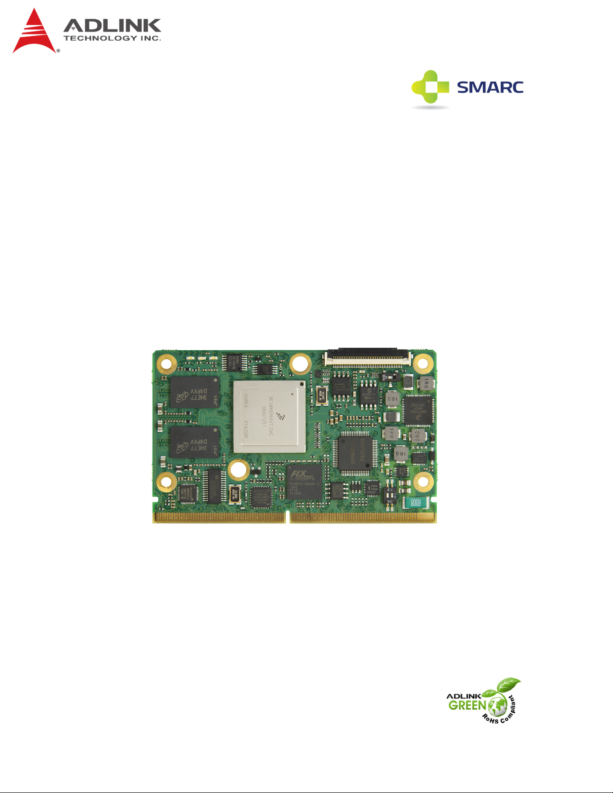
LEC‐iMX6
(Computer‐on‐Module)
Technical Reference
P/N50‐1Z167‐1000
Rev1.0
Advance Technologies. Automate the World.
Page 2
Disclaimer
Information in this document is provided in connection with ADLINK products. No license,
express or implied, by estoppel or otherwise, to any intellectual property rights is granted by
this document. Except as provided in ADLINK´s Terms and Conditions of Sale for such products, ADLINK assumes no liability whatsoever, and ADLINK disclaims any express or implied
warranty, relating to sale and/or use of ADLINK products including liability or warranties relating to fitness for a particular purpose, merchantability, or infringement of any patent, copyright or other intellectual property right. If you intend to use ADLINK products in or as medical
devices, you are solely responsible for all required regulatory compliance, including, without
limitation, Title 21 of the CFR (US), Directive 2007/47/EC (EU), and ISO 13485 & 14971, if
any. ADLINK may make changes to specifications and product descriptions at any time, without notice.
Trademarks
MS-DOS, Windows, Windows 95, Windows 98, Windows NT and Windows XP are trademarks
of Microsoft Corporation. PS/2 is a trademark of International Business Machines, Inc. Intel and
Solid State Drive are trademarks of Intel Corporation. PC/104 is a registered trademark of the
PC/104 Consortium. All other trademarks appearing in this document are the property of their
respective owners. CoreModule is a registered trademark, and ADLINK, Little Board, LittleBoard, MightyBoard, MightySystem, MilSystem, MiniModule, ReadyBoard, ReadyBox, ReadyPanel, RuffSystem, ReadySystem, and HPERC are trademarks of ADLINK Technology, Inc. All
other trademarks that may appear in this document or the ADLINK website are the properties of
their respective owners.
Revision History
Revision Reason for Change Date
1.0 Initial Release Nov/14
ADLINK Technology, Incorporated
www.adlinktech.com
© Copyright 2014 ADLINK Technology, Incorporated
Audience
This manual provides reference only for computer design engineers, including but not limited
to hardware and software designers and applications engineers. ADLINK Technology, Inc.
assumes you are qualified to design and implement prototype computer equipment.
ii
Page 3

LEC-iMX6
Table of Contents
1 Overview ........................................................................................................................... 1
1.1 Block Diagram........................................................................................................................ 1
1.2 Major Components (ICs)........................................................................................................ 2
1.3 Connectors, LEDs, and Switches .......................................................................................... 3
1.4 Specifications......................................................................................................................... 4
1.5 Getting Started....................................................................................................................... 7
2 Hardware ......................................................................................................................... 10
2.1 CPU ..................................................................................................................................... 10
2.2 Memory ............................................................................................................................... 10
2.3 eMMC NAND Flash ............................................................................................................. 10
3 Interfaces ........................................................................................................................ 11
3.1 Parallel LCD Video............................................................................................................... 11
3.2 18/24 Bit LVDS LCD ........................................................................................................... 11
3.3 HDMI (High-Definition Multimedia Interface) ....................................................................... 12
3.4 Camera PCAM..................................................................................................................... 12
3.5 Camera MIPI-CSI................................................................................................................. 12
3.6 PCIe ..................................................................................................................................... 12
3.7 Gigabit Ethernet .................................................................................................................. 12
3.8 USB 2.0 Ports ...................................................................................................................... 13
3.9 SATA.................................................................................................................................... 13
3.10 I2C ...................................................................................................................................... 13
3.11 SPI ....................................................................................................................................... 13
3.12 Serial (UART)....................................................................................................................... 14
3.13 SPDIF .................................................................................................................................. 14
3.14 I2S........................................................................................................................................ 14
3.15 CAN ..................................................................................................................................... 14
3.16 SD/SDIO Interface ............................................................................................................... 14
3.17 eMMC Interface ................................................................................................................... 15
3.18 GPIO .................................................................................................................................... 15
3.19 AFB Alternate Function Block .............................................................................................. 15
3.20 LPC Debug .......................................................................................................................... 15
4 Interface Signals............................................................................................................. 16
4.1 SMARC Interface ................................................................................................................. 16
4.2 Debug (DB40) ...................................................................................................................... 19
iii
Page 4

5 Power and System Management .................................................................................. 20
5.1 SEMA Utility ........................................................................................................................ 20
5.2 On-Board Power Supply ..................................................................................................... 20
5.3 System States ..................................................................................................................... 20
5.4 External Power Button ........................................................................................................ 20
5.5 Reset-In Signal.................................................................................................................... 20
5.6 External Battery................................................................................................................... 20
Appendix A Technical Support ........................................................................................ 21
iv
Page 5
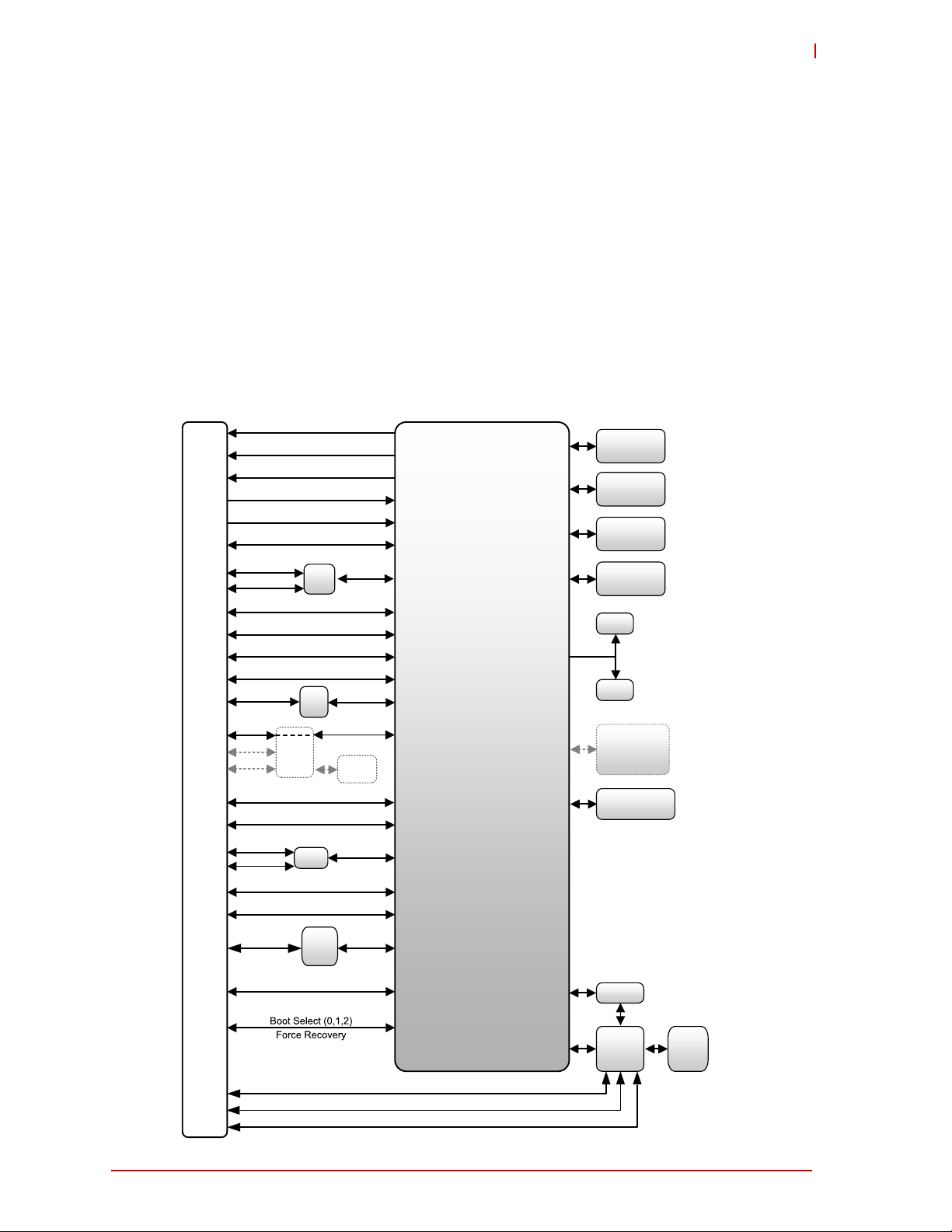
1 Overview
314-pin SMARC Connector
Freescale
iMX6
Memory
DDR3L
eMMC
(optional)
USB0 Host/OTG
LCD 24-bit RGB
eMMC/SDMMC (8-bit)
SDIO (4-bit)
40-pin Debug
Connector
PCAM (10-bit)
Memory
DDR3L
Memory
DDR3L
Memory
DDR3L
USB2 Host
USB1 Host
BMC
LM73
Thermal
Sensor
GbE
LAN
PHY
RGMII
SATA
1x I2C (option)
3x I2C
LVDS 24-bit (incl. DDC)
HDMI (Including DDC and CEC)
PCA
9535A
GPIO
12x GPIO
PCIe
switch
(option)
PCIe
PCIe
PCIe
PCIe
4x UARTS (2x 4, 2x 2)
2x CAN
MLB
SPDIF
MIPI CSI Camera, 2 lanes
MUX
I2S
SPI
SPI/I2S
1x SPI
SPI
Flash
(option)
RTC
Flash
Flash
1x SPI
1x I2C
USB
Hub
USB
Watchdog
LEC_iMX6_blk_diag_d
Power Management
This initial manual version presents a general overview of the LEC-iMX6. After reviewing this
document you should understand the following features of the LEC-iMX6.
Functional Block Diagram
Major Components (ICs) and Connectors (Locations and Descriptions)
Specifications
Boot Up Configuration
Interface Signal and Power Management Definitions
NOTE: Please refer to BSP readme documents in the Quick Drive for BSP installation instructions.
1.1 Block Diagram
Figure 1-1 represents the component functions of the module.
LEC-iMX6
Overview 1
Figure 1-1: Functional Block Diagram
Page 6
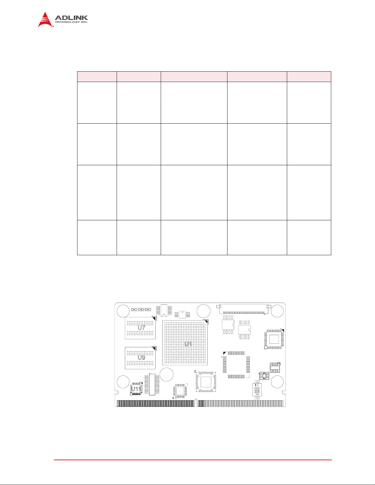
1.2 Major Components (ICs)
U7
U9
U1
Key:
U1 - CPU
U7 - DDR3L SDRAM
U9 - DDR3L SDRAM
U11 - Ethernet Controller
LEC_iMX6_Top_Comp_a
1 2
U11
Table 1-1 lists the major integrated circuits on the LEC-iMX6, including a brief description of
each IC. Figure 1-2 and Figure 1-3 show the locations of the major ICs.
Table 1-1: Major Integrated Circuit Descriptions and Functions
Chip Type Mfg. Model Description Function
CPU (U1) Freescale
Semiconductor
DDR3L
Micron MT41K256M16HA On-board DDR3L,
SDRAM (U7,
U8, U9, U10
[U8 and U10
on bottom
side])
Ethernet
Atheros AR8035-AL1B-R Integrated 10/100/
PHY
Transceiver
(U11)
eMMC,
Micron MTFC8GLDEA-4M-IT MultiMediaCard
NAND Flash
(U16 - on
bottom side)
i.MX 6Solo (one core)
i.MX 6Dual (two cores)
i.MX 6DualLite
(two cores, no SATA)
i.MX 6Quad (four cores)
800 MHz, ARM
Cortex-A8, 40nm SoC
(System on Chip)
1.35V, 4Gb,
32Mx16x8 System
Memory
1000 Mbps
single-port, tri-speed
Ethernet PHY
Transceiver
Controller and NAND
Flash Memory up to
64GB
Integrates
Processor
Core, Graphics
and Memory
Controller Hub,
and I/O Hub
Provides
high-speed
data transfer
Provides a
standard IEEE
802.3 Ethernet
interface for
Ethernet
transfer rates
up to 1000
Mbps
Provides
communication
and mass data
storage
capabilities
Figure 1-2: Component Locations (Top Side)
2 Overview
Page 7
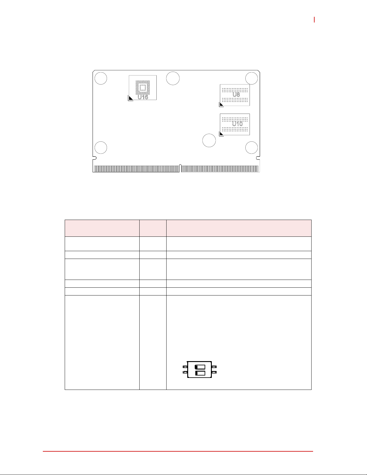
Figure 1-3: Component Locations (Bottom Side)
U8
U10
U16
LEC_iMX6_Bottom_Comp_a
Key:
U8 - DDR3L SDRAM
U10 - DDR3L SDRAM
U16 - eMMC, NAND Flash
ON
1 2
(1 2)
(4 3)
LEC-iMX6
1.3 Connectors, LEDs, and Switches
Table 1-2 describes the connectors, LEDs, and switches shown in Figure 1-4.
Table 1-2: Module Connector, LED, and Switch Descriptions
Connector, LED, Switch #
J1 – SMARC P-S Top/
CN2 Top 40-pin connector for debug card
LED1 Top Blue LED indicating system status activities for HW Reset,
LED2 Top Green LED for Power On
LED3 Top Red LED for Watchdog Activity
SW1 Top 4-pin dip switch for:
Board
Access
Bottom
Description
314-pin, MXM edge connector for Memory, Video, and I/O
functions.
SW Reset, Power Up, Power Down, Reset Button, Power
Button, and U-Boot_Select
• U-BOOT_SELECT: 1=off, 4=on [default]
1 = 8MB SPI Flash with U-BOOT+Debian
installer
4 = 4MB SPI Flash with U-BOOT
• WDT Disable: 2=off, 3=on [default]
Overview 3
Page 8
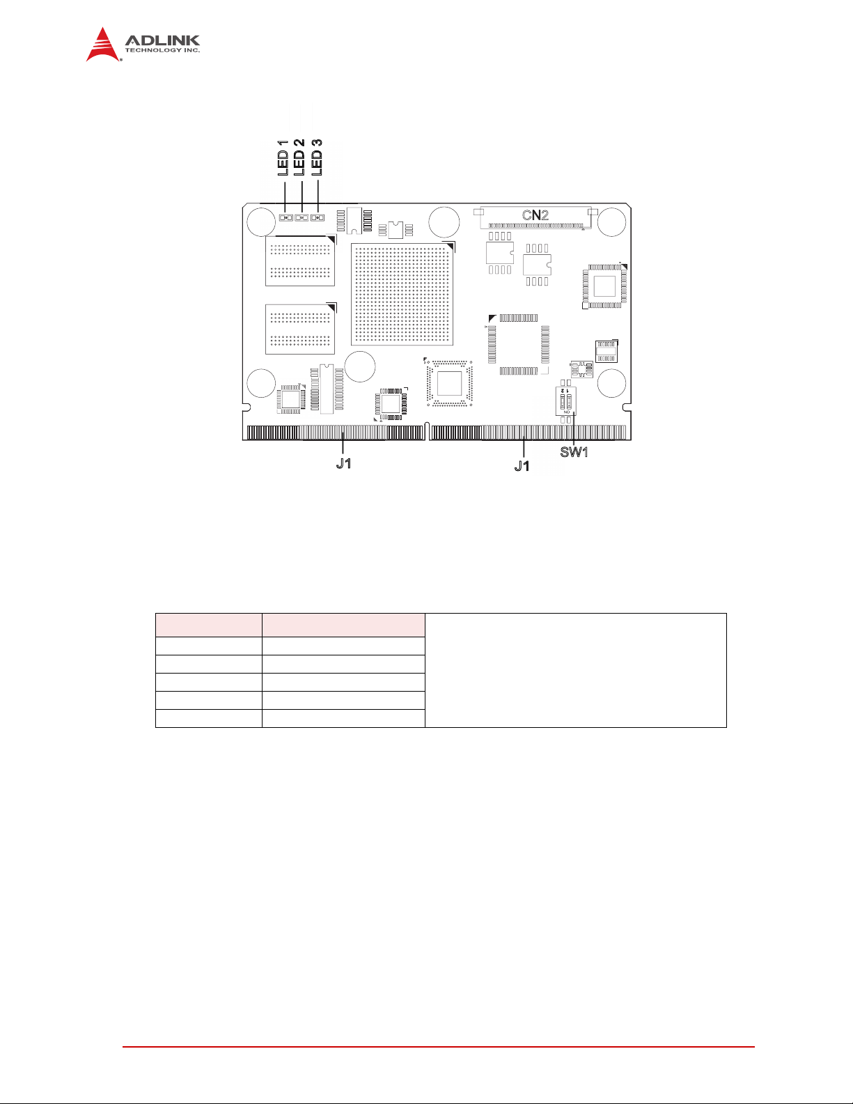
Figure 1-4: Connector, LED, and Switch Locations (Top Side)
LEC_iMX6_Top_Conn_a
1 2
Key:
J1 - SMARC Connector
CN2 - DB40 Debug Connector
LED1 - System Status, Blue
LED2 - Power On, Green
LED3 - Watchdog Activity, Red
SW1 - U-BOOT_Select
LED 1
LED 2
LED 3
1
J1
J1
J1
J1
1 2
SW1
CN2
1
1.4 Specifications
1.4.1 Physical Specifications
Table 1-3 lists the physical dimensions of the module.
Table 1-3: Weight and Footprint Dimensions
Item Dimension
Weight 0.02 kg (0.05 lb)
Height (overall) 3.05 mm (0.12 inches)
Board thickness 1.27 mm (0.05 inches)
Width 50.00 mm (1.97 inches)
Length 82.00 mm (3.23 inches)
Overall height is measured from the upper board
surface to the top of the highest permanent
component (CN2 connector) on the upper board
surface. This measurement does not include the
cooling solution, which can vary. The cooling
solution will probably increase this dimension.
4 Overview
Page 9
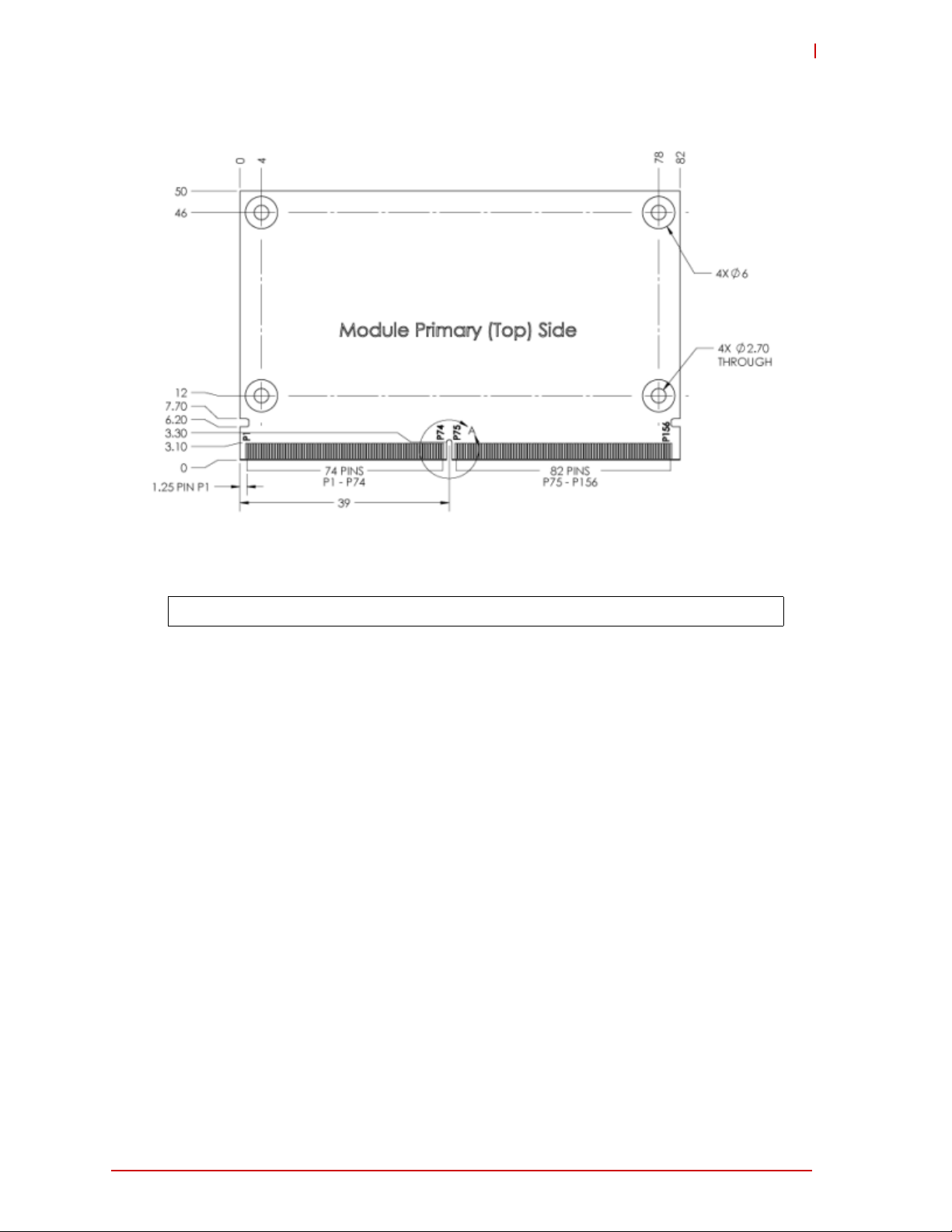
1.4.2 Mechanical Specifications
LEC-iMX6_mech_dmn_top_a
LEC-iMX6
Figure 1-5: Mechanical Dimensions (Top Side)
NOTE: All dimensions are given in millimeters.
Overview 5
Page 10

1.4.3 Power Specifications
Table 1-4 provides the power requirements for this module.
Table 1-4: Power Supply Requirements
Parameter
Input Type +3V to +5.25V Regulated DC voltage
In-rush Current @5V:
• Solo: 443mA
• Dual Lite: 456mA
• Dual: 794mA
• Quad: 813mA
Typical Idle Current @ 5V:
• Dual: 337mA
• Quad: 362mA
BIT (Burn-In Test) Current @5V:
Solo: 509mA
Dual Lite: 524mA
Dual: 902mA
Quad: 907mA
800MHz
Characteristics
Operating configurations:
In-rush operating configuration - Typical
Idle operating configuration - Typical
BIT operating configuration - Typical
1.4.4 Environmental Specifications
Table 1-5 provides the most efficient operating and storage condition ranges required for this
module.
Table 1-5: Environmental Requirements
Parameter Conditions
Temperature
Extended –40° to +85° C (–40° to +185° F)
Storage –55° to +85° C (–67° to +185° F)
Humidity
Operating 5% to 90% relative humidity, non-condensing
Non-operating 5% to 95% relative humidity, non-condensing
1.4.5 Thermal/Cooling Requirements
The LEC-iMX6 is designed to operate at its maximum CPU speed and requires a thermal solution. ADLINK offers one cooling option described in Table 1-6.
CAUTION: The optional heat spreader plate requires another form of cooling, such as a fan. A
heat spreader plate is not a complete thermal solution for the LEC-iMX6.
CAUTION: The overall system design must keep the ICs within their operating temperature
specifications.
Table 1-6: ADLINK Optional Cooling Option
Option Description
Heat Spreader Provides a simple thermal platform on which to build a cooling solution.
The heat spreader is available as an optional order item.
6 Overview
Page 11

LEC-iMX6
1.5 Getting Started
This section describes how to configure the boot select jumpers on the LEC-BASE baseboard
and how to configure U-Boot to run a Linux image.
1.5.1 Configure boot select jumpers
Before starting up the LEC-iMX6, the boot select jumpers on the LEC-BASE baseboard must be
configured to correspond with the storage location of the U-Boot boot loader. This section also
discusses boot requirements for the Operating System.
Before you boot your system, consider the storage locations of the following software:
U-Boot boot loader
Linux Operating System
The storage locations (devices) of these two software packages can be the same or distinct.
1. To boot the system from a specific boot device (location of the U-Boot boot loader), the
LEC-BASE boot select jumpers must be set as shown in the following photos.
Boot from module eMMC
(JP16=2-3; JP17=1-2; JP18 1-2; JP19=1-2)
Boot from carrier SATA disk
(JP16=2-3; JP17=2-3; JP18 2-3; JP19=1-2)
(JP16=1-2; JP17=1-2; JP18 1-2; JP19=1-2)
(JP16=1-2; JP17=2-3; JP18 2-3; JP19=1-2)
Boot from module SPI flash
Boot from carrier SD card
2. The storage location of the Operating System can be set during boot up through a
U-Boot command entry. Otherwise, the default setting will be used.
Overview 7
Page 12

1.5.2 Verify U-Boot Configuration
To ensure U-Boot will run a Linux image from the corresponding boot device, perform the following steps.
1. Make a serial connection between the COM1 port of the LEC-iMX6 target and a host
computer.
2. Open a terminal program with settings 115200 Baud, 8N1. The following screen
appears.
3. Press any key to interrupt and open the U-Boot command shell.
4. Enter pri at the U-Boot> command line to list all environmental variables set inside
U-Boot.
5. Find the appropriate variable and run the corresponding start command. For example:
run boot_usb.
8 Overview
Page 13

LEC-iMX6
6. To run Linux from USB by default, edit bootcmd using:
edit bootcmd
run boot_usb
save
Note: You need to enter “save” after making a change, or the new setting will be lost after the next boot.
Overview 9
Page 14

2 Hardware
2.1 CPU
The LEC-iMX6 product family offers four models of the Freescale™ i.MX6 CPU: the i.MX 6Solo
(1x Core), the i.MX 6Dual (2x Core), the i.MX 6DualLite (2x Core, single-display, no SATA), and
the i.MX 6Quad (4x Core). i.MX6 CPUs feature 64-bit/32-bit ARM Cortex-A9 processor cores
built on 40-nanometer process technology. The CPUs are designed for one-chip platforms, all
using the same package, and are pin compatible. Refer to the CPU data sheet and reference
manual at:
http://www.freescale.com/webapp/sps/site/taxonomy.jsp?code=IMX6X_SERIES.
2.2 Memory
The LEC-iMX6 employs one channel of 64-bit DDR3L on-board memory. Four SDRAM memory
chips provide up to 16Gb of non-ECC, unbuffered, low voltage system memory. Refer to the
SDRAM datasheet at:
http://www.micron.com/parts/dram/ddr3-sdram/mt41k256m16ha-125-it
2.3 eMMC NAND Flash
The module supports an optional on-board eMMC (Multi-Media Card) NAND chip with capacity
up to 64GB and can be used as the Boot device.The data signals are routed from the NAND
chip through the SDMMC pins on the SMARC connector. If the optional eMMC NAND chip is
present on the module, the eMMC interface will not be available for the baseboard on the
SMARC connector. Refer to the NAND Flash datasheet at:
http://www.micron.com/parts/nand-flash/managed-nand/mtfc8gldea-4m-it
10 Hardware
Page 15

3 Interfaces
This section provides descriptions of the interfaces and signals within the SMARC P-S (Primary-Secondary) connector.
Parallel LCD
LVDS
HDMI
Camera PCAM
Camera MIPI-CSI
PCIe
Gb Ethernet
USB 2.0 (Host and OTG)
SATA
I2C
SPI
Serial
SPDIF
I2S
CAN
SD/SDIO
eMMC
GPIO
AFB (Alternate Function Block; used for Media Local Bus [MLB])
Debug
The SMARC P-S connector provides the following features:
LEC-iMX6
NOTE: ADLINK Technology Inc. only supports the features/options tested and listed in this manual. The main chips used in the LEC-iMX6 may provide more features or options than are listed
for the LEC-iMX6, but some of these features or options are not supported on the module and
will not function as specified in the chip documentation.
3.1 Parallel LCD Video
The Parallel LCD interface on the LEC-iMX6 can be used in 18-Bit or 24-Bit modes at up to 225
Mpixels/sec.
The voltage level of the LCD interface is 1.8V.
The Parallel LCD interface uses the I2C2 interface from the i.MX 6. At the SMARC connector
the signal names are I2C_LCD_CK and I2C_LCD_DAT. The I2C interface is also shared
onboard with I2C_GP_CK and I2C_GP_DAT at the SMARC connector and with the PMIC I2C
interface.
3.2 18/24 Bit LVDS LCD
The module routes single-channel LVDS output from the CPU through the following SMARC
interface pins:
1 Clock pair (S134/S135)
4 Data pairs (S125/S126; S128/S129; S131/S132; S137/S138)
The LVDS port can support up to 165 Mpixels/sec and voltage levels of the LVDS specification.
Interfaces 11
Page 16

3.3 HDMI (High-Definition Multimedia Interface)
The HDMI port utilizes the following HDMI pins on the SMARC interface:
1 Clock pair (P101/P102)
3 Data pairs (P92/P93; P95/P96; P98/P99)
Service signals (P104-P107)
The HDMI interface is compliant with HDMI 1.4, HDMI CTS 1.4a, DVI 1.0 (with DVI-to-HDMI
adapter), and HDCP 1.4. The module supports CEC (Consumer Electronic Control) and Monitor
Detection for plug and unplug detection.
The voltage level of the HDMI interface complies with the HDMI 1.4 specification.
3.4 Camera PCAM
The Parallel Camera interface supports 10-Bit video with up to 240 MHz clock speed.
The voltage level of the PCAM interface is 1.8V.
3.5 Camera MIPI-CSI
The LEC-iMX6 brings out signals for an MIPI CSI-2 serial camera interface. This serial camera
port supports up to 1000 Mbps/lane in 1/2-lane mode.
The voltage level of the MIPI CSI-2 interface complies with the MIPI CSI specification.
3.6 PCIe
The module supports a PCIe port x1 lane, Gen 2.0 from the CPU, providing up to 5 Gb/s bandwidth in each direction. An optional PCIe switch IC allows for three lanes of PCIe expansion and
an optional SPI Flash. The i.MX 6 PCIe includes 3 Cores: Dual Mode core, Root Complex core,
and Endpoint core.
The LEC-iMX6 PCIe configurations include the following options:
1x PCIe 1x Gen 2.0
3x PCIe 1x Gen 2.0 using the optional PCIe switch
Service signals per lane:
PCIE_X_CKREQ# PCIE_X_RST# PCIE_X_PRSNT#
One PCIe wake-up input signal:
PCIE_WAKE# Input
3.7 Gigabit Ethernet
The LEC-iMX6 uses an Ethernet PHY, which is connected to the CPU Ethernet controller with
an RGMII interface. The PHY circuitry provides a standard IEEE 802.3 Ethernet interface for
1000BASE-T, 100BASE-TX, and 10BASE-Te applications. The following bullets highlight the
Ethernet interface:
Operates on TCP/IP, UDP/IP, and ICMP/IP protocol data or on IP header only
Supports IPv4 and IPv6
12 Interfaces
Page 17

LEC-iMX6
PCIe
Switch
SMARC Connector
DEBUG/Progr
CONNECTOR
I2C2
I2C1
PMIC
I2C
BMC
I2C3
Slave
Master
Master
Optional
I2C0
I2C1I2C2
Master
DDC
PMIC
I2C_PM
I2C_CAM
I2C_GP
I2C_LCD
HDMI_CTRL
R7
R3
R4
R5
R6
R2
R1
R8
GPIO Expander
HDMI DDC
NI
Slave
Slave
Optional
NI
Slave
Slave
Slave
Slave
Master
Master
Master
Slave
R9
RTC
Slave
Temp sens
Slave
iMX6
Processor
3.8 USB 2.0 Ports
The LEC-iMX6 provides two host USB ports and one OTG port. The two host ports are provided
from a 4-port USB HUB. All Ports are fully compliant with the USB 2.0 Specification.
3.9 SATA
Only the Dual and Quad variants of the LEC-iMX6 module provide a SATA interface. The SATA
interfaces on the Dual and Quad models comply with the following specifications.
Serial ATA 3.0
AHCI Revision 1.3
AMBA 2.0 from ARM
The interface supports 1.5Gb/s and 3.0Gb/s.
3.10 I2C
The CPU provides three I2C master ports, and the SMARC connector provides five I2C slave
ports for Camera, General Purpose, LCD, Power Management, and HDMI Control (private)
interfaces. Refer to the following block diagram. The I2C interfaces operate at data rates up to
400 kbps. All I2C interfaces have 1.8V pull ups with 1k resistors.
3.11 SPI
The LEC-iMX6 provides three SPI interfaces. SPI0 is multiplexed with I2S and connected to the
SMARC connector. SPI1 connects directly to the SMARC connector. The internal SPI interface
connects to the U-Boot flash memory devices.
The voltage levels of the SPI interfaces are 1.8V.
Interfaces 13
Page 18

3.12 Serial (UART)
The LEC-iMX6 provides four serial interfaces: Two ports are high-speed, 4-wire ports (with TX/
RX and RTS#/CTS#), and two ports are 2-wire (with TX/RX only.) Refer to the following table.
The voltage levels of the UART interfaces are 1.8V.
i.MX6 SMARC connector Bus width
UART1 SER0 4 wire bus
UART2 SER1 2 wire bus
UART5 SER2 4 wire bus
UART4 SER3 2 wire bus
3.13 SPDIF
The Sony/Philips Digital Interconnect Format (SPDIF) audio block is a stereo transceiver that
allows the processor to receive and transmit digital audio. Since the SPDIF internal data width is
24-bit, the eight most-significant bits of all registers return zeros. The SPDIF uses 2 wires, one
data output, and one input.
The voltage level of the SPDIF interface is 1.8V
3.14 I2S
The LEC-iMX6 provides one I2S audio interface, and the signals are brought out through the
I2S0 pins on the SMARC connector. The signals are shared with the SPI0 interface on the
SMARC connector. The signal that allows switching between SPI and I2S is GPIO1_IO3. The
default state is SPI (GPIO1_IO3 = low). When GPIO1_IO3 = high, I2S is switched through the
SMARC connector.
The voltage level of the I2S interface is 1.8V
3.15 CAN
The LEC-iMX6 provides two CAN (FLEXCAN) interfaces that comply with the CAN 2.0B protocol specification. Two CAN bus transceivers reside on the CPU and are not required on the
module. Refer to the following table for signal designators.
i.MX6 SMARC connector
FLEXCAN1 CAN0
FLEXCAN2 CAN1
The voltage level of the CAN interface is 1.8V
3.16 SD/SDIO Interface
Four parallel data lines comprise the SD/SDIO interface, supporting SD Card sockets. The
LEC-iMX6 provides a 4-bit transfer mode at the SMARC connector using the SDIO pins and the
SD2 interface of the i.MX 6 CPU. The following modes can be selected for data transfer:
SD/SDIO full speed mode (up to 25 MHz)
SD/SDIO high speed mode (up to 50 MHz)
SD/SDIO UHS-I mode (up to 208 MHz in SDR mode, up to 50 Mhz in DDR mode)
The SDIO interface can be selected as the Boot Device. The voltage level of the SD/SDIO interface is 3.3V
14 Interfaces
Page 19

LEC-iMX6
3.17 eMMC Interface
The LEC-iMX6 provides one eMMC NAND Flash memory chip with up to 64GB storage capacity, accessible from the baseboard and brought out from the CPU through the SDMMC pins on
the SMARC connector. The eMMC interface has an 8-bit width and complies with the MMC system specification.
3.18 GPIO
The LEC-iMX6 provides 12 GPIO signals. Seven signals (GPIO 4, 5, 6, 8, 9, 10, 11) are generated by the 9535A GPIO expander, and the remaining five signals (0, 1, 2, 3, and 7) originate
from the iMX6 CPU and are designated for CAM0 and CAM1 (PWR and RST). The GPIO signals can be utilized for General Purpose IOs as well as camera enable pins and camera field
input, as defined in the SMARC specification.
3.19 AFB Alternate Function Block
The AFB is used for an MLB (Media Local Bus) interface. The MLB is only supported in automotive and consumer parts.
3.20 LPC Debug
A 40-pin, front flip, DB40 connector allows access to debug and update the U-Boot boot loader,
BMC, and OS code on the module. (Refer to “Debug (DB40)” on page 19.)
Interfaces 15
Page 20

4 Interface Signals
4.1 SMARC Interface
Table 4-1 provides the pin signals for the SMARC P-S connector. Refer to the SMARC specification at http://www.sget.org/standards/smarc.html
Table 4-1: SMARC P-S Connector (J1) Signal Descriptions
Pin # Primary (Top Side) Pin # Secondary (Bottom Side)
P1 PCAM_PXL_CK1 S2 PCAM_HSYNC
P2 GND S3 GND
P3 CSI1_CK+/PCAM_D0 S4 PCAM_PXL_CK0
P4 CSI1_CK-/PCAM_D1 S5 I2C_CAM_CK
P5 PCAM_DE S6 CAM_MCK
P6 PCAM_MCK S7 I2C_CAM_DAT
P7 CSI1_D0+/PCAM_D2 S8 CSI0_CK+/PCAM_D10
P8 CSI1_D0-/PCAM_D3 S9 CSI0_CK-/PCAM_D11
P9 GND S10 GND
P10 CSI1_D1+/PCAM_D4 S11 CSI0_D0+/PCAM_D12
P11 CSI1_D1-/PCAM_D5 S12 CSI0_D0-/PCAM_D13
P12 GND S13 GND
P13 CSI1_D2+/PCAM_D6 S14 CSI0_D1+/PCAM_D14
P14 CSI1_D2-/PCAM_D7 S15 CSI0_D1-/PCAM_D15
P15 GND S16 GND
P16 CSI1_D3+/PCAM_D8 S17 Not connected
P17 CSI1_D3/PCAM_D9 S18 Not connected
P18 GND S19 Not connected
P19 GBE_MDI3- S20 Not connected
P20 GBE_MDI3+ S21 Not connected
P21 GBE_LINK100# (Ethernet Speed LED) S22 Not connected
P22 GBE_LINK1000# (Ethernet Speed LED) S23 Not connected
P23 GBE_MDI2- S24 Not connected
P24 GBE_MDI2+ S25 GND
P25 GBE_LINK_ACT# (LAN Link LED) S26 SDMMC_D0
P26 GBE_MDI1- S27 SDMMC_D1
P27 GBE_MDI1+ S28 SDMMC_D2
P28 GBE_CTREF S29 SDMMC_D3
P29 GBE0_MDI0- S30 SDMMC_D4
P30 GBE0_MDI0+ S31 SDMMC_D5
P31
P32
P33 SDIO_WP S34 GND
P34 SDIO_CMD S35 SDMMC_CK
P35 SDIO_CD# S36 SDMMC_CMD
P36 SDIO_CK S37 SDMMC_RST#
P37 SDIO_PWR_EN S38 AUDIO_MCK
P38 GND S39 I2S0_LRCK
P39 SDIO_D0 S40 I2S0_SDOUT
P40 SDIO_D1 S41 I2S0_SDIN
P41 SDIO_D2 S42 I2S0_CK
SPI0_CS1#
GND
for definitions of the SMARC signals.
S1 PCAM_VSYNC
S32 SDMMC_D6
S33 SDMMC_D7
16 Interface Signals
Page 21

Table 4-1: SMARC P-S Connector (J1) Signal Descriptions (Continued)
P42 SDIO_D3 S43 Not connected
P43 SPI0_CS0# S44 Not connected
P44 SPI0_CK S45 Not connected
P45 SPI0_DIN S46 Not connected
P46 SPI0_DO S47 GND
P47 GND S48 I2C_GP_CK
P48 SATA0_TX+ S49 I2C_GP_DAT
P49 SATA0_TX- S50 Not connected
P50 GND S51 Not connected
P51 SATA_RX+ S52 Not connected
P52 SATA_RX- S53 Not connected
P53 GND S54 Not connected
P54 SPI1_CS0# S55 Not connected
P55 SPI1_CS1# S56 Not connected
P56 SPI1_CK S57 Not connected
P57 SPI1_DIN S58 PCAM_ON_CSI1#
P58 SPI1_DO S59 SPDIF_OUT
P59 GND S60 SPDIF_IN
P60 USB0+ S61 GND
P61 USB0- S62 Not connected
P62 USB0_EN_OC# S63 Not connected
P63 USB0_VBUS_DET S64 GND
P64 USB0_OTG_ID S65 AFB_DIFF1+
P65 USB1+ S66 AFB_DIFF1P66
P67 USB1_EN_OC# S68 AFB_DIFF2+
P68 GND S69 AFB_DIFF2P69 USB2+ S70 GND
P70 USB2- S71 AFB_DIFF3+
P71 USB2_EN_OC# S72 AFB_DIFF3P72 PCIE_C_PRSNT# S73 GND
P73 PCIE_B_PRSNT# S74 AFB_DIFF4+
P74 PCIE_A_PRSNT# S75 AFB_DIFF4-
P75 PCIE_A_RST# S76 PCIE_B_RST#
P76 PCIE_C_CKREQ# S77 PCIE_C_RST#
P77 PCIE_B_CKREQ# S78 PCIE_C_RX+
P78 PCIE_A_CKREQ# S79 PCIE_C_RXP79 GND S80 GND
P80 PCIE_C_REFCK+ S81 PCIE_C_TX+
P81 PCIE_C_REFCK- S82 PCIE_C_TXP82 GND S83 GND
P83 PCIE_A_REFCK+ S84 PCIE_B_REFCK+
P84 PCIE_A_REFCK- S85 PCIE_B_REFCKP85 GND S86 GND
P86 PCIE_A_RX+ S87 PCIE_B_RX+
P87 PCIE_A_RX- S88 PCIE_B_RXP88 GND S89 GND
P89 PCIE_A_TX+ S90 PCIE_B_TX+
P90 PCIE_A_TX- P91 PCIE_B_TXP91 GND S92 GND
USB1-
Key Key
S67 GND
LEC-iMX6
Interface Signals 17
Page 22

Table 4-1: SMARC P-S Connector (J1) Signal Descriptions (Continued)
P92 HDMI_D2+ S93 LCD_D0
P93 HDMI_D2- S94 LCD_D1
P94 GND S95 LCD_D2
P95 HDMI_D1+ S96 LCD_D3
P96 HDMI_D1- S97 LCD_D4
P97 GND S98 LCD_D5
P98 HDMI_D0+ S99 LCD_D6
P99 HDMI_D0- S100 LCD_D7
P100 GND S101 GND
P101 HDMI_CK+ S102 LCD_D8
P102 HDMI_CK- S103 LCD_D9
P103 GND S104 LCD_D10
P104 HDMI_HPD S105 LCD_D11
P105 HDMI_CTRL_CK S106 LCD_D12
P106 HDMI_CTRL_DAT S107 LCD_D13
P107 HDMI_CEC S108 LCD_D14
P108 GPIO0 / CAM0_PWR# S109 LCD_D15
P109 GPIO1 / CAM1_PWR# S110 GND
P110 GPIO2 / CAM0_RST# S111 LCD_D16
P111 GPIO3 / CAM1_RST# S112 LCD_D17
P112 GPIO4 / HDA_RST# S113 LCD_D18
P113 GPIO5 / _PWM_OUT S114 LCD_D19
P114 GPIO6 / TACHIN S115 LCD_D20
P115 GPIO7 / PCAM_FLD S116 LCD_D21
P116 GPIO8 / CAN0_ERR# S117 LCD_D22
P117 GPIO9 / CAN1_ERR# S118 LCD_D23
P118 GPIO10 S119 GND
P119 GPIO11 S120 LCD_DE
P120 GND P121 LCD_VS
P121 I2C_PM_CK S122 LCD_HS
P122 I2C_PM_DAT S123 LCD_PCK
P123 BOOT_SEL0# S124 GND
P124 BOOT_SEL1# S125 LVDS0+
P125 BOOT_SEL2# S126 LVDS0P126 RESET_OUT# S127 LCD_BKLT_EN
P127 RESET_IN# S128 LVDS1+
P128 POWER_BTN# S129 LVDS1P129 SER0_TX S130 GND
P130 SER0_RX S131 LVDS2+
P131 SER0_RTS# S132 LVDS2P132 SER0_CTS# S133 LCD_VDD_EN
P133 GND S134 LVDS_CK+
P134 SER1_TX S135 LVDS_CKP135 SER1_RX S136 GND
P136 SER2_TX S137 LVDS3+
P137 SER2_RX S138 LVDS3P138 SER2_RTS# S139 I2C_LCD_CK
P139 SER2_CTS# S140 I2C_LCD_DAT
P140 SER3_TX S141 LCD_BKLT_PWM
P141 SER3_RX S142 Not connected
P142 GND S143 GND
18 Interface Signals
Page 23

LEC-iMX6
Table 4-1: SMARC P-S Connector (J1) Signal Descriptions (Continued)
P143 CAN0_TX S144 Not connected
P144 CAN0_RX S145 WDT_TIME_OUT#
P145 CAN1_TX S146 PCIE_WAKE
P146 CAN1_RX S147 VDD_RTC
P147 VDD_IN S148 LID#
P148 VDD_IN S149 SLEEP#
P149 VDD_IN S150 VIN_PWR_BAD#
P150 VDD_IN S151 CHARGING#
P151 VDD_IN S152 CHARGER_PRSNT#
P152 VDD_IN S153 CHARGER_STBY#
P153 VDD_IN S154 CARRIER_PWR_ON
P154 VDD_IN S155 FORCE_RECOV#
P155 VDD_IN S156 BATLOW#
P156 VDD_IN S157 TEST#
S158 VDD_IO_SEL#
4.2 Debug (DB40)
Table 4-2 lists the pin signals of the CN2 connector, which provides 40 pins, 1 row, consecutive
sequence with 0.02" (0.50mm) pitch.
Table 4-2: Debug Interface Signals (CN2)
Pin # Signal Interface
1 RESVD
2 SMC_STATUS SMC Debug
3 Not Connected SMC Debug
4 SEL_U-BOOT SMC Debug
5 POSTWDT_DIS# SMC Debug
6 SUS_S5# Test Point
7 SUS_S4# Test Point
8 SUS_S3# Test Point
9 CB_PWROK Test Point
10 CB_RESET# Test Point
11 SYS_RESET# Test Point
12 PWRBTN# Test Point
13 SMC_OCD0B SMC Program
14 SMC_OCD0A SMC Program
15 SMC_CLK SMC Program
16 SMC_DATA SMC Program
17 SMC_RESET_IN# SMC Program
18 SMC_FLMD0 SMC Program
19 SMC_RXD6 SMC Program
20 SMC_TXD6 SMC Program
21
22 3V3_DUAL SMC Program
23 3V3_SMC1 SMC Program
24 Not Connected
25 Not Connected
26 LPC_AD2 LPC Debug Card
27 LPC_AD3 LPC Debug Card
28 LPC_FRAME# LPC Debug Card
29 CLK33_LPC LPC Debug Card
GND
Interface Signals 19
Page 24

Table 4-2: Debug Interface Signals (CN2) (Continued)
30 RST# LPC Debug Card
31 Not Connected
32 Not Connected
33 LPC_3V3 LPC Debug Card
34 SPI_U-BOOT_CLK SPI Program
35 SPI_U-BOOT_MOSI SPI Program
36 SPI_U-BOOT_MISO SPI Program
37 SPI_U-BOOT_CS1# SPI Program
38 SPI_U-BOOT_CS0# SPI Program
39
40 VCC_SPI_IN SPI Program
NOTE: The gray table cells denote ground.
GND
5 Power and System Management
5.1 SEMA Utility
Under the management of the BMC chip (Board Management Controller), the SEMA utility
(Smart Embedded Management Agent) provides system control and failure protection—counting, monitoring, and measuring hardware and software events, from which the SOC can trigger
corrective commands. The optional SEMA Cloud utility not only controls local events on the
module but system client events on the IoT.
5.2 On-Board Power Supply
The on-board power supply generates all necessary voltages from the single supply voltage
range of 3V to 5.25V DC.
Externally, +5V Standby can be used instead of the on-board generated +5V Standby voltage.
5.3 System States
The following system states are supported: Suspend to RAM, Freeze, and Standby.
5.4 External Power Button
The board provides support for a power button to initiate transition from Off to On and On to Off
(hold for 4 seconds to power off.)
5.5 Reset-In Signal
The board provides support for a reset button to restart the system.
5.6 External Battery
The module supports an external RTC that is powered by a battery on the baseboard.
20 Power and System Management
Page 25

Appendix A Technical Support
Contact us should you require any service or assistance.
ADLINK Technology, Inc.
Address: 9F, No.166 Jian Yi Road, Zhonghe District
New Taipei City 235, Taiwan
ᄅקؑխࡉ৬ԫሁ 166 ᇆ 9 ᑔ
Tel: +886-2-8226-5877
Fax: +886-2-8226-5717
Email: service@adlinktech.com
Ampro ADLINK Technology, Inc.
Address: 5215 Hellyer Avenue, #110, San Jose, CA 95138, USA
Tel: +1-408-360-0200
Toll Free: +1-800-966-5200 (USA only)
Fax: +1-408-360-0222
Email: info@adlinktech.com
ADLINK Technology (China) Co., Ltd.
Address: Ϟ⍋Ꮦ⌺ϰᮄᓴ∳催⾥ᡔು㢇䏃 300 ো(201203)
300 Fang Chun Rd., Zhangjiang Hi-Tech Park,
Pudong New Area, Shanghai, 201203 China
Tel: +86-21-5132-8988
Fax: +86-21-5132-3588
Email: market@adlinktech.com
ADLINK Technology, Inc. provides a number of methods for contacting Technical Support listed
in Table A-1 below. Requests for support through Ask an Expert are given the highest priorities,
and usually will be addressed within one working day.
ADLINK Ask an Expert – This is a comprehensive support center designed to meet all
your technical needs. This service is free and available 24 hours a day through the
ADLINK web site at http://www.adlinktech.com/AAE/
base of Frequently Asked Questions, which will help you with the common information
requested by most customers. This is a good source of information to look at first for your
technical solutions. However, you must register online if you wish to use the Ask a Question feature.
ADLINK strongly suggests that you register with the web site. By creating a profile on the
ADLINK web site, you will have a portal page called “My ADLINK”, unique to you with
access to exclusive services and account information.
Personal Assistance – You may also request personal assistance by creating an Ask an
Expert account and then going to the Ask a Question feature. Requests can be submitted 24 hours a day, 7 days a week. You will receive immediate confirmation that your
request has been entered. Once you have submitted your request, you must log in to go
to the My Question area where you can check status, update your request, and access
other features.
Download Service – This service is also free and available 24 hours a day at
http://www.adlinktech.com
. For certain downloads such as technical documents and soft-
ware, you must register online before you can log in to this service.
. This includes a searchable data-
LEC-iMX6
Table A-1: Technical Support Contact Information
Method Contact Information
Ask an Expert http://www.adlinktech.com/AAE/
Web Site http://www.adlinktech.com
Standard Mail
21
Page 26

Table A-1: Technical Support Contact Information (Continued)
ADLINK Technology, Inc. (French Liaison Office)
Address: 6 allée de Londres, Immeuble Ceylan
91940 Les Ulis, France
Tel: +33 (0) 1 60 12 35 66
Fax: +33 (0) 1 60 12 35 66
Email: france@adlinktech.com
ADLINK Technology Japan Corporation
Address: ͱ101-0045 ᵅҀ䛑ҷ⬄⼲⬄䤯ފ⬎ 3-7-4
⼲⬄ 374 ɛɳ 4F
KANDA374 Bldg. 4F, 3-7-4 Kanda Kajicho,
Chiyoda-ku, Tokyo 101-0045, Japan
Tel: +81-3-4455-3722
Fax: +81-3-5209-6013
Email: japan@adlinktech.com
ADLINK Technology, Inc. (Korean Liaison Office)
Address: 137-881 昢殾柢 昢爎割 昢爎堆嵢 326, 802 (昢爎壟, 微汾瘶捒娯)
802, Mointer B/D, 326 Seocho-daero, Seocho-Gu,
Seoul 137-881, Korea
Tel: +82-2-2057-0565
Fax: +82-2-2057-0563
Email: korea@adlinktech.com
ADLINK Technology Singapore Pte. Ltd.
Address: 84 Genting Lane #07-02A, Cityneon Design Centre
Singapore 349584
Tel: +65-6844-2261
Fax: +65-6844-2263
Email: singapore@adlinktech.com
ADLINK Technology Singapore Pte. Ltd. (Indian Liaison Office)
Address: #50-56, First Floor, Spearhead Towers
Margosa Main Road (between 16th/17th Cross)
Malleswaram, Bangalore - 560 055, India
Tel: +91-80-65605817, +91-80-42246107
Fax: +91-80-23464606
Email: india@adlinktech.com
ADLINK Technology Beijing
Address: ࣫ҀᏖ⍋⎔Ϟഄϰ䏃 1 োⲜ߯ࡼ E ᑻ 801 ᅸ(100085)
Rm. 801, Power Creative E, No. 1 Shang Di East Rd.
Beijing, 100085 China
Tel: +86-10-5885-8666
Fax: +86-10-5885-8626
Email: market@adlinktech.com
ADLINK Technology Shenzhen
Address: ⏅ഇᏖቅ⾥ᡔು催ᮄϗ䘧᭄ᄫᡔᴃು
A1 2 ὐ C (518057)
2F, C Block, Bldg. A1, Cyber-Tech Zone, Gao Xin Ave. Sec. 7
High-Tech Industrial Park S., Shenzhen, 518054 China
Tel: +86-755-2643-4858
Fax: +86-755-2664-6353
Email: market@adlinktech.com
LiPPERT ADLINK Technology GmbH
Address: Hans-Thoma-Strasse 11, D-68163
Mannheim, Germany
Tel: +49-621-43214-0
Fax: +49-621 43214-30
Email: emea@adlinktech.com
22
Page 27

Table A-1: Technical Support Contact Information (Continued)
ADLINK Technology, Inc. (Israeli Liaison Office)
Address: 27 Maskit St., Corex Building
PO Box 12777
Herzliya 4673300, Israel
Tel: +972-54-632-5251
Fax: +972-77-208-0230
Email: israel@adlinktech.com
ADLINK Technology, Inc. (UK Liaison Office)
Tel: +44 774 010 59 65
Email: UK@adlinktech.com
LEC-iMX6
23
Page 28

24
 Loading...