

Page 1
LEC‐3517
(Computer‐on‐Module)
Technical Reference
P/N50‐1Z152‐1000
Advance Technologies. Automate the World.
Page 2
Disclaimer
Information in this document is provided in connection with ADLINK products. No license,
express or implied, by estoppel or otherwise, to any intellectual property rights is granted by this
document. Except as provided in ADLINK´s Terms and Conditions of Sale for such products,
ADLINK assumes no liability whatsoever, and ADLINK disclaims any express or implied warranty, relating to sale and/or use of ADLINK products including liability or warranties relating to
fitness for a particular purpose, merchantability, or infringement of any patent, copyright or other
intellectual property right. If you intend to use ADLINK products in or as medical devices, you
are solely responsible for all required regulatory compliance, including, without limitation, Title
21 of the CFR (US), Directive 2007/47/EC (EU), and ISO 13485 & 14971, if any. ADLINK may
make changes to specifications and product descriptions at any time, without notice.
Trademarks
CoreModule is a registered trademark, and ADLINK, Little Board, LittleBoard, MightyBoard,
MightySystem, MilSystem, MiniModule, ReadyBoard, ReadyBox, ReadyPanel, RuffSystem,
and ReadySystem are trademarks of ADLINK Technology, Inc. All other marks are the property of their respective companies.
Revision History
Revision Reason for Change Date
1000 Initial Release Dec/13
ADLINK Technology, Incorporated
5215 Hellyer Avenue, #110
San Jose, CA 95138-1007
Tel. 408 360-0200
Fax 408 360-0222
www.adlinktech.com
© Copyright 2013 ADLINK Technology, Incorporated
Audience
This manual provides reference only for computer design engineers, including but not limited
to hardware and software designers and applications engineers. ADLINK Technology, Inc.
assumes you are qualified to design and implement prototype computer equipment.
ii
Page 3

LEC-3517
Table of Contents
1 Overview ........................................................................................................................... 1
1.1 Block Diagram........................................................................................................................ 1
1.2 Major Components (ICs)........................................................................................................ 2
1.3 Connectors............................................................................................................................. 3
1.4 Specifications......................................................................................................................... 3
1.5 Interface Signals .................................................................................................................... 5
Appendix A Technical Support ......................................................................................... 11
iii
Page 4

iv
Page 5
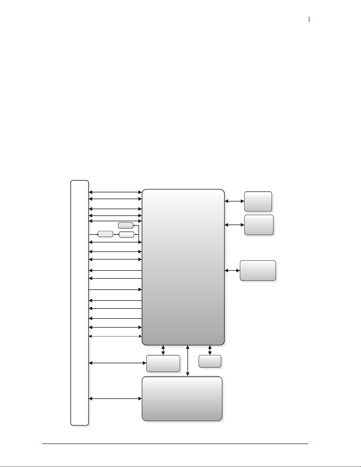
1 Overview
314-pin SMARC Connector
Texas Instruments
Micro Processor
®
AM3517
Texas Instruments
®
PMIC
(Power Management IC)
TPS650732
Memory
1Gb DDR2
64x16
NAND
4Gb (8-bit)
Memory
1Gb DDR2
64x16
USB1 Host
USB0 Host/OTG
4x UART (2x 4-pin, 2x 2-pin)
LCD 24-bit RGB
LAN PHY
SMSC LAN8710A-EZK
10/100 Mbps
Power
1x CAN
SPI0 / SPI1
I2S (3x)
I2C (3x)
GPIO (12x)
SDMMC (8-bit)
SDIO (4-bit)
10-pin JTAG
connector
Watchdog
Management
Camera (8-bit) +I2C
LCD Support + I2C
Boot Select (0,1,2)
Force Recovery
LEC_3517_Blk_Diag_a
EEPROM
Level
Shift
RTC
VRTC
This initial manual version presents a general overview of the LEC-3517 Computer-On-Module
(COM). The next version of this manual shall include more detailed information including user
interface descriptions, boot setup access and menu settings, memory map, interrupt channel
assignments, and I/O address map. After reviewing this document you should understand the
following features of the LEC-3517.
Functional Block Diagram
Major Component (IC) Locations and Descriptions
Connector Location and Description
Specifications
SMARC Interface Signal Definitions
NOTE: Please refer to BSP readme documents in the Quick Drive for BSP installation instructions.
1.1 Block Diagram
Figure 1-1 represents the component functions of the module.
LEC-3517
Figure 1-1: Functional Block Diagram
Overview 1
Page 6
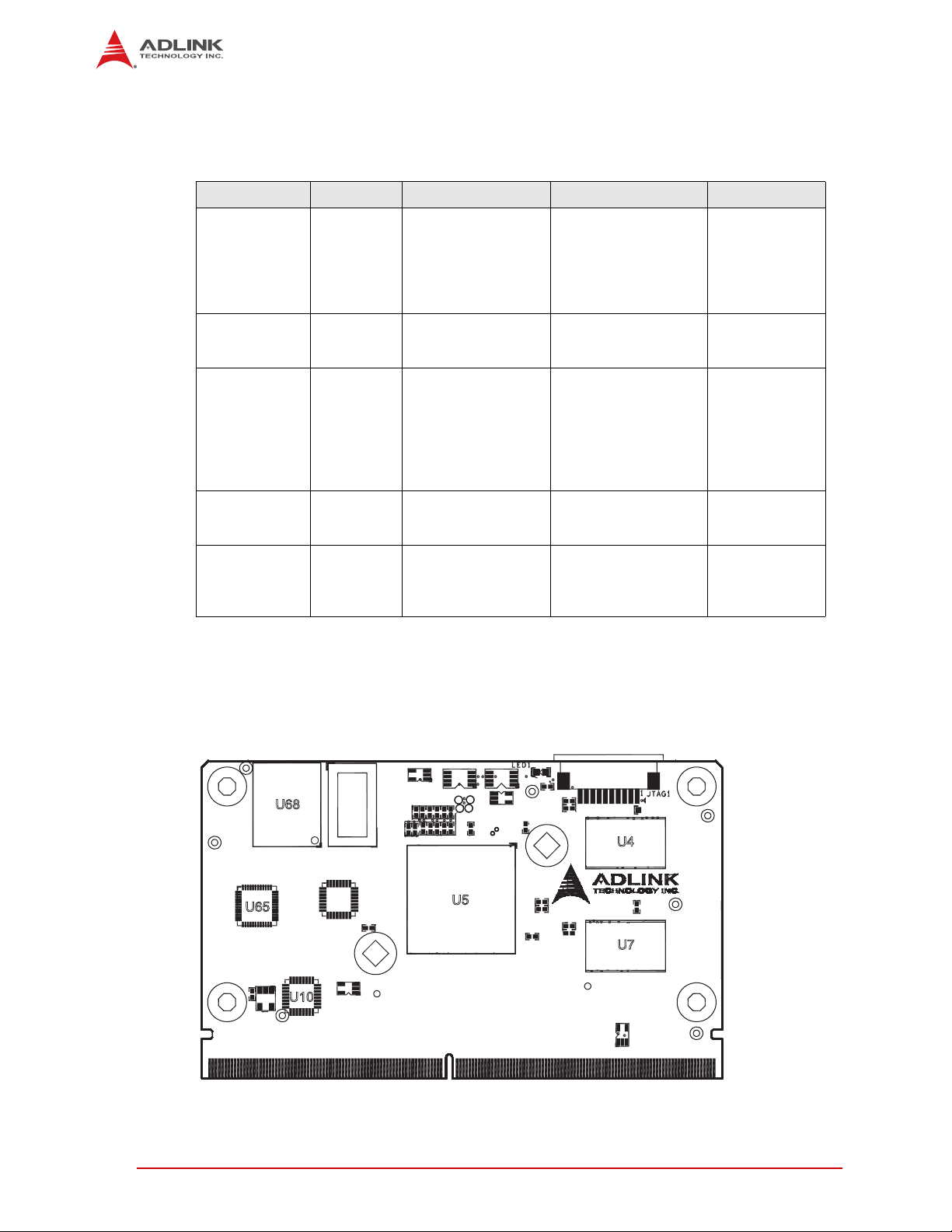
1.2 Major Components (ICs)
U68
U65
U10
U5
U7
U4
Key:
U4, U7 - DDR2 SDRAM
U5 - CPU
U10 - Ethernet Transceiver
U65 - Power Management IC
U68 - NAND Flash Staorage
LEC_3517_Top_Comp_a
Table 1-1 lists the major integrated circuits on the LEC-3517, including a brief description of
each IC. Figure 1-2 shows the locations of the major ICs.
Table 1-1: Major Integrated Circuit Descriptions and Functions
Chip Type Mfg. Model Description Function
CPU (U5) Texas
Instruments
DDR2 SDRAM
Hynix H5PS1G63JFR-SGC On-board DDR2, 1Gb,
(U4, U7)
Ethernet
SMSC LAN8710AI-EXK-TR Single-port, Fast
Transceiver
(U10)
PMIC (U65) Texas
Instruments
NAND Flash
Micron MT29F4G16ABBDA
(U68)
AM3517 ARM
Cortex-A8
600MHz
Microprocessor
64Mx16 System
Memory
Ethernet PHY
Transceiver
TP650732RSLR Single-chip, power
management solution
Rugged, Solid State
H4-IT
Storage
Integrates
Processor Core,
Graphics and
Memory
Controller Hub,
and I/O Hub
Provides
high-speed data
transfer
Provides a
standard IEEE
802.3 Ethernet
interface for
Ethernet
transfer rates up
to 100 Mb/s
Provides power
path
management
Provides 4Gb,
8-bit data
storage and
transfer
2 Overview
Figure 1-2: Component Locations (Top Side)
Page 7

1.3 Connectors
J1
LEC_3517_Top_Conn_a
Key:
J1 - SMARC Connector
Table 1-2 describes the connectors shown in Figure 1-3.
Table 1-2: Module Connector Description
Connector#
J1 – SMARC P-S Top/
JTAG1 Top 10-pin connector for debugging
LED1 Top Green LED for Power On
Board
Access
Bottom
314-pin, MXM edge connector for Memory, Video, and I/O
functions.
LEC-3517
Description
1.4 Specifications
Physical Specifications
Table 1-3 lists the physical dimensions of the module.
Weight 0.02 kg (0.05 lb)
Height (overall) 3.05 mm (0.12 inches)
Board thickness 1.27 mm (0.05 inches)
Width 50.00 mm (1.97 inches)
Length 82.00 mm (3.23 inches)
Overview 3
Figure 1-3: Connector Location (Top Side)
Table 1-3: Weight and Footprint Dimensions
Item Dimension
Overall height is measured from the upper board
surface to the top of the highest permanent
component (JTAG1 connector) on the upper board
surface. This measurement does not include the
cooling solution, which can vary. The cooling
solution will probably increase this dimension.
Page 8

Mechanical Specifications
J1
1.54 (39.00mm)
3.07 (78.00mm)
3.16 (80.30mm)
3.23 (82.0mm)
2.14 (54.39mm)
1.08 (27.39mm)
0.16 (4.00mm)
0.00
0.00
1.97 (50.00mm)
1.81 (46.00mm)
0.47 (12.00mm)
0.30 (7.70mm)
0.24 (6.20mm)
0.78 (19.69mm)
1.44 (36.69mm)
LEC_3517_Top_Dmn_a
Figure 1-4: Mechanical Dimensions (Top Side)
All dimensions are given in inches and millimeters.
Power Specifications
Table 1-4 provides the power requirements for this module.
Table 1-4: Power Supply Requirements
Parameter
Input Type Regulated DC voltage
In-rush
Voltage & Current
Typical Idle
Voltage & Current
BIT*
Voltage & Current
Operating configurations:
In-rush operating configuration - To be determined
Idle operating configuration - To be determined
*BIT = Burn-In-Test operating configuration - To be determined
Not yet measured
Not yet measured
Not yet measured
600Mhz
Characteristics
4 Overview
Page 9

LEC-3517
Environmental Specifications
Table 1-5 provides the most efficient operating and storage condition ranges required for this
module.
Table 1-5: Environmental Requirements
Parameter Conditions
Temperature
Standard –20° to +70° C (-4° to +158° F)
Extended (Optional) –40° to +85° C (–40° to +185° F)
Storage –55° to +85° C (–67° to +185° F)
Humidity
Operating 5% to 90% relative humidity, non-condensing
Non-operating 5% to 95% relative humidity, non-condensing
Thermal/Cooling Requirements
The LEC-3517 is designed to operate at its maximum CPU speed and requires a thermal solution. ADLINK offers one optional thermal solution described in Table 1-6.
The overall system design must keep the ICs within their operating temperature
specifications.
Table 1-6: ADLINK Optional Cooling Solutions
Cooling Solution Description
Passive Heatsink
(without fan)
Qualified to maintain optimal performance up to +85°C. (See Quick Start
Guide for P/N of heatsink.)
1.5 Interface Signals
Table 1-7 provides the pin signals for the SMARC P-S connector. Refer to the SMARC specification at http://www.sget.org/standards/smarc.html
Table 1-7: SMARC P-S Connector Signal Descriptions
Pin # Primary (Top Side) Pin # Secondary (Bottom Side)
P1 Not connected S2 PCAM_HSYNC
P2 GND S3 GND
P3 CSI1_CK+/PCAM_D0 S4 PCAM_PXL_CK0
P4 CSI1_CK-/PCAM_D1 S5 I2C_CAM_CK
P5 Not connected S6 CAM_MCK
P6 PCAM_MCK S7 I2C_CAM_DAT
P7 CSI1_D0+/PCAM_D2 S8 Not connected
P8 CSI1_D0-/PCAM_D3 S9 Not connected
P9 GND S10 GND
P10 CSI1_D1+/PCAM_D4 S11 Not connected
P11 CSI1_D1-/PCAM_D5 S12 Not connected
P12 GND S13 GND
P13 CSI1_D2+/PCAM_D6 S14 Not connected
P14 CSI1_D2-/PCAM_D7 S15 Not connected
P15 GND S16 GND
P16 Not connected S17 Not connected
P17 Not connected S18 Not connected
P18 GND S19 Not connected
for definitions of the SMARC signals.
S1 PCAM_VSYNC
Overview 5
Page 10

Table 1-7: SMARC P-S Connector Signal Descriptions (Continued)
P19 Not connected S20 Not connected
P20 Not connected S21 Not connected
P21 GBE_LINK100# (Ethernet Speed
LED)
P22 Not connected S23 Not connected
P23 Not connected S24 Not connected
P24 Not connected S25 GND
P25 GBE_LINK_ACT# (LAN Link LED) S26 SDMMC_D0
P26 GBE_MDI1- S27 SDMMC_D1
P27 GBE_MDI1+ S28 SDMMC_D2
P28 GBE_CTREF S29 SDMMC_D3
P29 GBE0_MDI0- S30 SDMMC_D4
P30 GBE0_MDI0+ S31 SDMMC_D5
P31
P32
P33 SDIO_WP S34 GND
P34 SDIO_CMD S35 SDMMC_CK
P35 SDIO_CD# S36 SDMMC_CMD
P36 SDIO_CK S37 SDMMC_RST#
P37 SDIO_PWR_EN S38 Not connected
P38 GND S39 I2S0_LRCK
P39 SDIO_D0 S40 I2S0_SDOUT
P40 SDIO_D1 S41 I2S0_SDIN
P41 SDIO_D2 S42 I2S0_CK
P42 SDIO_D3 S43 I2S1_LRCK
P43 SPI0_CS0# S44 I2S1_SDOUT
P44 SPI0_CK S45 I2S1_SDIN
P45 SPI0_DIN S46 I2S1_CK
P46 SPI0_DO S47 GND
P47 GND S48 I2C_GP_CK
P48 Not connected S49 I2C_GP_DAT
P49 Not connected S50 I2S2_LRCK
P50 GND S51 I2S2_SDOUT
P51 Not connected S52 I2S2_SDIN
P52 Not connected S53 I2S2_CK
P53 GND S54 Not connected
P54 SPI1_CS0# S55 Not connected
P55 SPI1_CS1# S56 Not connected
P56 SPI1_CK S57 PCAM_ON_CSI0#
P57 SPI1_DIN S58 PCAM_ON_CSI1#
P58 SPI1_DO S59 Not connected
P59 GND S60 Not connected
P60 USB0+ S61 GND
P61 USB0- S62 Not connected
P62 USB0_EN_OC# S63 Not connected
P63 USB0_VBUS_DET S64 GND
P64 USB0_OTG_ID S65 Not connected
P65 USB1+ S66 Not connected
P66
P67 USB1_EN_OC# S68 Not connected
P68 GND S69 Not connected
SPI0_CS1#
GND
USB1-
S22 Not connected
S32 SDMMC_D6
S33 SDMMC_D7
S67 GND
6 Overview
Page 11

Table 1-7: SMARC P-S Connector Signal Descriptions (Continued)
P69 Not connected S70 GND
P70 Not connected S71 Not connected
P71 USB2_EN_OC# S72 Not connected
P72 Not connected S73 GND
P73 Not connected S74 Not connected
P74 Not connected S75 Not connected
Key Key
P75 Not connected S76 Not connected
P76 Not connected S77 Not connected
P77 Not connected S78 Not connected
P78 Not connected S79 Not connected
P79 GND S80 GND
P80 Not connected S81 Not connected
P81 Not connected S82 Not connected
P82 GND S83 GND
P83 Not connected S84 Not connected
P84 Not connected S85 Not connected
P85 GND S86 GND
P86 Not connected S87 Not connected
P87 Not connected S88 Not connected
P88 GND S89 GND
P89 Not connected S90 Not connected
P90 Not connected P91 Not connected
P91 GND S92 GND
P92 Not connected S93 LCD_D0
P93 Not connected S94 LCD_D1
P94 GND S95 LCD_D2
P95 Not connected S96 LCD_D3
P96 Not connected S97 LCD_D4
P97 GND S98 LCD_D5
P98 Not connected S99 LCD_D6
P99 Not connected S100 LCD_D7
P100 GND S101 GND
P101 Not connected S102 LCD_D8
P102 Not connected S103 LCD_D9
P103 GND S104 LCD_D10
P104 Not connected S105 LCD_D11
P105 Not connected S106 LCD_D12
P106 Not connected S107 LCD_D13
P107 Not connected S108 LCD_D14
P108 GPIO0 / CAM0_PWR# S109 LCD_D15
P109 GPIO1 / CAM1_PWR# S110 GND
P110 GPIO2 / CAM0_RST# S111 LCD_D16
P111 GPIO3 / CAM1_RST# S112 LCD_D17
P112 GPIO4 / HDA_RST# S113 LCD_D18
P113 GPIO5 / _PWM_OUT S114 LCD_D19
P114 GPIO6 / TACHIN S115 LCD_D20
P115 GPIO7 / PCAM_FLD S116 LCD_D21
P116 GPIO8 / CAN0_ERR# S117 LCD_D22
P117 GPIO9 / CAN1_ERR# S118 LCD_D23
P118 GPIO10 S119 GND
LEC-3517
Overview 7
Page 12

Table 1-7: SMARC P-S Connector Signal Descriptions (Continued)
P119 GPIO11 S120 LCD_DE
P120 GND P121 LCD_VS
P121 I2C_PM_CK S122 LCD_HS
P122 I2C_PM_DAT S123 LCD_PCK
P123 BOOT_SEL0# S124 GND
P124 BOOT_SEL1# S125 Not connected
P125 BOOT_SEL2# S126 Not connected
P126 RESET_OUT# S127 LCD_BKLT_EN
P127 RESET_IN# S128 Not connected
P128 POWER_BTN# S129 Not connected
P129 SER0_TX S130 GND
P130 SER0_RX S131 Not connected
P131 SER0_RTS# S132 Not connected
P132 SER0_CTS# S133 LCD_VDD_EN
P133 GND S134 Not connected
P134 SER1_TX S135 Not connected
P135 SER1_RX S136 GND
P136 SER2_TX S137 Not connected
P137 SER2_RX S138 Not connected
P138 SER2_RTS# S139 I2C_LCD_CK
P139 SER2_CTS# S140 I2C_LCD_DAT
P140 SER3_TX S141 LCD_BKLT_PWM
P141 SER3_RX S142 Not connected
P142 GND S143 GND
P143 CAN0_TX S144 Not connected
P144 CAN0_RX S145 WDT_TIME_OUT#
P145 Not connected S146 Not Connected
P146 Not connected S147 VDD_RTC
P147 VDD_IN S148 LID#
P148 VDD_IN S149 SLEEP#
P149 VDD_IN S150 VIN_PWR_BAD#
P150 VDD_IN S151 CHARGING#
P151 VDD_IN S152 CHARGER_PRSNT#
P152 VDD_IN S153 CHARGER_STBY#
P153 VDD_IN S154 CARRIER_PWR_ON
P154 VDD_IN S155 FORCE_RECOV#
P155 VDD_IN S156 BATLOW#
P156 VDD_IN S157 TEST#
S158 VDD_IO_SEL#
8 Overview
Page 13

LEC-3517
Debug (JTAG1)
Table 1-8 lists the pin signals of the JTAG1 header, which provides 10-pins, 2 rows, odd/even
pin sequence (1, 2) with 0.039" (1.00mm) pitch.
Table 1-8: Camera 1 Pin Signals (CAM1)
Pin # Signal
1JTAG_PWR
2 JTAG_nTRST
3JTAG_TMS
4JTAG_TDO
5JTAG_TDI
6JTAG_TCK
7JTAG_RTCK
8
9 MFG_nMODEL
10
NOTE: The shaded table cells denote ground.
GND
GND
Overview 9
Page 14

10 Overview
Page 15

Appendix A Technical Support
Contact us should you require any service or assistance.
ADLINK Technology, Inc.
Address: 9F, No.166 Jian Yi Road, Zhonghe District
New Taipei City 235, Taiwan
ᄅקؑխࡉ৬ԫሁ 166 ᇆ 9 ᑔ
Tel: +886-2-8226-5877
Fax: +886-2-8226-5717
Email: service@adlinktech.com
Ampro ADLINK Technology, Inc.
Address: 5215 Hellyer Avenue, #110, San Jose, CA 95138, USA
Tel: +1-408-360-0200
Toll Free: +1-800-966-5200 (USA only)
Fax: +1-408-360-0222
Email: info@adlinktech.com
ADLINK Technology (China) Co., Ltd.
Address: Ϟ⍋Ꮦ⌺ϰᮄᓴ∳催⾥ᡔು㢇䏃 300 ো(201203)
300 Fang Chun Rd., Zhangjiang Hi-Tech Park,
Pudong New Area, Shanghai, 201203 China
Tel: +86-21-5132-8988
Fax: +86-21-5132-3588
Email: market@adlinktech.com
ADLINK Technology, Inc. provides a number of methods for contacting Technical Support listed
in Table A-1 below. Requests for support through Ask an Expert are given the highest priorities,
and usually will be addressed within one working day.
ADLINK Ask an Expert – This is a comprehensive support center designed to meet all
your technical needs. This service is free and available 24 hours a day through the
ADLINK web site at http://www.adlinktech.com/AAE/
base of Frequently Asked Questions, which will help you with the common information
requested by most customers. This is a good source of information to look at first for your
technical solutions. However, you must register online if you wish to use the Ask a Question feature.
ADLINK strongly suggests that you register with the web site. By creating a profile on the
ADLINK web site, you will have a portal page called “My ADLINK”, unique to you with
access to exclusive services and account information.
Personal Assistance – You may also request personal assistance by creating an Ask an
Expert account and then going to the Ask a Question feature. Requests can be submitted 24 hours a day, 7 days a week. You will receive immediate confirmation that your
request has been entered. Once you have submitted your request, you must log in to go
to the My Question area where you can check status, update your request, and access
other features.
Download Service – This service is also free and available 24 hours a day at
http://www.adlinktech.com
. For certain downloads such as technical documents and soft-
ware, you must register online before you can log in to this service.
. This includes a searchable data-
LEC-3517
Table A-1: Technical Support Contact Information
Method Contact Information
Ask an Expert http://www.adlinktech.com/AAE/
Web Site http://www.adlinktech.com
Standard Mail
11
Page 16

Table A-1: Technical Support Contact Information (Continued)
ADLINK Technology, Inc. (French Liaison Office)
Address: 15 rue Emile Baudot, 91300 Massy CEDEX, France
Tel: +33 (0) 1 60 12 35 66
Fax: +33 (0) 1 60 12 35 66
Email: france@adlinktech.com
ADLINK Technology Japan Corporation
Address: ͱ101-0045 ᵅҀ䛑ҷ⬄⼲⬄䤯ފ⬎ 3-7-4
⼲⬄ 374 ɛɳ 4F
KANDA374 Bldg. 4F, 3-7-4 Kanda Kajicho,
Chiyoda-ku, Tokyo 101-0045, Japan
Tel: +81-3-4455-3722
Fax: +81-3-5209-6013
Email: japan@adlinktech.com
ADLINK Technology, Inc. (Korean Liaison Office)
Address: 昢殾柢 昢爎割 昢爎壟 1675-12 微汾瘶捒娯 8猻
8F Mointer B/D,1675-12, Seocho-Dong, Seocho-Gu,
Seoul 137-070, Korea
Tel: +82-2-2057-0565
Fax: +82-2-2057-0563
Email: korea@adlinktech.com
ADLINK Technology Singapore Pte. Ltd.
Address: 84 Genting Lane #07-02A, Cityneon Design Centre,
Singapore 349584
Tel: +65-6844-2261
Fax: +65-6844-2263
Email: singapore@adlinktech.com
ADLINK Technology Singapore Pte. Ltd. (Indian Liaison Office)
Address: 1st Floor, #50-56 (Between 16th/17th Cross) Margosa Plaza,
Margosa Main Road, Malleswaram, Bangalore-560055, India
Tel: +91-80-65605817, +91-80-42246107
Fax: +91-80-23464606
Email: india@adlinktech.com
ADLINK Technology Beijing
Address: ࣫ҀᏖ⍋⎔Ϟഄϰ䏃 1 োⲜ߯ࡼ E ᑻ 801 ᅸ(100085)
Rm. 801, Power Creative E, No. 1,
Shang Di East Rd., Beijing, 100085 China
Tel: +86-10-5885-8666
Fax: +86-10-5885-8626
Email: market@adlinktech.com
ADLINK Technology Shenzhen
Address: ⏅ഇᏖቅ⾥ᡔು催ᮄϗ䘧᭄ᄫᡔᴃು
A1 2 ὐ C (518057)
2F, C Block, Bldg. A1, Cyber-Tech Zone, Gao Xin Ave. Sec. 7,
High-Tech Industrial Park S., Shenzhen, 518054 China
Tel: +86-755-2643-4858
Fax: +86-755-2664-6353
Email: market@adlinktech.com
LiPPERT ADLINK Technology GmbH
Address: Hans-Thoma-Strasse 11, D-68163, Mannheim, Germany
Tel: +49-621-43214-0
Fax: +49-621 43214-30
Email: emea@adlinktech.com
12
Page 17

Table A-1: Technical Support Contact Information (Continued)
ADLINK Technology, Inc. (Israeli Liaison Office)
Address: 6 Hasadna St., Kfar Saba 44424, Israel
Tel: +972-9-7446541
Fax: +972-9-7446542
Email: israel@adlinktech.com
LEC-3517
13
Page 18

14
 Loading...