

Page 1

AET62
NFC Reader
Reference Manual
Subject to change without prior notice
info@acs.com.hk
www.acs.com.hk
Page 2

Table of Contents
1.0. ...............................................................................................................5Introduction
2.0. ..................................................................6AET62 Contactless Smart Card Reader
2.1. ........................................................................................................................6USB Interface
3.0. ..........................................................................................................7Implementation
3.1. ...................................................................................7Communication Flow Chart of AET62
................................................................................7Smart Card Reader Interface Overview
3.2.
4.0. .......................................................................................8PICC Interface Description
4.1. .....................................................................................................................8ATR Generation
......................................................................8ATR format for ISO 14443 Part 3 PICCs
4.1.1.
......................................................................9ATR format for ISO 14443 Part 4 PICCs
4.1.2.
5.0. ................................................................10PICC Commands for General Purposes
5.1. ...............................................................................................................................10Get Data
6.0. .............11PICC Commands (T=CL Emulation) for Mifare Classic Memory Cards
6.1. ....................................................................................................11Load Authentication Keys
......................................................................................................................12Authentication
6.2.
.............................................................................................................15Read Binary Blocks
6.3.
..........................................................................................................16Update Binary Blocks
6.4.
.........................................................................................16Value Block Related Commands
6.5.
................................................................................................16Value Block Operation
6.5.1.
........................................................................................................17Read Value Block
6.5.2.
....................................................................................................18Restore Value Block
6.5.3.
7.0. ........................................................................................................19Pseudo-APDUs
7.1. ....................................................................................................................19Direct Transmit
...........................................................................................................19Bi-Color LED Control
7.2.
..............................................................................20Get the Firmware Version of the reader
7.3.
.....................................................................................20Get the PICC Operating Parameter
7.4.
.....................................................................................21Set the PICC Operating Parameter
7.5.
8.0. ..............................................22Basic Program Flow for Contactless Applications
8.1. .....................................................23How to Access PCSC-Compliant Tags (ISO 14443-4)?
...................................................................24How to Access DESFire Tags (ISO 14443-4)?
8.2.
..........................................................................25How to Access FeliCa Tags (ISO 18092)?
8.3.
........25How to Access NFC Forum Type 1 Tags (ISO 18092), e.g. Jewel and Topaz Tags?
8.4.
...........................................................27Get the Current Setting of the Contactless Interface
8.5.
Appendix A. ...............................................................28AET62 PCSC Escape Command
Appendix B. ..31APDU Command and Response Flow for ISO 14443-Compliant Tags
Appendix C. ..32APDU Command and Response Flow for ISO 18092-Compliant Tags
Appendix D. .................................................................................................33Error Codes
Appendix E. ...........................................................34Sample Codes for Setting the LED
AET62 Reference Manual
Document Title Here
Document Title Here
Version 1.00
Document Title Here
Page 2 of 35
info@acs.com.hk
www.acs.com.hk
Page 3

Figures
Figure 1: ..........................................................................................5AET62 System Block Diagram
Figure 2:
Figure 3:
...............................................................................7Communication Flow Chart of AET62
...........................................................22 Basic Program Flow for Contactless Applications
Tables
Table 1: ........................................................................................................................6USB Interface
Table 2:
Table 3:
Table 4:
Table 5:
Table 6:
Table 7:
Table 8:
Table 9:
Table 10:
Table 11:
Table 12:
Table 13:
..............................................................................8ATR format for ISO 14443 Part 3 PICCs
..............................................................................9ATR format for ISO 14443 Part 4 PICCs
........................................................................................10Get UID APDU Format (5 Bytes)
...................................................10Get UID Response Format (UID + 2 Bytes) if P1 = 0x00
...........................................10Get ATS of a ISO 14443 A card (ATS + 2 Bytes) if P1 = 0x01
.................................................................................................................10Response Codes
..........................................................11 Load Authentication Keys APDU Format (11 Bytes)
......................................................11 Load Authentication Keys Response Format (2 Bytes)
...................................................................11Load Authentication Keys Response Codes
.......................................12 Load Authentication Keys APDU Format (6 Bytes) [Obsolete]
.......................................................12 Load Authentication Keys APDU Format (10 Bytes)
....................................................................................12Authenticate Data Bytes (5 Byte)
Table 14:
Table 15:
Table 16:
Table 17:
Table 18:
Table 19:
Table 20:
Table 21:
Table 22:
Table 23:
Table 24:
Table 25:
Table 26:
Table 27:
Table 28:
Table 29:
Table 30:
..................................................12Load Authentication Keys Response Format (2 Bytes)
...................................................................12Load Authentication Keys Response Codes
..............................................................................15Read Binary APDU Format (5 Bytes)
.......................................................15 Read Binary Block Response Format ( N + 2 Bytes)
..............................................................................15Read Binary Block Response Codes
...........................................................16 Update Binary APDU Format (4 or 16 + 5 Bytes)
............................................................16 Update Binary Block Response Codes (2 Bytes)
............................................................16 Value Block Operation APDU Format (10 Bytes)
.......................................................17 Value Block Operation Response Format (2 Bytes)
........................................................................17Value Block Operation Response Codes
.....................................................................17Read Value Block APDU Format (5 Bytes)
........................................................17 Read Value Block Response Format (4 + 2 B ytes)
...............................................................................18Read Value Block Response Codes
.................................................................18Restore Value Block APDU Format (7 Bytes)
...........................................................18 Restore Value Block Response Format (2 Bytes)
..........................................................................18Restore Value Block Response Codes
...........................19Direct Transmit Command Format (Length of the Payload + 5 Bytes)
Table 31:
Table 32:
Table 33:
AET62 Reference Manual
Document Title Here
Document Title Here
Version 1.00
..................................................................................19Direct Transmit Response Format
.........................................................19 Bi-Color LED Control Command Format (9 Bytes)
.............................................................................19Bi-Color LED Control Format (1 Byte)
Document Title Here
Page 3 of 35
info@acs.com.hk
www.acs.com.hk
Page 4

Table 34: ..............................................20Bi-Color LED Blinking Duration Control Format (4 Bytes)
Table 35:
Table 36:
Table 37:
Table 38:
Table 39:
Table 40:
Table 41:
Table 42:
Table 43:
Table 44:
Table 45:
Table 46:
.....................................................................................................................20Status Code
.............................................................................................20Current LED State (1 Byte)
............................................................................................20Command Format (5 Bytes)
...........................................................................................20Response Format (10 bytes)
............................................................................................20Command Format (5 Bytes)
...............................................................................................21Response Format (1 byte)
............................................................................................21Command Format (5 Bytes)
...............................................................................................21Response Format (1 byte)
.............................................................21PICC Operating Parameter. Default Value = FF
...............................................................................................23ISO 7816-4 APDU Format
.............................................................23ISO 7816-4 Response Format (Data + 2 Bytes)
..........................................................................23Common ISO 7816-4 Response Codes
AET62 Reference Manual
Document Title Here
Document Title Here
Version 1.00
Document Title Here
Page 4 of 35
info@acs.com.hk
www.acs.com.hk
Page 5
1.0. Introduction
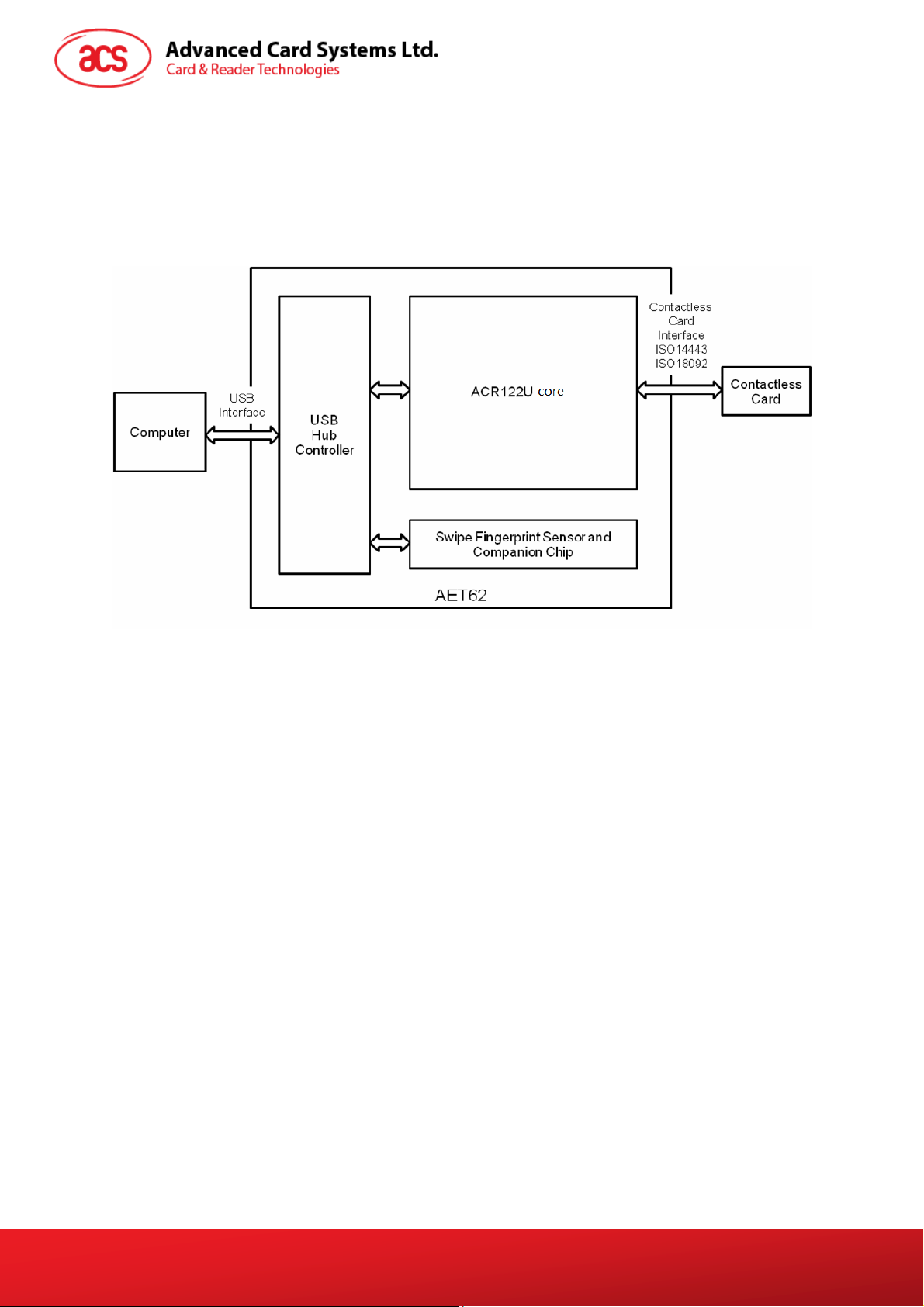
The AET62 is a composite device, consisting ACS’ ACR122U NFC Reader’s core and UPEK’s swipe
fingerprint sensor. The NFC contactless smart card reader and the fingerprint sensor can be used
independently, but combining the two technologies provide a higher level of security in applications.
The AET62’s system diagram is shown below:
Figure 1: AET62 System Block Diagram
The purpose of this document is to describe the architecture and interface of AET62’s contactless
smart card reader module, which is based on the ACR122U core. For information on the architecture
and programming interface of the fingerprint module, please refer to the AET62 Fingerprint Reader
Application Programming Interface document (API_AET62_v1.0).
AET62 Reference Manual
Document Title Here
Document Title Here
Version 1.00
Document Title Here
Page 5 of 35
info@acs.com.hk
www.acs.com.hk
Page 6
2.0. AET62 Contactless Smart Card Reader
The AET62 is a PC-linked contactless smart card reader/writer used for accessing ISO14443-4 Type
A and B, Mifare, ISO 18092 or NFC, and FeliCa tags. The AET62 Smart Card Reader is PCSCcompliant so it is compatible with existing PCSC applications. Furthermore, the standard Microsoft
CCID driver is used to simplify driver installation.
The AET62 serves as the mediating device between the personal computer and the contactless tag
via the USB interface. The reader carries out the command issued from the PC, whether the
command is used in order to communicate with a contactless tag or control the device peripherals (i.e.
bi-color LED).
The AET62 uses the PCSC APDUs for contactless tags following the PCSC Specification and makes
use of pseudo APDUs in sending commands for ISO 18092 tags and controlling the device
peripherals. This document will discuss how you can use the AET62 in your smart card system.
2.1. USB Interface
The AET62 is connected to a computer through USB as specified in the USB Specification 1.1. The
AET62 is working in Full speed mode, i.e. 12 Mbps.
Pin Signal Function
1 V
2 D3 D+
4 GND
BUS
+5V power supply for the reader (Max 200 mA, Normal 100 mA)
Differential signal transmits data between AET62 and PC.
Differential signal transmits data between AET62 and PC.
Reference voltage level for power supply
Table 1: USB Interface
AET62 Reference Manual
Document Title Here
Document Title Here
Version 1.00
Document Title Here
Page 6 of 35
info@acs.com.hk
www.acs.com.hk
Page 7
3.0. Implementation
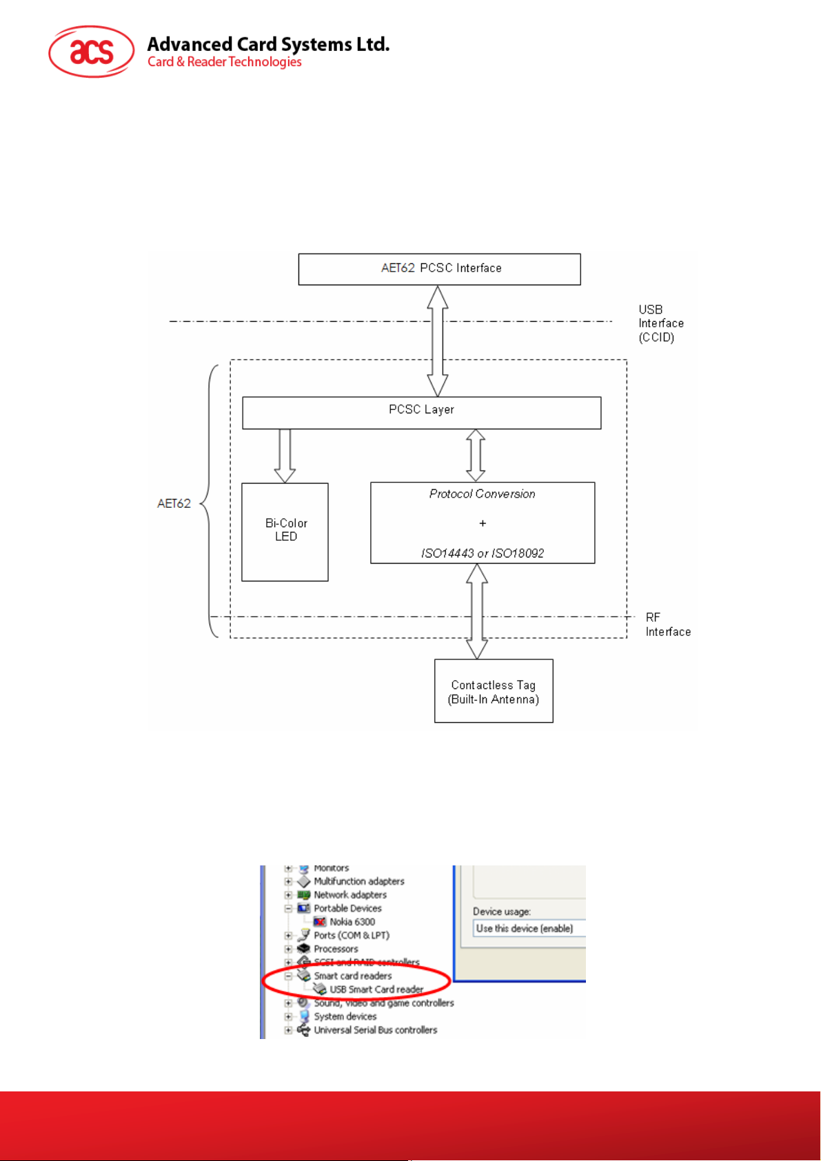
3.1. Communication Flow Chart of AET62
The Standard Microsoft CCID and PCSC drivers are used. Therefore, no ACS drivers are required
because the drivers are already built inside the windows operating system. You need to modify your
computer’s registry settings to be able to use the full capabilities of the AET62 NFC Reader. See
AET62 PCSC Escape
Command for more details.
3.2. Smart Card Reader Interface Overview
Just click the “Device Manager” to find out the “AET62 PICC Interface”. The standard Microsoft USB
CCID Driver is used.
AET62 Reference Manual
Document Title Here
Document Title Here
Version 1.00
Figure 2: Communication Flow Chart of AET62
Document Title Here
Page 7 of 35
info@acs.com.hk
www.acs.com.hk
Page 8
4.0. PICC Interface Description
4.1. ATR Generation
If the reader detects a PICC, an ATR will be sent to the PCSC driver to identify the PICC.
4.1.1. ATR format for ISO 14443 Part 3 PICCs
Byte
Value
(Hex)
Designation Description
0 3B Initial Header
1 8N T0 Higher nibble 8 means: no TA1, TB1, TC1
only TD1 is following.
Lower nibble N is the number of historical
bytes (HistByte 0 to HistByte N-1)
2 80 TD1 Higher nibble 8 means: no TA2, TB2, TC2
only TD2 is following.
Lower nibble 0 means T = 0
3 01 TD2 Higher nibble 0 means no TA3, TB3, TC3,
TD3 following.
Lower nibble 1 means T = 1
4
To
3+N
80 T1 Category indicator byte, 80 means A status
indicator may be present in an optional
COMPACT-TLV data object
4F Application identifier Presence Indicator
Tk
0C Length
RID Registered Application Provider Identifier
(RID) # A0 00 00 03 06
SS Byte for standard
C0 .. C1
Bytes for card name
00 00 00 00 RFU RFU # 00 00 00 00
4+N UU TCK Exclusive-oring of all the bytes T0 to Tk
Table 2: ATR format for ISO 14443 Part 3 PICCs
Example: ATR for MIfare 1K = {3B 8F 80 01 80 4F 0C A0 00 00 03 06 03 00 01 00 00 00 00 6A}
Initial
Header
3B 8F 80 01 80 4F 0C A0 00 00
ATR
T0 TD1 TD2 T1 Tk Length RID Standard Card
03 00 01 00 00 00
03 06
Where: Length (YY) = 0C
RID = A0 00 00 03 06 (PC/SC Workgroup)
Standard (SS) = 03 (ISO14443A, Part 3)
Card Name (C0 .. C1) = [00 01] (Mifare 1K)
Where, Card Name (C0 .. C1)
00 01: Mifare 1K
00 02: Mifare 4K
00 03: Mifare Ultralight
00 26: Mifare Mini
….
F0 04: Topaz and Jewel
F0 11: FeliCa 212K
F0 12: FeliCa 424K
…
FF [SAK]: Undefined
RFU TCK
Name
00
6A
AET62 Reference Manual
Document Title Here
Document Title Here
Version 1.00
Document Title Here
Page 8 of 35
info@acs.com.hk
www.acs.com.hk
Page 9
4.1.2. ATR format for ISO 14443 Part 4 PICCs
Byte Value
Designation Description
(Hex)
0 3B Initial Header
1 8N T0 Higher nibble 8 means: no TA1, TB1, TC1
only TD1 is following.
Lower nibble N is the number of historical
bytes (HistByte 0 to HistByte N-1)
2 80 TD1 Higher nibble 8 means: no TA2, TB2, TC2
only TD2 is following.
Lower nibble 0 means T = 0
3 01 TD2 Higher nibble 0 means no TA3, TB3, TC3,
TD3 following.
Lower nibble 1 means T = 1
to
3 + N
XX T1 4
XX
XX
XX
Tk
Historical Bytes:
ISO14443A:
The historical bytes from ATS response. Refer
to the ISO14443-4 specification.
ISO14443B:
The higher layer response from the ATTRIB
response (ATQB). Refer to the ISO14443-3
specification.
4+N UU TCK Exclusive-oring of all the bytes T0 to Tk
Table 3: ATR format for ISO 14443 Part 4 PICCs
We take for example, an ATR for DESFire which is:
DESFire (ATR) = 3B 86 80 01 06 75 77 81 02 80 00
ATR
Initial Header T0 TD1 TD2
3B 86 80 01 06 75 77 81 02 80 00
ATS
T1 Tk TCK
This ATR has 6 bytes of ATS which is: [06 75 77 81 02 80]
Note: Use the APDU “FF CA 01 00 00” to distinguish the ISO14443A-4 and ISO14443B-4
PICCs, and retrieve the full ATS if available. The ATS is returned for ISO14443A-3 or
ISO14443B-3/4 PICCs.
Another example would be the ATR for ST19XRC8E which is:
ST19XRC8E (ATR) = 3B 8C 80 01 50 12 23 45 56 12 53 54 4E 33 81 C3 55
ATR
Initial Header T0 TD1 TD2
3B 86 80 01 50 12 23 45 56 12 53 54 4E 33 81 C3 55
ATQB
T1 Tk TCK
Since this card follows ISO 14443 Type B, the response would be ATQB which is 50 12 23 45 56 12
53 54 4E 33 81 C3 is 12 bytes long with no CRC-B
Note: You can refer to the ISO7816, ISO14443 and PCSC standards for more details.
Page 9 of 35
AET62 Reference Manual
Document Title Here
Document Title Here
Version 1.00
Document Title Here
info@acs.com.hk
www.acs.com.hk
Page 10
5.0. PICC Commands for General Purposes
5.1. Get Data
The “Get Data command” will return the serial number or ATS of the “connected PICC”.
Command Class INS P1 P2 Le
Get Data FF CA
Table 4: Get UID APDU Format (5 Bytes)
Response Data Out
Result UID
(LSB)
Table 5: Get UID Response Format (UID + 2 Bytes) if P1 = 0x00
Response Data Out
Result ATS SW1 SW2
00
01
00
UID
(MSB)
(Full Length)
SW1 SW2
00
Table 6: Get ATS of a ISO 14443 A card (ATS + 2 Bytes) if P1 = 0x01
Results SW1 SW2 Meaning
Success 90 00
Error 63 00
Error 6A 81
Example:
1. To get the serial number of the “connected PICC”
UINT8 GET_UID[5]={0xFF, 0xCA, 0x00, 0x00, 0x04};
2. To get the ATS of the “connected ISO 14443 A PICC”
UINT8 GET_ATS[5]={0xFF, 0xCA, 0x01, 0x00, 0x04};
The operation is completed successfully.
The operation is failed.
Function not supported.
Table 7: Response Codes
AET62 Reference Manual
Document Title Here
Document Title Here
Version 1.00
Document Title Here
Page 10 of 35
info@acs.com.hk
www.acs.com.hk
Page 11
6.0. PICC Commands (T=CL Emulation) for Mifare Classic
Memory Cards
6.1. Load Authentication Keys
The “Load Authentication Keys command” will load the authentication keys into the reader. The
authentication keys are used to authenticate the particular sector of the Mifare 1K/4K Memory Card.
Two kinds of authentication key locations are provided, volatile and non-volatile key locations
respectively.
Command Class INS P1 P2 Lc Data In
Load
Authentication
Keys
Table 8: Load Authentication Keys APDU Format (11 Bytes)
Key Structure (1 Byte):
0x00 = Key is loaded into the reader volatile memory.
Other = Reserved.
Key Number (1 Byte):
0x00 ~ 0x01 = Key Location. The keys will disappear once the reader is disconnected from the
PC.
Key (6 Bytes):
The key value loaded into the reader. E.g. {FF FF FF FF FF FF}
Table 9: Load Authentication Keys Response Format (2 Bytes)
Results SW1 SW2 Meaning
Success 90 00
Error 63 00
Table 10: Load Authentication Keys Response Codes
Example:
Load a key {FF FF FF FF FF FF} into the key location 0x00.
APDU = {FF 82 00 00 06 FF FF FF FF FF FF}
FF 82
Response Data Out
Result SW1 SW2
The operation is completed successfully.
The operation is failed.
Key
Structure
Key
Number
06
Key
(6
bytes)
AET62 Reference Manual
Document Title Here
Document Title Here
Version 1.00
Document Title Here
Page 11 of 35
info@acs.com.hk
www.acs.com.hk
Page 12

6.2. Authentication
The “Authentication command” uses the keys stored in the reader to execute authentication with the
Mifare 1K/4K card (PICC). Two types of authentication keys are used: TYPE_A and TYPE_B.
Command Class INS P1 P2 P3 Data In
Authentication FF 88 00 Block Number
Table 11: Load Authentication Keys APDU Format (6 Bytes) [Obsolete]
Command Class INS P1 P2 Lc Data In
Authentication FF 86 00 00 05 Authenticate Data Bytes
Table 12: Load Authentication Keys APDU Format (10 Bytes)
Byte1 Byte 2 Byte 3 Byte 4 Byte 5
Version
0x01
0x00
Block
Number
Key Type Key Number
Table 13: Authenticate Data Bytes (5 Byte)
Key
Type
Key Number
Block Number: 1 Byte. This is the memory block to be authenticated.
Key Type: 1 Byte
0x60 = Key is used as a TYPE A key for authentication.
0x61 = Key is used as a TYPE B key for authentication.
Key Number: 1 Byte
0x00 ~ 0x1F = Key Location.
Note: For Mifare 1K Card, there are 16 sectors and each sector consists of 4 consecutive
blocks. E.g. Sector 0x00 consists of Blocks {0x00, 0x01, 0x02 and 0x03}; Sector 0x01 consists
of Blocks {0x04, 0x05, 0x06 and 0x07}; the last sector 0x0F consists of Blocks {0x3C, 0x3D,
0x3E and 0x3F}.
Once the authentication is executed successfully, there is no need to execute the authentication again
provided that the blocks to be accessed are belonging to the same sector. Please refer to the Mifare
1K/4K specification for more details.
Response Data Out
Result SW1 SW2
Table 14: Load Authentication Keys Response Format (2 Bytes)
Results SW1 SW2 Meaning
Success 90 00
Error 63 00
Table 15: Load Authentication Keys Response Codes
The operation is completed successfully.
The operation is failed.
AET62 Reference Manual
Document Title Here
Document Title Here
Version 1.00
Document Title Here
Page 12 of 35
info@acs.com.hk
www.acs.com.hk
Page 13

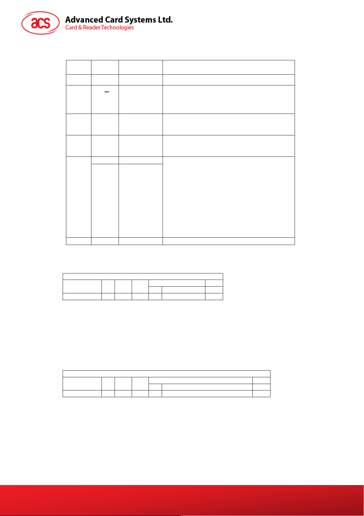
Mifare 1K Memory Map.
Sectors
(Total 16 sectors. Each sector
consists of 4 consecutive blocks)
Sector 0 0x00 ~ 0x02 0x03
Sector 1 0x04 ~ 0x06 0x07
..
..
Sector 14 0x38 ~ 0x0A 0x3B
Sector 15 0x3C ~ 0x3E 0x3F
Mifare 4K Memory Map.
Sectors
(Total 32 sectors. Each sector
consists of 4 consecutive blocks)
Sector 0 0x00 ~ 0x02 0x03
Sector 1 0x04 ~ 0x06 0x07
..
..
Sector 30 0x78 ~ 0x7A 0x7B
Sector 31 0x7C ~ 0x7E 0x7F
Sectors
(Total 8 sectors. Each sector
consists of 16 consecutive
blocks)
Sector 32 0x80 ~ 0x8E 0x8F
Sector 33 0x90 ~ 0x9E 0x9F
..
..
Sector 38 0xE0 ~ 0xEE 0xEF
Sector 39 0xF0 ~ 0xFE 0xFF
Data Blocks
(3 blocks, 16 bytes per
block)
Data Blocks
(3 blocks, 16 bytes per
block)
Data Blocks
(15 blocks, 16 bytes per
block)
Trailer Block
(1 block, 16 bytes)
1K
Bytes
Trailer Block
(1 block, 16 bytes)
2K
Bytes
Trailer Block
(1 block, 16 bytes)
2K
Bytes
Mifare Ultralight Memory Map.
AET62 Reference Manual
Document Title Here
Document Title Here
Version 1.00
Byte Number
Serial Number SN0 SN1 SN2 BCC0 0
Serial Number SN3 SN4 SN5 SN6 1
Internal / Lock BCC1 Internal Lock0 Lock1 2
OTP OPT0 OPT1 OTP2 OTP3 3
Data read/write Data0 Data1 Data2 Data3 4
Data read/write Data4 Data5 Data6 Data7 5
Data read/write Data8 Data9 Data10 Data11 6
Data read/write Data12 Data13 Data14 Data15 7
Data read/write Data16 Data17 Data18 Data19 8
Data read/write Data20 Data21 Data22 Data23 9
Data read/write Data24 Data25 Data26 Data27 10
Data read/write Data28 Data29 Data30 Data31 11
Data read/write Data32 Data33 Data34 Data35 12
Data read/write Data36 Data37 Data38 Data39 13
Data read/write Data40 Data41 Data42 Data43 14
Data read/write Data44 Data45 Data46 Data47 15
0 1 2 3 Page
Document Title Here
512 bits
Or
64 Bytes
Page 13 of 35
info@acs.com.hk
www.acs.com.hk
Page 14

Example:
1. To authenticate the Block 0x04 with a {TYPE A, key number 0x00}. For PC/SC V2.01,
Obsolete.
APDU = {FF 88 00 04 60 00};
2. To authenticate the Block 0x04 with a {TYPE A, key number 0x00}. For PC/SC V2.07
alaAPDU = {FF 86 00 00 05 01 00 04 60 00}
Note: Mifare Ultralight does not need to execute any authentication. The memory is free to access.
AET62 Reference Manual
Document Title Here
Document Title Here
Version 1.00
Document Title Here
Page 14 of 35
info@acs.com.hk
www.acs.com.hk
Page 15

6.3. Read Binary Blocks
The “Read Binary Blocks command” is used for retrieving “data blocks” from the PICC. The data
block/trailer block must be authenticated first.
Command
Read Binary Blocks FF B0 00 Block Number Number of Bytes to
where:
Block Number (1 Byte): The block to be accessed
Number of Bytes to Read (1 Byte): Maximum 16 bytes
Response
Result
Table 17: Read Binary Block Response Format (N + 2 Bytes)
Results SW1 SW2 Meaning
Success 90 00
Error 63 00
Example:
1. Read 16 bytes from the binary block 0x04 (Mifare 1K or 4K)
APDU = {FF B0 00 04 10}
2. Read 4 bytes from the binary Page 0x04 (Mifare Ultralight)
APDU = {FF B0 00 04 04}
3. Read 16 bytes starting from the binary Page 0x04 (Mifare Ultralight) (Pages 4, 5, 6 and 7 will
be read)
APDU = {FF B0 00 04 10}
Class INS P1 P2 Le
Table 16: Read Binary APDU Format (5 Bytes)
Data Out
0 <= N <= 16
The operation completed successfully.
The operation failed.
Table 18: Read Binary Block Response Codes
SW1 SW2
Read
AET62 Reference Manual
Document Title Here
Document Title Here
Version 1.00
Document Title Here
Page 15 of 35
info@acs.com.hk
www.acs.com.hk
Page 16

6.4. Update Binary Blocks
The “Update Binary Blocks command” is used for writing “data blocks” into the PICC. The data
block/trailer block must be authenticated.
Command
Update
Binary
Blocks
where:
Block Number (1 Byte):The starting block to be updated.
Number of Bytes to Update (1 Byte):
16 bytes for Mifare 1K/4K
4 bytes for Mifare Ultralight.
Block Data (4 or 16 Bytes):
The data to be written into the binary block/blocks.
Results SW1 SW2 Meaning
Success 90 00
Error
Example:
1. Update the binary block 0x04 of Mifare 1K/4K with Data {00 01 .. 0F}
APDU = {FF D6 00 04 10 00 01 02 03 04 05 06 07 08 09 0A 0B 0C 0D 0E
2. Update the binary block 0x04 of Mifare Ultralight with Data {00 01 02 03}
APDU = {FF D6 00 04 04 00 01 02 03}
Class INS P1 P2 Lc Data In
FF D6 00 Block
Number
Table 19: Update Binary APDU Format (4 or 16 + 5 Bytes)
The operation completed
successfully.
Table 20: Update Binary Block Response Codes (2 Bytes)
63 00
0F}
The operation failed.
Number
of
Bytes
to
Update
16 Bytes for
Mifare 1K/4K
Block Data
4 Bytes for
Mifare
Ultralight
or
6.5. Value Block Related Commands
The data block can be used as value block for implementing value-based applications.
6.5.1. Value Block Operation
The “Value Block Operation command” is used for manipulating value-based transactions. E.g.
Increment a value of the value block etc.
Block Number (1 Byte): The value block to be manipulated.
VB_OP (1 Byte):
AET62 Reference Manual
Document Title Here
Document Title Here
Version 1.00
Command
Value
Block
Operation
Class INS P1 P2 Lc Data In
FF D7 00 Block
Number
Table 21: Value Block Operation APDU Format (10 Bytes)
Document Title Here
05 VB_OP VB_Value
(4 Bytes)
{MSB .. LSB}
Page 16 of 35
info@acs.com.hk
www.acs.com.hk
Page 17

0x00 = Store the VB_Value into the block. The block will then be converted to a value
block.
0x01 = Increment the value of the value block by the VB_Value. This command is
only valid for value block.
0x02 = Decrement the value of the value block by the VB_Value. This command is
only valid for value block.
VB_Value (4 Bytes): The value used for value manipulation. The value is a signed long
integer (4 bytes).
Example 1: Decimal –4 = {0xFF, 0xFF, 0xFF, 0xFC}
VB_Value
MSB
LSB
FF FF FF FC
Example 2: Decimal 1 = {0x00, 0x00, 0x00, 0x01}
VB_Value
MSB LSB
00 00 00 01
Response Data Out
Result SW1 SW2
Table 22: Value Block Operation Response Format (2 Bytes)
Results SW1 SW2 Meaning
Success 90 00
Error 63 00
The operation completed successfully.
The operation failed.
Table 23: Value Block Operation Response Codes
6.5.2. Read Value Block
The “Read Value Block command” is used for retrieving the value from the value block. This
command is only valid for value block.
Command Class INS P1 P2 Le
Read Value Block FF B1 00 Block Number 04
Table 24: Read Value Block APDU Format (5 Bytes)
Block Number (1 Byte): The value block to be accessed.
Response Data Out
Result
Table 25: Read Value Block Response Format (4 + 2 Bytes)
Value (4 Bytes): The value returned from the card. The value is a signed long integer (4
bytes).
Example 1: Decimal –4 = {0xFF, 0xFF, 0xFF, 0xFC}
Value
MSB LSB
FF FF FF FC
Example 2: Decimal 1 = {0x00, 0x00, 0x00, 0x01}
Value
MSB LSB
00 00 00 01
Value
{MSB ..
LSB}
SW1 SW2
AET62 Reference Manual
Document Title Here
Document Title Here
Version 1.00
Document Title Here
Page 17 of 35
info@acs.com.hk
www.acs.com.hk
Page 18

Results SW1 SW2 Meaning
Success 90 00
Error 63 00
The operation is completed successfully.
The operation is failed.
Table 26: Read Value Block Response Codes
6.5.3. Restore Value Block
The “Restore Value Block command” is used to copy a value from a value block to another value
block.
Command Class INS P1 P2 Lc Data In
Value Block
Operation
Source Block Number (1 Byte): The value of the source value block will be copied to the
Target Block Number (1 Byte): The value block to be restored. The source and target value
Table 28: Restore Value Block Response Format (2 Bytes)
FF D7 00 Source
Block
Number
02 03 Target
Block
Number
Table 27: Restore Value Block APDU Format (7 Bytes)
target value block.
blocks must be in the same sector.
Response Data Out
Result SW1 SW2
Results SW1 SW2 Meaning
Success 90 00
Error 63 00
The operation is completed successfully.
The operation is failed.
Table 29: Restore Value Block Response Codes
Example:
1. Store a value “1” into block 0x05
APDU = {FF D7 00 05 05 00 00 00 00 01}
Answer: 90 00
2. Read the value block 0x05
APDU = {FF B1 00 05 00}
Answer: 00 00 00 01 90 00 [9000]
3. Copy the value from value block 0x05 to value block 0x06
APDU = {FF D7 00 05 02 03 06}
Answer: 90 00 [9000]
4. Increment the value block 0x05 by “5”
APDU = {FF D7 00 05 05 01 00 00 00 05}
Answer: 90 00 [9000]
AET62 Reference Manual
Document Title Here
Document Title Here
Version 1.00
Document Title Here
Page 18 of 35
info@acs.com.hk
www.acs.com.hk
Page 19

7.0. Pseudo-APDUs
Pseudo-APDUs are used for the following:
Exchanging Data with Non-PCSC Compliant Tags.
Retrieving and setting the reader parameters.
The Pseudo-APDUs can be sent through the “AET62 PICC Interface” if the tag is already
connected.
Or the Pseudo-APDUs can be sent by using “Escape Command ” if the tag is not presented
yet.
7.1. Direct Transmit
This is the Payload to be sent to the tag or reader.
Command Class INS P1 P2 Lc Data In
Direct
Transmit
Table 30: Direct Transmit Command Format (Length of the Payload + 5 Bytes)
Lc: Number of Bytes to Send (1 Byte)
Maximum 255 bytes
Data In: Response
0xFF 0x00 0x00 0x00
Response Data Out
Direct Transmit Response Data
Table 31: Direct Transmit Response Format
Number
of Bytes
to send
Payload
7.2. Bi-Color LED Control
This APDU is used to control the states of the Bi-Color LED.
Command Class INS P1 P2 Lc
Bi-Color
LED
Control
P2: LED State Control
CMD Item Description
Bit 0 Final Red LED State 1 = On; 0 = Off
Bit 1 Final Green LED State 1 = On; 0 = Off
Bit 2 Red LED State Mask
Bit 3 Green LED State Mask
Bit 4 Initial Red LED Blinking State 1 = On; 0 = Off
Bit 5 Initial Green LED Blinking State 1 = On; 0 = Off
Bit 6 Red LED Blinking Mask
Bit 7 Green LED Blinking Mask
0xFF 0x00 0x40 LED
State
Control
Table 32: Bi-Color LED Control Command Format (9 Bytes)
Table 33: Bi-Color LED Control Format (1 Byte)
Data In
(4 Bytes)
0x04 Blinking
Duration
Control
1 = Update the State
0 = No change
1 = Update the State
0 = No change
1 = Blink
0 = Not Blink
1 = Blink
0 = Not Blink
AET62 Reference Manual
Document Title Here
Document Title Here
Version 1.00
Document Title Here
Page 19 of 35
info@acs.com.hk
www.acs.com.hk
Page 20

Data In: Blinking Duration Control
Byte 0 Byte 1 Byte 2 Byte 3
T1 Duration
Initial Blinking State
(Unit = 100ms)
Table 34: Bi-Color LED Blinking Duration Control Format (4 Bytes)
Data Out: SW1 SW2. Status Code returned by the reader.
Results SW1 SW2 Meaning
Success 90
Error
Status Item Description
Bit 0 Current Red LED 1 = On; 0 = Off
Bit 1 Current Green LED 1 = On; 0 = Off
Bits 2 – 7 Re served
63 00
T2 Duration
Toggle Blinking State
(Unit = 100ms)
Current LED
State
Table 35: Status Code
Table 36: Current LED State (1 Byte)
Number of
repetition
The operation is completed successfully.
The operation is failed.
0x00
Note:
The LED State operation will be performed after the LED Blinking operation is completed.
The LED will not be changed if the corresponding LED Mask is not enabled.
The LED will not be blinking if the corresponding LED Blinking Mask is not enabled. Also, the
number of repetition must be greater than zero.
T1 and T2 duration parameters are used for controlling the duty cycle of LED blinking. For
example, if T1=1 and T2=1, the duty cycle = 50%. #Duty Cycle = T1 / (T1 + T2).
7.3. Get the Firmware Version of the reader
This is used to retrieve the firmware version of the reader.
Command Class INS P1 P2 Le
Get
Response
Response Data Out
Result Firmware Version
E.g. Response = 41 45 54 36 32 30 33 30 30 (Hex) = AET620300 (ASCII)
0xFF 0x00 0x48 0x00 0x00
Table 37: Command Format (5 Bytes)
Table 38: Response Format (10 bytes)
7.4. Get the PICC Operating Parameter
This is used to retrieve the PICC Operating Parameter of the reader.
AET62 Reference Manual
Document Title Here
Document Title Here
Version 1.00
Command
Get
Response
Class INS P1 P2 Le
0xFF 0x00 0x50 0x00 0x00
Table 39: Command Format (5 Bytes)
Document Title Here
Page 20 of 35
info@acs.com.hk
www.acs.com.hk
Page 21

Response Data Out
Result PICC Operating Parameter
Table 40: Response Format (1 byte)
7.5. Set the PICC Operating Parameter
This is used to set the PICC Operating Parameter of the reader.
Command Class INS P1 P2 Le
Get
Response
Response Data Out
Bit Parameter Description Option
7 Auto PICC Polling To enable the PICC Polling
6 Auto ATS Generation
5 Polling Interval
4 FeliCa 424K
3 FeliCa 212K
2 Topaz
1 ISO14443 Type B
ISO14443 Type A
#To detect the Mifare
0
Tags, the Auto ATS
Generation must be
disabled first.
0xFF 0x00 0x51
Table 41: Command Format (5 Bytes)
Result PICC Operating Parameter
Table 42: Response Format (1 byte)
To issue ATS Request whenever an
ISO14443-4 Type A tag is activated
To set the time interval between
successive PICC Polling.
The Tag Types to be detected
during PICC Polling.
Table 43: PICC Operating Parameter. Default Value = FF
New PICC
Operating
Parameter
0x00
1 = Enable
0 = Disable
1 = Enable
0 = Disable
1 = 250 ms
0 = 500 ms
1 = Detect
0 = Skip
1 = Detect
0 = Skip
1 = Detect
0 = Skip
1 = Detect
0 = Skip
1 = Detect
0 = Skip
AET62 Reference Manual
Document Title Here
Document Title Here
Version 1.00
Document Title Here
Page 21 of 35
info@acs.com.hk
www.acs.com.hk
Page 22

8.0. Basic Program Flow for Contactless Applications
Step 0. Start the application. The reader will do the PICC Polling and scan for tags continuously.
Once the tag is found and detected, the corresponding ATR will be sent to the PC. You must
make sure that the PCSC Escape Command has been set. See AET62 PCSC Esc
Command for more details.
Step 1. The first thing i
Step 2. Access the PICC by sending APDU commands.
:
:
Step N. Disconnect the “AET62 PICC Interface”. Shut down the application.
NOTE:
1. The antenna can be switched off in order to save the power.
Turn off the antenna power: FF 00 00 00 04 D4 32 01 00
Turn on the antenna power: FF 00 00 00 04 D4 32 01 01
2. Standard and Non-Standard APDUs Handling.
PICCs that use Standard APDUs: ISO14443-4 Type A and B, Mifare .. etc
PICCs that use Non-Standard APDUs: FeliCa, Topaz .. etc.
s to connect the “AET62 PICC Interface”.
ape
1) For the AET62 PICC Interface, ISO7816 T=1 protocol is used.
o PC Reader: Issue an APDU to the reader.
o Reader PC: The response data is returned.
AET62 Reference Manual
Document Title Here
Document Title Here
Version 1.00
Figure 3: Basic Program Flow for Contactless Applications
Document Title Here
Page 22 of 35
info@acs.com.hk
www.acs.com.hk
Page 23

8.1. How to Access PCSC-Compliant Tags (ISO 14443-4)?
Basically, all ISO 14443-4 compliant cards (PICCs) would understand the ISO 7816-4 APDUs. The
AET62 Reader just has to communicate with the ISO 14443-4 compliant cards through exchanging
ISO 7816-4 APDUs and Responses. AET62 will handle the ISO 14443 Parts 1-4 Protocols internally.
Mifare 1K, 4K, MINI and Ultralight tags are supported through the T=CL emulation. Just simply treat
the Mifare tags as standard ISO 14443-4 tags. For more information, please refer to topic “PICC
Commands for Mifare Classic Memory Tags”.
Command Class INS P1 P2 Lc
ISO 7816
Part 4
Command
Response Data Out
Result Response Data SW1 SW2
Results SW1 SW2 Meaning
Success 90 00
Error
Typical sequence may be:
- Present the Tag and Connect the PICC Interface
- Read / Update the memory of the tag
Step 1) Connect the Tag
Step 2) Send an APDU, Get Challenge.
<< 00 84 00 00 08
>> 1A F7 F3 1B CD 2B A9 58 [90 00]
Hint:
For ISO14443-4 Type A tags, the ATS can be obtained by using the APDU “FF CA 00 00 01”
Table 44: ISO 7816-4 APDU Format
Table 45: ISO 7816-4 Response Format (Data + 2 Bytes)
The operation is completed successfully.
63 00
Table 46: Common ISO 7816-4 Response Codes
The operation is failed.
Length
of the
Data
In
Data
In
Le
Expected
length
of the
Response
Data
AET62 Reference Manual
Document Title Here
Document Title Here
Version 1.00
Document Title Here
Page 23 of 35
info@acs.com.hk
www.acs.com.hk
Page 24

8.2. How to Access DESFire Tags (ISO 14443-4)?
DESFire supports ISO 7816-4 APDU Wrapping and Native modes. Once the DESFire Tag is
activated, the first APDU sent to the DESFire Tag will determine the “Command Mode”. If the first
APDU is in “Native Mode”, the rest of the APDUs must be in “Native Mode” format. Similarly, if the first
APDU is in “ISO 7816-4 APDU Wrapping Mode”, the rest of the APDUs must be in “ISO 7816-4
APDU Wrapping Mode” format.
Example 1: DESFire ISO 7816-4 APDU Wrapping
To read 8 bytes random number from an ISO 14443-4 Type A PICC (DESFire)
APDU = {90 0A 00 00 01 00 00}
Class = 0x90; INS = 0x0A (DESFire Instruction); P1 = 0x00; P2 = 0x00
Lc = 0x01; Data In = 0x00; Le = 0x00 (Le = 0x00 for maximum length)
Answer: 7B 18 92 9D 9A 25 05 21 [$91AF]
The Status Code [91 AF] is defined in DESFire specification. Please refer to the DESFire
specification for more details.
Example 2: DESFire Frame Level Chaining (ISO 7816 wrapping mode)
In this example, the application has to do the “Frame Level Chaining”. To get the version of
the DESFire card.
Step 1: Send an APDU {90 60 00 00 00} to get the first frame. INS=0x60
Answer: 04 01 01 00 02 18 05 91 AF [$91AF]
Step 2: Send an APDU {90 AF 00 00 00} to get the second frame. INS=0xAF
Answer: 04 01 01 00 06 18 05 91 AF [$91AF]
Step 3: Send an APDU {90 AF 00 00 00} to get the last frame. INS=0xAF
Answer: 04 52 5A 19 B2 1B 80 8E 36 54 4D 40 26 04 91 00 [$9100]
Example 3: DESFire Native Command
We can send Native DESFire Commands to the reader without ISO 7816 wrapping if we find
that the Native DESFire Commands are easier to handle.
To read 8 bytes random number from an ISO 14443-4 Type A PICC (DESFire)
APDU = {0A 00}
Answer: AF 25 9C 65 0C 87 65 1D D7[$1DD7]
In which, the first byte “AF” is the status code returned by the DESFire Card.
The Data inside the blanket [$1DD7] can simply be ignored by the application.
Example 4: DESFire Frame Level Chaining (Native Mode)
In this example, the application has to do the “Frame Level Chaining”.
To get the version of the DESFire card.
Step 1: Send an APDU {60} to get the first frame. INS=
wer: AF 04 01 01 00 02 18 05[$1805]
Ans
Step 2: Send an APDU {AF} to get the second frame. INS=0xAF
Answer: AF 04 01 01 00 06 18 05[$1805]
Step 3: Send an APDU {AF} to get the last frame. INS=0xAF
Answer: 00 04 52 5A 19 B2 1B 80 8E 36 54 4D 40 26 04[$2604]
0x60
Note: In DESFire Native Mode, the status code [90 00] will not be added to the response if
the response length is greater than 1. If the response length is less than 2, the status code
[90 00] will be added in order to meet the requirement of PCSC. The minimum response
length is 2.
AET62 Reference Manual
Document Title Here
Document Title Here
Version 1.00
Document Title Here
Page 24 of 35
info@acs.com.hk
www.acs.com.hk
Page 25

8.3. How to Access FeliCa Tags (ISO 18092)?
Typical sequence may be:
- Present the FeliCa Tag and Connect the PICC Interface
- Read / Update the memory of the tag
Step 1) Connect the Tag
The ATR = 3B 8F 80 01 80 4F 0C A0 00 00 03 06 03 F0 11 00 00 00 00 8A
In which,
F0 11 = FeliCa 212K
Step 2) Read the memory block without using Pseudo APDU.
<< 10 06 [8-byte NFC ID] 01 09 01 01 80 00
>> 1D 07 [8-byte NFC ID] 00 00 01 00 AA 55 AA 55 AA 55 AA 55 AA 55 AA 55
AA 55 AA [90 00]
Or
Step 2) Read the memory block using Pseudo APDU.
<< FF 00 00 00 [13] D4 40 01 10 06 [8-byte NFC ID] 01 09 01 01 80 00
In which,
[13] is the length of the Pseudo Data “D4 40 01.. 80 00”
D4 40 01 is the Data Exchange Command
>> D5 41 00 1D 07 [8-byte NFC ID] 00 00 01 00 AA 55 AA 55 AA 55 AA 55 AA
55 AA 55 AA 55 AA [90 00]
In which, D5 41 00 is the Data Exchange Response
Note: The NFC ID can be obtained by using the APDU “FF CA 00 00 00”
Please refer to the FeliCa specification for more detailed information.
8.4. How to Access NFC Forum Type 1 Tags (ISO 18092), e.g. Jewel and Topaz Tags?
Typical sequence may be:
- Present the Topaz Tag and Connect the PICC Interface
- Read / Update the memory of the tag
Step 1) Connect the Tag
The ATR = 3B 8F 80 01 80 4F 0C A0 00 00 03 06 03 F0 04 00 00 00 00 9F
In which, F0 04 = Topaz
Step 2) Read the memory address 08 (Block 1: Byte-0) without using Pseudo APDU
<< 01 08
>> 18 [90 00]
In which, Response Data = 18
Or
Step 2) Read the memory address 08 (Block 1: Byte-0) using Pseudo APDU
<< FF 00 00 00 [05] D4 40 01 01 08
In which,
[05] is the length of the Pseudo APDU Data “D4 40 01 01 08”
D4 40 01 is the Data Exchange Command.
01 08 is the data to be sent to the tag.
>> D5 41 00 18 [90 00]
In which, Response Data = 18
AET62 Reference Manual
Document Title Here
Document Title Here
Version 1.00
Document Title Here
Page 25 of 35
info@acs.com.hk
www.acs.com.hk
Page 26

Tip: To read all the memory content of the tag
<< 00
>> 11 48 18 26 .. 00 [90 00]
Step 3) Update the memory address 08(Block 1: Byte-0)with the data FF
<< 53 08 FF
>> FF [90 00]
In which, Response Data = FF
Topaz Memory Map.
Memory Address = Block No * 8 + Byte No
e.g. Memory Address 08 (hex) = 1 x 8 + 0 = Block 1: Byte-0 = Data0
e.g. Memory Address 10 (hex) = 2 x 8 + 0 = Block 2: Byte-0 = Data8
Please refer to the Jewel and Topaz specifications documents for more detailed information.
AET62 Reference Manual
Document Title Here
Document Title Here
Version 1.00
Document Title Here
Page 26 of 35
info@acs.com.hk
www.acs.com.hk
Page 27

8.5. Get the Current Setting of the Contactless Interface
Step 1) Get Status Command
<< FF 00 00 00 02 D4 04
>> D5 05 [Err] [Field] [NbTg] [Tg] [BrRx] [BrTx] [Type] 80 90 00
Or if no tag is in the field
>> D5 05 00 00 00 80 90 00
[Err] is an error code corresponding to the latest error detected.
Field indicates if an external RF field is present and detected (Field = 0x01) or not (Field = 0x00).
[NbTg] is the number of targets. The default value is 1.
[Tg]: logical number
[BrRx] : bit rate in reception
0x00 : 106 kbps
0x01 : 212 kbps
0x02 : 424 kbps
[BrTx] : bit rate in transmission
0x00 : 106 kbps
0x01 : 212 kbps
0x02 : 424 kbps
[Type ]: modulation type
0x00 : ISO14443 or Mifare®
0x10 : FeliCa™
0x01 : Active mode
0x02 : Innovision Jewel® tag
AET62 Reference Manual
Document Title Here
Document Title Here
Version 1.00
Document Title Here
Page 27 of 35
info@acs.com.hk
www.acs.com.hk
Page 28

Appendix A. AET62 PCSC Escape Command
1. Select the “ACS AET62 PICC Interface 0”
2. Select the “Shared Mode” if the “AET62 PICC Interface” is already connected or “Direct Mode if
the “AET62 PICC Interface” is not connected.
3. Press the “Connect” button to establish a connection between the PC and the AET62 reader.
4. Enter “3500” in the Command text box
5. Enter the PCSC Escape Command, e.g. “FF 00 48 00 00” and press the “Send” button to send
the command to the reader. #Get the firmware version
6. Press the “Disconnect” button to break the connection.
7. In order to send or receive Escape commands to a reader, follow the instructions below
8. The vendor IOCTL for the Escape command is defined as follows:
#define IOCTL_CCID_ESCAPE SCARD_CTL_CODE(3500)
The following instructions enumerate the steps to enable the PCSC Escape command:
Execute the “RegEdit” in the “Run Command
Menu” of Windows
AET62 Reference Manual
Document Title Here
Document Title Here
Version 1.00
Document Title Here
Page 28 of 35
info@acs.com.hk
www.acs.com.hk
Page 29

Add a DWORD “EscapeCommandEnable” under
HKLM\SYSTEM\CCS\Enum\USB\Vid_072F&Pid_0
102\Device Parameters
For Vista, the path is:
Computer\HKEY_LOCAL_MACHINE\SYSTEMS\C
urrentControlSet\Enum\USB
Look for: VID_072F&PID_0102
Then expand the node. Look under Device
parameters
Create a DWORD entry (32-bit) with the name:
EscapeCommandEnable
AET62 Reference Manual
Document Title Here
Document Title Here
Version 1.00
Document Title Here
Page 29 of 35
info@acs.com.hk
www.acs.com.hk
Page 30

To Modify the value of the EscapeCommandEnable
double click on the entry and input 1 in the Value
data with the base set in Hexadecimal.
AET62 Reference Manual
Document Title Here
Document Title Here
Version 1.00
Document Title Here
Page 30 of 35
info@acs.com.hk
www.acs.com.hk
Page 31

Appendix B. APDU Command and Response Flow
for ISO 14443-Compliant Tags
Assume an ISO14443-4 Type B tag is used.
<< Typical APDU Command and Response Flow >>
PC
Reader
Tag
Sequences
1. The
command is
sent
USB Interface
(12Mbps)
Contactless
Related
Command
[APDU
Command]
e.g. [00 84
00 00 08]
(Get
Challenge)
RF Interface
(13.56MHz)
Tag-specific
Command
Frame
[APDU
Command]
embedded in
ISO14443
Frame
2. The
response is
received
Contactless
Related
Response
[APDU
Response]
e.g. [11 22
33 44 55 66
77 88] (90
00)
Tag-specific
Response
Frame
[APDU
Response]
embedded in
ISO14443
Frame
Page 31 of 35
AET62 Reference Manual
Document Title Here
Document Title Here
Version 1.00
Document Title Here
info@acs.com.hk
www.acs.com.hk
Page 32

Appendix C. APDU Command and Response Flow
for ISO 18092-Compliant Tags
Assume a TOPAZ tag is used.
<< Typical APDU Command and Response Flow >>
PC
Sequences
1. The command
is sent
Contactless Related
e.g. FF 00 00 00 05
D4 40 01 [01 08]
Reader
USB Interface
(12Mbps)
Command
[Native Command]
e.g. [01 08] (read
memory address 08)
or
Pseudo APDU
Command
+ [Native Command]
Tag-specific Command Frame
[Native Command] embedded in
Tag
RF Interface
(13.56MHz)
ISO18092 Frame
2. The response
is received
Contactless Related
Response
[Native Response]
e.g. 00 (90 00)
or
Pseudo APDU
Response
+ [Native Response]
e.g. D5 41 00 [00]
(90 00)
Tag-specific Response Frame
e.g. [Native Response]
embedded in
ISO18092 Frame
AET62 Reference Manual
Document Title Here
Document Title Here
Version 1.00
Document Title Here
Page 32 of 35
info@acs.com.hk
www.acs.com.hk
Page 33

Appendix D. Error Codes
Error Error Code
No Error 0x00
Time Out, the target has not answered
A CRC error has been detected by the contactless UART
A Parity error has been detected by the contactless UART
During a Mifare anti-collision/select operation, an erroneous Bit Count has been
detected
Framing error during Mifare operation
An abnormal bit-collision has been detected during bit wise anti-collision at 106
kbps
Communication buffer size insufficient
RF Buffer overflow has been detected by the contactless UART (bit BufferOvfl of
the register CL_ERROR)
In active communication mode, the RF field has not been switched on in time by the
counterpart (as defined in NFCIP-1 standard)
RF Protocol error (cf. reference [4], description of the CL_ERROR register)
Temperature error: the internal temperature sensor has detected overheating, and
therefore has automatically switched off the antenna drivers
Internal buffer overflow
Invalid parameter (range, format, …)
DEP Protocol: The chip configured in target mode does not support the command
received from the initiator (the command received is not one of the following:
ATR_REQ, WUP_REQ, PSL_REQ, DEP_REQ, DSL_REQ, RLS_REQ, ref. [1]).
DEP Protocol / Mifare / ISO/IEC 14443-4: The data format does not match to the
specification. Depending on the RF protocol used, it can be:
• Bad length of RF received frame,
• Incorrect value of PCB or PFB,
• Invalid or unexpected RF received frame,
• NAD or DID incoherence.
Mifare: Authentication error
ISO/IEC 14443-3: UID Check byte is wrong
DEP Protocol: Invalid device state, the system is in a state which does not allow the
operation
Operation not allowed in this configuration (host controller interface)
This command is not acceptable due to the current context of the chip (Initiator vs.
Target, unknown target number, Target not in the good state, …)
The chip configured as target has been released by its initiator
ISO/IEC 14443-3B only: the ID of the card does not match, meaning that the
expected card has been exchanged with another one.
ISO/IEC 14443-3B only: the card previously activated has disappeared.
Mismatch between the NFCID3 initiator and the NFCID3 target in DEP 212/424
kbps passive.
An over-current event has been detected
NAD missing in DEP frame
0x01
0x02
0x03
0x04
0x05
0x06
0x07
0x08
0x0A
0x0B
0x0D
0x0E
0x10
0x12
0x13
0x14
0x23
0x25
0x26
0x27
0x29
0x2A
0x2B
0x2C
0x2D
0x2E
AET62 Reference Manual
Document Title Here
Document Title Here
Version 1.00
Document Title Here
Page 33 of 35
info@acs.com.hk
www.acs.com.hk
Page 34

Appendix E. Sample Codes for Setting the LED
Example 1: To read the existing LED State
// Assume both Red and Green LEDs are OFF initially //
APDU = “FF 00 40 00 04 00 00 00 00”
Response = “90 00”. RED and Green LEDs are OFF.
Example 2: To turn on RED and Green Color LEDs
// Assume both Red and Green LEDs are OFF initially //
APDU = “FF 00 40 0F 04 00 00 00 00”
Response = “90 03”. RED and Green LEDs are ON,
To turn off both RED and Green LEDs, APDU = “FF 00 40 0C 04 00 00 00 00”
Example 3: To turn off the RED Color LED only, and leave the Green Color LED unchanged
// Assume both Red and Green LEDs are ON initially //
APDU = “FF 00 40 04 04 00 00 00 00”
Response = “90 02”. Green LED is not changed (ON); Red LED is OFF,
Red LED On
Red LED Off
Green LED On
Green LED Off
AET62 Reference Manual
Document Title Here
Document Title Here
Version 1.00
Document Title Here
Page 34 of 35
info@acs.com.hk
www.acs.com.hk
Page 35

Example 4: To turn on the Red LED for 2 sec. After that, resume to the initial state
// Assume the Red LED is initially OFF, while the Green LED is initially ON. //
// The Red LED will turn on during the T1 duration, while the Green LED will turn off during the T1
duration. //
T1 = 2000ms
T2 = 0ms
Red LED On
Red LE
D Off
Green LED On
1Hz = 1000ms Time Interval = 500ms ON + 500 ms OFF
T1 Duration = 2000ms = 0x14
Green LED Off
T2 Duration = 0ms = 0x00
Number of repetition = 0x01
APDU = “FF 00 40 50 04 14 00 01 01”
Response = “90 02”
Example 5: To blink the Red LED of 1Hz for 3 times. After that, resume to initial state
// Assume the Red LED is initially OFF, while the Green LED is initially ON. //
// The Initial Red LED Blinking State is ON. Only the Red LED will be blinking.
// The Green LED will turn off during both the T1 and T2 duration.
// After the blinking, the Green LED will turn ON. The Red LED will resume to the initial state after the
blinking //
Red LED On
T1 =
500ms
T2 =
500ms
Red LE
Green LED On
Green LED Off
D Off
1Hz = 1000ms Time Interval = 500ms ON + 500 ms OFF
T1 Duration = 500ms = 0x05
T2 Duration = 500ms = 0x05
Number of repetition = 0x03
APDU = “FF 00 40 50 04 05 05 03 01”
Response = “90 02”
AET62 Reference Manual
Document Title Here
Document Title Here
Version 1.00
Document Title Here
Page 35 of 35
info@acs.com.hk
www.acs.com.hk
Page 36

Example 6: To blink the Red and Green LEDs of 1Hz for 3 times
// Assume both the Red and Green LEDs are initially OFF. //
// Both Initial Red and Green Blinking States are ON //
T1 =
500ms
T2 =
500ms
1Hz = 1000ms Time Interval = 500ms ON + 500 ms OFF
T1 Duration = 500ms = 0x05
T2 Duration = 500ms = 0x05
Number of repetition = 0x03
APDU = “FF 00 40 F0 04 05 05 03 03”
Response = “90 00”
Example 7: To blink the Red and Green LED in turn of 1Hz for 3 times
// Assume both Red and Green LEDs are initially OFF. //
// The Initial Red Blinking State is ON; The Initial Green Blinking States is OFF //
T1 =
500ms
T2 =
500ms
1Hz = 10
00ms Time Interval = 500ms ON + 500 ms OFF
T1 Duration = 500ms = 0x05
T2 Duration = 500ms = 0x05
Number of repetition = 0x03
APDU = “FF 00 40 D0 04 05 05 03 01”; Response = “90 00”
Red LED Off
Green LED On
n LED Off
Gree
Red LED On
Red LE
D Off
Green LED On
Gree
n LED Off
AET62 Reference Manual
Document Title Here
Document Title Here
Version 1.00
Document Title Here
Page 36 of 35
info@acs.com.hk
www.acs.com.hk
 Loading...