

Page 1

ACR83 PINeasy
Reference Manual V1.05
Subject to change without prior notice info@acs.com.hk
www.acs.com.hk
Page 2

Table of Contents
1.0. Introduction ............................................................................................................... 4
1.1. Reference Documents ........................................................................................................... 4
1.2. Symbols and Abbreviations ................................................................................................... 4
2.0. Features ..................................................................................................................... 5
3.0. Supported Card Types .............................................................................................. 6
4.0. Smart Card Interface ................................................................................................. 7
4.1. Smart Card Power Supply VCC (C1) .................................................................................... 7
4.2. Programming Voltage VPP C6 .............................................................................................. 7
4.3. Card Type Selection .............................................................................................................. 7
4.4. Interface for Microcontroller-based Cards ............................................................................. 7
4.5. Card Tearing Protection ......................................................................................................... 7
5.0. Power Supply ............................................................................................................ 8
6.0. USB Interface ............................................................................................................. 9
6.1. Communication Parameters .................................................................................................. 9
6.2. Endpoints ............................................................................................................................... 9
7.0. Communication Protocol ....................................................................................... 10
8.0. PC/SC SCardControl Application Programming Interface .................................. 12
9.0. Operation Flow for PIN Verification and Modification (PC/SC 2.0 Part 10) ........ 13
10.0. CCID SPE Data Structure ....................................................................................... 14
11.0. PIN Verification Data Structure .............................................................................. 15
11.1. Error Checking (Bit) ............................................................................................................. 16
11.2. Error Checking (Byte) .......................................................................................................... 16
11.3. Verification Example 1 ......................................................................................................... 17
11.4. Verification Example 2 ......................................................................................................... 19
11.5. Verification Example 3 ......................................................................................................... 20
12.0. PIN Modification Data Structure ............................................................................ 23
12.1. Modification (Bit) bConfirmPIN Bit1=0 ................................................................................. 24
12.2. Modification (Bit) bConfirmPIN Bit1=0 Data Structure Error Checking ............................... 24
12.3. Modification (Byte) bConfirmPIN Bit1=0 .............................................................................. 25
12.4. Modification (Byte) bConfirmPIN Bit1=0 Data Structure Error Checking ............................ 25
12.5. Modification (Bit) bConfirmPIN Bit1=1 ................................................................................. 25
12.6. Modification (Bit) bConfirmPIN Bit1=1 Data Structure Error Checking ............................... 26
12.7. Modification (Byte) bConfirmPIN Bit1=1 .............................................................................. 26
12.8. Modification (Byte) bConfirmPIN Bit1=1 Data Structure Error Checking ............................ 26
12.9. Modification Example 1 ........................................................................................................ 27
12.10. Modification Example 2 ........................................................................................................ 29
12.11. Modification Example 3 ........................................................................................................ 31
12.12. Modification Example 4 ........................................................................................................ 33
12.13. Modification Example 5 ........................................................................................................ 36
Appendix A. bmFormatString Description ..................................................................... 39
Appendix B. bmPINBlockString Description ................................................................. 40
Appendix C. bmPINLengthFormat .................................................................................. 41
Appendix D. Sample Code (PC/SC 2.0 Part 10) ............................................................. 42
Page 2 of 49
ACR83 – Reference Manual info@acs.com.hk
Version 1.05
www.acs.com.hk
Page 3

List of Figures
Figure 1 : PIN Verification and Modification Operation Flowchart ....................................................... 13
Page 3 of 49
ACR83 – Reference Manual info@acs.com.hk
Version 1.05
www.acs.com.hk
Page 4

1.0. Introduction
The ACR83, a cost-effective PC-linked PINpad Reader, serves as an interface for the communication
between a computer (for example, a PC) and a smart card. Different types of smart cards have
different commands and communication protocols, and the ACR83 PINeasy establishes a uniform
interface from the computer to the smart card for a wide variety of cards.
The ACR83 is connected to the computer through a USB interface and uses the CCID interface to
communicate with the USB port. CCID is the Device Class Specification for USB chip/Smart Card
Interface Devices, and defines the communication protocol and commands for the USB chip-card
interface devices.
Furthermore, the ACR83 supports CCID Secure PIN Entry (SPE) functionality which provides a
secure user interface for PIN entry without the danger of the PIN being observed by a third party.
ACR83 is a specific smart card reader which can do the PIN verification and modification in the card
reader.
1.1. Reference Documents
The following related documents are available from WWW.USB.ORG
• Universal Serial Bus Specification 2.0 (also referred to as the USB specification), April 27,
2000
• Universal Serial Bus Common Class Specification 1.0, December 16, 1997
• Universal Serial Bus Device Class: Smart Card CCID Specification for Integrated Circuit(s)
Cards Interface Devices, Revision 1.1, April 22, 2005
The following related documents can be ordered through WWW.ANSI.ORG
• ISO/IEC 7816-1; Identification Cards – Integrated circuit(s) cards with contacts - Part 1:
Physical Characteristics
• ISO/IEC 7816-2; Identification Cards – Integrated circuit(s) cards with contacts - Part 2:
Dimensions and Locations of the contacts
• ISO/IEC 7816-3; Identification Cards – Integrated circuit(s) cards with contacts - Part 3:
Electronic signals and transmission protocols
1.2. Symbols and Abbreviations
Symbol Abbreviation
ATR
EMV
PPS
SPE
USB
Answer-to-Reset
Europay MasterCard VISA
Protocol and Parameters Selection
Secure PIN Entry
Universal Serial Bus
Page 4 of 49
ACR83 – Reference Manual info@acs.com.hk
Version 1.05
www.acs.com.hk
Page 5

2.0. Features
• 14-key keypad
• 2 rows x 16 characters dot matrix LCD, each character has 5x8 dots
• Supports ISO 7816 Microprocessor Smart Cards with the following features:
o Class A, B, C (5 V, 3 V and 1.8 V respectively)
o T=0 and/or T=1 protocol
• Supports Secure PIN Entry (SPE)
• EMV Level 1 Certified
• Full-speed USB Interface (12 Mbps)
• Compliant to the following standards:
o PC/SC
o WHQL
o CCID
o CE/FCC
o RoHS
Page 5 of 49
ACR83 – Reference Manual info@acs.com.hk
Version 1.05
www.acs.com.hk
Page 6

3.0. Supported Card Types
The ACR83 supports MCU cards with either T=0 or T=1 protocol. The card ATR indicates the specific
operation mode (TA2 present; bit b5 of TA2 must be 0) and when that the particular mode is not
supported by the ACR83 PINeasy, the reader will reset the card to a negotiable mode. If the card
cannot be set to negotiable mode, the reader will then reject the card.
When the card ATR indicates the negotiable mode (TA2 not present) and communication parameters
other than the default parameters, the ACR83 will execute the PPS and try to use the communication
parameters that the card suggested in its ATR. If the card does not accept the PPS, the reader will
use the default parameters (F=372, D=1).
For the meaning of the aforementioned parameters, please refer to ISO 7816 Part 3.
Page 6 of 49
ACR83 – Reference Manual info@acs.com.hk
Version 1.05
www.acs.com.hk
Page 7

4.0. Smart Card Interface
ACR83 PINeasy Smart Card Reader has a 14-key keypad and LCD display consisting of 2 rows with
16 characters dot matrix.
4.1. Smart Card Power Supply VCC (C1)
The current consumption of the inserted card must not be higher than 100 mA.
4.2. Programming Voltage VPP C6
According to ISO 7816-3, the smart card contact C6 (VPP) supplies the programming voltage to the
smart card. Since all common smart cards in the market are EEPROM-based and do not require the
provision of an external programming voltage, the contact C6 (VPP) has been implemented as a
normal control signal in the ACR83 (CCID). The electrical specifications of this contact are identical to
those of the signal RST (at contact C2).
4.3. Card Type Selection
The controlling PC always has to select the card type through the proper command sent to the ACR83
prior to activation the inserted card.
For MCU-based cards the reader allows to select the preferred protocol, T=0 or T=1. However, this
selection is only accepted and carried out by the reader through the PPS when the card inserted in
the reader supports both protocol types. Whenever an MCU-based card supports only one protocol
type, T=0 or T=1, the reader automatically uses that protocol type, regardless of the protocol type
selected by the application.
4.4. Interface for Microcontroller-based Cards
For microcontroller-based smart cards only the contacts C1 (VCC), C2 (RST), C3 (CLK), C5 (GND)
and C7 (I/O) are used. A frequency of 4 MHz is applied to the CLK signal (C3).
4.5. Card Tearing Protection
The ACR83 (CCID) provides a mechanism to protect the inserted card when it is suddenly withdrawn
while it is powered up. The power supply to the card and the signal lines between the ACR83 (CCID)
and the card are immediately deactivated when the card is being removed. As a general rule,
however, to avoid any electrical damage, a card should only be removed from the reader while it is
powered down.
Note: The ACR83 (CCID) does never, by itself, switch on the power supply to the inserted card. This
must be explicitly done by the controlling computer through the proper command sent to the reader.
Page 7 of 49
ACR83 – Reference Manual info@acs.com.hk
Version 1.05
www.acs.com.hk
Page 8

5.0. Power Supply
The ACR83 (CCID) requires a voltage of 5 V DC, 100 mA regulated power supply. The ACR83
(CCID) gets the power from PC through the cable supplied along with each type of reader.
Page 8 of 49
ACR83 – Reference Manual info@acs.com.hk
Version 1.05
www.acs.com.hk
Page 9

6.0. USB Interface
The ACR83 (CCID) is connected to a computer through a USB port following the USB standard.
6.1. Communication Parameters
The ACR83 (CCID) is connected to a computer through USB as specified in the USB Specification
1.1. The ACR83 (CCID) is working in full-speed mode, i.e. 12 Mbps.
Pin Signal Function
1 VBUS
2 D-
3 D+
4 GND
Note: ACR83 PINeasy is a PC/SC Device. In order for the ACR83 (CCID) to function properly
through USB interface, an ACS PC/SC driver has to be installed. Please refer to the Device Driver
Installation Guide for more details.
+5 V power supply for the reader
Differential signal transmits data between ACR83 and PC
Differential signal transmits data between ACR83 and PC
Reference voltage level for power supply
Table 1: USB Interface Wiring
6.2. Endpoints
The ACR83 (CCID) uses the following endpoints to communicate with the host computer:
Control Endpoint For setup and control purpose
Bulk OUT For command to sent from host to ACR83 (CCID) (data packet size is 64
bytes)
Bulk IN For response to sent from ACR83 (CCID) to host (data packet size is 64
bytes)
Interrupt IN For card status message to sent from ACR83 (CCID) to host (data packet
size is 8 bytes)
Page 9 of 49
ACR83 – Reference Manual info@acs.com.hk
Version 1.05
www.acs.com.hk
Page 10

7.0. Communication Protocol
ACR83 (CCID) shall interface with the host with USB connection. A specification, namely CCID, has
been released within the industry defining such a protocol for the USB chip-card interface devices.
CCID covers all the protocols required for operating smart cards and PIN.
The configurations and usage of USB endpoints on ACR83 (CCID) shall follow CCID Section 3. An
overview is summarized below:
• Control Commands are sent on control pipe (default pipe). These include class-specific
requests and USB standard requests. Commands that are sent on the default pipe report
information back to the host on the default pipe.
• CCID Events are sent on the interrupt pipe.
• CCID Commands are sent on BULK-OUT endpoint. Each command sent to ACR83 (CCID)
has an associated ending response. Some commands can also have intermediate responses.
• CCID Responses are sent on BULK-IN endpoint. All commands sent to ACR83 (CCID) have
to be sent synchronously. (i.e. bMaxCCIDBusySlots is equal to 1 for ACR83 (CCID)).
The supported CCID features by ACR83 (CCID) are indicated in its Class Descriptor:
Offset Field Size Value Description
0
1
2
4
5
6
10
14
18
19
bLength
bDescriptorType
bcdCCID
bMaxSlotIndex
bVoltageSupport
dwProtocols
dwDefaultClock
dwMaximumClock
bNumClockSupported
dwDataRate
1 36h Size of this descriptor (in bytes)
1 21h CCID Functional Descriptor type
2 0100h
1 00h
1 07h
4 00000003h
4 00000FA0h
4 00000FA0h
1 00h
4 00002A00h
CCID Specification Release
Number in Binary-coded decimal
One slot is available on ACR83
(CCID)
ACR83 (CCID) can supply 1.8 V,
3.0 V and 5.0 V to its slot
ACR83 (CCID) supports T=0 and
T=1 Protocol
Default ICC clock frequency is 4
MHz
Maximum supported ICC clock
frequency is 4 MHz
Does not support manual setting
of clock frequency
Default ICC I/O data rate is
10752 bps
23
27
28
32
dwMaxDataRate
bNumDataRatesSupported
dwMaxIFSD
dwSynchProtocols
4 0001F808h
1 00h
4 00000Feh
4 00000000h
Maximum supported ICC I/O
data rate is 250000 bps
Does not support manual setting
of data rates
Maximum IFSD supported by
ACR83 (CCID) for protocol T=1
is 254
ACR83 (CCID) does not support
synchronous card
Page 10 of 49
ACR83 – Reference Manual info@acs.com.hk
Version 1.05
www.acs.com.hk
Page 11

Offset Field Size Value Description
ACR83 (CCID) does not support
36
40
44
dwMechanical
dwFeatures
dwMaxCCIDMessageLength
4 00000000h
4 00010030h
4 0000010Fh
special mechanical
characteristics
ACR83 (CCID) supports the
following features:
• Automatic ICC clock
frequency change according
to parameters
• Automatic baud rate change
according to frequency and
FI,DI parameters
• TPDU level exchange with
ACR83 (CCID)
Maximum message length
accepted by ACR83 (CCID) is
271 bytes
48
49
50
52
53
bClassGetResponse
bClassEnvelope
wLCDLayout
bPINSupport
bMaxCCIDBusySlots
1 00h
1 00h
2 0000h No LCD
1 00h No PIN Verification
1 01h
Insignificant for TPDU level
exchanges
Insignificant for TPDU level
exchanges
Only one slot can be
simultaneously busy
Page 11 of 49
ACR83 – Reference Manual info@acs.com.hk
Version 1.05
www.acs.com.hk
Page 12

8.0. PC/SC SCardControl Application Programming
Interface
1. IOCTL_SMARTCARD_GET_FIRMWARE_VERSION
2. IOCTL_SMARTCARD_DISPLAY_LCD_MESSAGE
3. IOCTL_SMARTCARD_READ_KEY
4. CM_IOCTL_GET_FEATURE_REQUEST (PC/SC 2.0 Part 10)
5. FEATURE_VERIFY_PIN_DIRECT
6. FEATURE_MODIFY_PIN_DIRECT
7. FEATURE_IFD_PIN_DROP
Page 12 of 49
ACR83 – Reference Manual info@acs.com.hk
Version 1.05
www.acs.com.hk
Page 13
END
PIN?
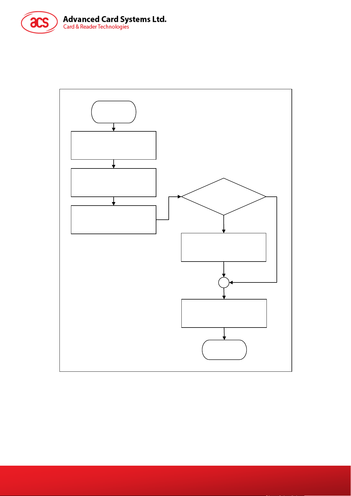
9.0. Operation Flow for PIN Verification and Modification
(PC/SC 2.0 Part 10)
ACR83 reader supports PC/SC 2.0 Part 10. The flowchart below shows the PIN verification and
modification operation.
START
Connect to ACR83
(SCardConnect)
Get Feature Request
(SCardControl)
Modify the
Verify PIN Direct
(SCardControl)
Modify PIN Direct
(SCardControl)
Disconnect ACR83
(SCardDisconnect)
Figure 1: PIN Verification and Modification Operation Flowchart
Yes
In order to use PIN verification and modification, the SCardControl API must be called with Get
Feature Request control code. This API will return a list of supported features from the reader.
In ACR83, only Verify PIN Direct, Modify PIN Direct and IFD PIN Properties are supported. To use
these features, you can get the control codes from the list. For more information, please refer to
PC/SC 2.0 Specification Part 10.
Page 13 of 49
ACR83 – Reference Manual info@acs.com.hk
Version 1.05
www.acs.com.hk
Page 14

10.0. CCID SPE Data Structure
The ACR83 SPE is based on the CCID SPE which is fully compatible to CCOD SPE.
If the application program uses the CCID SPE, it must use the CCID PC_to_RDR_Secure to send the
APDU.
According to CCID specification, the SPE has two modes:
1. PIN Verification
2. PIN Modification
The Modes setting is based on CCID abPINOperationDataStructure (Please refer to CCID
specification 6.1.11.1).
bPINOperation:
00h: PIN Verification
01h: PIN Modification
Any other values will not be supported by ACR83.
Page 14 of 49
ACR83 – Reference Manual info@acs.com.hk
Version 1.05
www.acs.com.hk
Page 15

11.0. PIN Verification Data Structure
For PIN Verification, we need to understand the PIN Verification Data Structure.
bTimeOut: Number of seconds for key press (00h: default value = 60 seconds)
abPINApdu = CLA INS P1 P2 Lc XX XX XX XX …
Example: abPINApdu = 00 20 00 01 08 FF FF FF FF FF FF FF FFh
bmFormatString (Bit 7):
0h: means the system units is bit
1h: means the system units is byte
Bit 6~3 (SpePinPos): PIN position after format in the APDU command
Bit2 (SpeLeftRight): 0=Left, 1=Right
Bit1~0 (SpePINTyp):
00h: Binary ex: 01 02 03 04 05 06
01h: BCD ex: 12 34 56
10h: ASCII ex: 31 32 33 34 35 36
bmPINBlockString:
Bit7~4 (SpePINSize):
Ex: 2 means 2*2 -1 = 4 - 1 allow maximum 3 digits PIN
If SpePINSize = 0, it means no PIN management.
Bit3~0 (SpePINLen): PIN block size in bytes after justification and formatting
bmPINLengthFormat:
Bit3~0 (SpePINLenPos): Indicate the PIN length position in the APDU command
If SpePINLenPos =0, it means no PIN management.
Bit4: 0: indicates if the SpePINLenPos is in bit or byte unit
wPINMaxExtraDigit:
XX: (SpePinMin) Minimum PIN Size
YY: (SpePinMax) Maximum PIN Size
bNumberMessage:
00h: No message display in LCD
01h: Display one message: LCD will display “Enter PIN:”
FFh: Default value equal to 01h
Page 15 of 49
ACR83 – Reference Manual info@acs.com.hk
Version 1.05
www.acs.com.hk
Page 16

bMsgIndex:
00h: LCD will display “Enter PIN:”
Any other values will raise an error.
If the data structure format error, the ACR83 will give “6B 80h.”
For the system unit is bit (bmFormatString bit 7=0). The APDU formatting is total different with system
unit is byte (bmFormatString bit 7=1).
11.1. Error Checking (Bit)
Verification system unit is bit.
Command Header
APDU Command
Header
CLA INS P1 P2 Lc
Check points in implementing the PIN Verification Data Structure:
• SpePINLen must be equal to Lc
• SpePINPos must be equal or larger than SpePINLenPos + SpePINSize
• SpePINLen – SpePINPos must be larger or equal to SpePinMax (if BCD, need multiple 4)
• SpePinMax must be equal or larger than SpePinMin
• SpePinMax cannot be larger than 16 digits because LCD one row only have 16 digits
• SpePinMin must be equal or larger than 1
APDU
Length
Offset SpePINPos PIN
Offset
SpePINLenPos
SpePINLen
SpePINSize
Not used
field/may not exist
11.2. Error Checking (Byte)
Check points in implementing the PIN Verification Data Structure:
• Lc must equal to SpePINLen + SpePINPos
• SpePINPos must be equal or larger than SpePINLenPos + SpePINSize
PIN
• SpePINLen – SpePINPos must be larger or equal to SpePinMax (if BCD, need multiple 4)
• SpePinMax must be equal or larger than SpePinMin
• SpePinMax cannot be larger than 16 digits because LCD one row only have 16 digits
• SpePinMin must be equal or larger than 1
Verification system unit is byte.
Command Header Offset SpePINPos
APDU Command
Header
CLA INS P1 P2
APDU
Length
Lc
Offset SpePINPos PIN
Offset
SpePINLenPos
SpePINSize
Not used
field
SpePINLen
PIN
Page 16 of 49
ACR83 – Reference Manual info@acs.com.hk
Version 1.05
www.acs.com.hk
Page 17

11.3. Verification Example 1
System unit is bit.
Command Header
APDU Command
Header
CLA INS P1 P2 Lc
Check points in implementing the PIN Verification Data Structure:
• SpePINLen must be equal to Lc
• SpePINPos must be equal or larger than SpePINLenPos + SpePINSize
• SpePINLen – SpePINPos must be larger or equal to SpePinMax (if BCD, need multiple 4)
• SpePinMax must be equal or larger than SpePinMin
• SpePinMax cannot be larger than 16 digits because LCD one row only have 16 digits
• SpePinMin must be equal or larger than 1
abPINApdu = 00 20 00 01 09 57 30 30 30 30 30 30 30 30h
After Lc (09h), the first 7 bits (0101011) is control character.
APDU
Length
Offset SpePINPos PIN
Offset
SpePINLenPos
SpePINLen
SpePINSize
Not used
field/may not exist
PIN
bmFormatString=39h
SpePinPos=7 bits because bmFormatString bit 7 = 0
SpeLeftRight=Left
SpePINTyp=BCD
bmPINBlockString=49h
SpePINSize=4 bits
SpePINLen=9 bytes
bmPINLengthFormat=02h
SpePINLenPos=2 bits
wPINMaxExtraDigit=010Ah
SpePinMax=0Ah
SpePinMin=01h
PIN Input = 1 2 3 4 5 6 7 8 0
Error checks points:
• Point 1: SpePINLen (9h) equal to Lc (9h)
Page 17 of 49
ACR83 – Reference Manual info@acs.com.hk
Version 1.05
www.acs.com.hk
Page 18

• Point 2: SpePINPos (7 bits) >= SpePinLenPos (2 bits) + SpePINSize (4 bits)
• Point 3: SpePINLen (9h) – SpePinPos (7 bits)[act as 1 byte] >=[SpePinMax (0Ah) * 4bits
(BCD)] = 5 bytes
: 8 bytes >=5 bytes
• Point 4: SpePinMax (0Ah) > SpePinMin (01h)
• Point 5: SpePinMax (0Ah)< =10h
• Point 6: SpePinMin (01h) >= 01h
Command Header
APDU Command
Header
00 20 00 01 09 Offset 2bits
00 20 00 01 09 01 Input 9 digits Offset 6 bit relative to Lc PIN
00 20 00 01 09 01=0101011 1001 (bits) 1 (bit)=0101011 PIN
00 20 00 01 09 0110011 (1001 replace original 0101011) PIN
How about the PIN management?
Because it is Left and BCD arrangement.
Original
Input 12 34 56 78 0
(change to bit format)
Original
APDU
Length
Offset SpePINPos 7 bits PIN
SpePINSize (4
bits)
1 0011 0000 0011 0000 0011 0000 0011 0000 0011 0000
0011 0000 0011 0000 1100 0000
0001 0010 0011 0100 0101 0110 0111 1000 0000
1 0011 0000 0011 0000 0011 0000 0011 0000 0011 0000
0011 0000 0011 0000 1100 0000
SpePINLen
Not used field/may not
exist
PIN (bits)
PIN
Input PIN 0 0010 0100 0110 1000 1010 1100 1111 0000 000
Result PIN
Result APDU in bit format
Result APDU in byte
format
The whole APDU in byte format will be:
00 20 00 01 09 66 24 68 AC F0 10 30 30 30h
If arrangement is Right:
bmFormatString change to=3Dh
00 20 00 01 09 67 30 30 30 31 23 45 67 80h
0 0010 0100 0110 1000 1010 1100 1111 0000 0001 0000
0011 0000 0011 0000 1100 0000
0110 0110 0010 0100 0110 1000 1010 1100 1111 0000 0001
0000 0011 0000 0011 0000 0011 0000
66 24 68 ac f0 10 30 30 30
Page 18 of 49
ACR83 – Reference Manual info@acs.com.hk
Version 1.05
www.acs.com.hk
Page 19

11.4. Verification Example 2
System unit is bit.
abPINApdu = 00 20 00 01 08 57 A5 30 30 30 30 30 30h
After Lc (08h), the first 11 bits (01010111 101) is control character.
bmFormatString=59h
SpePinPos=11 bits because bmFormatString bit 7 = 0
SpeLeftRight=Left
SpePINTyp=BCD
bmPINBlockString=48h
SpePINSize=4 bits
SpePINLen=8 bytes
bmPINLengthFormat=06h
SpePINLenPos=6 bits
wPINMaxExtraDigit=0108h
SpePinMax=08h
SpePinMin=01h
PIN Input = 1 2 3 4 5
Command Header
APDU Command
Header
00 20 00 01 08 Offset 6 bits
00 20 00 01 08
00 20 00 01 08
00 20 00 01 08 01010101 011 (0101 replace original 01010111 101) PIN
How about the the PIN management?
Because it is Left and BCD arrangement.
APDU
Length
01010111
101
010101
Offset SpePINPos 7 bits PIN
SpePINSize
Input 5 digits
0101 (bits) 1 (bit)= 01010111 101 PIN
(4bits)
SpePINLen
Not used field/may not
exist
Offset 6 bit relative to
Lc
PIN
PIN
Original
Input 12 34 5 (change to
bit format)
Original
0 0101 0011 0000 0011 0000 0011 0000 0011 0000 0011
0000 0011 0000
0001 0010 0011 0100 0101
0 0101 0011 0000 0011 0000 0011 0000 0011 0000 0011
0000 0011 0000
PIN (bits)
Page 19 of 49
ACR83 – Reference Manual info@acs.com.hk
Version 1.05
www.acs.com.hk
Page 20

PIN (bits)
Input PIN 0 0010 0100 0110 1000 101
Result PIN
Result APDU in bit format
Result APDU in byte
format
The whole APDU in byte format will be:
00 20 00 01 08 55 62 46 8A 30 30 30 30h
If arrangement is Right:
bmFormatString change to=5Dh
00 20 00 01 08 55 65 30 30 30 31 23 45h
0 0010 0100 0110 1000 1010 0011 0000 0011 0000 0011
0000 0011 0000
0101 0101 0110 0010 0100 0110 1000 1010 0011 0000 0011
0000 0011 0000 0011 0000
55 62 46 8A 30 30 30 30
11.5. Verification Example 3
System unit is Byte.
Command Header Offset SpePINPos
APDU
Command
Header
APDU
Length
SpePINLen
Offset SpePINPos PIN
CLA INS P1 P2 Lc
Check points in implementing the PIN Verification Data Structure:
• Lc must be equal to SpePINLen + SpePINPos
• SpePINPos must be equal or larger than SpePINLenPos + SpePINSize
• SpePINLen – SpePINPos must be larger or equal to SpePinMax(if BCD, need multiple 4)
• SpePinMax must be equal or larger than SpePinMin
• SpePinMax cannot be larger than 16 digits because LCD one row only have 16 digits
• SpePinMin must be equal or larger than 1
Example1:
abPINApdu = 00 20 00 01 09 57 30 30 30 30 30 30 30 30h
After Lc (09h), the first 1 byte 57h is control character.
bmFormatString=89h
SpePinPos=1 byte because bmFormatString bit 7 = 1
Offset
SpePINLenPos
SpePINSize
Not used
field
PIN
SpeLeftRight=Left
SpePINTyp=BCD
Page 20 of 49
ACR83 – Reference Manual info@acs.com.hk
Version 1.05
www.acs.com.hk
Page 21

bmPINBlockString=48h
SpePINSize=4 bits
SpePINLen=8 bytes
bmPINLengthFormat=04h
SpePINLenPos=4 bits
wPINMaxExtraDigit=010ah
SpePinMax=0ah
SpePinMin=01h
PIN Input = 1 2 3 4 5 6 7 8 0
• Point 1: SpePINLen (9) equal to SpePINLen (8) + SpePinPos (1)
• Point 2: SpePINPos (1 Byte) >= SpePinLenPos (4 bits) + SpePINSize (4 bits)
• Point 3: SpePINLen (9) – SpePinPos (1 Byte) >=[SpePinMax (0Ah) * 4bits(BCD)] = 5 Bytes
: 8 Bytes >=5 Bytes
• Point 4: SpePinMax (0Ah) > SpePinMin (01h)
• Point 5: SpePinMax (0Ah) < =10h
• Point 6: SpePinMin (01h) >= 01h
Command Header
APDU Command
Header
00 20 00 01 09 Offset (4 bits) SpePINSize (4 bits)
00 20 00 01 09 57h Input 9 digits
00 20 00 01 09 0101=01010111 1001 (bits)
00 20 00 01 09
Lc
01011001 (59h) (1001 replace original
Offset SpePINPos (1 Byte) PIN
SpePINPos SpePINLen
Not used
field
Does not
exist
Does not
exist
01010111)
PIN
PIN
PIN
PIN
How about the PIN management?
Because it is Left and BCD arrangement
Original 00 20 00 01 09 57 30 30 30 30 30 30 30 30
Input 12 34 56 78 0
Result PIN 00 20 00 01 09 59 12 34 56 78 00 30 30 30
PIN (Byte)
Page 21 of 49
ACR83 – Reference Manual info@acs.com.hk
Version 1.05
www.acs.com.hk
Page 22

The whole APDU in byte format will be:
00 20 00 01 09 59 12 34 56 78 00 30 30 30h
If arrangement is Right:
bmFormatString change to=8Dh
00 20 00 01 08 59 30 30 30 31 23 45 67 80h
Page 22 of 49
ACR83 – Reference Manual info@acs.com.hk
Version 1.05
www.acs.com.hk
Page 23

12.0. PIN Modification Data Structure
For PIN Modification, we need to understand the PIN Modification Data Structure.
bTimeOut: Number of seconds for key press (00h: default value = 60 seconds)
abPINApdu = CLA INS P1 P2 Lc XX XX XX XXh …
For bConfirmPIN bit1 =0
Ex: abPINApdu = 00 24 00 01 08 FF FF FF FF FF FF FF FFh
(New PIN)
For bConfirmPIN bit1 =1
Ex: abPINApdu = 00 24 00 01 10 20 FF FF FF FF FF FF FF 20 FF FF FF FF FF FF FFh
(Old/Current PIN) (New PIN)
bmFormatString (Bit 7):
0: means the system units is bit
1: means the system units is byte
Bit 6~3 (SpePinPos): PIN position after format in the APDU command
Bit2 (SpeLeftRight): 0=Left, 1=Right
Bit1~0 (SpePINTyp):
00h: Binary ex: 01 02 03 04 05 06
01h: BCD ex: 12 34 56
10h: ASCII ex: 31 32 33 34 35 36
bmPINBlockString:
Bit7~4 (SpePINSize):
Ex: 2 means 2*2 -1 = 4 - 1 allow maximum 3 digits PIN
If SpePINSize = 0, it means no PIN management.
Bit3~0 (SpePINLen): PIN block size in bytes after justification and formatting
bmPINLengthFormat:
Bit3~0 (SpePINLenPos): indicates the PIN length position in the APDU command
If SpePINLenPos =0, it means no PIN management.
Bit4: 0: indicates if the SpePINLenPos is in bit or byte unit
bInsertionOffsetOld (SpeOffsetOld): insertion position offset in byte for the current PIN
bInsertionOffsetNew (SpeOffsetNew): insertion position offset in byte for the new PIN
Page 23 of 49
ACR83 – Reference Manual info@acs.com.hk
Version 1.05
www.acs.com.hk
Page 24

bConfirmPIN:
Bit 0: 0=no confirmation of New PIN request 1: Confirmation of New PIN request
Bit 1: 0=no Old (current) PIN entry request 2: Old (current) PIN entry request
00h: bNumberMessage must be equal to 00h or 01h
01h: bNumberMessage must be equal to 02h
02h: bNumberMessage must be equal to 02h
03h: bNumberMessage must be equal to 03h
Otherwise, it will raise an error.
wPINMaxExtraDigit:
XX: (SpePinMin) Minimum PIN Size
YY: (SpePinMax) Maximum PIN Size
bMsgIndex1:
00h: LCD will display “Enter PIN:”
Any other values will raise an error.
bMsgIndex2:
01h: LCD will display “Enter New PIN:”
Any other values will raise an error.
bMsgIndex3:
02h: LCD will display “Enter Confirm PIN:”
Any other values will raise an error.
12.1. Modification (Bit) bConfirmPIN Bit1=0
Modification bConfirmPIN Bit1 = 0
(No current/Old PIN entry requested)
System unit is bit.
APDU Command
APDU Header
CLA INS P1 P2 Lc
APDU
Lc
SpeOffsetNew SpePINLen
Maybe not Offset SpePINPos PIN
Exists
Offset
SpePINLenPos
SpePINSize
Not used
field/Does not
exist
PIN
12.2. Modification (Bit) bConfirmPIN Bit1=0 Data Structure Error
Checking
Check points in implementing the PIN Modification Data Structure:
• SpePINLen + SpeOffsetNew must be equal to Lc
Page 24 of 49
ACR83 – Reference Manual info@acs.com.hk
Version 1.05
www.acs.com.hk
Page 25

• SpePINPos must be equal or larger than SpePINLenPos + SpePINSize
• SpePINLen – SpePINPos must be larger or equal to SpePinMax(if BCD, need multiple 4)
• SpePinMax must be equal or larger than SpePinMin
• SpePinMax cannot be larger than 16 digits because LCD one row only have 16 digits
• SpePinMin must be equal or larger than 1
12.3. Modification (Byte) bConfirmPIN Bit1=0
Modification bConfirmPIN Bit1 = 0
(No current/Old PIN entry requested)
System unit is byte.
Command Header
APDU
Command
Header
CLA INS P1
P2
APDU
Lc
Lc
OffsetNew
OffsetNew Offset SpePINPos PIN
OffsetNew
SpePINLenPos
Offset SpePINPos
Offset
SpePINSize
Not used
field
SpePINLen
PIN
12.4. Modification (Byte) bConfirmPIN Bit1=0 Data Structure Error
Checking
Check points in implementing the PIN Modification Data Structure:
• Lc must be equal to SpePINLen + SpePINPos + SpeOffsetNew
• SpePINPos must be equal or larger than SpePINLenPos + SpePINSize
• SpePINLen – SpePINPos must be larger or equal to SpePinMax(if BCD, need multiple 4)
• SpePinMax must be equal or larger than SpePinMin
• SpePinMax cannot be larger than 16 digits because LCD one row only have 16 digits
• SpePinMin must be equal or larger than 1
12.5. Modification (Bit) bConfirmPIN Bit1=1
bConfirmPIN Bit1 = 1
(Current/Old PIN entry requested)
System unit is bit.
APDU Command
APDU
Header
CLA INS
P1 P2
APDU
Lc
Lc
SpeOffsetOld SpePINLen
Maybe not Offset SpePINPos Old PIN
Exist
Offset
SpePINLenPos
SpePINSize
Not used
field
Old PIN
Page 25 of 49
ACR83 – Reference Manual info@acs.com.hk
Version 1.05
www.acs.com.hk
Page 26

SpeOffsetNew
Maybe not Offset SpePINPos New PIN
Exist
Offset
SpePINLenPos
SpePINSize
SpePINLen
Not used field New PIN
12.6. Modification (Bit) bConfirmPIN Bit1=1 Data Structure Error
Checking
Check points in implementing the PIN Modification Data Structure:
• SpePINLen + SpeOffsetNew must equal to Lc
• SpeOffsetNew >= SpeOffsetOld + SpePINLen
• SpePINPos must be equal or larger than SpePINLenPos + SpePINSize
• SpePINLen – SpePINPos must be larger or equal to SpePinMax (if BCD, need multiple 4)
• SpePinMax must be equal or larger than SpePinMin
• SpePinMax cannot be larger than 16 digits because LCD one row only have 16 digits
• PinMin must be equal or larger than 1
12.7. Modification (Byte) bConfirmPIN Bit1=1
bConfirmPIN Bit1 = 1
(Current/Old PIN entry requested)
System unit is byte.
APDU Command
APDU Header
CLA INS P1 P2 Lc
SpeOffsetNew
Maybe not Offset SpePINPos New PIN
Exists
APDU
Lc
SpeOffsetOld
Maybe not Offset SpePINPos Old PIN
Exist
Offset SpePINPos
Offset
SpePINLenPos
Offset
SpePINLenPos
SpePINSize
Offset SpePINPos
SpePINSize
Not used field New PIN
Not used
field
SpePINLen
SpePINLe
n
Old PIN
12.8. Modification (Byte) bConfirmPIN Bit1=1 Data Structure Error
Checking
Check points in implementing the PIN Modification Data Structure:
• SpePINLen + SpeOffsetNew + SpePINPos must equal to Lc
• SpeOffsetNew >= SpeOffsetOld + SpePINPos + SpePINLen
• SpePINPos must be equal or larger than SpePINLenPos + SpePINSize
Page 26 of 49
ACR83 – Reference Manual info@acs.com.hk
Version 1.05
www.acs.com.hk
Page 27

• SpePINLen – SpePINPos must be larger or equal to SpePinMax(if BCD, need multiple 4)
• SpePinMax must be equal or larger than SpePinMin
• SpePinMax cannot be larger than 16 digits because LCD one row only have 16 digits
• SpePinMin must be equal or larger than 1
12.9. Modification Example 1
Modification bConfirmPIN Bit1 = 0
(No current/Old PIN entry requested)
System unit is bit.
APDU Command
APDU Header
CLA INS P1 P2 Lc
Check points in implementing the PIN Modification Data Structure:
• SpePINLen + SpeOffsetNew must be equal to Lc
• SpePINPos must be equal or larger than SpePINLenPos + SpePINSize
• SpePINLen – SpePINPos must be larger or equal to SpePinMax(if BCD, need multiple 4)
• SpePinMax must be equal or larger than SpePinMin
• SpePinMax cannot be larger than 16 digits because LCD one row only have 16 digits
• SpePinMin must be equal or larger than 1
abPINApdu = 00 24 00 01 0A 20 57 30 30 30 30 30 30 30 30h
bConfirmPIN = 00h (if bConfirmPIN = 00h, the bNumberMessage must equal to 01h, 00h)
APDU
Lc
SpeOffsetNew SpePINLen
Maybe not Offset SpePINPos PIN
Exists
Offset
SpePINLenPos
SpePINSize
Not used field/Does
not exist
PIN
Enter the New PIN once.
bmFormatString=39h
SpePinPos=7 bits because bmFormatString bit 7 = 0
SpeLeftRight=Left
SpePINTyp=BCD
bmPINBlockString=49h
SpePINSize=4 bits
SpePINLen=9 bytes
bmPINLengthFormat=02h
SpePINLenPos=2 bits
Page 27 of 49
ACR83 – Reference Manual info@acs.com.hk
Version 1.05
www.acs.com.hk
Page 28

wPINMaxExtraDigit=010Ah
SpePinMax=0Ah
SpePinMin=0Ah
bInsertionOffsetNew(SpeOffsetNew)=01h
SpeOffsetNew =1 byte
bNumberMessage=01h
Show “Enter New PIN:”
If bNumberMessage=00h
No message will be shown, but user needs to input the PIN.
New PIN Input = 1 2 3 4 5 6 7 8 0
• Point 1: Lc (0A) equal to SpePINLen (09) + SpeOffsetNew (01h)
• Point 2: SpePINPos (7 bits) >= SpePinLenPos (2 bits) + SpePINSize (4 bits)
• Point 3: SpePINLen (9) – SpePinPos (7 bits)[act as 1 byte] >=[SpePinMax (0Ah) *
4bits(BCD)] = 5 bytes
: 8 bytes >=5 bytes
• Point 4: SpePinMax (0Ah) > SpePinMin (01h)
• Point 5: SpePinMax (0Ah) < =10h
• Point 6: SpePinMin (01h) >= 01h
Command Header
APDU Header
00 24 00 01 09 Offset Offset (2 bits)
00 24 00 01 09 1 byte 01 Input 9 digits
00 24 00 01 09 20 01=0101011 1001 (bits) 1 (bit)=0101011 PIN
00 24 00 01 09 20 0110011 (1001 replace original 0101011) PIN
APDU
Lc
OffsetNew SpePINLen
OffsetNew
Offset SpePINPos 7 bits PIN
SpePINSize (4
bits)
Not used field/Does not
Offset 6 bit relative to
exist
Lc
PIN
PIN
How about the PIN management?
Because it is Left and BCD arrangement.
Original
Input 12 34 56 78 0
(change to bit format)
1 0011 0000 0011 0000 0011 0000 0011 0000 0011 0000
0011 0000 0011 0000 1100 0000
0001 0010 0011 0100 0101 0110 0111 1000 0000
PIN (bits)
Page 28 of 49
ACR83 – Reference Manual info@acs.com.hk
Version 1.05
www.acs.com.hk
Page 29

PIN (bits)
Original
Input New PIN 0 0010 0100 0110 1000 1010 1100 1111 0000 000
Result PIN
Result APDU in bit
format
Result APDU in byte
format
The whole APDU in byte format will be:
00 24 00 01 0A 20 66 24 68 ac f0 10 30 30 30h
If arrangement is Right:
bmFormatString change to=3Dh
00 24 00 01 0A 20 67 30 30 30 31 23 45 67 80h
If SpeOffsetNew = 00h and abPINApdu = 00 24 00 01 09 57 30 30 30 30 30 30 30 30h
bmFormatString change to=39h
1 0011 0000 0011 0000 0011 0000 0011 0000 0011 0000
0011 0000 0011 0000 1100 0000
0 0010 0100 0110 1000 1010 1100 1111 0000 0001 0000
0011 0000 0011 0000 1100 0000
0110 0110 0010 0100 0110 1000 1010 1100 1111 0000 0001
0000 0011 0000 0011 0000 0011 0000
66 24 68 ac f0 10 30 30 30
The result formatting APDU = 00 24 00 01 09 66 24 68 AC F0 10 30 30 30h
12.10. Modification Example 2
It is the same as example 1, only bConfirmPIN is changed to 01h.
abPINApdu = 00 24 00 01 0A 20 57 30 30 30 30 30 30 30 30h
bConfirmPIN = 01h (If bConfirmPIN=01h, bNumberMessage must equal to 02h)
Enter the New PIN and confirm the New PIN.
bmFormatString=39h
SpePinPos=7 bits because bmFormatString bit 7 = 0
SpeLeftRight=Left
SpePINTyp=BCD
bmPINBlockString=49h
SpePINSize=4 bits
SpePINLen=9 bytes
bmPINLengthFormat=02h
SpePINLenPos=2 bits
Page 29 of 49
ACR83 – Reference Manual info@acs.com.hk
Version 1.05
www.acs.com.hk
Page 30

wPINMaxExtraDigit=010Ah
SpePinMax=0Ah
SpePinMin=01h
bInsertionOffsetNew (SpeOffsetNew)=01h
SpeOffsetNew =1 byte
bNumberMessage=02h
Show “Enter New PIN:” and
Show “Enter Confirm PIN”
New PIN Input = 1 2 3 4 5 6 7 8 0
• Point 1: Lc (0Ah) equal to SpePINLen (09) + SpeOffsetNew (01h)
• Point 2: SpePINPos (7 bits) >= SpePinLenPos (2 bits) + SpePINSize (4 bits)
• Point 3: SpePINLen (9) – SpePinPos (7 bits) [act as 1 byte] >= [SpePinMax (0Ah) *
4bits(BCD)] = 5 bytes
: 8 bytes >=5 bytes
• Point 4: SpePinMax (0Ah) > SpePinMin (01h)
• Point 5: SpePinMax (0Ah) < 10h
• Point 6: SpePinMin (01h) >= 01h
Command Header
APDU
Header
00 24 00 01 09 Offset Offset (2 bits)
00 24 00 01 09 1 byte 01 Input 9 digits
00 24 00 01 09 20 01=0101011 1001(bits) 1 (bit)=0101011 PIN
00 24 00 01 09 20 0110011 (1001 replace original 0101011) PIN
APDU
Lc
OffsetNew SpePINLen
OffsetNew
Offset SpePINPos 7 bits PIN
SpePINSize
(4 bits)
Not used
field/Does not
exist
Offset 6 bit
relative to Lc
PIN
PIN
How about the PIN management?
Because it is Left and BCD arrangement.
Original
Input 12 34 56 78 0
(change to bit format)
1 0011 0000 0011 0000 0011 0000 0011 0000 0011 0000
0011 0000 0011 0000 1100 0000
0001 0010 0011 0100 0101 0110 0111 1000 0000
PIN (bits)
Page 30 of 49
ACR83 – Reference Manual info@acs.com.hk
Version 1.05
www.acs.com.hk
Page 31

PIN (bits)
Original
Input New PIN 0 0010 0100 0110 1000 1010 1100 1111 0000 000
Result PIN
Result APDU in bit
format
Result APDU in byte
format
The whole APDU in byte format will be:
00 24 00 01 0A 20 66 24 68 ac f0 10 30 30 30h
If arrangement is Right:
bmFormatString change to=3Dh
00 24 00 01 0A 20 67 30 30 30 31 23 45 67 80h
If SpeOffsetNew = 00h and abPINApdu = 00 24 00 01 09 57 30 30 30 30 30 30 30 30h
bmFormatString change to=39h
1 0011 0000 0011 0000 0011 0000 0011 0000 0011 0000
0011 0000 0011 0000 1100 0000
0 0010 0100 0110 1000 1010 1100 1111 0000 0001 0000
0011 0000 0011 0000 1100 0000
0110 0110 0010 0100 0110 1000 1010 1100 1111 0000 0001
0000 0011 0000 0011 0000 0011 0000
66 24 68 AC F0 10 30 30 30
The result formatting APDU = 00 24 00 01 09 66 24 68 ac f0 10 30 30 30h
12.11. Modification Example 3
bConfirmPIN Bit1 = 0
(No current/Old PIN entry requested)
System unit is Byte.
Command Header
APDU
Command
Header
CLA INS P1 P2 Lc OffsetNew
Check points in implementing the PIN Modification Data Structure:
1. Lc must be equal to SpePINLen + SpePINPos + SpeOffsetNew
2. SpePINPos must be equal or larger than SpePINLenPos + SpePINSize
3. SpePINLen – SpePINPos must be larger or equal to SpePinMax (if BCD, need multiple 4)
APDU
Lc
OffsetNew
OffsetNew
Offset
SpePINLenPos
Offset SpePINPos
Offset SpePINPos PIN
SpePINSize
Not used
field
SpePINLen
PIN
4. SpePinMax must be equal or larger than SpePinMin
5. SpePinMax cannot be larger than 16 digits because LCD one row only have 16 digits
6. SpePinMin must be equal or larger than 1
Page 31 of 49
ACR83 – Reference Manual info@acs.com.hk
Version 1.05
www.acs.com.hk
Page 32

abPINApdu = 00 24 00 01 09 57 30 30 30 30 30 30 30 30h
After Lc (09h), the first 1 byte 57h is control character
bConfirmPIN = 01h (If bConfirmPIN=01h, bNumberMessage must equal to 02h)
Enter the New Pin and confirm the New Pin
bmFormatString=89h
SpePinPos=1 byte because bmFormatString bit 7 = 1
SpeLeftRight=Left
SpePINTyp=BCD
bmPINBlockString=48h
SpePINSize=4 bits
SpePINLen=8 bytes
bmPINLengthFormat=04h
SpePINLenPos=4 bits
wPINMaxExtraDigit=010Ah
SpePinMax=0Ah
SpePinMin=01h
bInsertionOffsetNew (SpeOffsetNew)=00h
SpeOffsetNew =00 byte
bNumberMessage=02h
Show “Enter New PIN:” and
Show “Enter Confirm PIN”
PIN Input = 1 2 3 4 5 6 7 8 0
• Point 1: Lc (9) equal to SpeOffsetNew (0) + SpePINLen (8) + SpePinPos (1)
• Point 2: SpePINPos (1 Byte) >= SpePinLenPos (4 bits) + SpePINSize (4 bits)
• Point 3: SpePINLen (9) – SpePinPos (1 Byte) >=[SpePinMax (0Ah) * 4 bits(BCD)] = 5 bytes
: 8 bytes >=5 bytes
• Point 4: SpePinMax (0Ah) > SpePinMin (01h)
• Point 5: SpePinMax (0Ah) < =10h
• Point 6: SpePinMin (01h) >= 01h
Page 32 of 49
ACR83 – Reference Manual info@acs.com.hk
Version 1.05
www.acs.com.hk
Page 33

Command Header
APDU Command
Header
00 24 00 01 09 Offset (4 bits) SpePINSize (4bits)
00 24 00 01 09 57h Input 9 digits
00 24 00 01 09 0101=01010111 1001(bits)
00 24 00 01 09
How about the PIN management?
Because it is Left and BCD arrangement
Lc
01011001 (59h) (1001 replace original
Original 00 24 00 01 09 57 30 30 30 30 30 30 30 30h
Input 12 34 56 78 0h
Result PIN 00 24 00 01 09 59 12 34 56 78 00 30 30 30h
SpePINPos SpePINLen
Offset SpePINPos 1 Byte PIN
01010111)
PIN (Byte)
Not used
field
Does not
exist
Does not
exist
- PIN
PIN
PIN
PIN
The whole APDU in byte format will be:
00 24 00 01 09 59 12 34 56 78 00 30 30 30h
If arrangement is Right:
bmFormatString change to=8Dh
00 24 00 01 08 59 30 30 30 31 23 45 67 80h
12.12. Modification Example 4
bConfirmPIN Bit1 = 1
(Current/Old PIN entry requested)
System unit is bit.
APDU Command
APDU Header
CLA INS P1 P2 Lc
APDU
Lc
SpeOffsetOld SpePINLen
Maybe not Offset SpePINPos Old PIN
Exists
Offset
SpePINLenPos
SpePINSize
Not used
field
Old PIN
SpeOffsetNew SpePINLen
Maybe not Offset SpePINPos New PIN
Exists
Offset
SpePINLenPos
SpePINSize
Not used field New PIN
Page 33 of 49
ACR83 – Reference Manual info@acs.com.hk
Version 1.05
www.acs.com.hk
Page 34

Check points in implementing the PIN Modification Data Structure:
• SpePINLen + SpeOffsetNew must be equal to Lc
• SpeOffsetNew > = SpeOffsetOld + SpePINLen
• SpePINPos must be equal or larger than SpePINLenPos + SpePINSize
• SpePINLen – SpePINPos must be larger or equal to SpePinMax (if BCD, need multiple 4)
• SpePinMax must be equal or larger than SpePinMin
• SpePinMax cannot be larger than 16 digits because LCD one row only have 16 digits
• SpePinMin must be equal or larger than 1
abPINApdu = 00 24 00 01 12 08 02 30 30 30 30 30 30 30 09 03 30 30 30 30 30 30 30h
bConfirmPIN = 02h (if bConfirmPIN =02h , bNumberMessage must equal to 02h)
bmFormatString=41h
SpePinPos=8 bit because bmFormatString bit 7 = 0
SpeLeftRight=Left
SpePINTyp=BCD
bmPINBlockString=48h
SpePINSize=4 bits
SpePINLen=8 bytes
bmPINLengthFormat=04h
SpePINLenPos=4 bits
wPINMaxExtraDigit=010Ah
SpePinMax=0Ah
SpePinMin=01h
bInsertionOffsetNew(SpeOffsetNew)=0Ah
SpeOffsetNew =0Ah byte
bInsertionOffsetOld (SpeOffsetOld)=01h
SpeOffsetOld =01h byte
PIN Input (Old/Current PIN) = 1 2 3 4 5 6
PIN Input (New PIN) = 1 2 3 4 5 6 7 8 9 0
bNumberMessage=02h
Page 34 of 49
ACR83 – Reference Manual info@acs.com.hk
Version 1.05
www.acs.com.hk
Page 35

Show “Enter PIN:” means enter the old/current PIN and
Show “Enter New PIN”
• Point 1: Lc (12h) equal to SpeOffsetNew (0Ah) + SpePINLen (8)
• Point 2: SpeOffsetNew (0Ah) >= SpeOffsetOld (1) + SpePINLen (8)
• Point 3: SpePINPos (8 bits) >= SpePinLenPos (4 bits) + SpePINSize (4 bits)
• Point 4: SpePINLen (8) – SpePinPos (4 bits) >=[SpePinMax (0Ah) * 4bits(BCD)] = 5 bytes
: 7.5 bytes >=5 bytes
• Point 5: SpePinMax (0Ah) > SpePinMin (01h)
• Point 6: SpePinMax (0Ah) < =10h
• Point 7: SpePinMin (01h) > = 01h
Command Header
APDU
Header
00 24 00 01 12 Offset Offset (4 bits) SpePINSize (4 bits)
00 24 00 01 12 1 byte 02 Input 6 digits -
00 24 00 01 12 08 0000=00000010 0110 (bits) -
00 24 00 01 12 08
OffsetNew SpePINLen
OffsetNew
Offset Offset (4 bits) SpePINSize (4 bits)
0A bytes 03 Input 10 digits - New PIN
relative to Lc 00=00000011 1010 (bits) - New PIN
APDU
Lc
OffsetOld SpePINLen
OffsetOld
Offset SpePINPos 8 bits = 1byte New PIN
Offset SpePINPos 8 bits = 1byte
Not
used
field
00000110 (0110 replace original
00000010)
Not used
field
-
New PIN
Old
PIN
Old
PIN
Old
PIN
Old
PIN
Old
PIN
09 00001010 (1010 replace original 00000011) - New PIN
First, handle the old PIN.
Original
Input 12 34 56
Result PIN
00 24 00 01 12 08 02 30 30 30 30 30 30 30 09 03 30 30 30 30
30 30 30
00 24 00 01 12 08 06 12 34 56 30 30 30 30 09 03 30 30 30 30
30 30 30
Old PIN (Byte)
Page 35 of 49
ACR83 – Reference Manual info@acs.com.hk
Version 1.05
www.acs.com.hk
Page 36

And then, handle the New PIN.
Original
Input 12 34 56 78 90h
Result PIN
The whole APDU after the format will be:
00 24 00 01 12 08 06 12 34 56 30 30 30 30 09 0A 12 34 56 78 90 30 30h
00 24 00 01 12 08 06 12 34 56 30 30 30 30 09 03 30 30 30 30
30 30 30h
00 24 00 01 12 08 06 12 34 56 30 30 30 30 09 0A 12 34 56 78
90 30 30h
New PIN (Byte)
12.13. Modification Example 5
BConfirmPIN Bit1 = 1
(Current/Old PIN entry requested)
System unit is byte.
APDU Command
APDU Header
CLA INS P1 P2 Lc
APDU
Lc
SpeOffsetOld
Maybe not Offset SpePINPos Old PIN
Exists
SpePINLenPos
Offset SpePINPos
Offset
SpePINSize
Not used
field
SpePINLen
Old PIN
SpeOffsetNew
Maybe not Offset SpePINPos New PIN
Exists
Check points in implementing the PIN Modification Data Structure:
• SpePINLen + SpeOffsetNew + SpePINPos must be equal to Lc
• SpeOffsetNew >= SpeOffsetOld + SpePINPos + SpePINLen
• SpePINPos must be equal or larger than SpePINLenPos + SpePINSize
• SpePINLen – SpePINPos must be larger or equal to SpePinMax (if BCD, need multiple 4)
• SpePinMax must be equal or larger than SpePinMin
• SpePinMax cannot be larger than 16 digits because LCD one row only have 16 digits
• SpePinMin must be equal or larger than 1
abPINApdu = 00 24 00 01 12 2F 0A A6 30 30 30 30 30 30 2E FB C7 30 30 30 30 30 30h
Offset
SpePINLenPos
Offset SpePINPos
SpePINSize
SpePINLen
Not used field New PIN
bConfirmPIN = 03h (if bConfirmPIN = 03h, bNumberMessage must equal to 03h or FFh)
Page 36 of 49
ACR83 – Reference Manual info@acs.com.hk
Version 1.05
www.acs.com.hk
Page 37

bmFormatString=91h
SpePinPos=2 bytes because bmFormatString bit 7 = 1
SpeLeftRight=Left
SpePINTyp=BCD
bmPINBlockString=46h
SpePINSize=4 bits
SpePINLen=6 bytes
bmPINLengthFormat=11h
SpePINLenPos=1 byte
wPINMaxExtraDigit=010Ah
SpePinMax=0Ah
SpePinMin=01h
bInsertionOffsetNew (SpeOffsetNew)=0Ah
SpeOffsetNew =0Ah byte
bInsertionOffsetOld (SpeOffsetOld)=01h
SpeOffsetOld =00h byte
PIN Input(Old/Current Pin) = 1 2 3 4 5 6
PIN Input(New Pin) = 1 2 3 4 5 6 7 8 9 0
bNumberMessage=03h or FFh
Show “Enter PIN:” means enter the old/current PIN and
Show “Enter New PIN”
Show “Confirm New PIN”
• Point 1: Lc (12h) equal to SpeOffsetNew (0Ah) + SpePINLen (6) + SpePinPos (2)
• Point 2: SpeOffsetNew (0Ah) >= SpeOffsetOld (1) + SpePINLen (6) + SpePinPos (2)
• Point 3: SpePINPos (2 Bytes) >= SpePinLenPos (1 Byte) + SpePINSize (4 bits)
• Point 4: SpePINLen (6) = [SpePinMax (0Ah) * 4bits(BCD)] = 5 bytes
: 6 bytes >=5 bytes
• Point 5: SpePinMax (0Ah) > SpePinMin (01h)
• Point 6: SpePinMax (0Ah) <=10h
• Point 7: SpePinMin (01h) >= 01h
Page 37 of 49
ACR83 – Reference Manual info@acs.com.hk
Version 1.05
www.acs.com.hk
Page 38

Command Header
APDU Header
00 24 00 01 12 Offset
00 24 00 01 12 1 byte 0A Input 6 digits 0110 Old PIN
00 24 00 01 12 2F 0A 0110 (bits) 0110 Old PIN
00 24 00 01 12 2F 0A
OffsetNew SpePINLen
OffsetNew
Offset
0A bytes FB Input 10 digits 0111 New PIN
relative to Lc FB 1010 (bits) 0111 New PIN
2E FB 1010 (1010 replace original C7) 0111 New PIN
APDU
Lc
Offset (1
OffsetOld SpePINLen
Offset SpePINPos = 2 bytes Old PIN
Offset
SpePINSize
(4 bits)
66 replace
A6
Byte)
OffsetOld
(1 Byte)
Offset SpePINPos 8 bits = 1 byte New PIN
SpePINSize (4 bits)
Not used field Old PIN
0110 Old PIN
Not used
field
New PIN
First, handle the Old PIN.
Original
Input 12 34 56
Result PIN
And then handle the New PIN.
Original
Input 12 34 56 78 90
Result PIN
The whole APDU after the format will be:
00 24 00 01 12 2F 0A A6 30 30 30 30 30 30 2E FB C7 30 30
30 30 30 30
00 24 00 01 12 2F 0A 66 12 34 56 30 30 30 2E FB C7 30 30
30 30 30 30
00 24 00 01 12 2F 0A 66 12 34 56 30 30 30 2E FB C7 30 30
30 30 30 30
00 24 00 01 12 2F 0A 66 12 34 56 30 30 30 2E FB A7 12 34
56 78 90 30
Old PIN (Byte)
New PIN (Byte)
00 24 00 01 12 2F 0A 66 12 34 56 30 30 30 2E FB A7 12 34 56 78 90 30h
Page 38 of 49
ACR83 – Reference Manual info@acs.com.hk
Version 1.05
www.acs.com.hk
Page 39

Appendix A. bmFormatString Description
Bit Number Description
The system units’ type indicator:
Bit 7
Bit 6 – 3
Bit 2
Bit 1-0
If 0h: the system units are bits
If 1h: the system units are bytes
This bit quantifies the next parameter (unit moving).
Define the PIN position after format in the APDU command (relative to the first
data after Lc). The position is based on the system units’ type indicator
(maximum 1111 for 15 system units).
Bit mask for the PIN justification:
If 0h: Left justify data
If 1h: Right justify data
Bit wise for the PIN format type:
00h: binary
01h: BCD
10h: ASCII
Page 39 of 49
ACR83 – Reference Manual info@acs.com.hk
Version 1.05
www.acs.com.hk
Page 40

Appendix B. bmPINBlockString Description
Bit Number Description
Bit 7 - 4
Bit 3 - 0
Size in bits of the PIN length inserted in the APDU command. (If 0h,
then the effective pin length is not inserted in the APDU command)
PIN length information: PIN block size in bytes after justification and
formatting
Page 40 of 49
ACR83 – Reference Manual info@acs.com.hk
Version 1.05
www.acs.com.hk
Page 41

Appendix C. bmPINLengthFormat
Bit Number Description
Bit 7-5 RFU
The system units’ type indicator:
Bit 4
If 0h: the system units are bits
If 1h: the system units are bytes
Bit 3 - 0
Indicates the PIN length position in the APDU command according to
the previous parameters (maximum 1111 for 15 system units)
Page 41 of 49
ACR83 – Reference Manual info@acs.com.hk
Version 1.05
www.acs.com.hk
Page 42

Appendix D. Sample Code (PC/SC 2.0 Part 10)
#include <stdio.h>
#include <stdlib.h>
#include <windows.h>
#include <winscard.h>
#define FEATURE_VERIFY_PIN_START 0x01
#define FEATURE_VERIFY_PIN_FINISH 0x02
#define FEATURE_MODIFY_PIN_START 0x03
#define FEATURE_MODIFY_PIN_FINISH 0x04
#define FEATURE_GET_KEY_PRESSED 0x05
#define FEATURE_VERIFY_PIN_DIRECT 0x06
#define FEATURE_MODIFY_PIN_DIRECT 0x07
#define FEATURE_MCT_READERDIRECT 0x08
#define FEATURE_MCT_UNIVERSAL 0x09
#define FEATURE_IFD_PIN_PROP 0x0A
#define FEATURE_ABORT 0x0B
#define FEATURE_SIZE (FEATURE_ABORT + 1)
#define IOCTL_SMARTCARD_GET_FIRMWARE_VERSION SCARD_CTL_CODE(2078)
#define IOCTL_SMARTCARD_DISPLAY_LCD_MESSAGE SCARD_CTL_CODE(2079)
#define IOCTL_SMARTCARD_READ_KEY SCARD_CTL_CODE(2080)
#define CM_IOCTL_GET_FEATURE_REQUEST SCARD_CTL_CODE(3400)
#pragma pack(push, 1)
typedef struct _PIN_VERIFY_STRUCTURE {
BYTE bTimeOut;
BYTE bTimeOut2;
BYTE bmFormatString;
BYTE bmPINBlockString;
BYTE bmPINLengthFormat;
USHORT wPINMaxExtraDigit;
BYTE bEntryValidationCondition;
BYTE bNumberMessage;
USHORT wLangId;
BYTE bMsgIndex;
BYTE bTeoPrologue[3];
ULONG ulDataLength;
BYTE abData[1];
} PIN_VERIFY_STRUCTURE, *PPIN_VERIFY_STRUCTURE;
typedef struct _PIN_MODIFY_STRUCTURE {
BYTE bTimeOut;
BYTE bTimeOut2;
BYTE bmFormatString;
BYTE bmPINBlockString;
BYTE bmPINLengthFormat;
BYTE bInsertionOffsetOld;
BYTE bInsertionOffsetNew;
USHORT wPINMaxExtraDigit;
BYTE bConfirmPIN;
BYTE bEntryValidationCondition;
BYTE bNumberMessage;
USHORT wLangId;
BYTE bMsgIndex1;
BYTE bMsgIndex2;
BYTE bMsgIndex3;
BYTE bTeoPrologue[3];
ULONG ulDataLength;
Page 42 of 49
ACR83 – Reference Manual info@acs.com.hk
Version 1.05
www.acs.com.hk
Page 43

BYTE abData[1];
} PIN_MODIFY_STRUCTURE, *PPIN_MODIFY_STRUCTURE;
typedef struct _PIN_PROPERTIES_STRUCTURE {
USHORT wLcdLayout;
BYTE bEntryValidationCondition;
BYTE bTimeOut2;
} PIN_PROPERTIES_STRUCTURE, *PPIN_PROPERTIES_STRUCTURE;
typedef struct _READ_KEY_OPTION {
BYTE bTimeOut;
WORD wPINMaxExtraDigit;
BYTE bKeyReturnCondition;
BYTE bEchoLCDStartPosition;
BYTE bEchoLCDMode;
} READ_KEY_OPTION;
#pragma pack(pop)
int main(int argc, char *argv[])
{
SCARDCONTEXT hSCardContext;
LONG lReturn;
lReturn = SCardEstablishContext(SCARD_SCOPE_USER, NULL, NULL,
&hSCardContext);
if (lReturn != SCARD_S_SUCCESS)
{
printf("Error: SCardEstablishContext failed with error 0x%08x\n",
lReturn);
return 1;
}
char **readerName = NULL;
int numReaders = 0;
int i;
LPTSTR pmszReaders = NULL;
LPTSTR pReader;
DWORD cch = SCARD_AUTOALLOCATE;
lReturn = SCardListReaders(hSCardContext, NULL, (LPTSTR) &pmszReaders,
&cch);
if (lReturn == SCARD_S_SUCCESS)
{
pReader = pmszReaders;
while (*pReader != '\0')
{
printf("Reader: %s\n", pReader);
// Advance to the next value
pReader = pReader + strlen(pReader) + 1;
numReaders++;
}
// Allocate reader name
readerName = new char*[numReaders];
if (readerName == NULL)
{
printf("Error: not enough memory\n");
Page 43 of 49
ACR83 – Reference Manual info@acs.com.hk
Version 1.05
www.acs.com.hk
Page 44

exit(1);
}
i = 0;
pReader = pmszReaders;
while (*pReader != '\0')
{
readerName[i] = new char[strlen(pReader) + 1];
if (readerName[i] == NULL)
{
printf("Error: not enough memory\n");
exit(1);
}
strcpy(readerName[i], pReader);
i++;
// Advance to the next value
pReader = pReader + strlen(pReader) + 1;
}
// Free the memory
SCardFreeMemory(hSCardContext, pmszReaders);
}
if (numReaders == 0)
{
printf("Error: cannot find reader in the system\n");
return 1;
}
SCARDHANDLE hCard;
DWORD dwAP;
const int BUFFER_SIZE = 300;
BYTE bSendBuffer[BUFFER_SIZE];
DWORD dwSendBufferLen;
BYTE bRecvBuffer[BUFFER_SIZE];
DWORD dwRecvBufferLen;
BYTE bOutputBuffer[100];
DWORD dwNumBytesReturned;
DWORD featureControlCodes[FEATURE_SIZE];
DWORD controlCode;
// Connect to the first reader
printf("Connecting to %s...\n", readerName[0]);
lReturn = SCardConnect(hSCardContext, readerName[0],
SCARD_SHARE_SHARED,
SCARD_PROTOCOL_T0 | SCARD_PROTOCOL_T1, &hCard, &dwAP);
if (lReturn != SCARD_S_SUCCESS)
printf("Error: SCardConnect failed with error 0x%08x\n", lReturn);
else
{
// Get feature request
printf("Getting feature request...\n");
dwRecvBufferLen = sizeof(bRecvBuffer);
lReturn = SCardControl(hCard, CM_IOCTL_GET_FEATURE_REQUEST,
NULL, 0,
bRecvBuffer, dwRecvBufferLen, &dwRecvBufferLen);
Page 44 of 49
ACR83 – Reference Manual info@acs.com.hk
Version 1.05
www.acs.com.hk
Page 45

if (lReturn != SCARD_S_SUCCESS)
printf("Error: SCardControl failed with error 0x%08x\n",
lReturn);
else
{
printf("Response: ");
for (i = 0; i < dwRecvBufferLen; i++)
printf("%02X ", bRecvBuffer[i]);
printf("\n");
memset(featureControlCodes, 0, sizeof(featureControlCodes));
i = 0;
while (i < dwRecvBufferLen)
{
// Get the feature
if ((bRecvBuffer[i] >= FEATURE_VERIFY_PIN_START) &&
(bRecvBuffer[i] <= FEATURE_ABORT))
{
// Get the TLV
if (i + 1 + 4 < dwRecvBufferLen)
{
// Get the length field
if (bRecvBuffer[i + 1] == 4)
{
controlCode = bRecvBuffer[i + 2] << 24;
controlCode |= bRecvBuffer[i + 3] << 16;
controlCode |= bRecvBuffer[i + 4] << 8;
controlCode |= bRecvBuffer[i + 5];
featureControlCodes[bRecvBuffer[i]] =
controlCode;
}
}
}
// Get the next feature
if (i + 1 < dwRecvBufferLen)
i += bRecvBuffer[i + 1] + 2;
else
break;
}
}
printf("Beginning transaction...\n");
lReturn = SCardBeginTransaction(hCard);
if (lReturn != SCARD_S_SUCCESS)
printf("Error: SCardBeginTransaction failed with error
0x%08x\n", lReturn);
// Send card command for PIN verification (ACOS3)
dwSendBufferLen = 13;
memcpy(bSendBuffer,
"\x80\x20\x06\x00\x08\xFF\xFF\xFF\xFF\xFF\xFF\xFF\xFF", dwSendBufferLen);
// Create PIN verify structure
PPIN_VERIFY_STRUCTURE pPinVerify = (PPIN_VERIFY_STRUCTURE) new
BYTE[sizeof(PIN_VERIFY_STRUCTURE) - 1 + dwSendBufferLen];
if (pPinVerify == NULL)
{
Page 45 of 49
ACR83 – Reference Manual info@acs.com.hk
Version 1.05
www.acs.com.hk
Page 46

printf("Error: not enough memory\n");
exit(1);
}
// Initialize PIN verify structure (ACOS3)
pPinVerify->bTimeOut = 0;
pPinVerify->bTimeOut2 = 0;
pPinVerify->bmFormatString = 0;
pPinVerify->bmPINBlockString = 0x08;
pPinVerify->bmPINLengthFormat = 0;
pPinVerify->wPINMaxExtraDigit = 0x0408;
pPinVerify->bEntryValidationCondition = 0x03;
pPinVerify->bNumberMessage = 0x01;
pPinVerify->wLangId = 0x0409;
pPinVerify->bMsgIndex = 0;
pPinVerify->bTeoPrologue[0] = 0;
pPinVerify->bTeoPrologue[1] = 0;
pPinVerify->bTeoPrologue[2] = 0;
pPinVerify->ulDataLength = dwSendBufferLen;
memcpy(pPinVerify->abData, bSendBuffer, dwSendBufferLen);
// Verify PIN
printf("Verifying PIN using VERIFY_PIN_DIRECT...\n");
dwRecvBufferLen = sizeof(bRecvBuffer);
featureControlCodes[FEATURE_VERIFY_PIN_DIRECT],
pPinVerify, sizeof(PIN_VERIFY_STRUCTURE) - 1 + dwSendBufferLen,
bRecvBuffer, dwRecvBufferLen, &dwRecvBufferLen);
if (lReturn != SCARD_S_SUCCESS)
printf("Error: SCardControl failed with error 0x%08x\n",
lReturn);
else
{
printf("Response: ");
for (i = 0; i < dwRecvBufferLen; i++)
printf("%02X ", bRecvBuffer[i]);
printf("\n");
}
delete [] ((BYTE*) pPinVerify);
// Send card command for PIN modification (ACOS3)
dwSendBufferLen = 13;
memcpy(bSendBuffer,
"\x80\x24\x00\x00\x08\xFF\xFF\xFF\xFF\xFF\xFF\xFF\xFF", dwSendBufferLen);
// Create PIN modify structure
PPIN_MODIFY_STRUCTURE pPinModify = (PPIN_MODIFY_STRUCTURE) new
BYTE[sizeof(PIN_MODIFY_STRUCTURE) - 1 + dwSendBufferLen];
if (pPinModify == NULL)
{
printf("Error: not enough memory\n");
exit(1);
}
// Initialize PIN modify structure (ACOS3)
pPinModify->bTimeOut = 0;
pPinModify->bTimeOut2 = 0;
pPinModify->bmFormatString = 0;
pPinModify->bmPINBlockString = 0x08;
lReturn = SCardControl(hCard,
Page 46 of 49
ACR83 – Reference Manual info@acs.com.hk
Version 1.05
www.acs.com.hk
Page 47

pPinModify->bmPINLengthFormat = 0;
pPinModify->bInsertionOffsetOld = 0;
pPinModify->bInsertionOffsetNew = 0;
pPinModify->wPINMaxExtraDigit = 0x0408;
pPinModify->bConfirmPIN = 0x01;
pPinModify->bEntryValidationCondition = 0x03;
pPinModify->bNumberMessage = 0x02;
pPinModify->wLangId = 0x0409;
pPinModify->bMsgIndex1 = 0;
pPinModify->bMsgIndex2 = 1;
pPinModify->bMsgIndex3 = 0;
pPinModify->bTeoPrologue[0] = 0;
pPinModify->bTeoPrologue[1] = 0;
pPinModify->bTeoPrologue[2] = 0;
pPinModify->ulDataLength = dwSendBufferLen;
memcpy(pPinModify->abData, bSendBuffer, dwSendBufferLen);
// Modify PIN
printf("Modifying PIN using MODIFY_PIN_DIRECT...\n");
dwRecvBufferLen = sizeof(bRecvBuffer);
lReturn = SCardControl(hCard,
featureControlCodes[FEATURE_MODIFY_PIN_DIRECT],
pPinModify, sizeof(PIN_MODIFY_STRUCTURE) - 1 + dwSendBufferLen,
bRecvBuffer, dwRecvBufferLen, &dwRecvBufferLen);
if (lReturn != SCARD_S_SUCCESS)
printf("Error: SCardControl failed with error 0x%08x\n",
lReturn);
else
{
printf("Response: ");
for (i = 0; i < dwRecvBufferLen; i++)
printf("%02X ", bRecvBuffer[i]);
printf("\n");
}
delete [] ((BYTE*) pPinModify);
printf("Ending transaction...\n");
lReturn = SCardEndTransaction(hCard, SCARD_LEAVE_CARD);
if (lReturn != SCARD_S_SUCCESS)
printf("Error: SCardEndTransaction failed with error 0x%08x\n",
lReturn);
// Get IFD PIN properties
printf("Getting IFD PIN properties...\n");
dwRecvBufferLen = sizeof(bRecvBuffer);
featureControlCodes[FEATURE_IFD_PIN_PROP],
NULL, 0,
bRecvBuffer, dwRecvBufferLen, &dwRecvBufferLen);
if (lReturn != SCARD_S_SUCCESS)
printf("Error: SCardControl failed with error 0x%08x\n",
lReturn);
else
{
printf("Response: ");
for (i = 0; i < dwRecvBufferLen; i++)
printf("%02X ", bRecvBuffer[i]);
printf("\n");
}
lReturn = SCardControl(hCard,
Page 47 of 49
ACR83 – Reference Manual info@acs.com.hk
Version 1.05
www.acs.com.hk
Page 48

// Display LCD message to ACR83
char *msg = "Hello";
printf("Displaying message (%s) to LCD...\n", msg);
lReturn = SCardControl(hCard, IOCTL_SMARTCARD_DISPLAY_LCD_MESSAGE,
msg, strlen(msg),
bOutputBuffer, sizeof(bOutputBuffer), &dwNumBytesReturned);
if (lReturn != SCARD_S_SUCCESS)
printf("Error: SCardControl failed with error 0x%08x\n",
lReturn);
else
{
// Check status
if ((dwNumBytesReturned >= 2) &&
(bOutputBuffer[0] == 0) && (bOutputBuffer[1] == 0))
printf("The message is displayed successfully\n");
else
printf("Error: cannot display LCD message\n");
}
// Read key from ACR83
READ_KEY_OPTION readKeyOption;
char keyString[100];
DWORD len;
BYTE keyReturnCondition;
// Initialize read key option
readKeyOption.bTimeOut = 0;
readKeyOption.wPINMaxExtraDigit = 0x0408;
readKeyOption.bKeyReturnCondition = 0x01;
readKeyOption.bEchoLCDStartPosition = 0;
readKeyOption.bEchoLCDMode = 0x01;
printf("Reading key...\n");
lReturn = SCardControl(hCard, IOCTL_SMARTCARD_READ_KEY,
&readKeyOption, sizeof(READ_KEY_OPTION),
bOutputBuffer, sizeof(bOutputBuffer), &dwNumBytesReturned);
if (lReturn != SCARD_S_SUCCESS)
printf("Error: SCardControl failed with error 0x%08x\n",
lReturn);
else
{
// Check status
if ((dwNumBytesReturned >= 2) &&
(bOutputBuffer[0] == 0) && (bOutputBuffer[1] == 0))
{
if (dwNumBytesReturned >= 3)
keyReturnCondition = bOutputBuffer[2];
else
keyReturnCondition = 0;
len = 0;
if (dwNumBytesReturned >= 4)
{
len = dwNumBytesReturned - 3;
memcpy(keyString, bOutputBuffer + 3, len);
}
// Set the last NULL character
keyString[len] = '\0';
Page 48 of 49
ACR83 – Reference Manual info@acs.com.hk
Version 1.05
www.acs.com.hk
Page 49

printf("Key Return Condition: 0x%02x, Key String: %s\n",
keyReturnCondition, keyString);
}
else
printf("Error: cannot read key\n");
}
lReturn = SCardDisconnect(hCard, SCARD_LEAVE_CARD);
if (lReturn != SCARD_S_SUCCESS)
printf("Error: SCardDisconnect failed with error 0x%08x\n",
lReturn);
}
lReturn = SCardReleaseContext(hSCardContext);
if (lReturn != SCARD_S_SUCCESS)
printf("Error: SCardReleaseContext failed with error 0x%08x\n",
lReturn);
// Deallocate reader name
for (i = 0; i < numReaders; i++)
delete [] readerName[i];
delete readerName;
return 0;}
Page 49 of 49
ACR83 – Reference Manual info@acs.com.hk
Version 1.05
www.acs.com.hk
 Loading...