

Page 1

Service Manual
LCD Monitor Acer B/V193
- 0 -
Page 2

1
Table of Contents
Important Safety Notice .........................................................................................01
01 Product Specification ..........................................................................................03
02 Flat Panel Specification .......................................................................................13
03 Exploded Diagram ..............................................................................................27
04 Troubleshooting....................................................................................................32
05 Spare Parts List ...................................................................................................35
06 Schematics and Layouts.......................................................................................36
07 Assembly and Disassembly ................................................................................38
Appendix : User’s manual
Copyright
Copyright 2006 InnoLux Tech. Corp. Ltd
All Rights Reserved
This manual may not, in whole or in part, be copied, Photocopied, reproduced, translated, or
converted to any electronic or machine readable form without prior written permission of InnoLux Tech.
Corp. Ltd.
Acer B/V193 Service Manual
1
Page 3

Important Safety Notice
1. Safety precautions
This monitor is manufactured and tested on a ground principle that a user’s safety
comes first. However, improper used or installation may cause damage to the
monitor as well as to the user.
Warning:
z This monitor should be operated only at the correct power sources indicated on
the label on the rear of the monitor. If you’re unsure of the power supply in you
residence, consult your local dealer or Power Company.
z Do not try to repair the monitor by yourself, as it contains no user-serviceable
parts. This monitor should only be repaired by a qualified technician.
z Do not remove the monitor cabinet. There are high-voltage parts inside that may
cause electric shock to human bodies.
z Stop using the monitor if the cabinet is damaged. Have it checked by a service
technician.
z Put your monitor only in a lean, cool, dry environment. If it gets wet, unplug the
power cable immediately and consult your closed dealer.
z Always unplug the monitor before cleaning it. Clean the cabinet with a clean, dry
cloth. Apply non-ammonia based cleaner onto the cloth, not directly onto the
class screen.
z Do not place heavy objects on the monitor or power cord.
2. Product safety notice
Many electrical and mechanical parts in this chassis have special safety visual
inspections and the protection afforded by them cannot necessarily be obtained by
using replacement components rated for higher voltage, wattage, etc. Before
replacing any of these components read the parts list in this manual carefully. The
use of substitute replacement parts, which do not have the same safety
characteristics as specified in the parts list, may create shock, fire, or other hazards.
3. Service notes
z When replacing parts or circuit boards, clamp the lead wires around terminals
before soldering.
z Keep wires away from high voltage, high temperature components and sharp
edges.
z Keep wires in their original position so as to reduce interference.
z Adjustment of this product please refers to the user’ manual.
2
Page 4
01 Product Specification
1. General:
Acer BV 193W(4:3) is designed with LVDS interface and dual (analog and digital signal) input, it
featured with embedded universal AC power supplies and audio input. It’s a green product and meets
all ROHS standard. The power button and display control buttons are on the front of the monitor. The
monitors shall automatically to display lower resolution video modes into 1280x1024 full screen
display. The image can be adjusted through OSD control.
1.1 Main Features
Features Specifications
Panel source
Maximum resolution
Back light system 4 CCFL (top & bottom edge side)
Actual Resolution display SXGA (280 x 1024)
Pixel pitch
Display area
Contrast ratio
Response time (Tr+Tf) 5ms (typ.),
Viewing angle
Input interface
Audio-In YES (option)
Earphone NA
Speakers YES(option)
Video Signal Inputs D-sub, DVI-D
Knobs and Indicators
Security Features Kensington® lock port, VESA® Wall-mountable interface, 100 mm
HSD190MEN3-A00
1280 x 1024
0.294(H) x 0.294(V)
376.32 (H) x301.056 (V) (19.0” diagonal)
׃1 (min.), 1000׃1 (typ.)
700
85°(H)/ 85°(R), 80°(V)/80°(D) typ. CR>=10)
Analog(D-sub 15 pin)
Digita(DVI-D connector )----option
Power switch button, MENU button, Auto button, eColour, Down
button, Down button
Power management Compatible with VESA,EPA,NUTEK,DPMS
Plug & Play VESA
University AC power supply YES
For Non-EMEA English (US), French, Italian, Finnish, Spanish, German, Dutch, Russian
OSD language
For EMEA
Russia English (US), French, Italian, Finnish, Spanish, German, Dutch, Russian
English (US)
Dutch, Traditional Chinese, Japanese
, French, Italian, Simplified Chinese, Spanish, German a
1.2 Accessories
Items
Description
VGA
cable
1.8m 1.8m Multi English
● ● ● ●
DVI
cable
User’s
manual
Warranty
card
Quick-start
1. Operation Specifications
Installation
Guide
Guide
3
Page 5
The unit should suffer no visible cosmetic damage and should operate with no degradation in display
quality during exposure to the operating conditions and after exposure to the non-operating conditions,
in any sequence.
2.1 Environmental conditions
Operating Specification
Temperature range
Relative humidity 20% to 80%
Altitude 0 to 3048M (10000 ft)
0°C to 40°C
Storage
Temperature range
Relative humidity 5% to 80%
Altitude 0 to 9144M (30000 ft)
-25°C to 60°C
2.2 Safety, EMC, Ergonomics and Compatibility Requirements
Items Description
UL/cUL CB TUV/GS CCC Other
Safety
● ● ● ●
FCC CE CCC VCCI-B
EMC
● ● ● ●
TCO99 TCO03
Ergonomics
● ●
Windows 95/98/Me Windows 2000 Windows XP vista
Compatibility
● ● ● ●
Power
Management
Energy Star
●
2.3 Electrostatic Discharge Requirements
Item Condition Spec
Contact discharge : +4KV
Contact discharge : +8KV
Electrostatic Discharge IEC61000-4-2(EN55024)
Air discharge : + 8KV
Air discharge : +15KV
2.4 Reliability
Items Condition Spec Note
MTBF
CCFL Life time Luminance becomes 50%
Note1. Display an all WHITE field at mid Brightness and Contrast settings.
≧ 40,000 Hours
≧ 40,000 Hours(min)
2. Electrical and Optical Characteristics and Performance
3.1 Main Power Supply
Items Condition Spec Note
●
●
Excluding the
LCD, CCFL
Note1
AC Input Voltage Range Universal input full range 100~240VAC /50~60Hz
4
Page 6
AC Input Current 100Vac
240Vac
1.2A(max)
0.6A(max)
AC Frequency Range 100Vac
240Vac
Inrush Current
Regulator Efficiency
Ripple and Noise
DC Output Voltage
DC output loading capability
Power consumption with Audio ≤45W
Protection See Table-1
Power management See Table-2
Note2.
Before each test, the buck capacitor need to be discharged.
100Vac,cold star,25°C 40A (max)
240Vac,cold star,25°C 60A(max)
DC output full loading ≥75%
+16V output <350mv
+5V output <150mv
16v loading: 0.3A~2.0A
5v loading: 0.75A~1.5A
5v loading: 0.04A~1.5A Vcc5V(4.95V~5.45V)
Vcc5V/1.5A,
50Hz – 60Hz
Vcc16V(15.2V~18.5V)
Vcc16V/2.0A
See Note2
See Note 3
Before each test, it must be 10 minutes at least after the latest test
Note3. DC output voltage when no loading must meet load component de-rating standard.
+16v with no load ,16v output voltage 20v (max)
Table-1
Protection Condition Spec
OPP(Over power protection) nominal AC input 50W ( min )
SCP(short circuit protection) with auto-recovery function
Table-2
Status
Power On on on active
Power Saving
Power Off -- -- -- < 1W Off
H-sy
nc
V-s y
nc
off on blanked < 2W Amber
on off blanked < 2W Amber
off off blanked < 2W Amber
Video Power LED
≤ 45W
BLUE
3.2 Backlight Power Supply
: INL MT190AW01 V.5
Panel
Items Specification
Lamp
Input Voltage 15.2V~18.5V
Input current
On/Off switch level
1.6A (Typ.), 2.0A (Max.)
5.5V≧Von≧ 2.0 V (on)
-0.3v ≤ Voff ≤ 0.8 V (off)
4 CCFL
Brightness PWM duty
CCFL operating Voltage
PWM:High=3.3V(3.0~3.6V),Low=0.0V
5
35%~100%
680Vrms (Typ.),
Page 7
2.0 mA (min.)(With PWM Dim)
CCFL Current
7.0mA (Typ.)
8mA (Max.)
CCFL startup voltage
Operating frequency 40~80 KHz
Protect delay time
Efficiency
≧1700 Vrms (0˚C)
> 1 second
≥70%(with dummy load)
3.3 Brightness output
The test to verify specifications in this section shall be performed under the following standard
conditions unless otherwise noted.
Temperature : 25 ± 5°C
Test pattern : white
Video Resolution : 1440 x 900
Video input level : 700 mV ± 2%
Warm-up time : 30 minutes
LCD Module BL
HSD190MEN3-A00
Set brightness control and also contrast control at maximum, to measure the screen center,
the light output shall ≥ BL cd/m
2
(as panel spec)
≥250 cd/m
2
3.4 White balance
Mode
Cool
Warm
User
9300K 0.283 ± 0.030 0.297 ± 0.030
6500K 0.313 ± 0.030 0.329 ± 0.030
Panel While x Panel While y
The test standard conditions refer to Sec 3.3. (Brightness and contrast are under default
value)
Chromaticity Coordinate
x y
3.5 Brightness uniformity
The test standard conditions refer to Sec 3.3.
)(backlight points nine of luminance Min.
)(backlight points nine of luminance Max.
%≥75
6
Page 8
4.Input / Output Signal Specifications
4.1Video signals
Items Condition Specification
Analog RGB signal
Sync
4.2 Signal Timing
4.2.1
640 x 480
800 x 600
1024 x 768
1280 x 1024
640 x 350 31.5 70.0 25.175
720 x 400 31.5 70.0 28.322
832 x 624 49.7 74.6 57.283
1024 x 768
D-SUB Inputs
Through D-SUB connectors, this unit can support FH= 31.5 ~ 80 KHz, Fv=56 ~ 75Hz
and SXGA display modes as below:
Resolution H-Freq. (kHz) V-Freq. (Hz) Dot Clock (MHz) Mode
Input impedance = 75 Ohm 0.7Vp-p
Input impedance ≧ 1k Ohm
31.5 60.0 25.175
37.9 72.0 31.500
37.5 75.0 31.500
35.1 56.0 36.000
37.9 60.0 40.000
48.1 72.0 50.000
46.9 75.0 49.500
48.4 60.0 65.000
56.5 70.0 75.000
60.0 75.0 78.750
64.0 60.0 108.000
80.0 75.0 135.000
60.2 75.0 80.000
48.8 60.0 64.000
TTL level, Separate H/V-sync(+/-)
VESA
IBM-AT Compatible
machine
PC-9800 series
US/IBM Text
Power Macintosh series
Note: 1. Non-interlace signals only (An interlace signal cannot be display)
2. Please refer to F/W specification for more detail
3. Each frequency of Power Macintosh and Sun Ultra is a reference value
For DVD Player Input, Attached timing is supported: (Optional)
Mode Resolution (active dot)
DVD
Player
480P@60Hz 858x525 31.5 60.000 27.027
576P@50Hz 864x625 31.250 50.000 27.000
720P@60Hz 1650x750 45.000 60.000 74.250
Resolution
(total dot)
Horizontal
Frequency (KHz)
Vertical
Frequency (Hz)
Nominal Pixel
Clock (MHz)
4.2.2 Digital signals
TMDS Signal: (min) ±200mVpp@24Bit
4.2.3 DDC signals
DDC signals: 5V@50mA TTL level
4.3Timing requirements
Scan Frequency Condition Specification
Horizontal
Vertical
Out of range
Sync polarity: (+) or (-)
Sync polarity: (+) or (-)
Excluding
Horizontal 31.5~80 KHz or
Vertical 56-75 Hz
31.5 ~ 80 KHz.
56-75Hz
Message “Input Not Supported” on screen
Remark
7
Page 9
4.4 DDC data
4.4.1
EDID Standard Compliance
EDID File Format : VESA’s EDID Standard Version #3, Revision #0,
EDID Structure : Version #1, Revision #3.
EDID Data Table : See the attached table (for example)
B193 DVI EDID table
0 1 2 3 4 5 6 7 8 9 A B C D E F
0
00 FF FF FF FF FF FF 00 04 72 4B 00 00 00 00
1
00 00 01 03 80 26 1E 78 EA 9A E5 A6 58 49 99
2
11 50 54 BF EF 00 01 01 01 01 01 01 01 01 01
3
01 01 01 01 01 01 30 2A 00 98 51 00 2A 40 30
4
13 00 78 2D 11 00 00 1E 00 00 00 FD 00 38 4B
5
53 0E 00 0A 20 20 20 20 20 20 00 00 00 FF 00
6
30 30 30 30 30 30 30 30 30 30 30 0A 00 00 00
7
00 42 31 39 33 0A 20 20 20 20 20 20 20 20 00
B193VGA EDID table
0 1 2 3 4 5 6 7 8 9 A B C D E F
0
00 FF FF FF FF FF FF 00 04 72 4B 00 00 00 00
00
23
01
70
1E
30
FC
CS
00
1
00 00 01 03 08 26 1E 78 EA 9A E5 A6 58 49 99
2
11 50 54 BF EF 00 01 01 01 01 01 01 01 01 01
3
01 01 01 01 01 01 30 2A 00 98 51 00 2A 40 30
4
13 00 78 2D 11 00 00 1E 00 00 00 FD 00 38 4B
5
53 0E 00 0A 20 20 20 20 20 20 00 00 00 FF 00
6
30 30 30 30 30 30 30 30 30 30 30 0A 00 00 00
7
00 42 31 39 33 0A 20 20 20 20 20 20 20 20 00
V193 VGA EDID table
0 1 2 3 4 5 6 7 8 9 A B C D E F
0
00 FF FF FF FF FF FF 00 04 72 4C 00 00 00 00
1
00 00 01 03 08 26 1E 78 EA 9A E5 A6 58 49 99
2
11 50 54 BF EF 00 01 01 01 01 01 01 01 01 01
3
01 01 01 01 01 01 30 2A 00 98 51 00 2A 40 30
4
13 00 78 2D 11 00 00 1E 00 00 00 FD 00 38 4B
5
53 0E 00 0A 20 20 20 20 20 20 00 00 00 FF 00
6
30 30 30 30 30 30 30 30 30 30 30 0A 00 00 00
7
00 56 31 39 33 0A 20 20 20 20 20 20 20 20 00
23
01
70
1E
30
FC
CS
00
23
01
70
1E
30
FC
CS
V193 DVI EDID table
0 1 2 3 4 5 6 7 8 9 A B C D E F
0
00 FF FF FF FF FF FF 00 04 72 4C 00 00 00 00
1
00 00 01 03 80 26 1E 78 EA 9A E5 A6 58 49 99
2
11 50 54 BF EF 00 01 01 01 01 01 01 01 01 01
3
01 01 01 01 01 01 30 2A 00 98 51 00 2A 40 30
4
13 00 78 2D 11 00 00 1E 00 00 00 FD 00 38 4B
5
53 0E 00 0A 20 20 20 20 20 20 00 00 00 FF 00
8
00
23
01
70
1E
30
Page 10
6
30 30 30 30 30 30 30 30 30 30 30 0A 00 00 00
FC
7
00 56 31 39 33 0A 20 20 20 20 20 20 20 20 00
4.5 Audio signal
Items Specification
Input impedance
Frequency response range
Signal to noise ratio
Output power
≧ 10K ohm
200Hz – 10kHz
≧ 40 dB
≧ 0.5W + 0.5W ( 10%THD )
3. Function Specifications
All the tests to verify specifications in this section shall be performed under the following standard
conditions unless otherwise noted. The standard conditions are:
Temperature : 25 ± 5°C
Warm-up time : 30 minutes minimum
Checking display modes : All the specified modes
5.1 Panel general specifications
5.1.1 General specifications
cs
Supplier
Model name
Display Area
Pixel Pitch
Display Colors: 16.7 Million (6-bit + HI-- FRC)
Number of Pixel
Pixel Arrangement RGB vertical stripe
Brightness 300cd/m2 (Typ.) 250cd/m2 (Min.)
Contrast Ratio 700:1 Typical
Viewing Angle
Display Mode Normally White
Frame rate 75Hz
Response Time Tr + Tf = 5ms Typical
Surface Treatment
Lamp 4 CCFL
Outline Dimension
5.1.2
LCD module defects
InnoLux
HSD190MEN3-A00
376.32 (H) x301.056 (V) (19.0” diagonal)
0.294(H) x 0.294(V)
1280(H) x 1024(V)
Hor:170°, Ver: 170°
(Typical, CR>10)
Anti-glare, Haze = 25%,
Hard coating (3H)
396 * 324 * 16.5(Typ)
LCD module defects check follow to the IIS.
5.2 Keypad Function
5.2.1
CONTROL KEY KEYS FUNCTION
[AUTO]
Control buttons on the front bezel
A. When OSD un-displays, press [AUTO] to perform auto-adjustment
B. When OSD displays, press [AUTO] to return to previous level menu
C. When “e Color OSD” OSD displays, press [AUTO] to exit the OSD
9
Page 11

A. When OSD isn’t shown on screen, press [MENU] to enter OSD interface. The OSD
interface uses “ACER e Color Management” and “User” to instead “Contrast” and
“Brightness” separately. When press “ACER e Color Management” to show “e Color
[MENU]
OSD”, and press “User” to show OSD interface before. The translations of “ACER e
Color Management” and “User” are always English.
B. When OSD displays, press [MENU] to perform function of menu icon that is highlight or
enter next level menu
A. When “MENU OSD” displays, press these keys to change the contents of an
adjustment item, or change an adjustment value
[►], [◄]
B. When “MENU OSD” un-displays, if it is with audio, press [►] to show “Audio” OSD and
increase the volume, press [◄] to show “Audio” OSD and decrease the volume; else
it has no use to press these keys.
A. When OSD un-displays, press [e Color] to show “e Color OSD”, and press again the
OSD can not disappear, but the time of “e Color OSD” disappearing is reset 10 second
[e Color ]
again.
B. When OSD disappear not including “e Color OSD”, press [e Color] to show “e Color
OSD” OSD, the OSD before disappears, but the parameters of it should be saved
[POWER] Power on or power off the monitor
5.2.2
Hot Key Operation
HOT KEY OPERATION
FUNCTION
FACTORY MODE
AUTO
e Color
●
◄
MENU POWER
►
●
ON
Press [e Color ] & [MENU] at the
same time, and then press
[POWER] for DC power on. OSD
menu will be shown with “F” on the
left top. Select “F” for entering
factory mode.
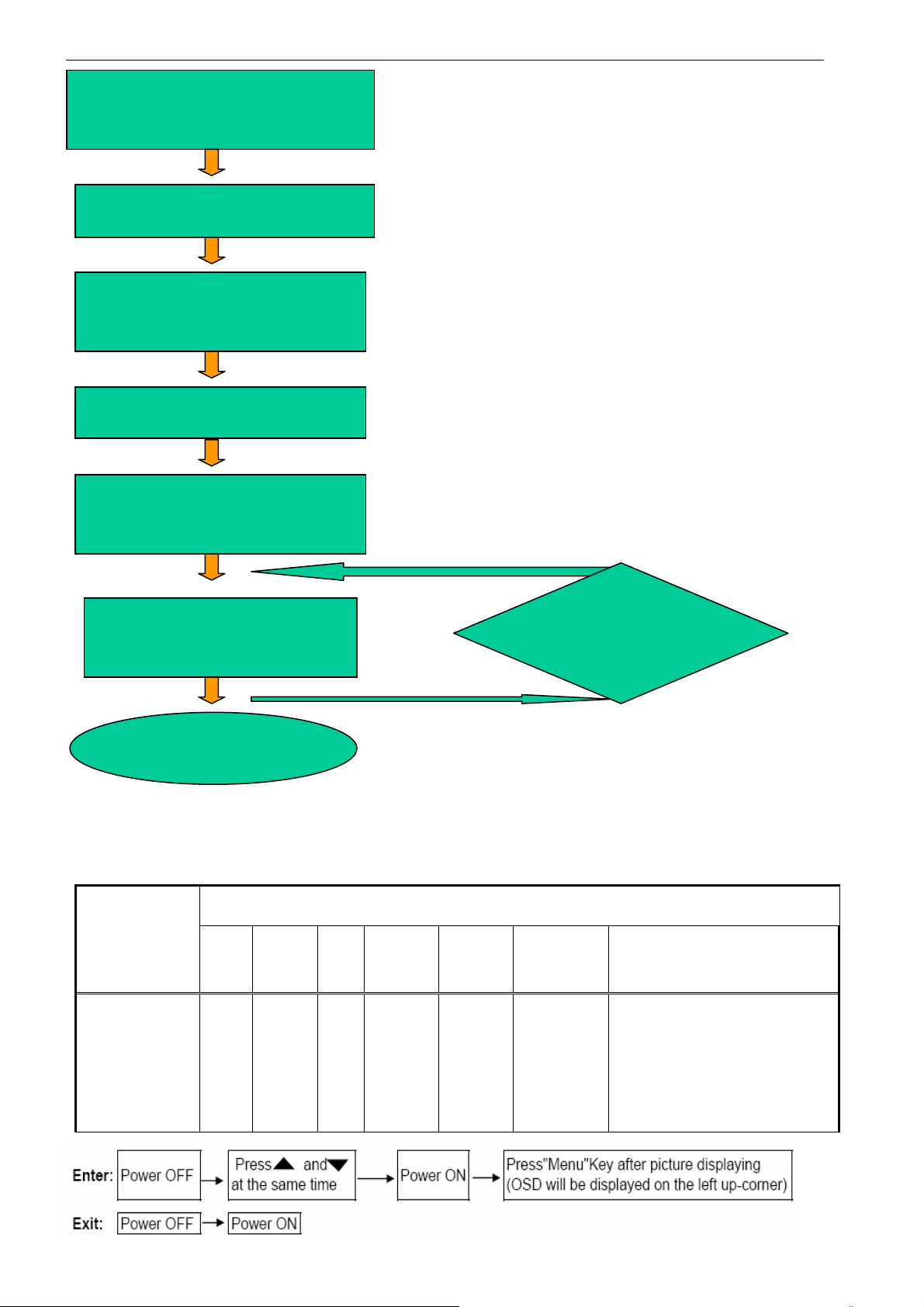
5.3 OSD Structure
The On-Screen Display (OSD) shall be an easy to use icon based menu through keypad OSD
buttons or remote control unit. The unit shall leave the factory with all OSD controls set to
their default values.
First Second Third Control Range Default Value
Brightness
ACER e COLOR
Management
User
Empowering
Technology
User mode
Text mode 50
Contrast
Standard mode 50
Graphics mode 60
Movie mode 56
Brightness
10
User mode
50
77
Page 12
ACM
Text mode 44
Standard mode 77
Graphics mode 97
Movie mode 77
OFF
Image
Position
Color
Language
OSD
Input (Dual)
Input (Analg
only)
Focus
Clock
Horizontal
Vertical
Warm (6500K)
Cool (9300K)
User
NO-EMEA EMEA
English English
Deutsch Deutsch
Español Español
简体中文
繁體中文
Français Français
Italiano Italiano
日本語
Hor. Position
Ver. Position
OSD Timeout
Analog
Digital
DDCCI ON/OFF
DDCCI ON/OFF
Hollands
Русский
Suomalain
---
---
---
---
--- ---
--- ---
Red
Green
Blue
--- ---
--- ---
--- ---
--- ---
--- ---
--- ---
--- ---
--- ---
---
---
---
--- --- ---
--- --- -- ON
ON
0 ~ 100
0 ~ 100
0 ~ 100
0 ~ 100
0 ~ 100
0 ~ 100
0 ~ 100
Depend on each timing
50 ○1
50
Depend on each timing
80
80
80
English
0 ~ 100 50
0 ~ 100 50
10~ 120 20
Info
Reset
Exit
Resolution
H. Freq
V. Freq
S/N
--- --- --- ---
--- --- --- ---
--- --- ---
--- --- ---
--- --- -- ETL000….0000(22)
Notes; ○1 Clock default 50 is for Visa timing. Others depend on timing.
6.0 SOP of firmware upgrade -----Manufacturer of Scaler is RealTek
6.1 Operational condition
Equipment: PC, ISP card, signal cable and power cable.
ESD requirements: antistatic wrists, antistatic gloves (fingers), and connecting
cable
11
Page 13
Name of ISP program: RTDTool_4.6.exe
Manufacture of FW IC:RTD 2525L
6.2 Operational steps:
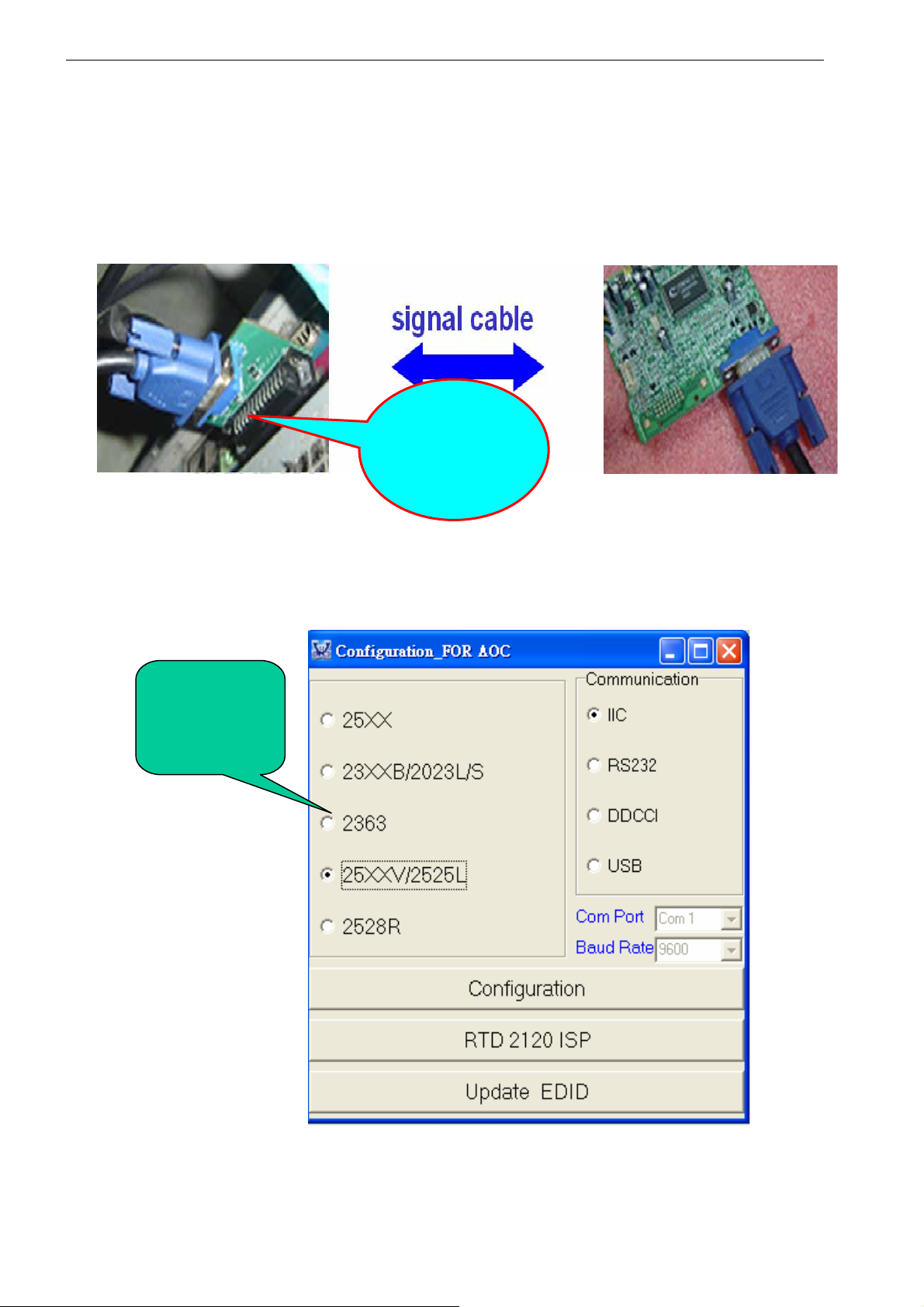
1. Connection: connect PC to PCBA with signal cable, and then keep AC and DC in open
state.
2. Adjust ISP programming
Firstly, double click RTDTool_4.6.exe and open ISP program, then select
“25XXV/2525L”, and RTD 2120 ISP button
One port of ISP
program card is
connected to PC
print port.
Click ISP
button
12
Page 14
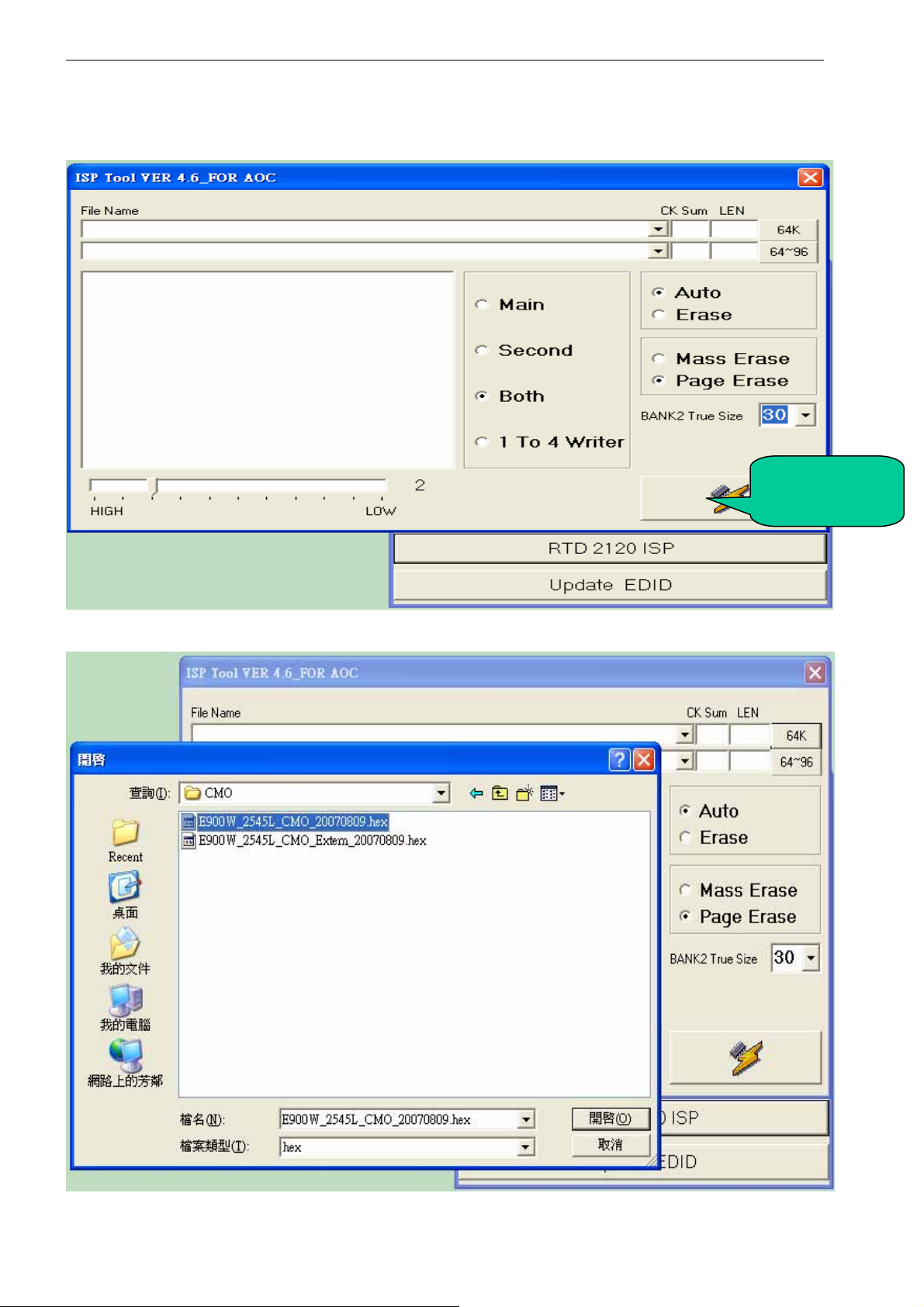
Secondly﹐ select Bank2 size which is 30.
Select Bank2
size: 30
Thirdly, click “64K”button and download FW file as below Figure 3.
13
Page 15
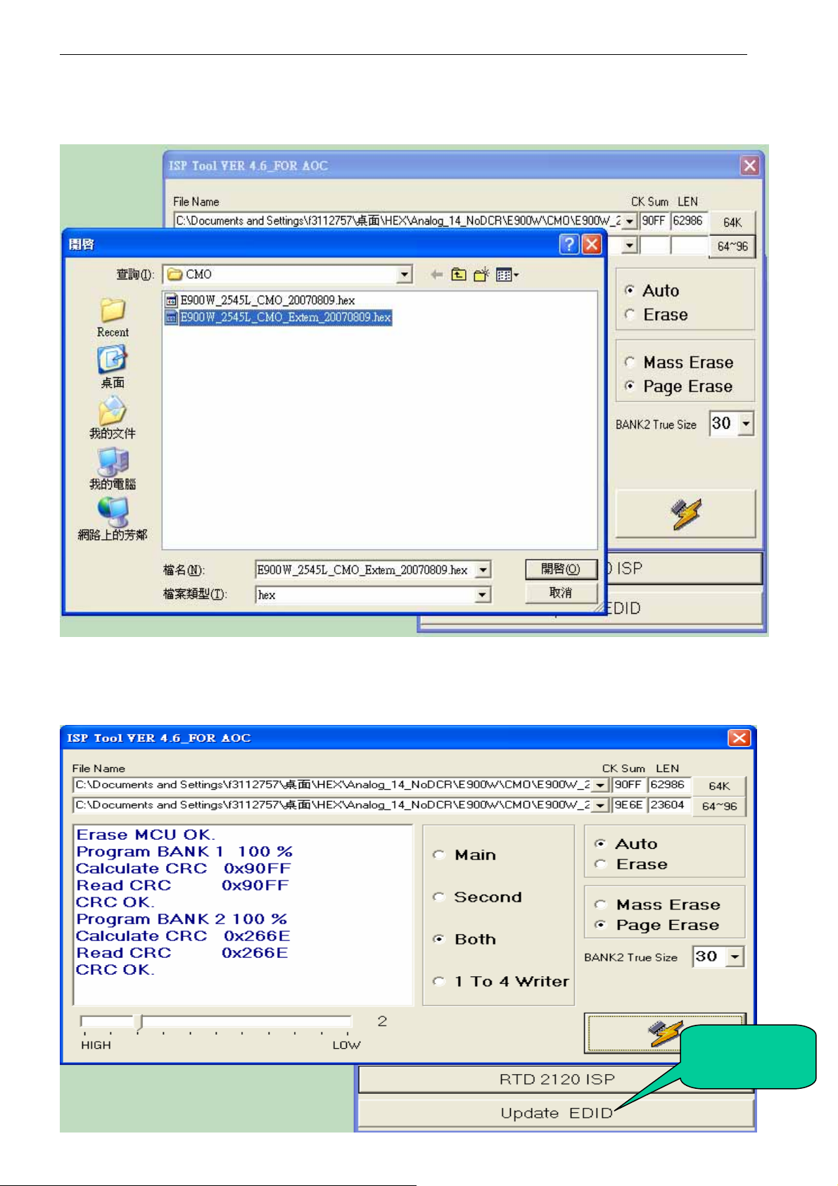
Fourthly, click “64~96”button, and download extern FW file as below Figure 4 .
Fifthly, click “program”button as below,then you will see ISP will going on. There will be
prompting if programming is OK.
14
Program
button
Page 16
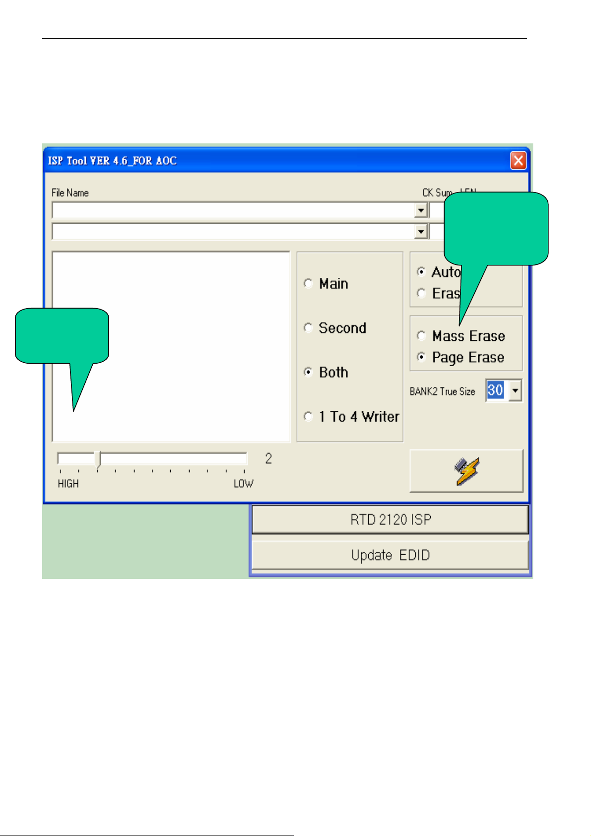
Note: Please see the configure as below Figure 6.
Configure
Inform
Programmi
ng speed
15
Page 17
g
prog
After connecting, AC
ON, DC ON
OK
Open ISP program
OK
Choose
manufacturer and
OK
LOAD FW files
OK
Click program
button
OK
◆Flowin
chart
Beginning
programming
OK
Turn off power if
ramming is OK
6.3 Factory Mode
FUNCTION
AUTO
FACTORY MODE
●
e Color
Choose Config
and adjust
programming
NG
HOT KEY OPERATION
◄ ► MENU POWER
●
ON
Press [e Color ] & [MENU] at the
same time, and then press
[POWER] for DC power on. OSD
menu will be shown with “F” on the
left top. Select “F” for entering
factory mode.
16
Page 18
02. Flat Panel Specification
17
Page 19

HannStar Display Corp.
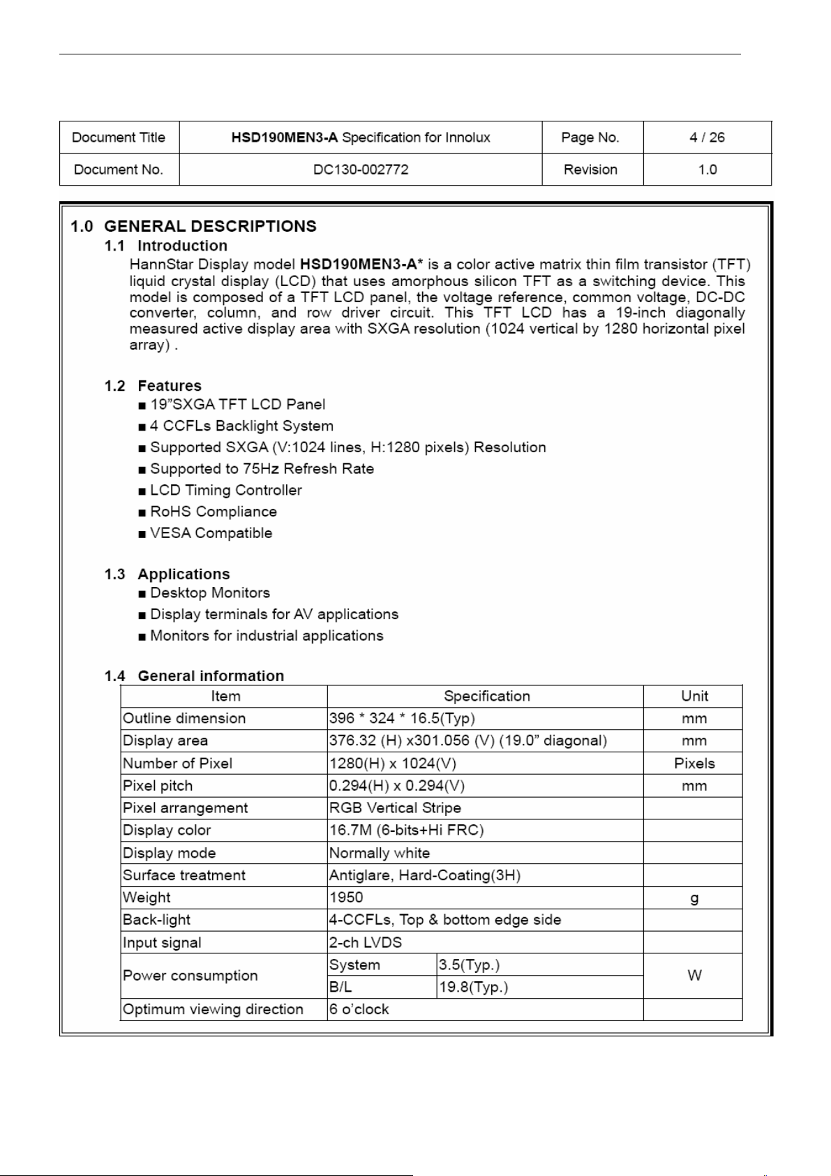
Document Title HSD190MEN3-A Specification for Innolux Page No. 4 / 26
Document No. DC130-002772 Revision 1.0
1.0 GENERAL DESCRIPTIONS
1.1 Introduction
HannStar Display model HSD190MEN3-A* is a color active matrix thin film transistor (TFT)
liquid crystal display (LCD) that uses amorphous silicon TFT as a switching device. This
model is composed of a TFT LCD panel, the voltage reference, common voltage, DC-DC
converter, column, and row driver circuit. This TFT LCD has a 19-inch diagonally
measured active display area with SXGA resolution (1024 vertical by 1280 horizontal pixel
array) .
1.2 Features
■ 19”SXGA TFT LCD Panel
■ 4 CCFLs Backlight System
■ Supported SXGA (V:1024 lines, H:1280 pixels) Resolution
■ Supported to 75Hz Refresh Rate
■ LCD T iming Controller
■ RoHS Compliance
■ VESA Compatible
1.3 Applications
■ Desktop Monitors
■ Display terminals for AV applications
■ Monitors for industrial applications
1.4 General information
Item Specification Unit
Outline dimension 396 * 324 * 16.5(Typ) mm
Display area 376.32 (H) x301.056 (V) (19.0” diagonal) mm
Number of Pixel 1280(H) x 1024(V) Pixels
Pixel pitch 0.294(H) x 0.294(V) mm
Pixel arrangement RGB Vertical Stripe
Display color 16.7M (6-bits+Hi FRC)
Display mode Normally white
Surface treatment Antiglare, Hard-Coating(3H)
Weight 1950 g
Back-light 4-CCFLs, Top & bottom edge side
Input signal 2-ch LVDS
Power consumption
Optimum viewing direction 6 o’clock
System 3.5(Typ.)
B/L 19.8(Typ.)
W
The information contained in this document is the exclusive property of HannStar Display Corporation. It shall not
be disclosed, distributed or reproduced in whole or in part without written permission of HannStar Display
Corporation.
Page 20

HannStar Display Corp.
Document Title HSD190MEN3-A Specification for Innolux Page No. 5 / 26
Document No. DC130-002772 Revision 1.0
1.5 Mechanical Information
Item Min. Typ. Max. Unit
Horizontal(H) 395.5 396.0 396.5 mm
Module Size
Vertical(V) 323.5 324.0 324.5 mm
Depth(D) 16.5 mm
Weight (without inverter) -- 1950 -- g
Torque of customer screw hole -- -- 3.0 Kgf*Cm
2.0 ABSOLUTE MAXIMUM RATINGS
2.1 Absolute Rating of Environment
Item Symbol Min. Max. Unit Note
Storage temperature T
Operating temperature T
Vibration (non-operating) V
Shock (non-operating) S
Storage humidity H
Operating humidity HOP 10 80 %RH (4)
Low pressure (operating) P
Low pressure (non-operating) P
Note (1)Storage /Operating temperature
Humidity (%)
Storage Range
-20-40
The information contained in this document is the exclusive property of HannStar Display Corporation. It shall not
be disclosed, distributed or reproduced in whole or in part without written permission of HannStar Display
Corporation.
-20 60 oC
STG
0 50 oC (1)
OPR
-- 1.5 G (2)
NOP
-- 70 G (3)
NOP
10 90 %RH (3)
STG
697 -- HPa (5)
LOP
116 -- HPa (6)
LNOP
100
90
80
60
40
20
10
0
Operating Range
0
Temperature (
20 40 60
o
C)
50
65
Page 21

HannStar Display Corp.
Document Title HSD190MEN3-A Specification for Innolux Page No. 6 / 26
Document No. DC130-002772 Revision 1.0
(2) 5-500-5Hz sine wave, X,Y,Z each directions, 30 min/cycle.
(3) 11ms, ±X, ±Y, ±Z direction, one time each. For this shock test,
It is necessary to fill the silicon rubber between the shock jig as buffer.
(4) Max wet bulb temp. =39
(5) 2 hrs. (10000 feet)
(6) 24hrs. (50000 feet)
2.2 Electrical Absolute Rating:
2.2.1 TFT LCD Module:
o
C
Item Symbol Min. Max. Unit. Note
Power supply Voltage VDD -0.3 5.5 V(DC) (1)(2)
2.2.2 Back Light Unit:
Item Symbol Min. Max. Unit Note
Lamp current
Lamp frequency
IL
fL
3.0 8.0 mA (1)(2)(3)
40 80 KHz (1)(2)(3)
Note: (1) Permanent damage may occur to the LCD module if beyond this specification.
Functional operation should be restricted to the conditions described under
Normal Operating Conditions.
(2) To exceed 7.5mA, life time accelerate drop down and if to exceed 8.0 mA has
safety problem. If current lower than 3.0 mA, CCFL would be unstable or
damaged.
(3) Within Ta=25±2°C
The information contained in this document is the exclusive property of HannStar Display Corporation. It shall not
be disclosed, distributed or reproduced in whole or in part without written permission of HannStar Display
Corporation.
Page 22

HannStar Display Corp.
Document Title HSD190MEN3-A Specification for Innolux Page No. 7 / 26
Document No. DC130-002772 Revision 1.0
3.0 OPTICAL CHARACTERISTICS
3.1 Optical specification
Item Symbol Condition Min. Typ. Max. Unit Note
Contrast CR 700 1000 -- (1)(2)
Response time
Rising --
Falling
TR +TF
--
5.0 10 msec (1)(3)
White luminance
(center of screen)
Red
Gree
Color
n
chromaticity
(CIE1931)
Blue
White
Hor.
Viewing angle
Ver.
Hor.
Viewing angle
Ver.
Brightness uniformity B
250 300 -- cd/m2
Y
L
Rx
Ry
Gx
Gy
Bx
By
Wx
Wy
o
Θ=0
o
φ=0
Normal
viewing
angle
-0.03
0.641
0.337
0.304
0.620
0.141
0.073
0.313
0.329
+0.03
ΘL 75 85 --
75
Θ
R
CR>10
ΘH 75
Θ
L
75
85
80
80
--
--
--
ΘL 75 85 --
75 85 --
Θ
R
CR>5
ΘH 75 85 --
Θ
UNI
L
o
Θ=0
φ=0
o
75 85 -75 -- -- % (6)
(1)(4)
(IL=7.5mA)
(1)(4)
3.2 Measuring Condition
■ Measuring surrounding : dark room
■ Lamp current I
■ V
=5.0V, fV=60Hz, f
DD1
■ Surrounding temperature : 25±2
■ 30min. Warm-up time.
The information contained in this document is the exclusive property of HannStar Display Corporation. It shall not
be disclosed, distributed or reproduced in whole or in part without written permission of HannStar Display
Corporation.
: (7.5)±0.1mA, lamp freq. FL=48 KHz, Inverter: TBD
BL
=54MHz
DCLK
o
C
Page 23

HannStar Display Corp.
Document Title HSD190MEN3-A Specification for Innolux Page No. 8 / 26
Document No. DC130-002772 Revision 1.0
3.3 Measuring Equipment
■ FPM520 of Westar Display technologies, INC., which utilized SR-3 for Chromaticity and
BM-5A for other optical characteristics.
■ Measuring spot size : 20~21mm
Note (1) Definition of Viewing Angle:
ΦH
12’ o’clock
H
=90
o
Φ
ΘL
Θ
R
ΘL=90o
ΘR=90o
ΦL
Note (2) Definition of Contrast Ratio(CR) :
measured at the center point of panel
Luminance with all pixels white (L255)
CR =
Luminance with all pixels black (L0)
6’ o’clock
=90
L
o
Φ
The information contained in this document is the exclusive property of HannStar Display Corporation. It shall not
be disclosed, distributed or reproduced in whole or in part without written permission of HannStar Display
Corporation.
Page 24

HannStar Display Corp.
Document Title HSD190MEN3-A Specification for Innolux Page No. 9 / 26
Document No. DC130-002772 Revision 1.0
Note (3) Definition of Response Time: Sum of T
and TF
R
white(TFT OFF) black (TFT ON) white(TFT OFF)
100%
90%
T
R
T
F
Optical
response
10%
0%
time
Note (4) Optical characteristic measurement setup
LCD Panel
Field = 1
o
120cm
Photo-detector (BM-5A)
The information contained in this document is the exclusive property of HannStar Display Corporation. It shall not
be disclosed, distributed or reproduced in whole or in part without written permission of HannStar Display
Corporation.
Page 25

HannStar Display Corp.
Document Title HSD190MEN3-A Specification for Innolux Page No. 10 / 26
Document No. DC130-002772 Revision 1.0
Note (5) Definition of Center Luminance of White (center)
Center Luminance= Y1
1/10V
1/10 H
1/2H
1/10H
Y1
1/2V
1/10V
Note (6) Definition of brightness uniformity
Luminance uniformity = x 100%
(Min Luminance of 9 points)
(Max Luminance of 9 points)
The information contained in this document is the exclusive property of HannStar Display Corporation. It shall not
be disclosed, distributed or reproduced in whole or in part without written permission of HannStar Display
Corporation.
Page 26

HannStar Display Corp.
Document Title HSD190MEN3-A Specification for Innolux Page No. 11 / 26
Document No. DC130-002772 Revision 1.0
4.0 BLOCK DIAGRAM
4.1 LCD Module Block Diagram:
Connector CN1
Converter
TCON with
LVDS receiver
DC/DC
Y-driver IC
X-driver IC
Liquid Crystal Panel
1280×1024 pixels
Gamma
Reference
Voltage
Generator
The information contained in this document is the exclusive property of HannStar Display Corporation. It shall not
be disclosed, distributed or reproduced in whole or in part without written permission of HannStar Display
Corporation.
Page 27

HannStar Display Corp.
Document Title HSD190MEN3-A Specification for Innolux Page No. 12 / 26
Document No. DC130-002772 Revision 1.0
4.2 Back Light Unit
1 Hot 1
2 Cold 1
1 Hot 2
2 Cold 2
Back light lamp
CN2, 3, 4, 5.
4.3 Pixel Format
1 Hot 1
2 Cold 1
1 Hot 2
2 Cold 2
1,1
1,2
1,3
(odd)
2,1
(odd)
(even)
(odd)
1,4
(even)
LCD Display Area
1280
1,
1024
,1
1
Pixel
R
G
R
R
B
1024
1280
1024 Lines
1280 Pixels
The information contained in this document is the exclusive property of HannStar Display Corporation. It shall not
be disclosed, distributed or reproduced in whole or in part without written permission of HannStar Display
Corporation.
Page 28

HannStar Display Corp.
Document Title HSD190MEN3-A Specification for Innolux Page No. 13 / 26
Document No. DC130-002772 Revision 1.0
4.4 Relationship Between Displayed Color and Input
MSB LSB MSB LSB MSB LSB Gray scale
Display
Black L L L L L L L L L L L L L L L L L L L L L L L L -
Blue L L L L L L L L L L L L L L L L H H H H H H H H -
Green L L L L L L L L H H H H H H H H L L L L L L L L Basic
color
Gray scale
of Red
Gray scale
of Green
Gray scale
of Blue
Gray scale
of White &
Black
Light Blue L L L L L L L L H H H H H H H H H H H H H H H H -
Red H H H H H H H H L L L L L L L L L L L L L L L L Purple H H H H H H H H L L L L L L L L H H H H H H H H Yellow H H H H H H H H H H H H H H H H L L L L L L L L -
White H H H H H H H H H H H H H H H H H H H H H H H H Black L L L L L L L L L L L L L L L L L L L L L L L L L0
Dark L L L L L L H L L L L L L L L L L L L L L L L L L2
Light H H H H H H L H L L L L L L L L L L L L L L L L L253
Red H H H H H H H H L L L L L L L L L L L L L L L L Red L255
Black L L L L L L L L L L L L L L L L L L L L L L L L L0
Dark L L L L L L L L L L L L L L H L L L L L L L L L L2
Light L L L L L L L L H H H H H H L H L L L L L L L L L253
Green L L L L L L L L H H H H H H H H L L L L L L L L Green L255
Black L L L L L L L L L L L L L L L L L L L L L L L L L0
Dark L L L L L L L L L L L L L L L L L L L L L L H L L2
Light L L L L L L L L L L L L L L L L H H H H H H L H L253
Blue L L L L L L L L L L L L L L L L H H H H H H H H Blue L255
Black L L L L L L L L L L L L L L L L L L L L L L L L L0
Dark L L L L L L H L L L L L L L H L L L L L L L H L L2
Light H H H H H H L H H H H H H H L H H H H H H H L H L253
White H H H H H H H H H H H H H H H H H H H H H H H H White L255
R7 R6 R5 R4 R3 R2 R1 R0 G7 G6 G5 G4 G3 G2 G1 G0 B7 B6 B5 B4 B3 B2 B1 B0
L L L L L L L H L L L L L L L L L L L L L L L L L1
↑ ︰ ︰ ︰ L3…L251
↓
H H H H H H L L L L L L L L L L L L L L L L L L L252
H H H H H H H L L L L L L L L L L L L L L L L L L254
L L L L L L L L L L L L L L L H L L L L L L L L L1
↑ ︰ ︰ ︰ L3…L251
↓
↑ ︰ ︰ ︰ L3…L251
↓
↑ ︰ ︰ ︰ L3…L251
↓
L L L L L L L L H H H H H H L L L L L L L L L L L252
L L L L L L L L H H H H H H H L L L L L L L L L L254
L L L L L L L L L L L L L L L L L L L L L L L H L1
L L L L L L L L L L L L L L L L H H H H H H L L L252
L L L L L L L L L L L L L L L L H H H H H H H L L254
L L L L L L L H L L L L L L L H L L L L L L L H L1
H H H H H H L L H H H H H H L L H H H H H H L L L252
H H H H H H H L H H H H H H H L H H H H H H H L L254
Level
The information contained in this document is the exclusive property of HannStar Display Corporation. It shall not
be disclosed, distributed or reproduced in whole or in part without written permission of HannStar Display
Corporation.
Page 29

HannStar Display Corp.
Document Title HSD190MEN3-A Specification for Innolux Page No. 14 / 26
Document No. DC130-002772 Revision 1.0
5.0 I/O CONNECTION PIN ASSIGNMENT
5.1 Interface Connector (30-pins, HRS MDF76URW-30S-1H or equivalent)
Pin No. Signal Description
1 RinO0- Receiver Signal (-)
2 RinO0+ Receiver Signal (+)
3 RinO1- Receiver Signal (-)
4 RinO1+ Receiver Signal (+)
5 RinO2- Receiver Signal (-)
6 RinO2+ Receiver Signal (+)
7 VSS Ground
8 RinOC- Clock Signal (-)
9 RinOC+ Clock Signal (+)
10 RinO3- Receiver Signal (-)
11 RinO3+ Receiver Signal (+)
12 RinE0- Receiver Signal (-)
13 RinE0+ Receiver Signal (+)
14 VSS Ground
15 RinE1- Receiver Signal (-)
16 RinE1+ Receiver Signal (+)
17 VSS Ground
18 RinE2- Receiver Signal (-)
19 RinE2+ Receiver Signal (+)
20 RinEC- Clock Signal (-)
21 RinEC+ Clock Signal (+)
22 RinE3- Receiver Signal (-)
23 RinE3+ Receiver Signal (+)
24 VSS Ground
25 VSS Ground
26 NC NC
27 VSS Ground
28 VDD+5V Power Supply, 5V (Typical)
29 VDD+5V Power Supply, 5V (Typical)
30 VDD+5V Power Supply, 5V (Typical)
5.2 Back Light Unit (CCFL) Connectors:
CN2, 3, 4, 5: CCFL Power Source (Yeonho 35001H5-02 or equivalent)
Pin No. Symbol Color Function
1 Hot1 Pink CCFL power supply (High voltage)
2 Cold1 White Ground
The information contained in this document is the exclusive property of HannStar Display Corporation. It shall not
be disclosed, distributed or reproduced in whole or in part without written permission of HannStar Display
Corporation.
Page 30

HannStar Display Corp.
Document Title HSD190MEN3-A Specification for Innolux Page No. 15 / 26
Document No. DC130-002772 Revision 1.0
6.0 ELECTRICAL CHARACTERISTICS
6.1 TFT LCD Module:
Item Symbol Min. Typ. Max. Unit Note
Voltage of power supply VDD 4.5 5.0 5.5 V
White I
Current of power
supply
V-Color I
Mosaic I
Vsync frequency fV 56 60 76 Hz (2)
Hsync frequency fH 64 64 80 KHz
Frequency f
Input rush current I
Note (1)
(a)White:
405 480 555 mA (1)
DD0
DD1
DD2
DCLK
RUSH
500 600 700
810 1010 1210
mA (1)
mA (1)
50 54 67.5 MHz
-- -- 3.0 A (3)
(b).V-Color :
Yellow
White
Purple
Red
Cyan
Green
Blue
Black
The information contained in this document is the exclusive property of HannStar Display Corporation. It shall not
be disclosed, distributed or reproduced in whole or in part without written permission of HannStar Display
Corporation.
Page 31

HannStar Display Corp.
Document Title HSD190MEN3-A Specification for Innolux Page No. 16 / 26
Document No. DC130-002772 Revision 1.0
(c)Mosaic : 2 Dot checker image
L0
Grey scale:L0~L255
L0: Luminance with all pixels black.
L255: Luminance with all pixels white.
Note (2) When fv is too low, a flicker may be occurred on the display.
Note (3) Input Rush Current condition
L31
0.9VDD
5 V
GND
0.1VDD
500us~10ms
The information contained in this document is the exclusive property of HannStar Display Corporation. It shall not
be disclosed, distributed or reproduced in whole or in part without written permission of HannStar Display
Corporation.
Page 32

HannStar Display Corp.
Document Title HSD190MEN3-A Specification for Innolux Page No. 17 / 26
Document No. DC130-002772 Revision 1.0
6.2 Back-Light Unit
The back-light system is an edge-lighting type with 4 CCFL
(Cold Cathode Fluorescent Lamp).
The characteristics of the lamp are shown in the following tables.
Item Symbol Min. Typ. Max. Unit Note
Lamp current IL 3.0 7.5 8.0 mA(rms) (1)
Lamp voltage VL 594 660 726 V(rms) IL=7.5mA
Frequency fL 40 50 80 KHz (2)
Operating Lifetime Hr 40,000 -- -- Hour 7.5mA(3)
Startup voltage Vs
1400 at 25oC
1650
-- -- V(rms)
at 0
o
C
LCD MODULE
1
2
1
2
1
2
1
2
1
2
1
2
1
2
1
2
A
A
A
A
INVERTER
(TBD332NR)
Note (1)
Lamp current is measured with current meter for high frequency as shown below. Specified
values are for a single lamp. To exceed 7.5 mA, life time accelerate drop down and if to
exceed 9.0 mA has safety problem. If current lower than 3.5 mA, CCFL would be unstable or
damaged.
Note (2)
Lamp frequency may produce interference with horizontal synchronous frequency and this
may cause ripple noise on the display. Therefore lamp frequency shall be kept away from the
horizontal synchronous frequency and its harmonics as far as possible in order to avoid
interference.
Note (3)
Lamp life time (Hr) can be defined as the time in which it continues to operate under the
condition : Ta=25±3
o
C, Typical IL value indicated in the above table and fL=48 kHz until the
brightness becomes less than 50%
The information contained in this document is the exclusive property of HannStar Display Corporation. It shall not
be disclosed, distributed or reproduced in whole or in part without written permission of HannStar Display
Corporation.
Page 33

HannStar Display Corp.
Document Title HSD190MEN3-A Specification for Innolux Page No. 18 / 26
Document No. DC130-002772 Revision 1.0
Note (4)
CCFL inverter should be able to provide a voltage over specified value (Vs) in the above
table. Lamp units need at least Vs value shown above to ignition.
Note (5)
The voltage over specified value (Vs) should be applied to the lamp more than 1 second
after startup. Otherwise, the lamp may not be turned on. The used lamp current is the lamp
typical current.
Note (6)
The output voltage waveform and current waveform of the inverter must be symmetrical
(Unsymmetrical ratio is less than 10%). Please do not use the inverter which has
unsymmetrical voltage and current waveform, and spike waveform. The inverter design
which can provide the best optical performance, power efficiency, and lamp life should under
the following conditions.
a. The asymmetry rate of the inverter waveform should be less than 10%.
b. The distortion tae of the waveform should be within √2±10%.
c. The inverter output waveform should be better similar to the ideal sine wave.
Ip
I-p
Asymmetry rate = |I
Distortion rate = I
p-I-p| / Irms x 100%
p (or I-p) / Irms
The information contained in this document is the exclusive property of HannStar Display Corporation. It shall not
be disclosed, distributed or reproduced in whole or in part without written permission of HannStar Display
Corporation.
Page 34

HannStar Display Corp.
Document Title HSD190MEN3-A Specification for Innolux Page No. 19 / 26
Document No. DC130-002772 Revision 1.0
6.3 Interface Timing ( DE mode)
Item Symbol Min. Typ. Max. Unit
Frame Rate -- 56 60 76 Hz
Frame Period t1 1028 1066 1150 line
Vertical Display Time t2 1024 1024 1024 line
Vertical Blanking Time t3 4 42 126 line
1 Line Scanning Time t4 780 844 875 clock
Horizontal Display Time t5 640 640 640 clock
Horizontal Blanking Time t6 140 204 235 clock
Clock Rate t7 50 54 67.5 MHz
Timing Diagram of Interface Signal (DE mode)
NCLK
DE
R,G,B[0:7]
NCLK
DE
R,G,B[0:7]
t4
X,1 X,2 X,3 X,4 X,Y
t7
t5 t6
123
4
7
5
6
91011
8
12
t1
t2 t3
X,
1022X,1023X,1024
t4
1271
1273
1275
1277
1269
1270
1272
1274
1276
1278
1279
1280
X,1 X,2
12345
6
The information contained in this document is the exclusive property of HannStar Display Corporation. It shall not
be disclosed, distributed or reproduced in whole or in part without written permission of HannStar Display
Corporation.
Page 35

HannStar Display Corp.
Document Title HSD190MEN3-A Specification for Innolux Page No. 20 / 26
Document No. DC130-002772 Revision 1.0
6.4 Power On / Off Sequence:
Power On
Power Off
Power Supply
0V
0V
0.1V
Signal
0.9VDD
DD
TP1
TP2
0.6V 0.6V
TP5
TP3
TP6
0.9V
DD
0.1V
DD
0.1VDD
TP4
Backlight
(Recommended)
50%
50%
Item Min. Typ. Max. Unit Remark
TP1 0.5 -- 10 msec
TP2 0 -- 50 msec
TP3 0 -- 50 msec
TP4 500 -- -- msec
TP5 200 -- -- msec
TP6 200 -- -- msec
Note:(1) The supply voltage of the external system for the module input should be the
same as the definition of VDD.
(2) Apply the lamp volatge within the LCD operation range. When the back-light
turns on before the LCD operation or the LCD truns off before the back-light turns
off, the display may momentarily become white.
(3) In case of VDD = off level, please keep the level of input signal on the low or
keep a high impedance.
(4) TP4 should be measured after the module has been fully discharged between
power off and on period.
(5) Interface signal shall not be kept at high impedance when the power is on.
The information contained in this document is the exclusive property of HannStar Display Corporation. It shall not
be disclosed, distributed or reproduced in whole or in part without written permission of HannStar Display
Corporation.
Page 36

HannStar Display Corp.
Document Title HSD190MEN3-A Specification for Innolux Page No. 21 / 26
Document No. DC130-002772 Revision 1.0
7.0 OUTLINE DIMENSION
7.1 Front View: Date: 2007.1.11
B
B
剖面視圖B-B
縮放: 3:1
Up
剖面視圖A-A
縮放: 3:1
A
A
Down
The information contained in this document is the exclusive property of HannStar Display Corporation. It shall not
be disclosed, distributed or reproduced in whole or in part without written permission of HannStar Display
Corporation.
Page 37

HannStar Display Corp.
Document Title HSD190MEN3-A Specification for Innolux Page No. 22 / 26
Document No. DC130-002772 Revision 1.0
7.2 Back View: Date: 2007.1.11
1.Backlight: 4 CCFL
2. I/F Connector Specification (CN1):
FI-XB30SSRL-HF16 or Equivalent
3. Lamp Connector (CN2~CN5) / Wire Specification:
Yeon-Ho 35001HS-02L or Equivalent / 2Pin x L170mm
4. User Mounting Torque Spec: 3 Kgf-cm Max.
5. Unspecificed Tolerance is ±0.5mm.
The information contained in this document is the exclusive property of HannStar Display Corporation. It shall not
be disclosed, distributed or reproduced in whole or in part without written permission of HannStar Display
Corporation.
Page 38

HannStar Display Corp.
Document Title HSD190MEN3-A Specification for Innolux Page No. 23 / 26
Document No. DC130-002772 Revision 1.0
8.0 LOT MARK
8.1 Lot Mark
1 2 3 4 5 6 7 8 9
10 11 12 13 14 15
code 1,2,3,4,5,6: HannStar internal fow control code.
code 7: production location.
code 8: production year.
code 9: production month.
code 10,11,12,13,14,15: serial number.
Note (1) Production Year
Year 1999 2000 2001 2002 2003 2004 2005 2006 2007 2008
Mark 9 0 1 2 3 4 5 6 7 8
Note (2) Production Month
Month Jan. Feb. Mar. Apr. May. Jun. Jul. Aug. Sep. Oct Nov. Dec.
Mark 1 2 3 4 5 6 7 8 9 A B C
8.2 Location of Lot Mark
(1) The label is attached to the backside of the LCD module.
(2) This is subject to change without prior notice.
HSD190MEN3
-A01
RoHS
Rev:
Lot mark
CN1
Up
Center of Active Area
CN5
CN3
CN4
CN2
Down
RISK OF ELECTRIC SHOCK DISCONNECT
THE ELECTRIC POWER BEFORE SERVICING
HIGH VOLTAGE CAUTION
COLD CATHODE FLUORESCENT LAMP IN LCD PANEL CONTAINS
A SMALL AMOUNT OF MERCURY. PLEASE FOLLOW LOCAL
ORDINANCES OR REGULATIONS FOR DISPOSAL.
The information contained in this document is the exclusive property of HannStar Display Corporation. It shall not
be disclosed, distributed or reproduced in whole or in part without written permission of HannStar Display
Corporation.
Page 39

HannStar Display Corp.
Document Title HSD190MEN3-A Specification for Innolux Page No. 24 / 26
Document No. DC130-002772 Revision 1.0
9.0 PACKAGE SPECIFICATION
9.1 Packing form
(1) package quantity in one carton: 8 pieces.
(2) carton size: 544±3 mm×302±3 mm×446
(3) for domestic transportation only.
9.2 Packing assembly draw ings
H
±3 mm.
M1904
8PCS
The information contained in this document is the exclusive property of HannStar Display Corporation. It shall not
be disclosed, distributed or reproduced in whole or in part without written permission of HannStar Display
Corporation.
Page 40

HannStar Display Corp.
Document Title HSD190MEN3-A Specification for Innolux Page No. 25 / 26
Document No. DC130-002772 Revision 1.0
10.0 GENERAL PRECAUTION
10.1 Use Restriction
This product is not authorized for use in life supporting systems, aircraft navigation
control systems, military systems and any other application where performance failure
could be life-threatening or otherwise catastrophic.
10.2 Disassembling or Modification
Do not disassemble or modify the module. It may damage sensitive parts inside LCD
module, and may cause scratches or dust on the display. HannStar does not warrant the
module, if customers disassemble or modify the module.
10.3 Breakage of LCD Panel
10.3.1 If LCD panel is broken and liquid crystal spills out, do not ingest or inhale liquid
crystal, and do not contact liquid crystal with skin.
10.3.2 If liquid crystal contacts mouth or eyes, rinse out with water immediately.
10.3.3 If liquid crystal contacts skin or cloths, wash it off immediately with alcohol and
rinse thoroughly with water.
10.3.4 Handle carefully with chips of glass that may cause injury, when the glass is
broken.
10.4 Electric Shock
10.4.1 Disconnect power supply before handling LCD module.
10.4.2 Do not pull or fold the CCFL cable.
10.4.3 Do not touch the parts inside LCD modules and the fluorescent lamp’s connector
or cables in order to prevent electric shock.
10.5 Absolute Maximum Ratings and Power Protection Circuit
10.5.1 Do not exceed the absolute maximum rating values, such as the supply voltage
variation, input voltage variation, variation in parts’ parameters, environmental
temperature, etc.otherwise LCD module may be damaged.
10.5.2 Please do not leave LCD module in the environment of high humidity and high
temperature for a long time.
10.5.3 It’s recommended employing protection circuit for power supply.
10.6 Operation
10.6.1 Do not touch, push or rub the polarizer with anything harder than HB pencil lead.
Use fingerstalls of soft gloves in order to keep clean display quality, when
persons handle the LCD module for incoming inspection or assembly.
10.6.2 When the surface is dusty, please wipe gently with absorbent cotton or other soft
material.
10.6.3 Wipe off saliva or water drops as soon as possible. If saliva or water drops
contact with polarizer for a long time, they may causes deformation or color
fading.
10.6.4 When cleaning the adhesives, please use absorbent cotton wetted with a little
petroleum benzene or other adequate solvent.
The information contained in this document is the exclusive property of HannStar Display Corporation. It shall not
be disclosed, distributed or reproduced in whole or in part without written permission of HannStar Display
Corporation.
Page 41

HannStar Display Corp.
Document Title HSD190MEN3-A Specification for Innolux Page No. 26 / 26
Document No. DC130-002772 Revision 1.0
10.7 Mechanism
Please mount LCD module by using mounting holes arranged in four corners tightly.
10.8 Static Electricity
10.8.1 Protection film must remove very slowly from the surface of LCD module to
prevent
from electrostatic occurrence.
10.8.2 Because LCD module uses CMOS-IC on circuit board and TFT-LCD panel, it is
very weak to electrostatic discharge. Please be careful with electrostatic
discharge.
10.8.3 Persons who handle the module should be grounded through adequate
methods.
10.9 Strong Light Exposure
The module shall not be exposed under strong light such as direct sunlight. Otherwise,
display characteristics may be changed.
10.10 Disposal
When disposing LCD module, obey the local environmental regulations.
The information contained in this document is the exclusive property of HannStar Display Corporation. It shall not
be disclosed, distributed or reproduced in whole or in part without written permission of HannStar Display
Corporation.
Page 42

03 Exploded Diagram
3.1 Screw List
3.1.1 LE19F7(B193 r & B193 h) Screw List
Item Part No. Description Qty
T(kg*cm)
SCREW,P,CROSS,W/WA
1 509146306200R
S,M3*6,Zn-Cc
BOLT,#4-40x11.8,Ni
2 509000000700R
ROHS
SCREW, P,CROSS
3 509146306102R
W/W-SPR,M3*6,Zn,
SCREW,B,CROSS,M4*12
4 509116612102R
,BLK-Zn,ROHS(NYLOK)#
4 6.5±0.5
4 3.75±0.25
3 6.5±0.5
4 12±0.5
Fixed
Remark
I/F Board to Chassis*1
Power Board to
Chassis*3
D-SUB CON*2
DVI CON*2
Power Board to
Chassis*3
HAS / Stand to
backcover
3.2.2 LE19F6(V193) Screw List
Item Part No. Description Qty
T(kg*cm)
SCREW,P,CROSS,W/WA
1 509146306200R
S,M3*6,Zn-Cc
BOLT,#4-40x11.8,Ni
2 509000000700R
ROHS
SCREW, P,CROSS
3 509146306102R
W/W-SPR,M3*6,Zn,
SCREW,B,CROSS,B.T-4*
4 509412610500R
10,BLK, ROHS
SCREW,F,CROSS,M4*8,
5 509216608110R
Zn,ROHS(NYLOK,35F)
4 6.5±0.5
4 3.75±0.25
3 6.5±0.5 Power Board to Chassis*3
3 10±0.5 Hinge to Stand
4 12±0.5 Hinge to backcover
Fixed
Remark
I/F Board to Chassis*1
Power Board to Chassis*3
D-SUB CON*2
DVI CON*2
19
Page 43

Page 44

Page 45

04 Troubleshooting
22
Page 46

23
Page 47

24
Page 48

2
V
R
S
H
05. Spare parts List
B Series Spare parts
INL
Item Description OEM Part No
1
2
3
4
5
6
7
8
9
PCBA,KEYPAD BOARD,LE9D0-612 ROHS 791401500000R
PCBA,P/I BOARD,W/O SPK,LE19F7-422ROHS 791401400411R
PCBA,I/F BOARD(EMEA,W/O SPK),LE19F7-42
PWRCORD 16A/250V BLK 6FT VDE/KTL H05V
CABLE,D-SUB 15P MALE 6FT BLACK/BLUE,
CABLE,DVI-D 18+1P MALE 6FT BLACK , ROH
HRN ASSY 2x4P to 8P 200mm UL1571#28,RO
HRN ASSY 2x4P 55mm UL1571#28,ROHS 430300801670R
HRN LVDS FFC 30P 205mm W/Core 430303001790R
791401300413R
453070801190R
453010100380R
453030300370R
430300801680R
P/N:8191F742A021
R
1
1
1
1
1
1
1
1
1
10
11
12
13
14
15
16
17
ASSY, BEZEL,B,SLIVER,LE19F7 714030019200R
ASSY, STAND, B173 H 714011203001R
ASSY,HINGE,B173H 714000005100R
ASSY,SWIVEL,LE17K0 714000005300R
ASSY,BACK COVER,B,BLACK,W/DVI,LE19F7 714050017401R
BASE, B173H 501240211300R
ASSY,CHASSIS,B,W/DVI,LE19F7 701000009801R
LCP 19" HSD190MEN3-A00(A)(HANNSTAR) 631102091100R
1
1
1
1
1
1
1
1
25
Page 49

0
05. Spare parts List (Continue)
V Series Spare parts
INL
Item Description OEM Part No
1
2
3
4
5
6
7
8
9
10
PCBA,I/F BOARD(EMEA,W/SPK)LE19F6-410,ROH 791401301403R
PCBA,P/I BOARD,W/SPK,LE19F6-410,ROHS 791401401401R
PCBA,KEYPAD BOARD,LE9D0-612 ROHS 791401500000R
PWRCORD 16A/250V BLK 6FT VDE/KTL H05VV-F 453070801190R
CABLE,D-SUB 15P MALE 6FT BLACK/BLUE, ROH 453010100380R
CABLE AUDIO 1P 6FT BLACK/GREEN CP03B06P
HRN ASSY 2x4P to 8P 200mm UL1571#28,ROHS 430300801680R
HRN ASSY 2x4P 75mm UL1571#28,ROHS 430300801800R
HRN LVDS FFC 30P 205mm W/Core 430303001790R
ASSY,BACK COVER,BLACK,W/AUDIO,LE19F6 714050017002R
453030300120R
P/N:8191F641A12
0R
1
1
1
1
1
1
1
1
1
1
11
12
13
14
15
16
17
18
ASSY, BEZEL,SLIVER,LE19F6 714030018100R
ASSY STAND PRAC LE19D1 714011202301R
ASSY,BASE,BLACK,LE19F6 714020014800R
COVER HINGE,BLACK RIGHT,LE19D1 501020220020R
COVER HINGE,BLACK LEFT,LE19D1 501020220021R
ASSY,CHASSIS,V,W/ AUDIO ,LE19F6 701000009402R
SPEAKER 2W 8? 260mm R/G/B W/CASE 618100200320R
LCP 19" HSD190MEN3-A00(A)(HANNSTAR) 631102091100R
1
1
1
1
1
1
1
1
26
Page 50

06 Schematics and Layouts
6.1 Inverter PWM circuit
27
Page 51

6.2 Switching Mode Power Supply circuit
28
Page 52

7.0 Assembly and Disassembly
Sequence Item Photo Procedures P/N Description
(1).Take panel out of box and place it on
the foam.
S1
Place panel
(2).Tear open the PE bag and put it in
the designated carton.
(3).Place panel on the foam like the
attached picture.
Remark:Do not touch the lamp cord and
place the surface of panel downsides on
the cushion.
631102091100
R
LCP 19"
HSD190MEN3A00(A)(HANNST
AR)
1.Check if the keypad and relevent wire
S2
S3
Insert
Keypay's wrie
Assemble
keypad
you choose are OK.
2.Insert the wire into the keypad like the
Picture
1.Check if there is any lacquer missed or
sctratch happened to the front bezel.
2.Insert the fixed keypad into the front
bezel as picture
430300801680
R
791401500000
R
HRN ASSY
2x4P to 8P
215mm
UL1571#28,RO
HS
PCBA,KEYPAD
BOARD,LE9D0612 ROHS
29
Page 53

p
Assembly and Disassembly (continue)
1.Reverse the panel by 180 degree,put
the surface of panel upsides and insert
front bezel in the panel.
2.Reverse the panel by 180 degree using
both hands,put the surface of panel
S4
S5
Assemble
front bezel
Insert FFC
wire into
mainboard
downsides and make sure FFC interface
is closer to operator.
3.Paste tinfoil on the position which refers
to attached picture,in order to cover the
gap in the panel completely.
Remark:Make sure the fixed job is
finished properly and lamp wire is closer
to right hand;Make the tinfoil smooth in
the corner of
(1).Insert FFC wire into its relevant
interface of mainboard properly like
attached picture1.
(2).Insert the short keypad into its
relevant interface like picture
(2).Put the fixed mainboard in the right
position.
anel.
714030018101
R
430303001500
R
ASSY,
BEZEL,BLACK,
LE19F6
HRN LVDS FFC
30P 182mm
ROHS
S6
Fix chassis
&poweboard
Place the chassis on the cushion after
check,like the attached Picture
30
701000009402
R
ASSY,CHASSIS
,V,W/ AUDIO
,LE19F6
Page 54

Assembly and Disassembly (continue)
S7
S8
Fix chassis
&poweboard
Connect
mainboard&po
werboard
Insert powerboard into the designated
location of chassis ,like the attached
Picture
Connent powerboard with the relevant
PIN in the mainboard like the attached
Picture
791401401401
R
791401301403
R
PCBA,P/I
BOARD,W/SPK,
LE19F6410,ROHS
PCBA,I/F
BOARD(EMEA,
W/SPK)LE19F6410,ROH
S9
Twist PCBA
screw(V193)
Handle electric opener and one pcs of
M3*6 screw
31
509146306200
R
SCREW,P,CRO
SS,W/WAS,M3*
6,Zn-Cc
Page 55

3
Assembly and Disassembly (continue)
MylarLocation
S10
S11
Twist PCBA
screw(B193)
Twist screw for
ground-wire
2
For B193 model , pls add 1pcs Mylar to
the chassis for to shelter from the hole in
the chassis before twist the second
screw, pls refer to the picture
505040209000
R
4
Paste FFC wire on the disignated
location like the attached Picture
Twist
S12
Hexagonal
screws
2
1
(1). Handle hexagonal screws and
electric opener
(2). Twist screw in the interface like the
attached Picture1.
(3). Place cushion on the designated
location after iron frame is taken away.
32
Page 56

Assembly and Disassembly (continue)
S13 Fix chassis
S14
Insert FFC
cable
Thread lamp wire into the relevant hole of
chassis like the attached Picture
1.Tear off the adhensive tape of FFC
wire;
2.Insert FFC wire into the interface of
panel
3.Put FFC wire in order and paste them
on the panel
4.Fix chassis on the back of panel
701000009402
R
ASSY,CHASSIS
,V,W/ AUDIO
,LE19F6
S15
Insert spearker
cable
Put 1pcs speaker cabel into the interface
of power board as picture
33
Page 57

Assembly and Disassembly (continue)
S16 Insert light wire
S17
Fix speaker
cabel
1 2
3
4
1)Insert 4pcs light wire into the relevant
position
2) put the balance light wire to the
position as picture
Fix the speaker into the two immobile
location on the chassis as picture
1)Insert keypad wire into the relevant PIN
in the keypad
2)Fix button on the relevant position of
(
assemble
3)Confirm if keypad is inserted properly
(
S18
Insert keypad
Cable
34
Page 58

4
Assembly and Disassembly (continue)
S19 Twist speaker
S20 Fix back cover
lock 2pcs screw into the chassis in
1
3
2
1
2
3
2
1
sequence as picture
Check if back cover is fixed properly
509146306200
R
501020220000
R
SCREW,P,CRO
SS,W/WAS,M3*
6,Zn-Cc
BACK
COVER,ALL,BL
ACK,INL V5
,LE19D1
2
S21
Fix
stand(B193)
3
Use 4pcs screw fix stand on the back of
assemble like attached Picture
35
509216608110
R
SCREW,F,CRO
SS,M4*8,Zn,
ROHS(NYLOK,3
5F)
Page 59

Assembly and Disassembly (continue)
SCREW,F,CRO
S22
Fix
stand(V193)
S23 Packing
2
3
1
4
Use 4pcs screw fix stand on the back of
assemble like attached Picture
(1)Release monitor to the packing line
(2)Put monitor into carton like the
attached picture
509216608110
R
SS,M4*8,Zn,
ROHS(NYLOK,3
5F)
36
 Loading...