

Page 1

Service guide files and updates are available
on the CSD web : for more information,
Please refer to http: csd.acer.com.tw
Acer AL1703
Service Guide
1
Page 2
2
Page 3
3
Page 4
4
Page 5
5
Page 6
6
Page 7

Table of Contents
Chapter 1 Monitor Features…………………………………….………. 8
1.1 Test Conditions……………………………………….………… 8
1.2 Features…………………….……………………………….… ... 8
1.3 LCD Panel Specification……………………………………... 9
Chapter 2 OPERATING INSTRUCTIONS… …………….………….……12
2.1 Function Name…………………………………………………12
2.2 OSD Menu Description… ..……………………………………14
2.3 OSD Control… ..…………………………………………………15
2.4 OSD Menu Screen……..……...……………………………….15
2.5 OSD Function Definition. …………………………………...…16
2.6 Plug and Play……….…………………………………………..17
2.7 Power Saver……………………………………………………..17
Chapter 3 Machine Disassembly and Assembly……..…….……18
3.1 Machine Disassembly…………………………………………18
3.2 Machine Assembly……………….…………………………... 21
Chapter 4 Troubleshooting… ………………….… .…….………….……25
4.1 Abnormal display Troubleshooting…………………………25
4.2 Abnormal (On/Off, LCD Display, K/B) Troubleshooting...27
4.3 Abnormal (BIOS, OSD, Other Display) Troubleshooting...28
4.4 Audio Abnormal………………………….…………………….29
Chapter 5 Connector Information… ………...……….………...……30
5.1 Function Block Diagram…………….…………………………30
5.2 Connector Location……..………….…………………………31
5.3 D-sub Mini 15Pin Connector…………………...… .…….……32
5.4 DC Connector…………...…………………….…….…….……32
5.5 Audio Connector………………………………...… .…….……32
5.6 Main Board Pin Assignment Introduction……….…….……32
Chapter 6 FRU(Field Replaceable Unit……...……….………………37
Chapter 7 Schematic Diagram …………….………………..…….……41
7
Page 8
Monitor Features
Chapter 1
1.1 Test Conditions
Item Condition
Temperature Normal room temperature (25±2℃)
Humidity 50±10%
AC input voltage 100V±2V, 120±2V, 60Hz / 240±2V, 50Hz
Brightness Maximum with OSD setting
Contrast Middle with OSD setting
Resolution setting 1280 x 1024 @60HZ
Color temperature With OSD setting
Measuring instrument Topcon luminance colorimeter BM-5A or equivalent
Others Before measuring, “Auto Adjust” & “Auto Balance” must be done in
advance
1.2 Features
l 17” SXGA TFT LCD Panel
l TN Mode Liquid Crystal
l D-SUB
l Audio Function (Optional)
l Support to 75Hz Refresh Rate
l Support VESA-DCC 2B plug & play function
l Support VESA-DPMS Power Management Function
l Super Wide Viewing Angle
l High Brightness & Contrast Ratio
l High Brightness & Contrast Angular Dependent
l Fast LC Response Time
l Light Weight
8
Page 9
1.3 LCD panel Specification
LC Response Time
12 o’clock direction
6 o’clock
Normal
Item Specification
Active Area 337.9 (H) x 270.34 (V) (17.0” diagonal)
Driver Element a-si TFT Active Matrix
Pixel Number 1280 x R.G.B. x 1024
Pixel Pitch 0.264 (H) x 0.264 (V)
Pixel Arrangement
Display Color 16.2M
LCD panel
Graphic
Performance
Tran missive Mode
Viewing Angle
(H/V)
Brightness 350
Contrast Ratio 350
(Tr+Tf)
Separate Sync. TTL Level
Horizontal Sync. Positive / Negative
Vertical Sync. Positive / Negative
Input Connector D-Sub mini 15 pins, DVI-D 24 pins (Optional)
Auto Adjust Clock, Phase, H Position & V Position
Screen Scaling VGA/SVGA/XGA/SXGA Full Screen Display
Power
Management
Color Adjustment User, 6500K, 7500K & 9300K
OSD Language English, French, German, Spanish, Italian, Japanese,
VESA DPMS, DVI DMPM, ENERGY STAR® Compliance
Traditional Chinese, Simplified Chinese, Russian, Korean
(1) Definition of Viewing Angle (θx, θy):
θx = θy = 0º
θX- = 90º
x-
θy- θy+
θx-
θy- = 90º
y-
θx+
RGB Vertical Stripe
Normally White
160 / 120
14 (Tr: 4 + Tf: 10)
y+
θy+ = 90º
x+
θX+ = 90º
9
Page 10
(2) Definition of Contrast Ratio (CR):
: test point
1 2 3 0
4
100%
Optical
The contrast ratio can be calculated by the following expression and figure
below.
Contrast Ratio (CR) = L255 / L0
L255: Luminance of gray level 255
L 0: Luminance of gray level 0
CR = CR (5)
CR (X) is corresponding to the Contrast Ratio of the point X at Figure in Note
(5).
Definition of luminance measured points and Brightness Uniformity:
0
256
512
768
1024
Vertical Line Number
Luminance of center point: L=L(5)
Brightness Uniformity Measurement points: Five specified points 1-5
Formula: Max imum [L (1), L (2), L (3), L (4), L (5)]/Minimum [L (1), L (2), L (3), L (4),
L (5)]
(3) Definition of Response Time (TR, TF):
Gray Level 255
90%
Response
10%
0%
T
R
Horizontal Line Number
320
640
5
Active area
960
Horizontal Line Number [pixel]
Gray Level 255
Gray Level 0
1280
X
X=1 to 5
T
F
Time
10
Page 11
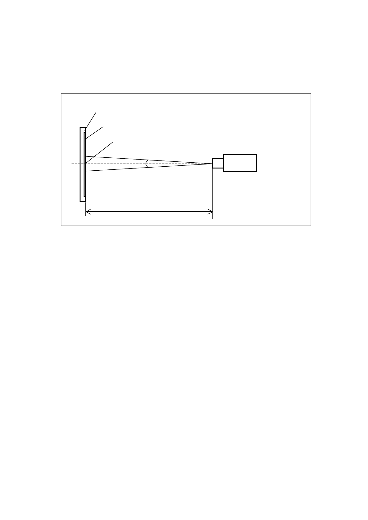
(4) Measurement Setup:
Light Shield Room
The LCD module should be stabilized at given temperature for 20 minutes
to avoid abrupt temperature change during measuring. In order to stabilize
the luminance, the measurement should be executed after lighting Backlight
for 20 minutes in a windless room.
LCD Module
LCD Panel
Center of the Screen
Field of View = 2º
500 mm
Photometer
(TOPCON BM-5A)
(Ambient Luminance < 2 lux)
11
Page 12
OPERATING INSTRUCTIONS
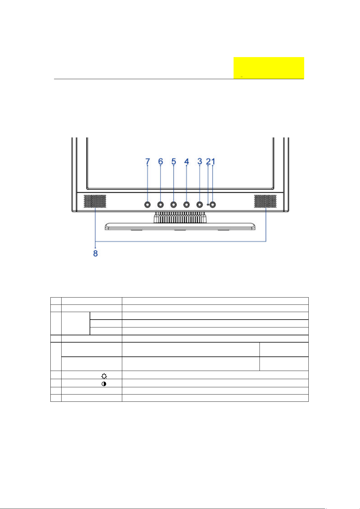
2.1 Function Name
2.1.1 Front
Chapter 2
No.
1
3
4
5
6
7
8
Key Descriptions
Power Switch Power on / Power off
LED
Indicator
INPUT/TURBO
Green/Blue Normal operation
Orange Power Management 2
Off Power off
AUTO/ EXIT Adjust Clock, Phase, H Position and V Position automatically / Exit
TURBO
+/ +/QUICK MENU Access (Brightness)
-/ -/QUICK MENU Access (Contrast)
MENU OSD control MENU button/Access Main/Sub -menu
Speaker 2.5W x 2
Turbo Brightness Switch
(Picture mode / Text mode / Economy mode)
D-Sub, DVI Input Source Selection/Turbo
Brightness Switch
A170E1- T01
A170E1- H01
12
Page 13
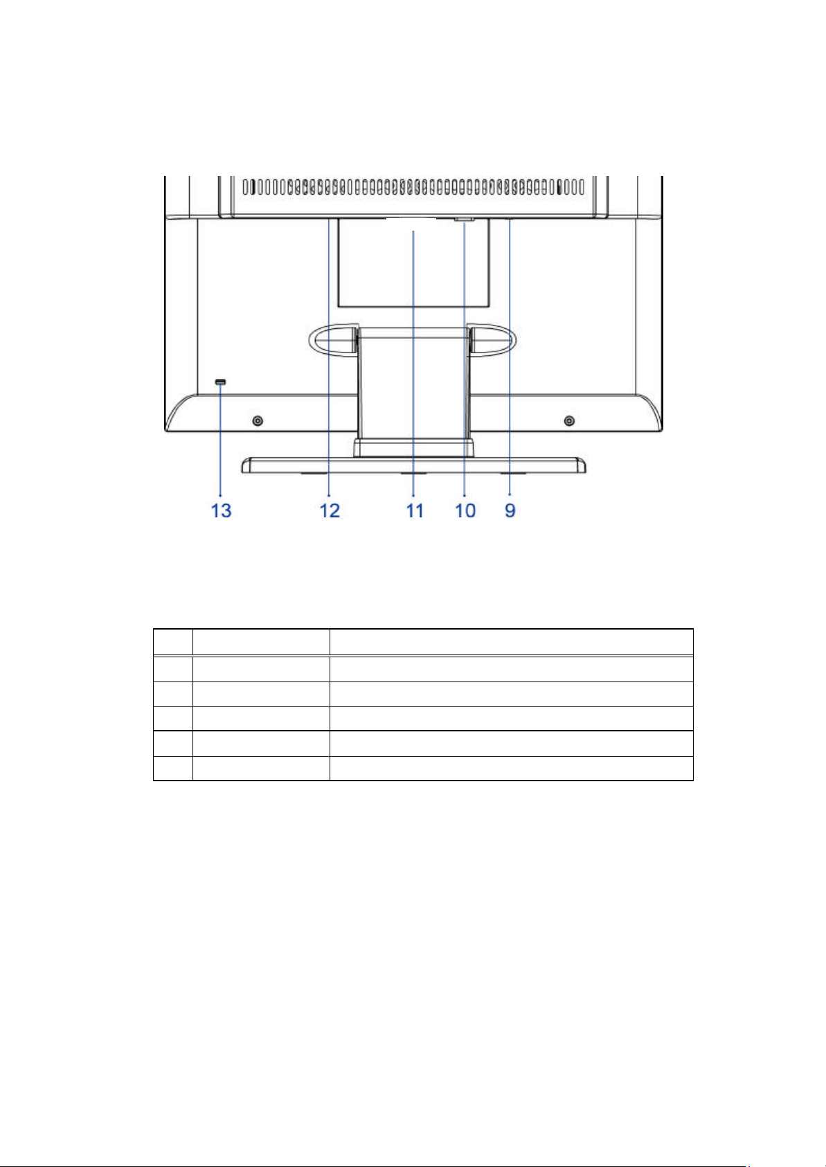
2.1.2 Back
No.
9. AUDIO-IN d=3.5mm stereo mini Jack
10.
11.
12.
13.
Name Descriptions
VGA-IN D-sub mini 15pin Connector
N/A N/A
DC-IN DC Power Jack, d=2.0mm.
Lock hole Kinglock
13
Page 14
Auto
/Exit
Input/
2.2 OSD Menu Description
1. Power : Press this key to control power ON/OFF of the Monitor.
Green: normal display.
Orange flicker: no signal input.
Orange: power off.
2. Auto/Exit : When the input signal source is PC, used to execute auto
adjustment
3. Input / Turbo : D-Sub, DVI input source selection
4. + / : Used to select the OSD function; when there is OSD menu,
used to increase function value.
Enter brightness control function directly when there is no
OSD menu.
5. —/ : Used to select the OSD function; when there is OSD menu,
used to decrease function value.
Enter contract control function directly when there is no OSD
menu.
6. Menu : Use to display OSD menu; when there is OSD menu, used to
execute OSD function or enter next layer of OSD menu; if
executing OSD function, exit OSD function and save the value
adjusted.
14
Menu
/
+ /
Power
Turbo
Page 15

Source Resolution & Frequency
Status
Image Adjustment
Volume Adjustment
2.3 OSD Control
u Press the “Menu” button to start the OSD feature.
u Click the “+” or “-“ button to select the function to be adjusted.
u Click the “Menu” button to access into the function to be adjusted.
u Click the “+” or “-“ button to change the current setting of the function.
u To exit the OSD menu or go back to the previous action by clicking
the “Auto/Exit” button. It will save the change automatically.
u To repeat above steps for changing the setting of other functions.
2.4 OSD Menu Screen
Color Temp. Selection
Language Selection
Settings
Input Source Selection (optional)
Audio Current Status
Color Temp. Status
Input Source Status (Optional)
u The OSD disappears several seconds after you stop pressing the
buttons while performing an adjustment.
u Any changes are automatically saved in the memory when the OSD
disappears. Turning off the power should be avoided while using the
menu.
u Adjustments for clock, phase and positions are saved for each signal
timing. Except for these adjustments, all other adjustments have only
one setting which applies to all signal timings.
u The color will change from white to pink while the function is selected.
15
Page 16

to any one of the following 5
1 5 2 4
2.5 OSD Function Definition
Primary
Directory
Image Brightness Adjust the brightness of the screen.
Contrast Adjust the contrast of the image.
Clock Adjust the clock pulse of the image.
Phase Adjust the focus of the image.
H. Position Move the image left and right on the screen.
V. Position Move the image up and down on the screen.
Sharpness Adjust the picture sharpness of lower resolutions.
Audio Volume Adjust the volume of the audio.
Mute Set up the audio to be mute on or off.
Color 9300K Set up the color temp. to be 93 00K white color.
7500K Set up the color temp. to be 7500K white color.
6500K Set up the color temp. to be 6500K white color.
User/Red Adjust red/green/blue gain.
User/Green
User/Blue
Language English
Français
Italiano
Deutsch
Español
Settings OSD Timeout Adjust OSD display time setting.
OSD Position Move OSD display position
Secondary
Directory
日本語
????
繁體中文
Description
Select the language you want.
positions within the overall screen.
3
Auto Setting Set up to adjust clock, phase and positions automatically.
Recall Restore to factory settings
Input Source Analog
(Optional) Digital
Select Analog input source:
Select Digital input source:
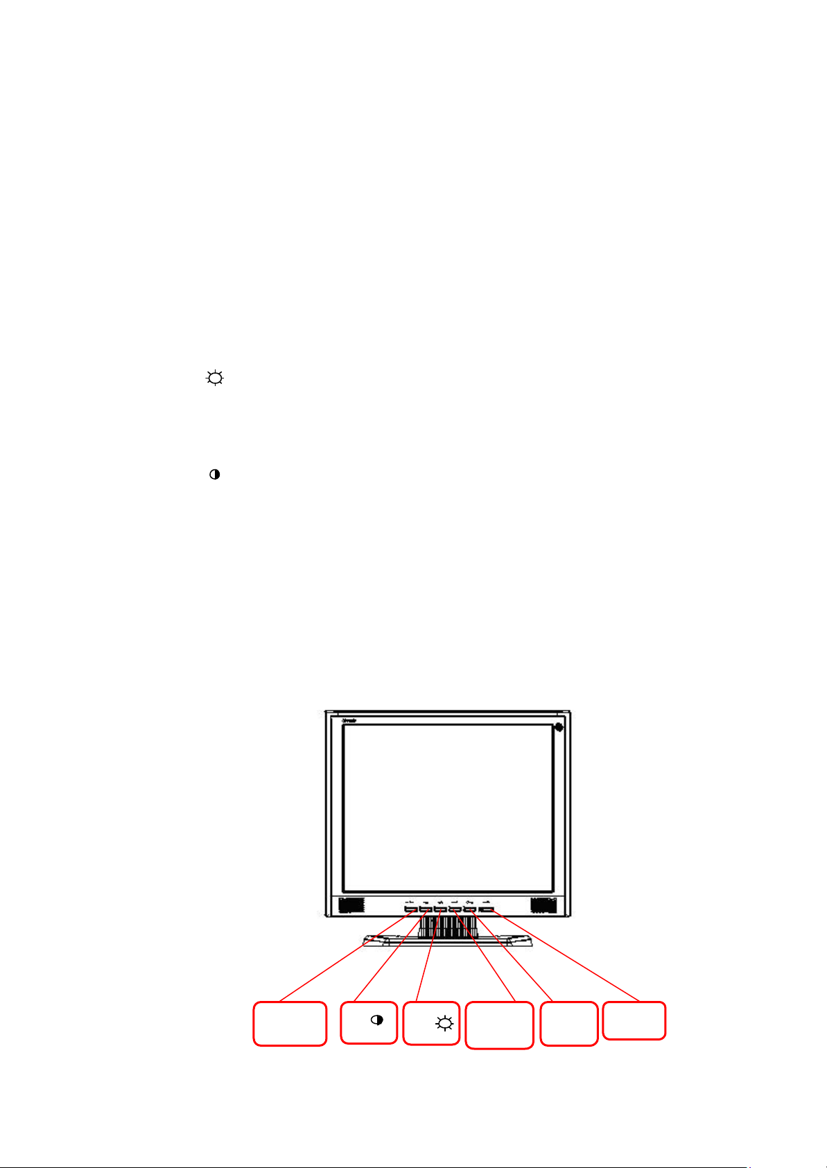
u Brightness: Press the Brightness Button when the Menu is not
displayed.
u Contrast: Press the Contrast Button when the Menu is not displayed.
u Auto Setting: Press the Auto Button when the Menu is not displayed.
u Turbo: Press the Input Button when the Menu is not displayed.
n Pct: Picture Mode (High brightness)
n Text: Text Mode (Normal)
n Eco Economy (Brightness of back-light is reduced )
n Changing to a lower brightness mode can lessen eye fatigue.
n Change from Picture Mode to Text Mode when working with text.
n Change from Text Mode to Economy Modes when viewing the
screen for long periods.
16
Page 17

2.6 Plug and Play
u The new VESA Plug and Play function is used which eliminates the
complicated and time-consuming installation process.
u You can use the Plug and Play system without encountering usual
installation problems. Your computer system can easily identify and
automatically adjust the monitor.
u The LCD Monitor uses Display Data Channel (DDC) to send
Extended Display Identification Data (EDID) to the computer
system, so the computer system can be set to monitor auto adjust.
2.7 Power Saver
u Power control system, also called (Power Saver), is installed inside
the LCD Monitor.
u If the monitor has not been used for a certain period of time, the
system will turn the monitor to low voltage mode to save power. Slight
moving or any click will return to th e original image.
u The VGA card inside the computer handles Power Saver. You can
use computer software to set the function.
u The LCD Monitor is compatible with EPA ENERGY STAR and
NÜ TEK if used with a VESA DPMS computer.
u To save power, turn off the power of the LCD monitor when not in use.
17
Page 18

MACHINE DISASSEMBLY
AND ASSEMBLY
3.1 Disassembly Procedures
Picture Description
Chapter 3
Push the hooks and stand bottom away
Remove Hinge Cover
Loosen and remove 6 screws to remove Stand Assy
Loose and remove 2 screws.
18
Separate Bezel hooks to take Bezel and Rear Cover
apart.
Lift up Rear Cover
Remove the Tinfoil
Page 19

Remove FFC
Loose and remove screw and remove Cover-FFC
Loose and remove 2 screws
Loose and remove 5 screws
Remove the Cover of X-PCB
Remove 4 pieces of Backlight wires.
Loose and remove 4 screws
Remove Power PCBA
19
Page 20

Remove 2 pieces of FFC from AD PCBA
Loose and remove 1 screw
Remove AD PCBA
Disassembly PCBA complete.
Loose an d remove 4 crews
Lift up LCD module and remove bezel.
Remove FFC.
Separate both Audio Cable.
20
Page 21

Loose and remove 3 screws.
Take OSD PCBA apart
3.2 Assembly Procedures
Place OSD PCBA.
Fasten 3 screws
Insert Audit Cable to connectors of OSD PCBA
Bezel assembly complete.
Insert FFC.
21
Page 22

Place LCD module.
Fasten 4 fixed screws
Insert new AD PCBA
Insert 2 pieces of FFC to AD PCBA
. Insert new Power PCBA
Fasten 4 fixed screws of Power PCBA
Insert 4 pieces of Backlight wires
22
Fasten 5 screws
Page 23

Join the cover hooks of X-PCB and fasten the screw
Fasten 2 screws
Place Cover-FFC and fasten screw
Insert FFC
Attach the Tinfoil
Place Rear Cover
Join hooks of Rear Cover
with Bezel
Fasten 2 screws
23
Page 24

Place Stand Assy.
Fasten 6 screws
Insert Stand Cover
Have the hook latched
24
Page 25

Troubleshooting
4.1 Abnormal Display Troubleshooting
Chapter 4
25
Page 26

26
Page 27

4.2 Abnormal (ON/OFF, LCD display, Keyboard ) Troubleshooting
27
Page 28

4.3 Abnormal (BIOS, OSD, Other Display ) Troubleshooting
28
Page 29

4.4 Audio Abnormal Troubleshooting
29
Page 30

OSD Key
DC -19V
DC/D
Main
Inverter
Backlight
LCD
D-sub
DVI
-D
3.3V
Signal
Audio In
Speaker
Audio
Connector Information
5.1 Function Block Diagram
Digital Video
Analog Video
DC-19V
Chapter 5
30
Page 31

5.2 Connector Location
31
Page 32

5.3 D-sub Mini 15pin Connector
Pin No.
1 Red video input 9 NC
2 Green video input 10 Ground
3 Blue video input 11 No connection
4 NC 12 DDC data
5 Ground 13 Horizontal sync (Composite sync)
6 Red video ground 14 Vertical sync
7 Green video ground 15 DDC clock
8 Blue video ground
Pin Function Pin No.
Pin Function
5.4 DC Connector DC Power Jack, d=3.0mm
5.5 Audio Connector (Optional) Phone Jack, d=3.5mm
5.6 Main Board Pin Assignment Introduction
5.6.1 CN-B Pin Assignment
Pin No. Symbol Description
1
2
3
4
5
6
7
8
INV_EN Inverter enable
INV_ADJ Brightness Adjustment
GND Ground
GND Ground
VIN_19V Input source
GND Ground
VIN_19V Input source
VIN_19V Input source
32
Page 33

5.6.2 CN-A1 Pin Assignment
Pin No. Symbol Description
1
2
3
4
5
6
7
8
9
10
11
12
13
14
15
16
17
18
19
20
21
22
23
24
25
26
27
28
29
30
31
32
33
34
35
36
37
38
VCOM PANEL COMMOM VOLTAGE
VCOM PANEL COMMOM VOLTAGE
VCOM PANEL COMMOM VOLTAGE
VCOM PANEL COMMOM VOLTAGE
GND GROUND
ESTH EVEN PATH STAR PULSE
GND GROUND
EB2P EVEN PATH BLUE DATA BIT
EB2N EVEN PATH BLUE DATA BIT
EB1P EVEN PATH BLUE DATA BIT
EB1N EVEN PATH BLUE DATA BIT
EB0P EVEN PATH BLUE DATA BIT
EB0N EVEN PATH BLUE DATA BIT
GND GROUND
EG2P EVEN PATH GREEN DATA BIT
EG2N EVEN PATH GREEN DATA BIT
EG1P EVEN PATH GREEN DATA BIT
EG1N EVEN PATH GREEN DATA BIT
EG0P EVEN PATH GREEN DATA BIT
EG0N EVEN PATH GREEN DATA BIT
GND GROUND
GMA10 GAMMA VOLTAGE
GMA9 GAMMA VOLTAGE
GMA8 GAMMA VOLTAGE
GMA7 GAMMA VOLTAGE
GMA6 GAMMA VOLTAGE
VSA DATA IC VOLTAGE
VSA DATA IC VOLTAG E
VSA DATA IC VOLTAGE
VSA DATA IC VOLTAGE
GMA5 GAMMA VOLTAGE
GMA4 GAMMA VOLTAGE
GMA3 GAMMA VOLTAGE
GMA2 GAMMA VOLTAGE
GMA1 GAMMA VOLTAGE
GND GROUND
ECLKP EVEN PATH CLOCK
ECLKN EVEN PATH CLOCK
33
Page 34

39
40
41
42
43
44
45
GND GROUND
ER2P EVEN PATH RED DATA BIT
ER2N EVEN PATH RED DATA BIT
ER1P EVEN PATH RED DATA BIT
ER1N EVEN PATH RED DATA BIT
ER0P EVEN PATH RED DATA BIT
ER0N EVEN PATH RED DATA BIT
5.6.3 CN-A2 Pin Assignment
Pin No. Symbol Description
1
2
3
4
5
6
7
8
9
10
11
12
13
14
15
16
17
18
19
20
21
22
23
24
25
26
27
28
NC NC
NC NC
NC NC
VGD SCAN IC VOLTAGE
VGD SCAN IC VOLTAGE
PANEL_VGL PANEL DRIVING VOLTAGE
PANEL_VGL PANEL DRIVING VOLTAGE
PANEL_VHL PANEL DRIVING VOLTAGE
PANEL_VHL PANEL DRIVING VOLTAGE
GVOFF TIMING CONTROL PIN
XAO TIMING CONTROL PIN
STV SCAN IC START PULSE
CKV SCAN IC CLOCK
OE SCAN DATA OUTPUT ENABLE
OB2P ODD PATH BLUE DATA BIT
OB2N ODD PATH BLUE DATA BIT
OB1P ODD PATH BLUE DATA BIT
OB1N ODD PATH BLUE DATA BIT
OB0P ODD PATH BLUE DATA BIT
OB0N ODD PATH BLUE DATA BIT
GND GROUND
OG2P ODD PATH GREEN DATA BIT
OG2N ODD PATH GREEN DATA BIT
OG1P ODD PATH GREEN DATA BIT
OG1N ODD PATH GREEN DATA BIT
OG0P ODD PATH GREEN DATA BIT
OG0N ODD PATH GREEN DATA BIT
GND GROUND
34
Page 35

29
30
31
32
33
34
35
36
37
38
39
40
41
42
43
44
45
OCLKP ODD PATH CLOCK
OCLKN ODD PATH CLOCK
GND GROUND
STB DATA LATCH
POL POLARITH INVERTING
GND GROUND
OR2P ODD PATH RED DATA BIT
OR2N ODD PATH RED DATA BIT
OR1P ODD PATH RED DATA BIT
OR1N ODD PATH RED DATA BIT
OR0P ODD PATH RED DATA BIT
OR0N ODD PATH RED DATA BIT
OSTH ODD PATH STAR PULSE
GND GROUND
VSD DATA IC VOLTAGE
VSD DATA IC VOLTAGE
VSD DATA IC VOLTAGE
5.6.4 CN-C Pin Assignment
Pin No. Symbol Description
1 GND GROUND
2 GND GROUND
3 GND GROUND
4 AUDIO/L- AUDIO OUTPUT
5 AUDIO/L+ AUDIO OUTPUT
6 AUDIO/R- AUDIO OUTPUT
7 AUDIO/R+ AUDIO OUTPUT
8 PWR_SW POWER KEY
9 LED_O ORANGE LED
10 LED_G GREEN LED
11 AUTO_ADJ AUTO ADJUSTMENT
12 SOURCE_SEL
INPUT SOURCE SELECTION
13 KEY_UP UP KEY
14 KEY_DOWN DOWN KEY
15 MENU MENU KEY
35
Page 36

5.6.5 CN-E Pin Assignment
Pin No. Symbol Description
1 RIN RED INPUT
2 GIN GREEN INPUT
3 BIN BLUE INPUT
4 GND GROUND
5 GND GROUND
6 RGN RED INPUT GROUND
7 GGN GREEN INPUT GROUND
8 BGN BLUE INPUT GROUND
9 VGA_5V VGA INPUT 5V
10 GND GROUND
11 GND GROUND
12 VGA_SDA I2C
13 VGA_HS H-SYNC
14 VGA_VS V-SYNC
15 VGA_SCL I2C
36
Page 37

FRU (Field Replaceable Unit) List
Chapter 6
Part List
Picture Partname Description Vendor
Part No.
Adapter ADAPTER 3.16A 60W
3PIN UP060B1190-01B
2719060199
FUNCTION
BUTTON
BOARD
INVERTER
BOARD
Main Board AL1703 MAINBOARD
CABLES MAIN BOARD CABLE -
PCBA For A170E1T,A170E1-H01-K
DC/AC Inverter,TWS444957,2560V(min)/5mA(typ
e)
(FIRMWARE CONTROL
BOARD)
FFC 55*23MM
35A17K012
0
2714000012
35A17S022
0
3241702002
37
CABLE FUNCTION BUTTON
BOARD CABLE - FFC
180MM
3241700001
Page 38

LCD STAND
AUDIO
CABLE
18AWG,180cm,Black,JCE 32F2818004
MONITOR
CABLE
30AWG,180cm,Black,JCE 32F3018003
Picture Part name Description Vendor
Part No.
STAND
BASE
LCD
FRONT
BEZEL
ABS, Black 40A1792211
Bezel Assy 40A1729245
LCD BACK
COVER
NECK
Hinge Cover ABS Black 40A1792909
Rear Assy 40A1799909
Stand Hinge Assy,
SCREW-B,Black
40A1799217
38
Page 39

MAINBOAR
D COVER
Cover_pcb_ad,D-Sub
Only
41A1799107
FFC
Cover-FFC 41A1799102
COVER
39
Page 40

40
Page 41

Schematic Diagram
Main Board
Chapter 7
41
Page 42

42
Page 43

5
DDC_CLK
DDC_DAT
ST_DET1
10/20
B2
VGA_5V
V5A
DDC_CLK
ST_DET1
V5A_ESD
VGA
B3
V5A_ESD
V5A_ESD
V5A
ST_DET2
D D
DVI
C C
VGA_5V
ST_DET2
B5
AUDIO/L+
AUDIO/L-
AUDIO/R+
AUDIO/R-
MUTE
V5A
VOL_ADJ
AUDIO
B B
AUDIO/L+
AUDIO/LAUDIO/R+
AUDIO/RMUTE
onBACKLITE
VGH
VGL
VAA
onPANEL
onPANEL1
VCM_PWM
B6
onPANEL
onBACKLITE
VGH
VGL
VAA
V5A
XAO
B4
VGA_5V
DDC_CLK
DDC_DAT
ST_DET1
ST_DET2
AudioL+
AudioLAudioR+
AudioRMUTE
V5A
onBACKLITE
onPANEL
onPANEL1
VCM_PWM
XAO
MPU
VOL_ADJ
AdjBACKLITE
GNDR
GIN
GNDG
SOG
BIN
GNDBDDC_DAT
HSYNC
VSYNC
CLK+
CLK-
V19V
RIN
R+
R-
G+
G-
B+
B-
R1 0603/390R/1%R1 0603/390R/1%
VDVI
C129NCC129
NC
CSZ
SCL
SDA
HWRESET
INT
AD0
AD3
AD1
AD2
V19V
AdjBACKLITE
V19V
C20 0603/22P/50VC20 0603/22P/50V
XTAL14.31818
XTAL14.31818
C21 0603/22P/50VC21 0603/22P/50V
DC/DC
B7
onPANEL1
VCM_PWM
A A
V5A
VAA
V33D
GMA[1..10]
VCM
V25C
V33PV5A
VCM
V33P
POWER
V33D V25C
4
RIN
GNDR
GNDG
SOG
BIN
GNDB
HSYNC
VSYNC
R+
RG+
GB+
BCLK+
CLK-
C9
C9
0603/0.1U/25V
0603/0.1U/25V
CSZ
SCL
SDA
HWRESET
INT
AD0
AD3
AD1
AD2
Y1
Y1
C22 0603/0.1u/25vC22 0603/0.1u/25v
OPEN
OPEN
R116
R116
0603/4.7k
0603/4.7k
V5A
GMA[1..10]
R117
R117
63
62
60
59
61
58
57
37
38
40
41
43
44
46
47
49
50
52
66
67
69
71
70
32
72
30
31
77
78
73
74
33
34
3
2
6
VPLL VDPLL VPOVAD VDVI VDD
35
53
45
55
U1
U1
AVDD
RIN0
RIN0M
GIN0
GIN0M
SOGIN0
BIN0
BIN0M
HSYNC0
VSYNC0
R+
RG+
GB+
BCK+
CKREXT
REFP
REFM
ALE/CSZ
RDZ/SCL
WRZ/SDA
HWRESETZ
INT
AD0/GPO6
AD3/GPO5
AD1/EINV
AD2/OINV
PWM0
PWM1
XIN
XOUT
BYPASS
AVSS_LPLL
BUSTYPE
51
65
AVDD
AVDD_DVI
AVDD_DVI
AVDD_MPLL
AVSS56AVSS_MPLL
AVSS_PLL54AVSS_DVI42GNDP10GNDP20GNDP85GNDP95GNDP
AVSS
AVSS
36
64
68
VDDP11VDDP21VDDP84VDDP94VDDP
AVDD_PLL
MST8116B
MST8116B
AVSS_DVI
AVSS_DVI
39
48
104
114
VDDP
126
VDDP
GNDP
105
3
117
VDDC18VDDC87VDDC97VDDC
RA1P
RA1N
RA2P
RA2N
RA3P
RA3N
GA1P
GA1N
GA2P
GA2N
GA3P
GA3N
BA1P
BA1N
BA2P
BA2N
BA3P
BA3N
CLKAP
CLKAN
RB1P
RB1N
RB2P
RB2N
RB3P
RB3N
GB1P
GB1N
GB2P
GB2N
GB3P
GB3N
BB1P
BB1N
BB2P
BB2N
BB3P
BB3N
CLKBP
CLKBN
ESP
OSP
GPO0
GPO1
GPO2
GPO3
GPO4
DDC1_DAT/GPO7
DDC1_CLK/GPO8
GNDP
GNDC19GNDC86GNDC
96
115
127
116
NC
NC
NC
NC
NC
GNDC
106
107
108
109
110
111
112
113
98
99
100
101
102
103
88
89
90
91
92
93
118
119
16
17
22
23
24
25
7
8
9
12
13
14
15
122
123
124
125
128
1
4
5
120
121
75
76
83
82
81
80
79
28
29
RA0
RA1
RA2GIN
RA3
RA4
RA5
GA0
GA1
GA2
GA3
GA4
GA5
BA0
BA1
BA2
BA3
BA4
BA5
RB0
RB1
RB2
RB3
RB4
RB5
GB0
GB1
GB2
GB3
GB4
GB5
BB0
BB1
BB2
BB3
BB4
BB5
CLKP_A
CLKN_A
CLKP_B
CLKN_B
ESTH
OSTH
GVON
STB
STV
CKV
OE
POL
GVOFF
RA[0..5]
GA[0..5]
BA[0..5]
RB[0..5]
GB[0..5]
BB[0..5]
B8
RA[0..5]
GA[0..5]
BA[0..5]
CLKP_A
CLKN_A
RB[0..5]
GB[0..5]
BB[0..5]
CLKP_B
CLKN_B
ESTH
OSTH
GVON
STB
STV
CKV
OE
POL
GVOFF
GMA[1..10]
PANEL
XAO
VGH
VGL
VAA
VCM
V33P
2
VAD
LL121L1LL121
C1
C1
VPLL
LL121L2LL121
C4
C4
1206/10U/16V/Y5V
1206/10U/16V/Y5V
VDVI
LL121L3LL121
C6
C6
1206/10U/16V/Y5V
1206/10U/16V/Y5V
VDPLL
LL121L4LL121
C10
C10
1206/10U/16V/Y5V
1206/10U/16V/Y5V
VPO
LL121L5LL121
C12
C12
1206/10U/16V/Y5V
1206/10U/16V/Y5V
VDD
LL121L6LL121
C23
C23
1206/10U/16V/Y5V
1206/10U/16V/Y5V
0603/0.1U/25V
0603/0.1U/25V
0603/0.1U/25V
0603/0.1U/25V
V33D
V25C
V33A
L1
1206/10U/16V/Y5V
1206/10U/16V/Y5V
V33A
L2
V33A
L3
V33A
L4
V33D
L5
V25C
L6
C2
C2
C3
C3
0603/0.1U/25V
0603/0.1U/25V
0603/0.1U/25V
0603/0.1U/25V
C5
C5
0603/0.1U/25V
0603/0.1U/25V
C8
C8
C7
C7
0603/0.1U/25V
0603/0.1U/25V
0603/0.1U/25V
0603/0.1U/25V
C11
C11
0603/0.1U/25V
0603/0.1U/25V
0603/0.1U/25V
0603/0.1U/25V
C14
C14
C13
C13
C15
C15
0603/0.1U/25V
0603/0.1U/25V
C24
C24
C25
C25
C26
C26
0603/0.1U/25V
0603/0.1U/25V
0603/0.1U/25V
0603/0.1U/25V
1
C16
C16
C17
C17
0603/0.1U/25V
0603/0.1U/25V
0603/0.1U/25V
0603/0.1U/25V
C27
C27
0603/0.1U/25V
0603/0.1U/25V
0603/0.1U/25V
0603/0.1U/25V
C18
C18
C19
C19
0603/0.1U/25V
0603/0.1U/25V
5
4
3
2
1
Page 44

5
D D
V5A
L18
L18
0805/42
V5A2,3,4,5,8
C C
B B
0805/42
L19
L19
0805/42
0805/42
L20
L20
0805/42
0805/42
C108
C108
1206/22U/10V/Y5V
1206/22U/10V/Y5V
C114
C114
1206/22U/10V/Y5V
1206/22U/10V/Y5V
C121
C121
1206/22U/10V/Y5V
1206/22U/10V/Y5V
4
U9 2101117STSU9 2101117STS
3
C109
C109
0603/0.1u/25V
0603/0.1u/25V
U10 2101117STSU10 2101117STS
3
C115
C115
0603/0.1u/25V
0603/0.1u/25V
U11 2101117T3SU11 2101117T3S
3
C122
C122
0603/0.1u/25V
0603/0.1u/25V
VI(5V)
VI(5V)
VI(5V)
VO(3.3V)
VO(3.3V)
GND
1
VO(3.3V)
VO(3.3V)
GND
1
VO(3.3V)
VO(3.3V)
GND
1
V33D1 V33D1
2
4
V33A1 V33A1
2
4
V25C1 V25C1
2
4
V33D
TP
1
C110
C110
C111
C111
0603/0.1u/25V
0603/0.1u/25V
1206/22U/10V/Y5V
1206/22U/10V/Y5V
V33A
TP
1
C117
C117
C116
C116
0603/0.1u/25V
0603/0.1u/25V
1206/22U/10V/Y5V
1206/22U/10V/Y5V
V25C
TP
1
C124
C124
C123
C123
0603/0.1u/25V
0603/0.1u/25V
1206/22U/10V/Y5V
1206/22U/10V/Y5V
3
V33D 1,3
(Digital VCC)
(SCALER VCC)
V25C 1
(SCALER Core VCC)
2
V33D
C112
32
Q9
Q9
2N7002_Panjit
2N7002_Panjit
C112
0603/1n/50V
0603/1n/50V
R99
R99
0603/4.7K
0603/4.7K
0603/100R
0603/100R
R100
onPANEL15
R100
C120
C120
Open
Open
1
Q8
Q8
FDN338P
FDN338P
1
C119
C119
+
+
1206/10U/16V/Y5V
1206/10U/16V/Y5V
32
C118
C118
0603/0.1u/25V
0603/0.1u/25V
(Panel VCC)
C113
C113
+
+
1206/10U/16V/Y5V
1206/10U/16V/Y5V
1
V33P 6
BROAD PAD
A A
5
4
3
2
1
 Loading...