

Acer AL1517v Schematic

FRU (Field Replaceable Unit) List
This chapter gives you the FRU (Field Replaceable Unit) listing in global configurations of AL1517. Refer to this
chapter whenever ordering for parts to repair or for RMA (Return Merchandise Authorization).
NOTE: Please note WHEN ORDERING FRU PARTS, that you should check the most up-to-date information
available on your regional web or channel (http://aicsl.acer.com.tw/spl/). For whatever reasons a part
number change is made, it will not be noted in the printed Service Guide. For ACER AUTHORIZED
SERVICE PROVIDERS, your Acer office may have a DIFFERENT part number code from those given in
the FRU list of this printed Service Guide. You MUST use the local FRU list provided by your regional Acer
office to order FRU parts for repair and service of customer machines.
NOTE: To scrap or to return the defective parts, you should follow the local government ordinance or regulations
on how to dispose it properly, or follow the rules set by your regional Acer office on how to return it.
Chapter 6
39
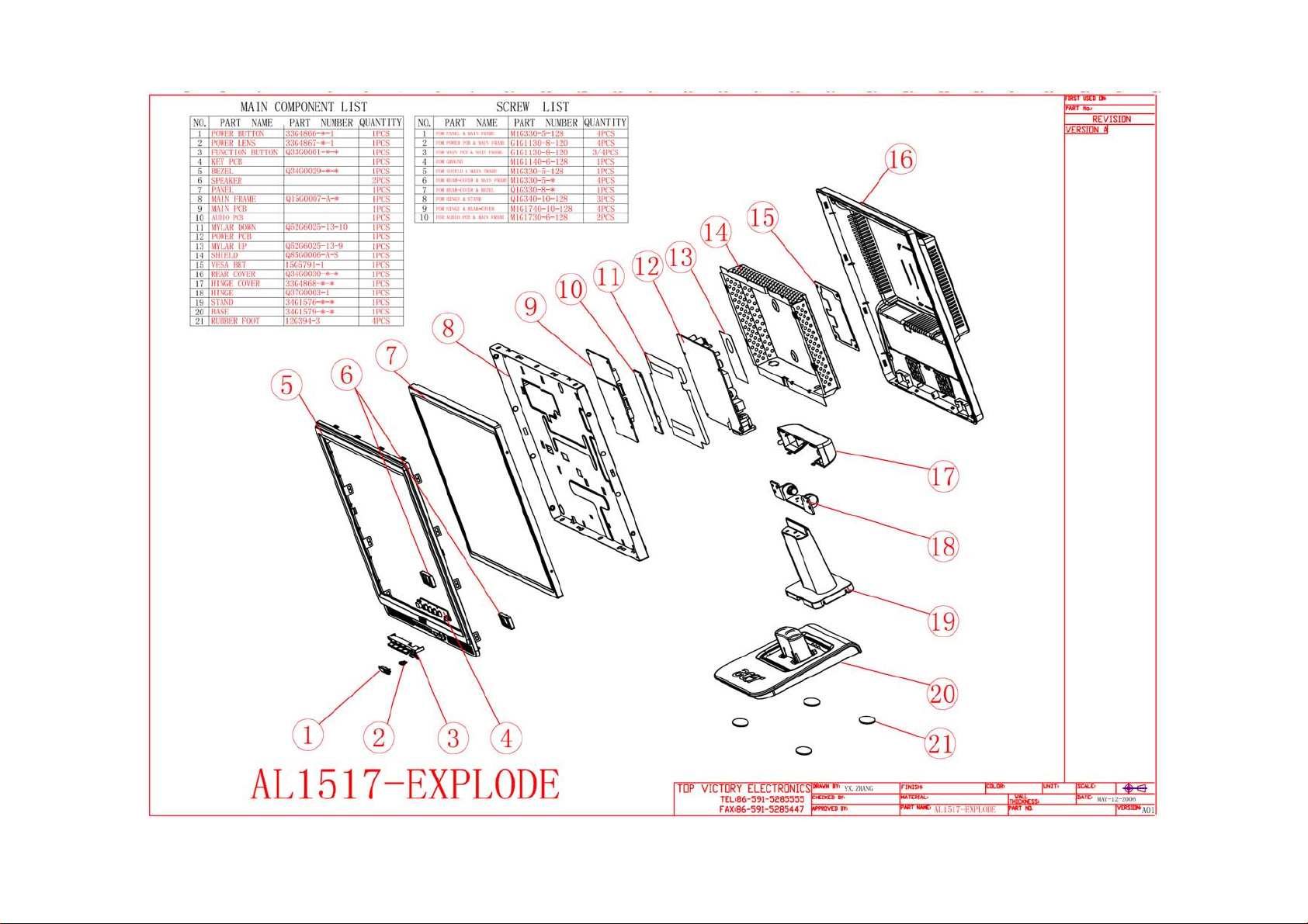
Exploded Diagram (Model: AL1517)
40
Part List
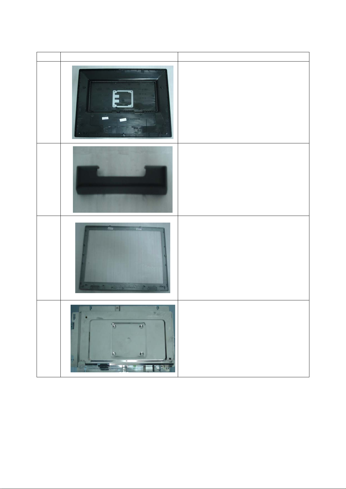
Above picture show the description of the following component.
Item Picture Description
1
2
3
Back Cover
Q34G0030 RX 1B
Hinge Cover
033G4868 RX L
Bezel
Q34G0029 QWA1B
4
Shield
Q85G0006 A S
41
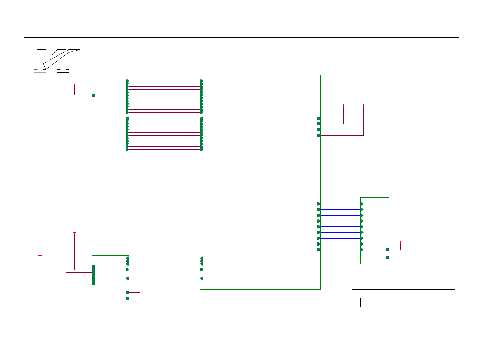
Schematic Diagram
Chapter 7
TSUM16AK SCHEMATIC
LVDS OUTPUT
VCC3.3
VCC1.8
VCC1.8
Vcc3.3
+5V
+12V
PA[0..7]
PA[8..13]
PA[14..19]
PB[0..5]
PB[6..11]
PB[12..23]
GPO[0..4]
ESP
OSP
PA[0..7]
PA[8..13]
PA[14..19]
PB[0..5]
PB[6..11]
PB[12..23]
GPO[0..4]
+12V
+5V
B5
PA[0..7]
PA[8..13]
PA[14..19]
PB[0..5]
PB[6..11]
PB[12..23]
GPO[0..4]
ESP
OSP
VLCD
VLCD_12V
VLCD
VLCD_12V
5.PANEL INTERFACE
Title
Size Document Number Rev
B
Date: Sheet
TSUM16AK
TOP
of
05Monday, May 30, 2005
A
VCC3.3
VCC5V
+5V
VCC1.8
+3V3
+5V
PC5V
+12V
B3
+5V
3.INPUT
B2
+12V
+3V3
VCC1.8
+5V
VCC5V
VCC3.3
2.POWER
GNDR
GNDG
SOG
GNDB
HSYNC
VSYNC
DDCA_SDA
DDCA_SCL
DET_VGA
DDC_WP
CLK+
CLK-
DDCD_SDA
DDCD_SCL
DET_DVI
on_BACKLIGHT
on_Panel
on_PANEL_12V
VCTRLPC5V
Adj_BACKLIGHT
VLCD
VLCD_12V
XGA/SXGA
B4
RIN
GIN
BIN
R+
R-
G+
GB+
B-
VLCD_12V
VLCD
RIN
GNDR
GIN
GNDG
SOG
BIN
GNDB
HSYNC
VSYNC
DDCA_SDA
DDCA_SCL
DET_VGA
DDC_WP
R+
RG+
GB+
BCLK+
CLKDDCD_SDA
DDCD_SCL
DET_DVI
on_BACKLIGHT
on_Panel
on_PANEL_12V
VCTRL
Adj_BACKLIGHT
4.SCALER
42
 Loading...