

Page 1

Full-size SBC FSB-B75G
FSB-B75G
Intel® CoreTM i7/i5/i3
LGA 1155 Processor
Full-size CPU Card
With DDR3, 2 Gigabit Ethernet
USB 3.0/ USB2.0, SATA 6.0Gb/s
FSB-B75G Manual Rev.A 2nd Ed.
March 2013
Page 2

Full-size SBC FSB-B75G
Copyright Notice
This document is copyrighted, 2013. All rights are reserved. The
original manufacturer reserves the right to make improvements to the
products described in this manual at any time without notice.
No part of this manual may be reproduced, copied, translated, or
transmitted in any form or by any means without the prior written
permission of the original manufacturer. Information provided in this
manual is intended to be accurate and reliable. However, the original
manufacturer assumes no responsibility for its use, or for any infringements upon the rights of third parties that may result from its
use.
The material in this document is for product information only and is
subject to change without notice. While reasonable efforts have been
made in the preparation of this document to assure its accuracy,
AAEON assumes no liabilities resulting from errors or omissions in
this document, or from the use of the information contained herein.
AAEON reserves the right to make changes in the product design
without notice to its users.
i
Page 3

Full-size SBC FSB-B75G
Acknowledgments
All other products’ name or trademarks are properties of their
respective owners.
AMI is a trademark of American Megatrends Inc.
Intel
Microsoft Windows
PC/AT, PS/2, and VGA are trademarks of International Business
All other product names or trademarks are properties of their
respective owners.
®
, Core™ are trademarks of Intel® Corporation.
®
is a registered trademark of Microsoft Corp.
Machines Corporation.
ii
Page 4

Full-size SBC FSB-B75G
Packing List
Before you begin installing your card, please make sure that the
following materials have been shipped:
1 Serial Port Cable with one DB-9 connector
1 Cable with serial port and LPT port
1 USB Cable
4 SATA Cables
1 5V & PS_ON Cable
1 DVD-ROM for manual (in PDF format) and
Drivers
1 FSB-B75G
If any of these items should be missing or damaged, please
contact your distributor or sales representative immediately.
iii
Page 5

Full-size SBC FSB-B75G
Contents
Chapter 1 General Information
1.1 Introduction................................................................ 1-2
1.2 Features....................................................................1-3
1.3 Specifications............................................................1-4
Chapter 2 Quick Installation Guide
2.1 Safety Precautions....................................................2-2
2.2 Location of Connectors and Jumpers ....................... 2-3
2.3 Mechanical Drawing..................................................2-4
2.4 List of Jumpers.......................................................... 2-5
2.5 List of Connectors ..................................................... 2-5
2.6 Setting Jumpers ........................................................ 2-7
2.7 Auto Power Button (JP2)........................................... 2-8
2.8 Clear CMOS (JP3) .................................................... 2-8
2.9 Front Panel Connector (FP1).................................... 2-8
2.10 Front Panel Connector (FP2).................................. 2-8
2.11 Digital I/O Pin Header (DIO1).................................. 2-9
2.12 USB3.0 Port Pin Header (USB1, USB5).................2-9
2.13 SPI Pin Header (CN1).............................................2-9
2.14 5V&PS_ON# Pin Header (CN2)..............................2-10
2.15 Caseopen# Pin Header (CN6)................................2-10
2.16 PS2 KB/MS Pin Header (CN7)................................ 2-10
Chapter 3 AMI BIOS Setup
iv
Page 6

Full-size SBC FSB-B75G
3.1 System Test and Initialization. .................................. 3-2
3.2 AMI BIOS Setup........................................................3-3
Chapter 4 Driver Installation
4.1 Installation.................................................................4-3
Appendix A Programming The Watchdog Timer
A.1 Programming .........................................................A-2
A.2 W83627DHG Watchdog Timer Initial Program......A-6
Appendix B I/O Information
B.1 I/O Address Map....................................................B-2
st
B.2 1
MB Memory Address Map ................................B-4
B.3 IRQ Mapping Chart................................................B-5
B.4 DMA Channel Assignments...................................B-8
Appendix C Mating Connector
C.1 List of Mating Connectors and Cables.................. C-2
Appendix D AHCI Settings
D.1 Setting AHCI......................................................... D-2
v
Page 7

Full-size SBC FSB-B75G
Chapter
1
General
Information
Chapter 1 General Information 1-1
Page 8

Full-size SBC FSB-B75G
1.1 Introduction
AAEON, a leading Industrial PC manufacturer, announces the
debut of a high performance full-size Single Board Computer, the
FSB-B75G.
latest Intel
AAEON has developed this full-size SBC based on the
®
B75 chipset and the Intel® 3rd generation Core™i7/i5/i3
LGA 1155 processor, to fulfill the increasing demands of multi-core
processing.
In a PICMG 1.0 form factor, the FSB-B75G system host board t akes
®
full advantage of the Intel
B75 chipset for enhanced system
performance and generous expansion capabilities. Considerable
bandwidth is available with point-to-point serial PCI-Express via
[x16] and [x4] interfaces. Maximizing the available PCI-Express
channels offers the greatest flexibility to today’ s d ema nding I/O
requirements. Two DIMM slots of dual-channel DDR3 1333/1600
sockets provide ample memory bus bandwidth for demanding
applications. The FSB-B75G has been designed for users that
require high performance and reliability for critical applications.
Chapter 1 General Information 1-2
Page 9

Full-size SBC FSB-B75G
1.2 Features
Intel
Intel
Dual-Channel DDR3 1333/1600 DIMM Socket x 2 (Up to
® 3rd
Generation CoreTM i7/i5/i3 LGA 1155 Processor
®
B75 Chipset
16 GB)
Intel
Gigabit Ethernet x 2
SATA 6.0 Gb/s x 1, SA TA 3.0 Gb/s x 2, CFast™ x 1
®
B75 Integrated Intel® HD Graphics
(Optional)
USB3.0 x 4, USB2.0 x 6, COM x 2, LPT x 1
Compliance with PICMG 1.0
ATX 2.1 Power Requirement
Chapter 1 General Information 1-3
Page 10

Full-size SBC FSB-B75G
1.3 Specification
System
Form Factor PICMG 1.0 Full size SBC
Processor Intel® 3rd Generation CoreTM i7/i5/i3 LGA
1155 Processor
System Memory 240-pin Dual-Channel DDR3 1333/1600
DIMM socket x 2, up to 16GB
Chipset Intel® B75
I/O Chipset Winbond W83627DHG-P
Ethernet Realtek 8111E, 10/100/ 1000Base-TX,
RJ-45 x 2 on bracket
BIOS AMI Plug & Play SPI BIOS-128MB ROM
Wake on LAN Yes
Watchdog Timer 1~255 steps by software programming
H/W Status Monitoring System temperature, voltage and cooling
fan status monitoring
Expansion Interface Follows PICMG 1.0 Regulation
Battery Lithium battery
Power Requirement ATX 2.1
Board Size 13.3” x 5” (339mm x 126mm)
Gross Weight 1.2 lb (0.5 Kg)
Operating
32oF ~ 140 oF (0oC ~ 60 oC)
Temperature
o
Storage Temperature -4
Chapter 1 General Information 1-4
F ~ 158 oF (-20oC ~ 70 oC)
Page 11

Full-size SBC FSB-B75G
Operating Humidity 5%~90% resistive humidity,
non-condensing
Display
Chipset Intel® B75
Graphic Engine Integrated Intel® HD Graphics
Resolution Up to 2048x1536 @ 75Hz for CRT
Output Interface VGA x 1 on bracket
I/O
Storage SATA 6.0 Gb/s x 1, SATA 3.0 Gb/s x 2,
CFast
™ x 1 (optional)
Serial Port COM x 2
COM1: RS-232 with box header
COM2: RS-232/422/485 with box header
PS/2 Port Keyboard/Mouse x 1 (4x2 pin header)
USB USB3.0 x 4 (Internal 10x2 pin header x 2)
USB2.0 x 6 (onboard dual type-A
connector x 2, internal 5x2 pin header x
2)
Parallel Port LPT port x 1
Audio HDAC daughter board (optional) Mic-in/
Line-in/ Line-out/ CD-in
Chapter 1 General Information 1-5
Page 12

Full-size SBC FSB-B75G
Chapter
2
Quick
Inst
Chapter 2 Quick Installation Guide 2 - 1
allation
Guide
Page 13
Full-size SBC FSB-B75G
2.1 Safety Precautions
Always completely disconnect the power cord
from your board whenever you are working on
it. Do not make connections while the power is
on, because a sudden rush of power can
damage sensitive electronic components.
Always ground yourself to remove any static
charge before touching the board. Modern
electronic devices are very sensitive to static
electric charges. Use a grounding wrist strap at
all times. Place all electronic components on a
static-dissipative surface or in a static-shielded
bag when they are not in the chassis
Chapter 2 Quick Installation Guide 2 - 2
Page 14
Full-size SBC FSB-B75G
2.2 Location of Connectors and Jumpers
Chapter 2 Quick Installation Guide 2 - 3
Page 15
Full-size SBC FSB-B75G
2.3 Mechanical Drawing
Chapter 2 Quick Installation Guide 2 - 4
Page 16

Full-size SBC FSB-B75G
2.4 List of Jumpers
The board has a number of jumpers that allow you to configure your
system to suit your application.
The table below shows the function of each of the board's jumpers:
Jumpers
Label Function
JP2 AUTO POWER BUTTOM
JP3 Clear CMOS
2.5 List of Connectors
The board has a number of connectors that allow you to configure
your system to suit your application. The table below shows the
function of each board's connectors:
Label Function
FP1 Front Panel Connector 1
FP2 Front Panel Connector 2
CN1 SPI Pin Header
CN2 5V&PS_ON# Pin Header
CN6 Case open Pin Header
CN7 PS2 KB/MS Pin Header
CN3 Audio Pin Header
COM1 RS-232 Pin Header
COM2 RS-232/422/485 Pin Header
Chapter 2 Quick Installation Guide 2 - 5
Page 17

Full-size SBC FSB-B75G
DIO1 Digital I/O Pin Header
FDD1 Floppy Pin Header
LPT1 Parallel Port Pin Header
USB1 USB 3.0 Pin Header
USB5 USB 3.0 Pin Header
USB2 USB Pin Header
USB3 USB Pin Header
USB4 USB Connector
USB6 USB Connector
BT1 Battery
SATA1~SATA3 SATA Connector
LAN1
LAN2
10/100/1000 Base Ethernet Connector
10/100/1000 Base Ethernet Connector
DIMM1 DDR3 DIMM Slot
DIMM2 DDR3 DIMM Slot
CPU_FAN 4 Pin Fan Connector
SYS_FAN 4 Pin Fan Connector
VGA1 VGA Connector
Chapter 2 Quick Installation Guide 2 - 6
Page 18
Full-size SBC FSB-B75G
2.6 Setting Jumpers
You configure your card to match the needs of your application by
setting jumpers. A jumper is the simplest kind of electric switch. It
consists of two metal pins and a small metal clip (oft en protected by
a plastic cover) that slides over the pins to connect them. To “close”
a jumper you connect the pins with the clip.
To “open” a jumper you remove the clip. Sometimes a jumper will
have three pins, labeled 1, 2 and 3. In this case you would connect
either pins 1 and 2 or 2 and 3.
3
2
1
Open Closed Cl osed 2-3
A pair of needle-nose pliers may be helpful when working with
jumpers.
If you have any doubts about the best hardware configuration for
your application, contact your local distributor or sales
representative before you make any change.
Generally, you simply need a standard cable to make most
connections.
Chapter 2 Quick Installation Guide 2 - 7
Page 19

Full-size SBC FSB-B75G
2.7 Auto Power Button (JP2)
JP2 Function
1-2 Power ON by Button (default)
2-3 Auto Power ON
2.8 Clear CMOS (JP3)
JP3 Function
1-2 Protected (default)
2-3 Clear
2.9 Front Panel Connector (FP1)
Pin Signal Pin Signal
1 Power On Button (+) 2 Reset Switch (+)
3 Power On Button (-) 4 Reset Switch (-)
5 HDD LED (+) 6 Power LED (+)
7 HDD LED (-) 8 Power LED (-)
2.10 Front Panel Connector (FP2)
Pin Signal Pin Signal
1 External Speaker (+) 2 Key Board Lock (+)
3 NC 4 GND
5 Internal Buzzer (-) 6 I2C Bus SMB Clock
7 External Speaker (-) 8 I2C Bus SMB Data
Note: Closed Pin 5, 7: Internal Buzzer Enable
Chapter 2 Quick Installation Guide 2 - 8
Page 20

Full-size SBC FSB-B75G
2.11 Digital I/O Pin Header (DIO1)
Pin Signal Pin Signal
1 DIO_30 2 DIO_31
3 DIO_32 4 DIO_33
5 DIO_34 6 DIO_35
7 DIO_36 8 DIO_37
9 +5V 10 GND
2.12 USB3.0 Port Pin Header (USB1, USB5)
Pin Signal Pin Signal
1 VCC 20 NC
2 USB3_RX1_DN_C 19 VCC
3 USB3_RX1_DP_C 18 USB3_RX2_DN_C
4 GND 17 USB3_RX2_DP_C
5 USB3_TX1_DN_C 16 GND
6 USB3_TX1_DP_C 15 USB3_TX2_DN_C
7 GND 14 USB3_TX2_DP_C
8 USBP_0N_C 13 GND
9 USBP_0P_C 12 USBP_1N_C
10 NC 11 USBP_1P_C
2.13 SPI Pin Header (CN1)
Pin Signal Pin Signal
1 3.3V_SPI 2 GND
3 SPI_CS0 4 SPI_CLK
5 SPI_SO 6 SPI_SI
7 HOLD 8 NC
Chapter 2 Quick Installation Guide 2 - 9
Page 21

Full-size SBC FSB-B75G
2.14 5V&PS_ON# Pin Header (CN2)
Pin Signal Pin Signal
1 PS_ON# 2 +5V
3 5VSB
2.15 Caseopen# Pin Header (CN6)
Pin Signal Pin Signal
1 Case open# 2 GND
2.16 PS2 KB/MS Pin Header (CN7)
Pin Signal Pin Signal
1
3
5
7
KBDATA
GND
MSDATA
NC
2
KBCLK
4
+5V
6
MSCLK
8
NC
Remarks:
The FSB-B75G is designed for ATX system only. When used in AT
system, the 5VSB and PSON should be connected by a 3-pin power
cable (1703030501, including in accessory bag) to short 1-3 pin.
Chapter 2 Quick Installation Guide 2 - 10
Page 22

Full-size SBC FSB-B75G
Below Table for China RoHS Requirements
产品中有毒有害物质或元素名称及含量
AAEON Main Board/ Daughter Board/ Backplane
有毒有害物质或元素
部件名称
铅
(Pb)汞 (Hg)镉 (Cd)
六价铬
(Cr(VI))
多溴联苯
(PBB)
多溴二苯醚
(PBDE)
印刷电路板
× ○ ○ ○ ○ ○
及其电子组件
外部信号
× ○ ○ ○ ○ ○
连接器及线材
O:表示该有毒有害物质在该部件所有均质材料中的含量均在
SJ/T 11363-2006 标准规定的限量要求以下。
X:表示该有毒有害物质至少在该部件的某一均质材料中的含量超出
SJ/T 11363-2006 标准规定的限量要求。
备注:此产品所标示之环保使用期限,系指在一般正常使用状况下。
Chapter 2 Quick Installation Guide 2 - 11
Page 23

Full-size SBC FSB-B75G
Chapter
3
AMI
BIOS Setup
Chapter 3 AMI BIOS Setup 3-1
Page 24

Full-size SBC FSB-B75G
3.1 System Test and Iinitialization
These routines test and initialize board hardware. If the routines
encounter an error during the tests, you will either hear a few short
beeps or see an error message on the screen. There are two kinds
of errors: fatal and non-fatal. The system can usually continue the
boot up sequence with non-fatal errors.
System configuration verification
These routines check the current system configuration stored in the
CMOS memory and BIOS NVRAM. If system configuration is not
found or system configuration data error is detected, system will
load optimized default and re-boot with this default system
configuration automatically.
There are four situations in which you will need to setup system
configuration:
1. You are starting your system for the first time
2. You have changed the hardware att ached to your system
3. The system configuration is reset by Clear-CMOS jumper
4. The CMOS memory has lost power and the configuration
information has been erased.
The FSB-B75G CMOS memory has an integral lithium battery
backup for data retention. However, you will need to replace the
complete unit when it finally runs down.
Chapter 3 AMI BIOS Setup 3-2
Page 25

Full-size SBC FSB-B75G
3.2 AMI BIOS Setup
AMI BIOS ROM has a built-in Setup program that allows users to
modify the basic system configuration. This type of information is
stored in battery-backed CMOS RAM and BIOS NVRAM so that it
retains the Setup information when the power is turned off.
Entering Setup
Power on the computer and press <Del>or <F2> immediately. This
will allow you to enter Setup.
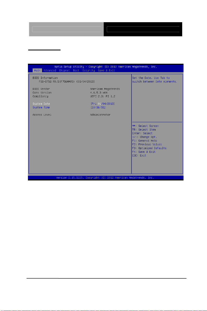
Main
Set the date, use tab to switch between date elements.
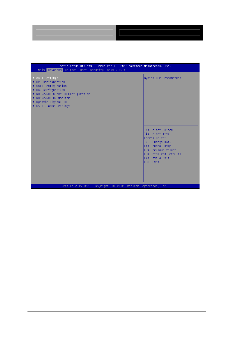
Advanced
Enable disable boot option for legacy network devices.
Chipset
Host bridge parameters.
Boot
Enables/disable quiet boot option.
Security
Set setup administrator password.
Save & Exit
Exit system setup after saving the changes.
Chapter 3 AMI BIOS Setup 3-3
Page 26
Full-size SBC FSB-B75G
Setup Menu
Setup submenu: Main
Chapter 3 AMI BIOS Setup 3-4
Page 27
Full-size SBC FSB-B75G
Setup submenu: Advanced
Chapter 3 AMI BIOS Setup 3-5
Page 28
Full-size SBC FSB-B75G
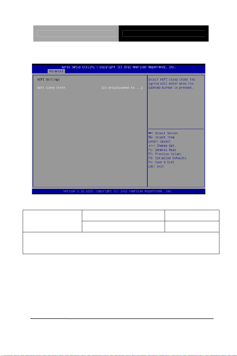
ACPI Settings
Options Summary :
ACPI Sleep State
Select ACPI sleep state the system will enter when the SUSPEND button is
pressed.
Chapter 3 AMI BIOS Setup 3-6
S1 Only (CPU Stop Clock)
S3 Only (Suspend to RAM) Default
Page 29
Full-size SBC FSB-B75G
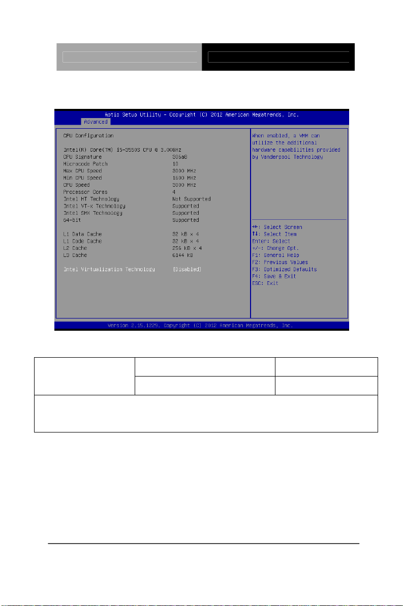
CPU Configuration
Options Summary :
Intel Virtualization
Technology
When enabled, a VMM can utilize the additional hardware capabilities provided by
Vander pool Technology
Disabled Default
Enabled
Chapter 3 AMI BIOS Setup 3-7
Page 30

Full-size SBC FSB-B75G
SATA Configuration (IDE)
Chapter 3 AMI BIOS Setup 3-8
Page 31

Full-size SBC FSB-B75G
SATA Configuration (AHCI)
Options summary :
SATA Controller(s)
Enable or disable SATA device.
Determines how SATA controller(s) operate.
Enabled Default
Disabled
IDE Default SATA Mode Selection
AHCI
Chapter 3 AMI BIOS Setup 3-9
Page 32

Full-size SBC FSB-B75G
USB Configuration
Options summary :
Legacy USB Support
Enable Legacy USB support. Auto option disables legacy support if no USB
devices are connected. DISABLE option will keep USB devices available only
for EFI applications.
Enable/Disable USB3.0 (XHCI) Controller support.
Chapter 3 AMI BIOS Setup 3-10
Enabled Default
Disabled
Auto
Enabled Default USB3.0 Support
Disabled
Page 33

Full-size SBC FSB-B75G
W83627DHG Super IO Configuration
Options Summary :
Floppy Disk Controller
Configuration
Serial Port 1 Configuration Set Parameters of Serial Port 1 (COMA)
Serial Port 2 Configuration Set Parameters of Serial Port 2 (COMB)
Parallel Port Configuration Set Parameters of Parallel Port (LPT/LPTE)
Restore AC Power Loss
Select AC power state when power is re-applied after a power failure.
Set Parameters of Floppy Disk Controller
(FDC)
Always OFF
Always ON
Last State Default
Chapter 3 AMI BIOS Setup 3-11
Page 34

Full-size SBC FSB-B75G
Floppy Disk Controller Configuration
Options Summary :
Floppy Disk Controller
Enable or Disable Floppy Disk Controller
Chapter 3 AMI BIOS Setup 3-12
Disabled
Enabled Default
Page 35

Full-size SBC FSB-B75G
Serial Port 1 Configuration
Options Summary :
Serial Port
Enable or Disable Serial Port (COM)
Change Settings
Select an optimal setting for Super IO device.
Disabled
Enabled Default
Auto Default
IO=3F8h; IRQ=4
IO=2F8h; IRQ=3
Chapter 3 AMI BIOS Setup 3-13
Page 36

Full-size SBC FSB-B75G
Serial Port 2 Configuration
Options Summary :
Serial Port
Enable or Disable Serial Port (COM)
Change Settings
Select an optimal setting for Super IO device.
Chapter 3 AMI BIOS Setup 3-14
Disabled
Enabled Default
Auto Default
IO=2F8h; IRQ=3
IO=3F8h; IRQ=4
RS232 Default RS232/422,485
RS422
Page 37

Full-size SBC FSB-B75G
RS232/422,485 switch
Parallel Port Configuration
RS485
Options Summary :
Parallel Port
Enable or Disable Parallel Port (LPT/LPTE)
Disabled
Enabled Default
Auto Default Change Settings
IO=378h; IRQ=5
Chapter 3 AMI BIOS Setup 3-15
Page 38

Full-size SBC FSB-B75G
IO=378h;
IRQ=5,6,7,10,11,12
IO=278h;
IRQ=5,6,7,10,11,12
IO=3BCh;
IRQ=5,6,7,10,11,12
Select an optimal setting for Super IO device.
Device Mode
Change the Printer Port mode.
STD Printer Mode Default
SPP Mode
EPP-1.9 and SPP Mode
EPP-1.7 and SPP Mode
ECP Mode
ECP and EPP 1.9 Mode
ECP and EPP 1.7 Mode
Chapter 3 AMI BIOS Setup 3-16
Page 39

Full-size SBC FSB-B75G
W83627DHG HW Monitor
Options Summary :
Smart Fan Function
Enable or Disable Smart Fan
Smart Fan Mode Configuration Smart Fan Mode Select
Disabled
Enabled Default
Chapter 3 AMI BIOS Setup 3-17
Page 40

Full-size SBC FSB-B75G
Smart Fan Mode Configuration
Options Summary :
SYS Smart Fan Mode
SYS Smart Fan Mode Select
SYSFAN PWM/DC Voltage Output 0~255 Default : 255
Input expect PWM Output Value(Range:0 – 255)
Chapter 3 AMI BIOS Setup 3-18
Manual Mode Default
Thermal Cruise Mode
Fan Speed Cruise
Mode
Manual Mode Default CPU Smart Fan 0 Mode
Thermal Cruise Mode
Page 41

Full-size SBC FSB-B75G
CPU Smart Fan 0 Mode Select
Fan Speed Cruise
Mode
SMART FAN III Mode
CPUFAN0 PWM/DC Voltage
Output
Input expect PWM Output Value(Range: 0 – 255)
It’s also the Fan Output initial value in Smart Fan III Mode
FAN Step down Time Time Default : 10
FAN Step down time value, unit is 0.1, default is 1 second
FAN Step up Time Time Default: 10
FAN Step up time
0~255 Default : 255
Chapter 3 AMI BIOS Setup 3-19
Page 42

Full-size SBC FSB-B75G
Dynamic Digital IO( Default Disabled)
Chapter 3 AMI BIOS Setup 3-20
Page 43

Full-size SBC FSB-B75G
Dynamic Digital IO(Enabled)
Options Summary :
Dynamic Digital IO Configuration Dynamic Digital IO Configuration
Chapter 3 AMI BIOS Setup 3-21
Page 44

Full-size SBC FSB-B75G
Dynamic Digital IO Configuration
Options Summary :
DIO0 Direction
Set Digital IO as Input or Output
Set Digital IO as Input or Output
Set Digital IO as Input or Output
Chapter 3 AMI BIOS Setup 3-22
Input Default
Output
Input Default DIO1 Direction
Output
Input Default DIO2 Direction
Output
Page 45

Full-size SBC FSB-B75G
Set Digital IO as Input or Output
Set Digital IO as Input or Output
Set Digital IO as Input or Output
Set Digital IO as Input or Output
Input Default DIO3 Direction
Output
Input DIO4 Direction
Output Default
Input DIO5 Direction
Output Default
Input DIO6 Direction
Output Default
Input DIO7 Direction
Output Default
Set Digital IO as Input or Output
Set Digital IO Output as Hi or Low
Hi Default Output Level
Low
Chapter 3 AMI BIOS Setup 3-23
Page 46

Full-size SBC FSB-B75G
S5 RTC Wake Settings
Options Summary :
Wake system with Fixed Time
Enable or disable System wake on alarm event. When enabled, System will wake
on the hr::min::sec specified
Enable or disable System wake on alarm event. When enabled, System will wake
on the hr::min::sec specified
Chapter 3 AMI BIOS Setup 3-24
Disabled Default
Enabled
Disabled Default Wake system with Dynamic Time
Enabled
Page 47

Full-size SBC FSB-B75G
Setup submenu: Chipset
Options Summary :
System Agent (SA) Configuration System Agent (SA) Parameters
PCH-IO Configuration PCH Parameters
Chapter 3 AMI BIOS Setup 3-25
Page 48

Full-size SBC FSB-B75G
System Agent (SA) Configuration
Options Summary :
Graphics Configuration Configure PEGO B0:D1:F0 Fen1-Gen3
Chapter 3 AMI BIOS Setup 3-26
Page 49

Full-size SBC FSB-B75G
Graphics Configuration
Options Summary :
Primary Display
Select which of IGFX/PEG/PCI Graphics device should be Primary Display Or
select SG for Switchable Gfx.
Internal Graphics
Auto Default
IGFX
PEG
PCI
Auto
Disabled
Enabled
Chapter 3 AMI BIOS Setup 3-27
Page 50

Full-size SBC FSB-B75G
Keep IGD enabled based on the setup options.
DVMT Pre-Allocated
32M
64M Default
96M
128M
160M
192M
224M
256M
288M
320M
352M
384M
416M
448M
480M
512M
1024M
Select DVMT 5.0 Pre-Allocated (Fixed) Graphics Memory size used by the
Internal Graphics Device.
DVMT Total Gfx Mem
Select DVMT5.0 Total Graphic Memory size used by the Internal Graphics Device.
Chapter 3 AMI BIOS Setup 3-28
128M
256M
MAX Default
Page 51

Full-size SBC FSB-B75G
Primary IGFX Boot Display
Select the Video Device which will be activated during POST. This has no effect if
external graphics present.
Secondary boot display selection will appear based on your selection.
VGA modes will be supported only on primary display
VBIOS Default Default
CRT
DVI
Chapter 3 AMI BIOS Setup 3-29
Page 52

Full-size SBC FSB-B75G
PCH-IO Configuration
Options Summary :
Power Mode
Select power supply mode.
PCI Express Configuration PCI Express Configuration settings
PCH Azalia Configuration PCH Azalia Configuration settings.
En/Disable Onboard LAN 1 (RTL8111E)
Onboard LAN 2 Disabled
Chapter 3 AMI BIOS Setup 3-30
A TX Type Default
AT T y pe
Disabled Default Onboard LAN 1
Enabled
Page 53

Full-size SBC FSB-B75G
Enabled Default
En/Disable Onboard LAN 2 (RTL8111E)
Disabled RI# Wake
Enabled Default
For En/Disable Ring In wake up function.
Attention please, when this function is enabled, some devices which connect to
Serial Port may cause the system auto wake up from sleep mode.
Four x1 Ports Default PCIE PORTS 0-3 Configuration
One x4 Port
To configure PCI-E Port 0-3 of PCH as four x1 slots or one x4 slot.
Step: 1. Change the option and save, system will issue special beep during next
boot.
2. When user hear the special beep, please shutdown system and remove AC
power cord.
3. Plug-in AC power cord and power on the system will set to the mode that user
Chapter 3 AMI BIOS Setup 3-31
Page 54

Full-size SBC FSB-B75G
PCI Express Configuration
Options Summary :
PCI Express Root Port 1
Control the PCI Express Root Port.
PCIe Speed
Select PCI Express port speed.
Chapter 3 AMI BIOS Setup 3-32
Disabled
Enabled Default
Auto
Gen 1
Gen 2
Disabled PCI Express Root Port 2
Enabled Default
Page 55

Full-size SBC FSB-B75G
Control the PCI Express Root Port.
PCIe Speed
Select PCI Express port speed.
Control the PCI Express Root Port.
PCIe Speed
Select PCI Express port speed.
Control the PCI Express Root Port.
PCIe Speed
Auto
Gen 1
Gen 2
Disabled PCI Express Root Port 3
Enabled Default
Auto
Gen 1
Gen 2
Disabled PCI Express Root Port 4
Enabled Default
Auto
Gen 1
Select PCI Express port speed.
Gen 2
Chapter 3 AMI BIOS Setup 3-33
Page 56

Full-size SBC FSB-B75G
PCH Azalia Configuration
Options Summary :
Azalia
Control Detection of the Azalia device.
Disabled = Azalia will be unconditionally disabled
Enabled = Azalia will be unconditionally Enabled
Auto = Azalia will be enabled if present, disabled otherwise.
Chapter 3 AMI BIOS Setup 3-34
Disabled
Enabled
Auto Default
Page 57

Full-size SBC FSB-B75G
Setup submenu: Boot
Options summary :
Quiet Boot
Enables or disables Quiet Boot option
En/Disable PXE boot for I82579LM LAN
Disabled
Enabled Default
Disabled Default Launch PXE OpROM
Enabled
Chapter 3 AMI BIOS Setup 3-35
Page 58

Full-size SBC FSB-B75G
Boot Option Priorities
Options Summary :
Boot Option #X
Sets the system boot order
Chapter 3 AMI BIOS Setup 3-36
Your device
Your device
Page 59

Full-size SBC FSB-B75G
Setup submenu: Security
Change User/Supervisor Password
You can install a Supervisor password, and if you install a supervisor
password, you can then install a user password. A user password does
not provide access to many of the features in the Setup utility.
If you highlight these items and press Enter, a dialog box appears which
lets you enter a password. You can enter no more than six letters or
numbers. Press Enter after you have typed in the password. A second
dialog box asks you to retype the password for confirmation. Press Enter
after you have retyped it correctly. The password is required at boot time,
or when the user enters the Setup utility.
Chapter 3 AMI BIOS Setup 3-37
Page 60

Full-size SBC FSB-B75G
Removing the Password
Highlight this item and type in the current password. At the next dialog
box press Enter to disable password protection.
Setup submenu: Exit
Chapter 3 AMI BIOS Setup 3-38
Page 61

Full-size SBC FSB-B75G
Chapter
4
Driver
Inst
Chapter 4 Driver Installation 4-1
allation
Page 62

Full-size SBC FSB-B75G
The FSB-B75G comes with a DVD-ROM that contains all drivers
and utilities that meet your needs.
Follow the sequence below to install the drivers:
Step 1 – Install Chipset Driver
Step 2 – Install VGA Driver
Step 3 – Install LAN Driver
Step 4 – Install Audio Driver
Step 5 – Install USB3.0 Driver
Step 6 – Install AHCI Driver
Step 7 – Install ME Driver
Step 8 – Install PCI to ISA Bridge Driver
Chapter 4 Driver Installation 4-2
Page 63

Full-size SBC FSB-B75G
4.1 Installation:
Insert the FSB-B75G DVD-ROM into the DVD-ROM Drive. And
install the drivers from Step 1 to Step 8 in order.
Step 1 – Install Chipset Driver
1. Click on the Step 1-Chipset folder and double click on
the infinst_autol_9.3.0.1021.exe file
2. Follow the instructions that the window shows
3. The system will help you install the driver automatically
Step 2 – Install VGA Driver
1. Click on the Step 2-VGA folder and select the OS folder
your system is
2. Double click on the Setup.exe file located in each OS
folder
3. Follow the instructions that the window shows
4. The system will help you install the driver automatically
Step 3 – Install LAN Driver
1. Click on the Step 3-LAN folder and select the OS folder
your system is
2. Double click on the setup.exe file located in each OS
folder
3. Follow the instructions that the window shows
4. The system will help you install the driver automatically
Chapter 4 Driver Installation 4-3
Page 64

Full-size SBC FSB-B75G
Step 4 – Install Audio Driver
1. Click on the Step 4-Audio folder and select the OS folder
your system is
2. Double click on the .exe file located in each OS folder
3. Follow the instructions that the window shows
4. The system will help you install the driver automatically
Step 5 – Install USB3.0 Driver
1. Click on the Step 5-USB3.0 folder and double click on
the Setup.exe file
2. Follow the instructions that the window shows
3. The system will help you install the driver automatically
Step 6 – Install AHCI Driver
Please refer to the Appendix D AHCI Settings
Step 7 – Install ME Driver
1. Click on the Step 7-ME folder and double click on the
setup.exe file
2. Follow the instructions that the window shows
3. The system will help you install the driver automatically
Step 8 – Install PCI to ISA Bridge Driver
Chapter 4 Driver Installation 4-4
Page 65

Full-size SBC FSB-B75G
Chapter 4 Driver Installation 4-5
Page 66

Full-size SBC FSB-B75G
Chapter 4 Driver Installation 4-6
Page 67

Full-size SBC FSB-B75G
Chapter 4 Driver Installation 4-7
Page 68

Full-size SBC FSB-B75G
Chapter 4 Driver Installation 4-8
Page 69

Full-size SBC FSB-B75G
A
Appendix
Programming the
W
atchdog Timer
Appendix A Programming the Watchdog Timer A-1
Page 70

Full-size SBC FSB-B75G
A.1 Programming
FSB-B75G utilizes W83627DHG chipset as its watchdog timer
controller.
Below are the procedures to complete its configuration and the
AAEON intial watchdog timer program is also attached based on
which you can develop customized program to fit your application.
Configuring Sequence Description
There are th
Unlock W83627DHG
Select register of
watchdog timer
Enable the function of
the watchdog timer
Use the function of the
watchdog timer
Lock W83627DHG
ree steps to complete the configuration setup:
(1) Enter the W83627DHG config Mode
(2) Modify the data of configuration registers
Appendix A Programming the Watchdog Timer A-2
Page 71

Full-size SBC FSB-B75G
(3) Exit the W83627DHG config Mode. Undesired result may
occur if the config Mode is not exited normally.
(1) Enter the W83627DHG config Mode
To enter the W83627DHG config Mode, two special I/O write
operations are to be performed during Wait for Key state. To
ensure the initial state of the key-check logic, it is necessary to
perform two write operations to the Special Address port (2EH).
The different enter keys are provided to select configuration ports
(2Eh/2Fh) of the next step.
Address Port Data Port
87h,87h: 2Eh 2Fh
(2) Modify the Data of the Registers
All configuration registers can be accessed after entering the config
Mode. Before accessing a selected register, the content of Index
07h must be changed to the LDN to which the register belongs,
except some Global registers.
(3) Exit the W83627DHG config Mode
The exit key is provided to select configuration ports (2Eh/2Fh) of
the next step.
Address Port Data Port
0aah: 2Eh 2Fh
CR 30h. (Default 02h)
BIT READ/WRITE DESCRIPTION
7~3 Reserved.
2 R/W 0: GPIO6 is inactive. 1: GPIO6 is active.
Appendix A Programming the Watchdog Timer A-3
Page 72

Full-size SBC FSB-B75G
1 R/W 0: GPIO5 is inactive. 1: GPIO5 is active.
0 R/W
0: WDTO# and PLED are inactive.
1: WDTO# and PLED are inactive.
CR F5h. (WDTO# and KBC P20 Control Mode Register; Default
00h)
BIT READ/WRITE DESCRIPTION
7~5 Reserved.
1000 time faster in WDTO# count mode.
0: Disable.
4 R/W
3 R/W
2 R/W
1 R/W
Reserved.
0
1: Enable.
(If bit-3 is Second Mode, the count mode is 1/1000 Sec.)
(If bit-3 is Minute Mode, the count mode is 1/1000 Min.)
Select WDTO# count mode.
0: Second Mode.
1: Minute Mode.
Enable the rising edge of KBC reset (P20) to issue
time-out event.
0: Disable.
1: Enable.
Disable/ Enable the WDTO# output low pulse to the
KBRST# pin (PIN60)
0: Disable.
1: Enable.
CR F6h. (WDTO# Counter Register; Default 00h)
BIT READ/WRITE DESCRIPTION
Watch Dog Timer Time-out value. Writing a non-zero
value to this register causes the counter to load the
value to Watch Dog Counter and start counting down.
If bits 7 and 6 of CR F7h are set, any Mouse Interrupt or
7~0 R/W
Keyboard Interrupt event will also cause the reload of
previously-loaded non-zero value to Watch Dog Counter
and start counting down. Reading this resigter returns
current value in Watch Dog Counter instead of Watch
Dog Timer Time-out value.
00h: Time-out Disable
Appendix A Programming the Watchdog Timer A-4
Page 73

Full-size SBC FSB-B75G
01h: Time-out occurs after 1 second/minute
02h: Time-out occurs after 2 second/minutes
03h: Time-out occurs after 3 second/minutes
…………………………………………………..
FFh: Time-out occurs after 255 second/minutes
CR F7h. (WDTO# Control & Status Register; Default 00h)
BIT READ/WRITE DESCRIPTION
Mouse interrupt reset watch-dog timer enable
7 R/W
6 R/W
5 Write “1” Only
4
3~0 R/W
R/W
Write“0”Clear
0: Watchdog timer is not affected by mouse interrupt.
1: Watchdog timer is reset by mouse interrupt.
Keyboard interrupt reset watch-dog timer enable
0: Watchdog timer is not affected by keyboard interrupt.
1: Watchdog timer is reset by keyboardd interrupt.
Trigger WDTO# event. This bit is self-clearing.
WDTO# status bit
0: Watchdog timer is running.
1: Watchdog timer issue time-out event.
These bits select IRQ resource for WDTO#. (02h for
SMI# event.)
Appendix A Programming the Watchdog Timer A-5
Page 74

Full-size SBC FSB-B75G
A.2 W83627DHG Watchdog Timer Initial Program
LDN Register Bit Description
00h: Time-out Disable
01h: Time-out occurs after 1 minute only.
WDT
Timer
0x07 0xF6
value
WDT
Unit
************************************************************************************
0x07 0xF5 Bit3
#include <stdio.h>
#include <conio.h>
#define SIOIndex 0x2E //Modify for project support 2E/4E
#define SIOData 0x2F //Modify for project support 2F/4F
#define void AaeonWDTConfig(void);
#define void AaeonWDTEnable(Byte Timer, boolean Unit);
void Main(){
// Procedure : AaeonWDTConfig
// This procudure will enable the WDT counting.
AaeonWDTConfig (void);
// Procedure : AaeonWDTEnable
// (byte)Timer : Time of WDT timer.(0x00~0xFF)
// (boolean)Unit : Select time unit(0: second, 1: minute).
AaeonWDTEnable(Byte Timer, boolean Unit);
}
02h: Time-out occurs after 2 second/minutes
03h: Time-out occurs after 3 second/minutes
Bit
……………………….......................................
[7-0]
FFh: Time-out occurs after 255
second/minutes
(The deviation is approx 1 second.)
Select WDTO# count mode.
0: Second Mode.
1: Minute Mode.
Appendix A Programming the Watchdog Timer A-6
Page 75

Full-size SBC FSB-B75G
************************************************************************************
// Procedure : AaeonWDTConfig
void AaeonWDTConfig (void){
Byte val;
//Super I/O Entry Key
outportb(SIOIndex,0x87);
outportb(SIOIndex,0x87);
//Setting WDT Pin.
outportb(SIOIndex,0x2D);
val = inportb((SIOData);
outportb(SIOIndex,0x2D);
outportb(SIOData,val & 0xFE);
// Enable WatchDog function
outportb(SIOIndex,0x07);
outportb(SIOData,0x08);
outportb(SIOIndex,0x30);
outportb(SIOData, 0x01);
}
**********************************************************************************
**
Appendix A Programming the Watchdog Timer A-7
Page 76

Full-size SBC FSB-B75G
************************************************************************************
// Procedure :
void AaeonWDTEnable (Byte Timer, boolean Unit){
Byte val;
//Super I/O Entry Key
outportb(SIOIndex,0x87);
outportb(SIOIndex,0x87);
// Select Logic Device Number Register
outportb(SIOIndex,0x07);
outportb(SIOData,0x08);
// Setting WDT Operation Mode
outportb(SIOIndex,0xF5);
val = inportb((SIOData);
outportb(SIOIndex,0xF5);
outportb(SIOData, val | Unit << 3 );
// Setting WDT Counter
outportb(SIOIndex,0xF6);
outportb(SIOData,Timer);
}
************************************************************************************
Appendix A Programming the Watchdog Timer A-8
Page 77

Full-size SBC FSB-B75G
Appendix
B
I/O Information
Appendix B I/O Information B-1
Page 78

Full-size SBC FSB-B75G
B.1 I/O Address Map
Appendix B I/O Information B-2
Page 79

Full-size SBC FSB-B75G
Appendix B I/O Information B-3
Page 80

Full-size SBC FSB-B75G
st
MB Memory Address Map
B.2 1
Appendix B I/O Information B-4
Page 81

Full-size SBC FSB-B75G
B.3 IRQ Mapping Chart
Appendix B I/O Information B-5
Page 82

Full-size SBC FSB-B75G
Appendix B I/O Information B-6
Page 83

Full-size SBC FSB-B75G
Appendix B I/O Information B-7
Page 84

Full-size SBC FSB-B75G
B.4 DMA Channel Assignments
Appendix B I/O Information B-8
Page 85

Full-size SBC FSB-B75G
Appendix
C
Mating Connector
Appendix C Mating Connector C - 1
Page 86

Full-size SBC FSB-B75G
C.1 List of Mating Connectors and Cables
The table notes mating connectors and available cables.
Connector
Label
Function
Mating Connector
Vendor Model no
Available
Cable
Cable P/N
SATA1 SATA
Connector
SATA2 SATA
Connector
SATA3 SATA
Connector
LPT1 Parallel
Port
Connector
FP1 Front
Panel
Connector
FP2 Front
Panel
Connector
USB1
USB2
USB3
USB4
USB5
USB6
COM1
COM2 COM Port
USB 3.0
Connector
USB
Connector
USB
Connector
USB
Connector
USB 3.0
Connector
USB
Connector
COM Port
Connector
Connector
TECHBEST 161S01-029A-L SATA
Cable
TECHBEST 161S01-025A SATA
Cable
TECHBEST 161S01-025A SATA
Cable
Catch
Electronics
JIH VEI
Electronics
JIH VEI
Electronics
PINREX 52X-40-20GV52 NA
JIH VEI
Electronics
JIH VEI
Electronics
HO-BASE KS-001V-ANW NA
PINREX 52X-40-20GV52 NA
HO-BASE KS-001V-ANW NA
Catch
Electronics
Catch
Electronics
1147-000-26S LPT Cable 1701260307
21B22564-XXS
10B-01G-6/3-V
XX
21B22564-XXS
10B-01G-6/3-V
XX
21B22564-10S1
0B-01G-6/3-V10
21B22564-10S1
0B-01G-6/3-V10
1147-000-10S Serial Port
1147-000-10S Serial Port
N/A
N/A
USB Cable 1709100204
USB Cable 1709100204
Cable
Cable
1709070800
1709070800
1709070800
1701100305
1701100305
Appendix C Mating Connector C - 2
Page 87

Full-size SBC FSB-B75G
DIO1 DIO Port
Connector
CPU_FAN FAN
Connector
SYS_FAN1 FAN
Connector
DIMM1 DDR3
204PIN
SKT
DIMM2 DDR3
204PIN
SKT
FDD1 Floppy
Connector
VGA1 VGA
Connector
LAN1 LAN
Connector
LAN2 LAN
Connector
CN5 CFast
Connector
CN1 SPI Pin
Header
CN2 5V&PS_O
N# Pin
Header
CN6 Case
open# Pin
Header
CN7 PS2
KB/MS Pin
Header
Catch
Electronics
Catch
Electronics
Catch
Electronics
KORTAK AR240H-101B-
KORTAK AR240H-101B-
Catch
Electronics
Catch 3125-000-15SB NA
UDE RDA-1A5BAK1A NA
UDE RDA-1A5BAK1A NA
3M N7G24-A0B2R
Astron. 27-44041-204-2
Catch 1191-700-03S
JIH VEI 21B12564-XXS
Catch 1130-010-08SA
1147-000-10S N/A
1190-700-042 N/A
1190-700-042 N/A
N/A
A0H
N/A
A0H
1137-000-34SA NA
NA
A-10-0HT-DY
NA
G-TB1R
1703030501
NA
10B-01G-6/3
NA
Appendix C Mating Connector C - 3
Page 88

Full-size SBC FSB-B75G
A ppendix
D
AHCI Settings
Appendix D AHCI Settings D-1
Page 89

Full-size SBC FSB-B75G
D.1 Setting AHCI
OS Installation to Setup AHCI mode
Step 1: Copy the files below from the Driv er CD: Step 6 -
AHCI\Driver\winxp_32 or winxp_64 to Disk.
Step 2: Connect the USB Floppy Disk with the AHCI files to the
board.
Appendix D AHCI Settings D-2
Page 90

Full-size SBC FSB-B75G
Step 3: To install “In BIOS Setup Menu”, select Advanced ->
SA TA Configuration -> SATA Mode Selection -> AHCI
Step 4: Next, select Boot -> Boot Option #1 -> DVD ROM
Type
Appendix D AHCI Settings D-3
Page 91

Full-size SBC FSB-B75G
Step 5: To save, select Sav
Step 6: Setup OS
e & Exit -> Save Changes and Exit
Appendix D AHCI Settings D-4
Page 92

Full-size SBC FSB-B75G
Step 7: Press “F6”
Step 8: Choose “S”
Appendix D AHCI Settings D-5
Page 93

Full-size SBC FSB-B75G
Step 9:
Mobile
Cho
ose “Intel(R) 7 Series Chipset Family SATA AHCI Controller”
Desktop
Choose “Intel(R) 7 Series/C216 Chipset Family SATA AHCI
Controller”
Appendix D AHCI Settings D-6
Page 94

Full-size SBC FSB-B75G
Step 10: Select “ENTER” to choose the model number
Mobile
Desktop
Appendix D AHCI Settings D-7
Page 95

Full-size SBC FSB-B75G
Step 11: Setup is loading files
Appendix D AHCI Settings D-8
 Loading...