

Page 1
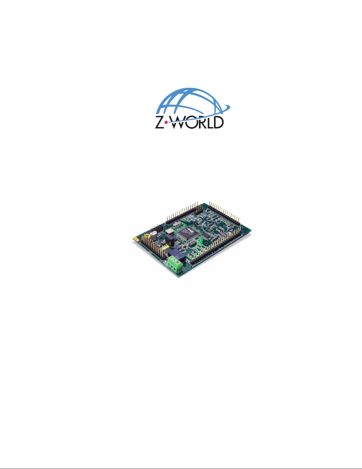
Fox (LP3500)
C-Programmable Single -Board Compu ter
User’s Manual
019–0111 • 041029–E
Page 2

Fox (LP3500) User’s Manual
Part Number 019-0111 • 041029–E • Printed in U.S.A.
©2002–2004 Z-World Inc. • All rights reserved.
Z-World reserves the right to make changes and
improvements to its products without provi ding not ice.
Trademarks
Rabbit and Rabbit 3000 are registered trademarks of Rabbit Semiconductor.
Dynamic C is a registered trademark of Z-W o rld Inc.
Z-World, Inc.
2900 Spafford Street
Davis, California 95616-6800
USA
Telephone: (530) 757-3737
Fax: (530) 753-5141
www.zworl d.com
Fox (LP3500)
Page 3

TABLE OF CONTENTS
Chapter 1. Introduction 1
1.1 LP3500 Description..............................................................................................................................1
1.2 LP3500 Features...................................................................................................................................2
1.3 Optional Add-Ons.................................................................................................................................3
1.4 Development and Evaluation Tools......................................................................................................4
1.4.1 Tool Kit.........................................................................................................................................4
1.4.2 Software........................................................................................................................................5
1.5 CE Compliance.....................................................................................................................................6
1.5.1 Design Guidelines.........................................................................................................................7
1.5.2 Interfacing the LP3500 to Other Devices .....................................................................................7
Chapter 2. Getting Started 9
2.1 LP3500 Connections.............................................................................................................................9
2.2 Remove Battery Tab...........................................................................................................................13
2.3 Installing Dynamic C..........................................................................................................................14
2.4 Starting Dynamic C ............................................................................................................................14
2.5 PONG.C..............................................................................................................................................15
2.6 Where Do I Go From Here? ...............................................................................................................15
Chapter 3. Subsystems 17
3.1 LP3500 Pinouts...................................................................................................................................18
3.1.1 Headers and Screw Terminals.....................................................................................................18
3.2 Power Modes ......................................................................................................................................19
3.2.1 Setting the Power-Save Mode.....................................................................................................20
3.2.2 Operating in the Power-Save Mode............................................................................................21
3.2.3 Resuming Normal-Power or Low-Power Operation ..................................................................21
3.3 Digital I/O...........................................................................................................................................22
3.3.1 Digital Inputs...............................................................................................................................22
3.3.2 Digital Outputs............................................................................................................................23
3.4 Serial Communication ........................................................................................................................25
3.4.1 RS-232 ........................................................................................................................................26
3.4.2 RS-485 ........................................................................................................................................26
3.4.3 Serial Interface Port ....................................................................................................................28
3.4.4 Programming Port.......................................................................................................................28
3.5 Display Interface.................................................................................................................................29
3.6 A/D Converter Inputs (LP3500 only) .................................................................................................30
3.7 PWM Outputs.....................................................................................................................................32
3.8 Relay Output Circuit (LP3500 only) ..................................................................................................33
3.9 Memory...............................................................................................................................................34
3.9.1 SRAM .........................................................................................................................................34
3.9.2 Flash Memory.............................................................................................................................34
Chapter 4. Software 35
4.1 Upgrading Dynamic C........................................................................................................................36
4.1.1 Patches and Bug Fixes................................................................................................................36
4.1.2 Upgrades .....................................................................................................................................36
User’s Manual
Page 4

4.2 Programming Cable............................................................................................................................37
4.2.1 Switching Between Program Mode and Run Mode...................................................................37
4.2.2 Detailed Instructions: Changing from Program Mode to Run Mode.........................................37
4.2.3 Detailed Instructions: Changing from Run Mode to Program Mode.........................................37
4.3 Sample Programs................................................................................................................................38
4.3.1 Power Modes..............................................................................................................................38
4.3.2 Digital I/O...................................................................................................................................38
4.3.3 Serial Communication................................................................................................................ 39
4.3.4 A/D Converter Inputs.................................................................................................................39
4.3.5 PWM Outputs............................................................................................................................. 40
4.3.6 Relay Output...............................................................................................................................40
4.3.7 Vcc Monitoring .......................................................................................................................... 40
4.3.8 LP3500 Calibration .................................................................................................................... 40
4.3.9 LCD/Keypad Module Sample Programs....................................................................................41
4.4 LP3500 Libraries................................................................................................................................42
4.5 LP3500 Function APIs.......................................................................................................................43
4.5.1 LP3500 Power Modes................................................................................................................43
4.5.2 Board Initialization..................................................................................................................... 47
4.5.3 Digital I/O...................................................................................................................................48
4.5.4 Serial Communication................................................................................................................ 50
4.5.5 A/D Converter Inputs.................................................................................................................52
4.5.6 Vcc Monitoring (LP3500 only)..................................................................................................64
4.5.7 PWM Outputs............................................................................................................................. 65
4.6 Relay Output (LP3500 only) ..............................................................................................................66
Appendix A. LP3500 Specifications 67
A.1 Electrical and Mechanical Characteristics ........................................................................................68
A.1.1 Exclusion Zone..........................................................................................................................71
A.1.2 Headers...................................................................................................................................... 72
A.2 Conformal Coating............................................................................................................................73
A.3 Jumper Configurations......................................................................................................................74
A.4 Use of Rabbit 3000 Parallel Ports..................................................................................................... 77
Appendix B. Prototyping Board 81
B.1 Mechanical Dimensions and Layout................................................................................................. 82
B.2 Using the Prototyping Board............................................................................................................. 83
B.2.1 Interface to LP3500 ................................................................................................................... 83
B.2.2 Demonstration Board................................................................................................................. 84
B.2.3 Prototyping Area........................................................................................................................ 84
Appendix C. LCD/Keypad Module 85
C.1 Specifications.....................................................................................................................................85
C.2 Contrast Adjustment..........................................................................................................................87
C.3 Keypad Labeling................................................................................................................................88
C.4 Header Pinouts...................................................................................................................................89
C.4.1 I/O Address Assignments.......................................................................................................... 89
C.5 Bezel-Mount Installation................................................................................................................... 90
C.6 Connect the LCD/Keypad Module to Your LP3500......................................................................... 92
C.7 LCD/Keypad Module Function APIs................................................................................................ 93
C.7.1 LEDs.......................................................................................................................................... 93
C.7.2 LCD Display..............................................................................................................................94
C.7.3 Keypad.....................................................................................................................................110
C.8 Sample Programs............................................................................................................................. 113
Appendix D. Plastic Enclosure 115
D.1 Assembly Instructions..................................................................................................................... 116
D.2 Dimensions......................................................................................................................................118
Fox (LP3500)
Page 5

Appendix E. Power Management 119
E.1 External Power Supply .....................................................................................................................119
E.2 Batteries and External Battery Connections.....................................................................................121
E.2.1 Replacing the Backup Battery..................................................................................................122
E.2.2 Power to VRAM Switch...........................................................................................................122
E.2.3 Reset Generator........................................................................................................................123
E.3 Chip Select Circuit ...........................................................................................................................123
Appendix F. Programming Cable 125
Appendix G. Running a Sample Program 129
Notice to Users 131
Index 133
Schematics 137
User’s Manual
Page 6

Fox (LP3500)
Page 7

1. INTRODUCTION
The LP3500 is a low-po we r sin gle -bo ard computer with built- i n
analog and digital I/O. Although the LP3500 was designed specifically for low-power applications and data logging, it has a
host of features that make it attractive for other applicat ions as
well. Low power is often required in portable equipment operating from batteries or from solar pow er. The LP3500 is ideal for
monitoring equipment o r processes that are far-removed from a
power supply, remote telemetry (RTUs), pipeline control and
monitoring, well-head monitoring; and use on mobile equipment
such as refrigeration trucks.
An optional plasti c enclosure a nd an
LCD/keypad module are available.
The Tool Kit has the essentials that you need to design your own
low-power microprocessor-based system, and includes a complete Dynamic C software development system.
1.1 LP3500 Description
The LP3500 is a low-power single-board computer that incorporates the powerful and
low-EMI Rabbit 3000 microprocessor, flash memory, static RAM, digital I/O ports, A/D
converter inputs, PWM outputs, RS-232/RS-485 serial ports, and both parallel and serial
interfaces that allow other devices to be connected to the LP3500.
All aspects of the LP3500 are designed for low power consumption and operates at a variety of power levels, including a power-save mode, to fit customer-specified conditions at
any given time. The CPU runs at a nominal speed of 7.4 MHz, and operates at 2.8 V to
conserve power. The LP3500 consumes less than 20 mA when fully operational, and less
than 100 µA when in the power-save mode. A replaceable coin-type battery will allow the
LP3500 to operate in sleep mode for over 3 years. The LP3500 is normally powered from
an external battery or power supply. When the unit is in the power-save mode, it can be
awakened by an internal timer, an RS-232 signal, or via polling of an external input. The
LP3500 can be switched from the power-save mode to full operation and back under program control. In addition, various sections of circuitry (such as the RS-232 ports) can be
switched off under program control to further conserve power when not in use.
User’s Manual 1
Page 8
1.2 LP3500 Features
• Rabbit 3000® microprocessor operating at up to 7.4 MHz.
• 512K/128K static RAM and 512K/256K flash memory options.
• 26 digital I/O: 16 protected digital inputs and 10 high-current digital outputs provide
sinking and sourcing outputs.
• 8 single-ended or 4 differential analog channels with Vcc monitoring option : 1 1-bit singleended or 12-bit differential chan nels.
• 3 PWM outputs.
• Six serial ports
1 RS-485
3 RS-232 (one 5-wire and one 3-wire or three 3-wire), jumper option for logic-level
outputs; Serial Port E has a “listen” and “wake-up” capability
1 logic-level serial interface for optional add-ons
1 asynchronous clocked serial port dedicated for programming
• Battery-backed real-time clock.
• Watchdog supervisor.
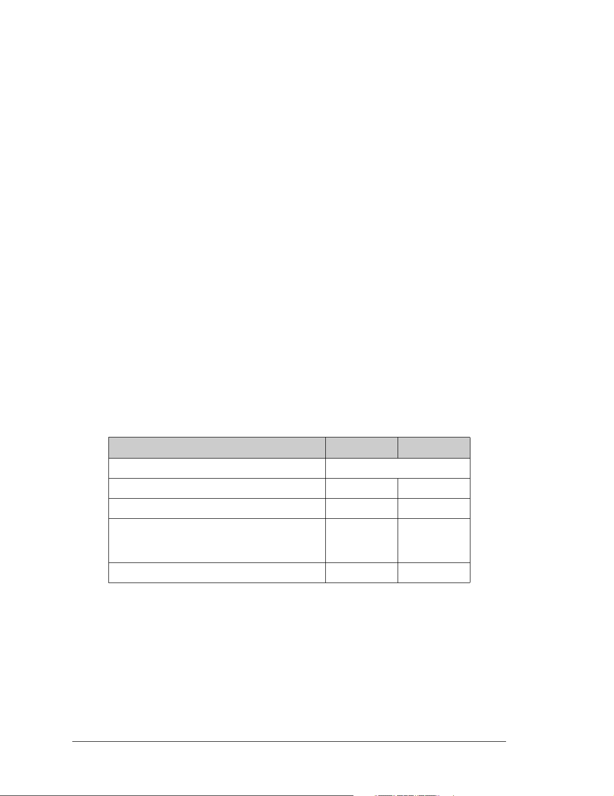
Two LP3500 models are available. Their standard features are summarized in Table 1.
Table 1. LP3500 Models
Feature LP3500 LP3510
Microprocessor Rabbit 3000 running at 7.4 MHz
Static RAM 512K 128K
Flash Memory 512K 256K
A/D Converter Inputs
(ranges from 0–1 V DC to 0–20 V DC, 4 channels
may be individually configured for 4–20 mA)
C-form Bistable Rel a y Yes No
Yes No
Appendix A provides detailed specifications.
The LP3500 can be mounted in two ways. It can be mounted to a panel or on a plastic-
enclosure base, which allows I/O connections to be made using traditional connectors with
0.1" spacing. The LP3500 can also be inverted and mounted directly to mating connectors
on a motherboard of the customer's design. The first approach is appropriate where I/O
connections go directly to devices and switches. The second approach is appropriate
where additional circuitry is incorporated on the motherboard.
2 Fox (LP3500)
Page 9

1.3 Optional Add-Ons
• Plastic enclosure (can be wall-mounted or panel-mounted), which consists of a base
and a cover for either the LP3500 by itself or an assembly made up of the LP3500 and
the LP3500 Prototyping Board. The base is also available separately.
• The Prototyping Board included with the Tool Kit is a convenient means of interfacing
to the LP3500 via the screw-terminal headers on the Prototyping Board. The Prototyping Board is also available for separate purchase.
• 4M and 8M serial flash expansion cards.
• LCD/keypad module with 7-key keypad and seven LEDs.
Further details on the Prototyping Board, the plastic enclosure, and the LCD/keypad module are provided in Appendix B, Appendix C, and Appendix D.
V isi t Z-World’s W e b site for up-to-date information about additional add-ons and features
as they become available. The Web site also has the latest revision of this user’s manual
and schematics.
User’s Manual 3
Page 10
1.4 Development and Evaluation Tools
1.4.1 Tool Kit
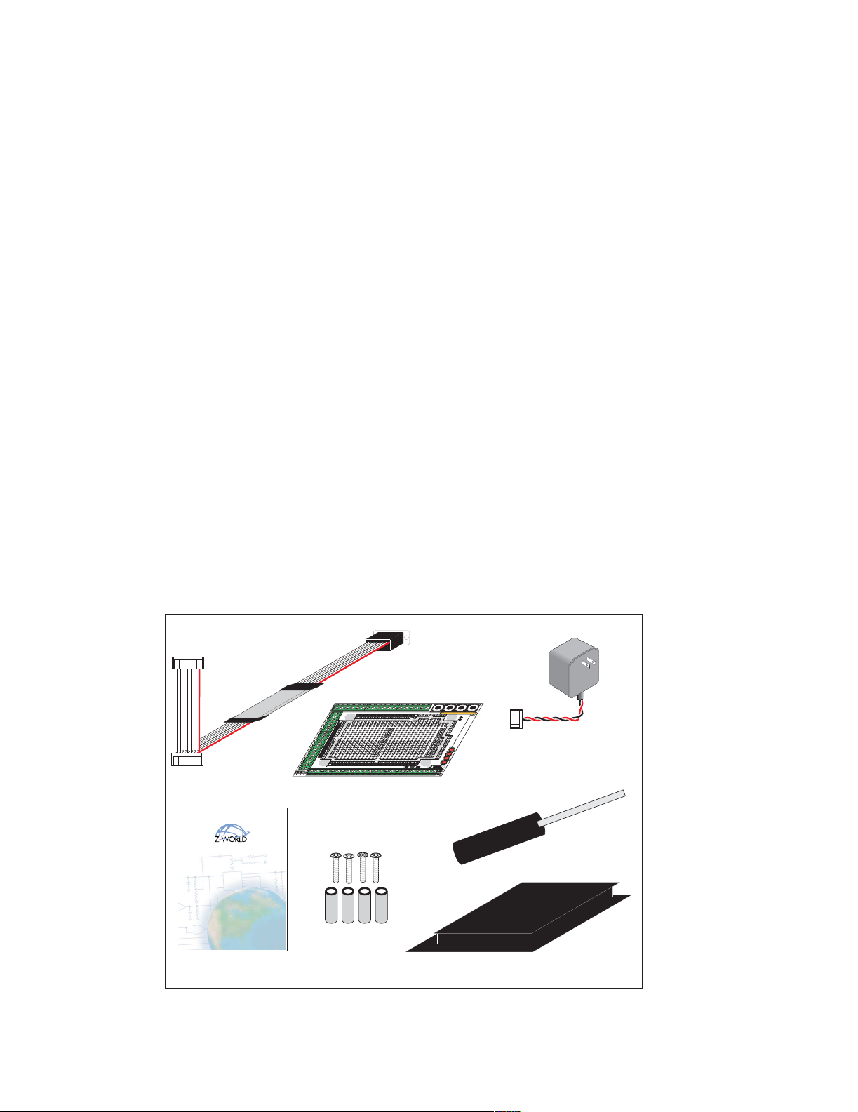
A T ool Kit contains the hardware essentials you will need to develop applications with the
LP3500 single-board computer. The items in the Tool Kit and their use are as follows.
• LP3500 User’s Manual with schematics (this document).
• Dynamic C CD-ROM, with complete product documentation on disk.
• Programming cable, used to connect your PC serial port to the LP3500.
• AC adapter, used to power the LP3500 via the Prototyping Board
. The AC adapter is
supplied with Tool Kits sold in the North American market. If you are using another
power supply, it must provide 3 to 30 V DC
.
• Prototyping Board with pushbutton switches, LEDs, and screw-terminal headers. The
Prototyping Board can be hooked up to the LP3500 to demonstrate the I/O capabilities
of the LP3500 and to provide a prototyping area for you to develop your own add-on
circuits. The screw-terminal headers extend the LP3500’ s headers for development, and
can also be used in a production environment.
• Plastic enclosure with four screws.
• Four stand-offs with mounting screws.
• Screwdriver.
• Rabbit 3000 Processor Easy Reference poster.
• Registration card.
Programming
DIAG
PROG
Cable
(101-0276)
J23
I
N
1
5
I
N
1
J
4
1
1
I
N
1
3
I
N
1
2
I
N
1
1
I
N
1
0
I
N
0
9
I
N
0
8
G
V
N
I
N
D
G
N
J
D
1
2
I
N
0
7
I
N
0
6
I
N
0
5
I
N
0
4
I
N
0
3
J
I
N
1
0
2
I
N
0
1
J
1
3
I
N
0
0
J41
G
N
D
J3
3 V VBAT
GND RxE TxE GND RxC TxC GND RxB TxB GND + 485 GND +K OUT9 OUT8 OUT7 OUT6 OUT5 OUT4 OUT3 OUT2 OUT1 OUT0
J4
J42
J21
J22
J2
VIN
GND
GND
VIN
R1
J44
J43
GND VIN GND VBAT EXT GND PWM2 PWM1 PWM0 GND AIN7 AIN6 AIN5 AIN4 AIN3 AIN2 AIN1 AIN0 GND
S4
VIN
GND
G
V
N
I
N
D
G
V
N
I
N
D
S
D
2
S
D
3
S
D
4
S
D
D1
R
W
P
J5
AC Adapter
(North American
kits only)
S1
S2
S3
RN1
1
Screwdriver
Prototyping Board
Fox (LP3500)
C-Programmable Single-Board Computer
Users Manual
0190111 020815A
Stand-Offs
User's Manual
and Screws
Plastic Enclosure
Figure 1. Tool KitLP3500 Tool KitTool Kit
4 Fox (LP3500)
Page 11

1.4.2 Software
The LP3500 is programmed using version 7.26P or later of Z-World’s Dynamic C. A com-
patible version is inclu ded on t he Tool Kit CD-ROM.
Library functions provide an easy-to-use
interface for the LP3500. Software drivers for digital and analog I/O, and for serial communication are included with Dynamic C. Web-based technical support is included at no
extra charge.
Z-World also offers add-on Dynamic C modules containing the popular µC/OS-II realtime operating system, as well as PPP, Advanced Encryption Standard (AES), and other
select libraries. In addition to the Web-based technical support included at no extra charge,
a one-year telephone-based technical support module is also available for purchase. Visit
our Web site at www.zworld.com
or contact your Z-World sales representative or autho-
rized distributor for further information.
User’s Manual 5
Page 12
1.5 CE Compliance
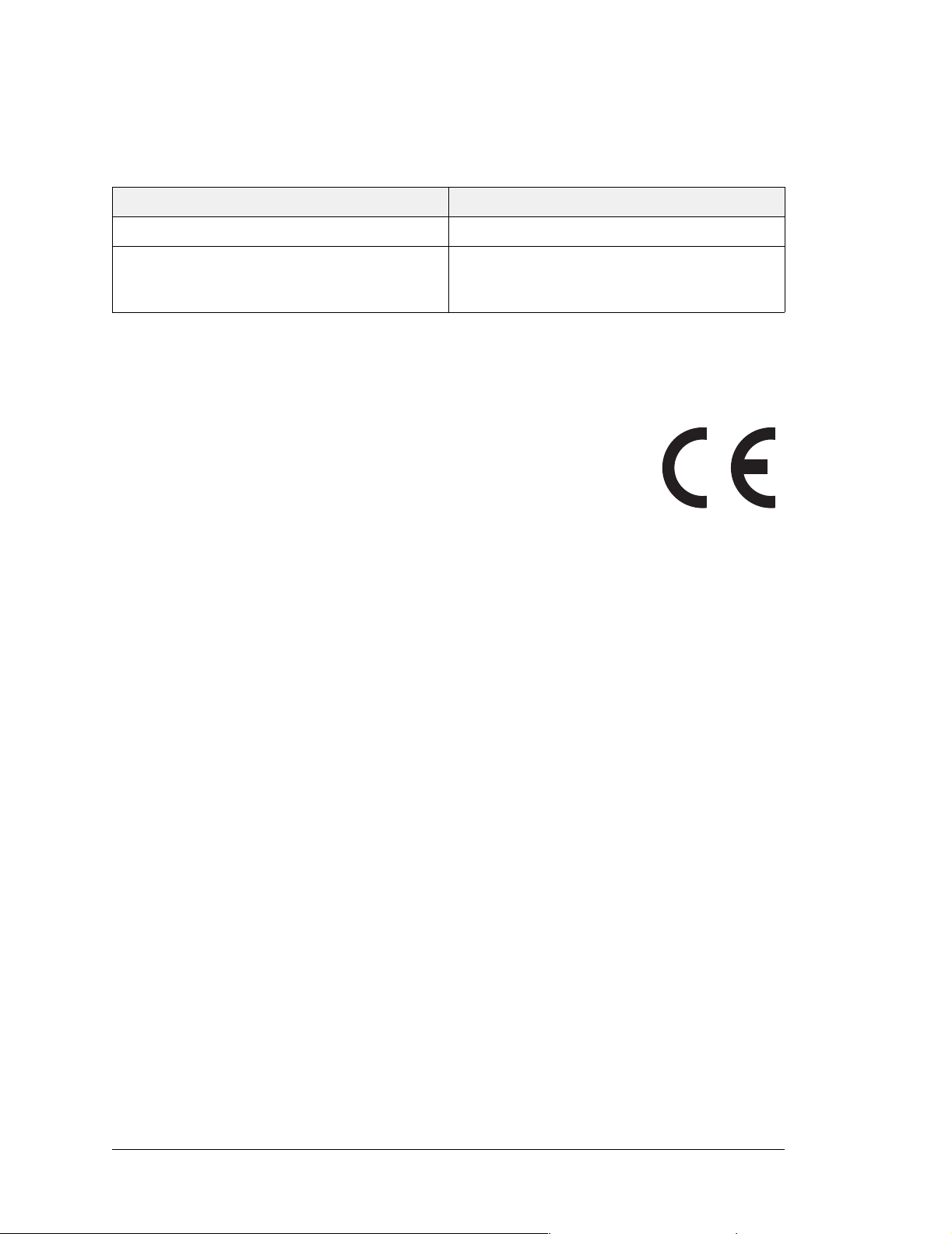
Equipment is generally divided into two classes.
CLASS A CLASS B
Digital equipment meant for light industrial use Digital equipment meant for home use
Less restrictive emissions requirement:
less than 40 dB µV/m at 10 m
(40 dB relative to 1 µV/m) or 300 µV/m
More restrictive emissions requirement:
30 dB µV/m at 10 m or 100 µV/m
These limits apply over the range of 30–230 MHz. The limits are 7 dB higher for frequencies
above 230 MHz. Although the test range goes to 1 GHz, the emissions from Rabbit-based
systems at frequencies above 300 MHz are generally well below background noise levels.
The LP3500 has been tested and was found to be in conformity with the
following applicable immunity and emission standards. The LP3510 is
also CE qualified as it is a sub-version of the LP3500. Boards that are
CE-compliant have the CE mark.
NOTE: Earlier versions of the LP3500 sold before 2003 that do not
have the CE mark are not CE-complaint.
Immunity
The LP3500 series of single-board computers meets the following EN55024/1998 immunity standards.
• EN61000-4-3 (Radiated Immunity)
• EN61000-4-4 (EFT)
• EN61000-4-6 (Conducted Immunity)
Additional shielding or filtering may be required for a heavy industrial environment.
Emissions
The LP3500 series of single-board computers meets the following emission standards
emission standards with the Rabbit 3000 spectrum spreader turned on and set to the normal mode.
• EN55022:1998 Class B
• FCC Part 15 Class B
Your results may vary, depending on your application, so additional shielding or filtering
may be needed to maintain the Class B emission qualification.
6 Fox (LP3500)
Page 13

1.5.1 Design Guidelines
Note the following requirements for incorporating the LP3500 series of single-board
computers into your application to comply with CE requirements.
General
• The power supply provided with the Tool Kit is for development purposes only . It is the
customer’s responsibility to provide a CE-compliant power supply for the end-product
application.
• When connecting the LP3500 to outdoor cables, the customer is responsible for provid-
ing CE-approved surge/lightning protection.
• Z-World recommends placing digital I/O or analog cables that are 3 m or longer in a
metal conduit to assist in maintaining CE compliance and to conform to good cable
design practices. Z-W orld also recommends using properly shielded I/O cables in noisy
electromagnetic environments.
Safety
• For personal safety, all inputs and outputs to and from the LP3500 must not be con-
nected to voltages exceeding SELV levels (42.4 V AC peak, or 60 V DC). Damage to
the Rabbit 3000 microprocessor may result if voltages outside the design range of 0 V
to 40 V DC are applied directly to any of its digital inputs.
• The lithium backup battery circuit on the LP3500 has been designed to protect the bat-
tery from hazardous conditions such as reverse charging and excessive current flows.
Do not disable the safety features of the design.
1.5.2 Interfacing the LP3500 to Other Devices
There are two versions of the LCD/keypad module that may be used with the LP3500:
without a bezel (Z-World part number 101-0601), and a remote panel-mounted version
with bezel (Z-World part number 101-0541). The cable used to connect the LCD/keypad
module should be less than 30 cm (12") to maintain CE compliance. Appendix C provides
complete information for mounting and using the LCD/keypad module.
Since the LP3500 series of single-board computers is designed to be connected to other
devices, good EMC practices should be followed to ensure compliance. CE compliance is
ultimately the responsibility of the integrator. Additional information, tips, and technical
assistance are available from your authorized Z-World distributor, and are also available
on our Web site at www.zworld.com
.
User’s Manual 7
Page 14

8 Fox (LP3500)
Page 15
2. GETTING S TARTED
Chapter 2 explains how to connect the programming cable and
power supply to the LP3500.
2.1 LP3500 Connections
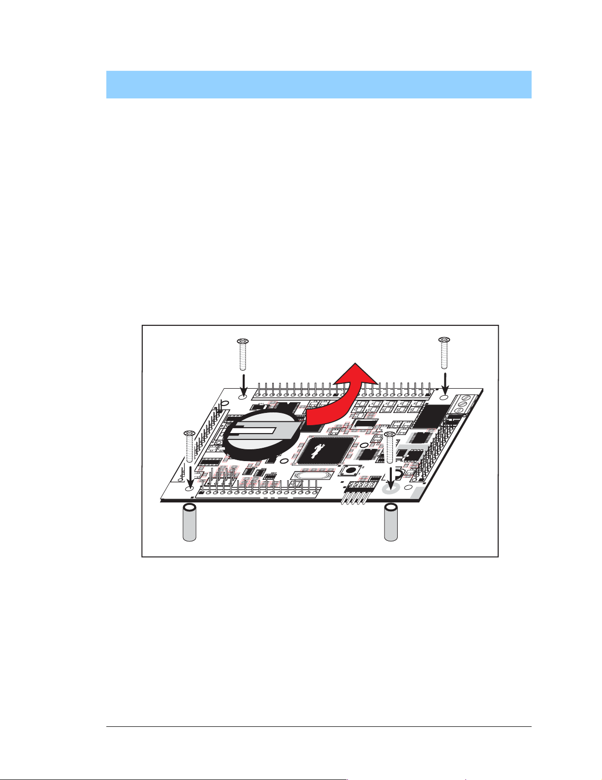
1. Use the 4-40 screws supplied with the Tool Kit to attach the metal stand-offs to your
LP3500 series board as shown in Figure 2.
O
O
O
O
O
U
U
U
U
U
T
T
3
D
3
0
Q16
D33Q14
U
1
R
3
5
1
Q20
R54
GND
GND
T
T
T
1
0
2
D
3
4
Q17
K1
D32
C67
U12
C
7
0
R58
J8
RELAY
C
N
M
O
C
O
N
R
5
6
R
5
5
J9
Y
A
L
P
IS
D
J1
IN
0
0
IN
RN2
0
1
IN
0
2
IN
0
3
IN
0
4
IN
0
5
IN
0
6
IN
0
7
G
N
D
IN
0
8
IN
0
9
IN
1
0
IN
1
1
IN
1
2
IN
1
3
IN
1
4
IN
1
D1
5
C
D4
D2
6
C
D8
8
C10 C13
C
RN1
2
R13
C
3
R6
R16
R
R7
1
7
R9
R1
AIN0 AIN1 AIN2 AIN3
AIN0 AIN1 AIN2 AIN3 AIN4 AIN5 AIN6 AIN7 GND GND
J3
O
O
O
O
O
U
U
J4
U1
R
P
Battery
1
7
BT1
C
4
4
Y1
C
4
0
P
VBAT
EXT
7
R
3
1
C36
R
5
C
4
3
GND VIN GND
D
1
9
D21
D18
C48
R
3
4
U3
U8
R40 C54
R36
C50
D22
J2
C16
C19
D
1
C
5
1
5
D
C
1
7
1
2
C20
C22
D5
D
1
1
D7
4
R
1
8
R20
R22
C
2
9
D13
R
2
3
Q22
R30
C
2
C26
C33
R
R32
R25
2
9
C
R26
3
7
P
P
W
W
W
M
M
M
1
2
0
+K GND 485 + GND TxB RxB GND TxC RxC GND TxE RxE GND
9
D
R
2
3
0
7
D25
Q
5
R
4
2
R
3
Q6
8
C
5
3
C51
R
R
4
3
R44
C55
1
9
C
5
9
C
6
0
U9
S1
RESET
R50
R49
J5
PROGRAM
PORT
U
U
U
T
T
T
T
T
8
5
4
7
6
D
D
2
2
8
6
Q
8
Q10
R43
R33
Q13
Y2
C
6
1
Q12
R47
R
4
5
U11
J6
6
6
C
R48
U10
C
6
RP13
4
C65
R
P
1
4
Figure 2. Attach Stand-Of fs and Remove Battery Cap
2. Remove the battery cap from the coin-type lithium-ion battery installed on the LP3500
series board. The battery cap was inserted in the factory to keep the battery fresh until
you are ready to use the board.
User’s Manual 9
Page 16
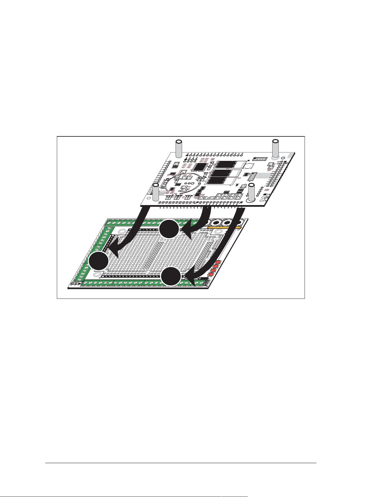
3. Attach the LP3500 main board to the Prototyping Board as shown in Figure 3.
Press the headers on the LP3500 series board firmly into the corresponding header sock-
ets located at J1, J2, and J4 on the Prototyping Board.
NOTE: It is important that you line up the header pins on the LP3500 exactly with the
corresponding
pins may become bent or damaged if the pin alignment is offset, and the LP3500 will
not work. Permanent electrical damage may also result if a misaligned LP3500 is
powered up.
header sockets J1, J2, and J4 on the Prototyping Board. The header
PORT
PROGRAM
/RESET
TP2
RESET
S2
Q21
C
6
3
Q19
Q18
R53
R52
C
C
6
6
9
8
LP3500
R27
C38
R21
R
R28
R19
2
D3
R8
R5
C9
C14
RP1
D9
C
7
RP2
C
5
C17
C4
C1
D6
D10
J
P
1
2
RP4
RP3
D16
VCC
R4
R12
GND
R3
+K
R2
IN
J
P
1
D14
R11
J
J
P
R10
P
C
C25
5
3
07
815
1
8
J
P
4
J
C
P
3
2
1
4
C27
C34
J
R15
P
1
0
C
R14
C23
D12
C30
C28
J
P
6
4
1
J
P
9
C
4
2
U2
J
P
8
J
J
P
P
7
1
1
R
P
9
R
P
8
R
C
5
4
9
9
R35
RP10
Q7
Q
D23
Q4
9
Q3
D27
D24
U7
U6
R46
RP11
RP12
Q11
Q15
D29
D31
I
N
1
5
I
N
1
4
I
N
1
3
I
N
1
2
I
N
1
1
I
N
1
0
I
N
0
9
I
N
0
8
G
N
J
D
1
2
I
N
0
7
I
N
0
6
I
N
0
5
J1
I
N
0
4
I
N
0
3
J
I
N
1
0
2
I
N
0
1
J
1
I
3
N
0
0
N
D
3 V VBAT
G
J41
J3
GND RxE TxE GND RxC TxC GND RxB TxB GND + 485 GND +K OUT9 OUT8 OUT7 OUT6 OUT5 OUT4 OUT3 OUT2 OUT1 OUT0
J23
J
1
1
G
V
N
I
N
D
J42
J22
GND
VIN
J4
Figure 3. Attach LP3500 Main Board to Prototyping Board
GND VIN GND VBAT EXT GND PWM2 PWM1 PWM0 GND AIN7 AIN6 AIN5 AIN4 AIN3 AIN2 AIN1 AIN0 GND
J2
J4
J21
VIN
GND
VIN
GND
R1
D1
J44
J5
J2
J43
S3
S4
G
V
N
I
N
D
G
V
N
I
N
D
1
S
D
2
S
D
3
S
D
4
S
D
R
W
P
S1
S2
RN1
Prototyping
Board
10 Fox (LP3500)
Page 17
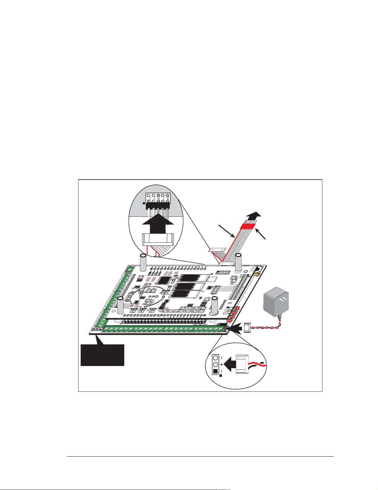
4. Connect the programming cable to download programs from your PC and to program
and debug the LP3500.
NOTE: Use only the programming cable that has a red shrink wrap around the RS-232
level converter (Z-World part number 101-0276), which is supplied with the LP3500
Tool Kit. Other Z-World programming cables might not be voltage-compatible or their
connector sizes may be different.
Connect the 10-pin PROG connector of the programming cable to header J5 on the LP3500
board. Ensure that the colored edge lines up with pin 1 as shown. There is a small dot on the
circuit board next to pin 1 of header J5. (Do not use the
DIAG connector, which is used for
monitoring only, as explained in Appendix F, “Programming Cable.”) Connect the other
end of the programming cable to a COM port on your PC. Make a note of the port to
which you connect the cable, as Dynamic C will need to have this parameter configured.
Note that COM1 on the PC is the default COM port used by Dynamic C.
1
2
I
N
1
1
I
N
1
0
I
N
0
9
IN
0
8
G
N
D
I
N
0
7
I
N
0
6
I
N
0
5
I
N
0
4
I
N
0
3
J
I
N
1
0
2
I
N
0
1
J
1
I
3
N
0
0
G
N
D
3 V VBAT
J41
J3
GND RxE TxE GND RxC TxC GND RxB TxB GND + 485 GND +K OUT9 OUT8 OUT7 OUT6 OUT5 OUT4 OUT3 OUT2 OUT1 OUT0
X
Do not connect
AC adapter to
VBAT terminal
J5
PROGRAM
PORT
PC COM port
Colored edge
PROG
DIAG
PROG
GND VIN GND VBAT EXT GND PWM2 PWM1 PWM0 GND AIN7 AIN6 AIN5 AIN4 AIN3 AIN2 AIN1 AIN0 GND
S4
PORT
R27
C38
R21
R
R28
I
N
1
5
I
N
1
4
I
N
1
3
I
N
J
1
2
J23
D3
J
1
1
C9
RP1
C
7
RP2
C
5
C4
C1
J
P
1
2
G
V
N
I
RP4
N
D
RP3
D16
VCC
R4
R12
GND
R3
R11
J
+K
R2
R10
P
C
3
07
815
IN
1
8
J
J
P
P
4
1
J
P
2
R19
J22
2
4
J2
C27
C34
J
R15
R8
R5
R14
C14
D9
C17
D6
D12
D10
D14
J
P
C25
5
6
C
3
1
J42
P
1
0
C
4
J
1
P
9
C
4
2
U2
C23
J
P
8
J
J
P
P
7
1
1
C30
R
P
9
C28
R
P
8
R
C
5
4
J
9
9
P
R35
GND
VIN
J4
RP10
Q
D23
Q4
9
Q3
D24Q7D27
R1
J43
U7
J21
VIN
GND
U6
R46
RP12
Q11
Q15
D29
D31
J44
PROGRAM
/RESET
TP2
RESET
VIN
Q19
GND
S2
RP11
R53
R52
G
N
D
Q21
C
C
6
6
9
8
G
V
N
I
N
D
D
D1
R
W
P
J5
To
Programming
Cable
Red
shrink wrap
S1
S2
S3
C
6
3
RN1
Q18
V
I
N
1
S
D
2
S
D
3
S
D
4
S
J5
Figure 4. Programming Cable and Power Supply Connections
User’s Manual 11
Page 18
5. Connect the power supply.
Hook up the connector from the wall transformer to header J5 on the Prototyping Board as
shown in Figure 4. The orientation of this connector is not important since the VIN (positive) voltage is the middle pin, and GND is available on both ends of the three-pin header
J5.
NOTE: Do not connect the AC adapter to the VBAT terminal on the Prototyping Board.
The VBAT terminal supplies th e backu p batt ery vo ltage of 3 V, and the LP3500 may b e
damaged if subjected to the raw DC voltage from the AC adapter through the VBAT
terminal.
6. Apply power.
Plug in the AC adapter. If you are using your own power supply, it must provide 3 V to
30 V DC—voltages outside this range could damage the LP3500.
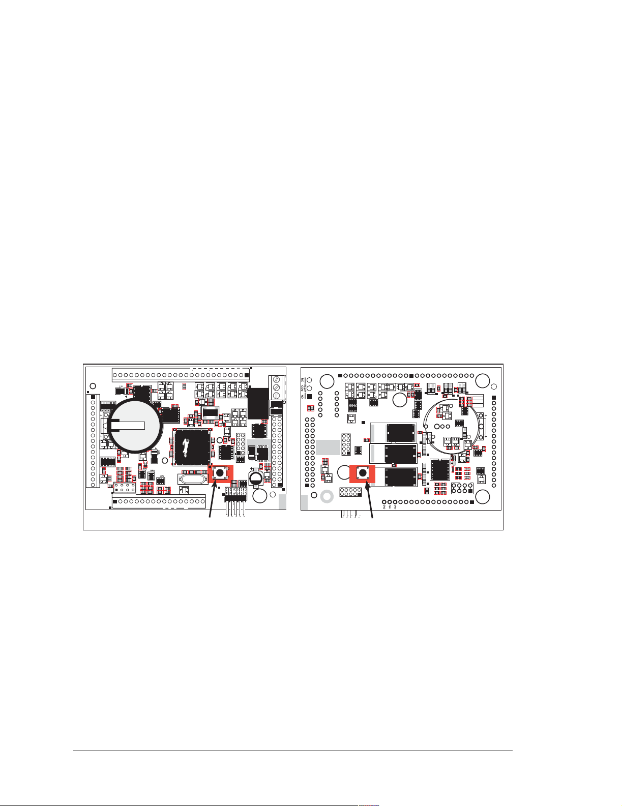
NOTE: A hardware reset may be done by pressing the RESET switch on the LP3500.
The LP3500 may also be reset by unplugging the AC adapter, then plugging it back in.
However, when the LP3500 is operating in the power-save mode, the backup battery
will provide su ffic ient voltage to prev ent a r eset from happening, in which cas e you wil l
have to press the RESET switch on the LP3500.
OUT1
J4
J1
IN00 IN01 IN02 IN03 IN04 IN05 IN06 IN07 GND IN08 IN09 IN10 IN11 IN12 IN13 IN14 IN15
RN2
D5
D7
C6
D4
D2
C8
D8
C10 C13
C2
RN1
C3
R6
R17
R7
R9
D1
R1
AIN0 AIN1 AIN2 AIN3
AIN0 AIN1 AIN2 AIN3 AIN4 AIN5 AIN6 AIN7 GND GND
OUT9
OUT8
OUT7
OUT6
+K GND 485 + GND TxB RxB GND TxC RxC GND TxE RxE GND
D19
C36
RP17
R57
Battery
R31
C29
BT1
C33
R29
R25
C37
R26
D20
D21
D18
C48
U3
C43
C44
Y1
R32
C40
PWM1
PWM0
C16
U1
C19
D15 D17
C15
C12
C20
C22
D11
D13
R23
Q22
R30
C24
R13
R16
R18
C26
R20
J3
R22
D26
R37
D25
Q8
Q5
R42
R38
Q6
C53
C51
R34
R41
R39
R44
C55
U8
R40 C54
R36
C50
D22
VBAT
EXT
GND VIN GND
J2
PWM2
RESET switch
OUT0
OUT2
OUT5
OUT4
OUT3
GND
J8
RELAY
D30
D28
D34
Q17
Q16
Q10
R43
K1
R33
Q13
D32
Y2
C61
Q12
U12
R47
R45
D33Q14
U11
J6
C66
C59
R48
C60
U9
RESET
C64
U13
U10
RP13
S1
C65
R50
R49
RP14
J5
PROGRAM
PORT
NC
COM
NO
R56
R55
C69
C67
J9
C70
R51
R58
Q20
R54
D6
D4
D2
D0
A1
A3
GND
DISPLAY
DPRST
VDISP
GND
GND
OUT0
OUT1
OUT2
OUT3
OUT4
OUT5
D31
D29
PORT
Q9
Q11
TP1
U5
VRAM
R46
RP15
U6
S2
RESET
RESET
U7
U7
TP2
TP2
/RESET
/RESET
Q15
RP12
RP11
C68
D7
Q21
D5
D3
J6
D1
A0
A2
GND
GND
R52
R53
Q18
Q19
DISP
C63
PROGRAM
PORT
PROGRAM
OUT6
D24Q7D27
RP10
OUT7
OUT8
D23
VIN
GND
GND +KGND RxE TxE GND RxC TxC GND RxB TxB GND + 485
OUT9
Q3
Q4
C49
R59
C52
VBAT
EXT
GND
GND
PWM2
R35
C39
C42
C41
R28
PWM1
CTS RTS
C31
JP2
JP1
JP4
IN
815
U4
JP6
JP5
RP8
C28
RP9
JP11
JP7
JP8
U2
JP9
JP10
C34
R24
C38
R27
GND
AIN7
PWM0
07
C25
C18
R10
JP3
R11
D14
R12
D16
RP3
C30
RP4
JP12
D10
D12
D6
C23
C17
C71
IN DR OUT
D9
JP13
C21
C14
R14
R60
R15
420 mA
C27
R19
R21
AIN3
AIN2
AIN6
AIN5
AIN4
AIN3
AIN2
IN00
R2
+K
R3
GND
IN01
R4
VCC
IN02
IN03
IN04
IN05
IN06
IN07
GND
C1
C4
IN08
IN09
C5
IN10
RP2
C7
IN11
RP1
IN12
C9
R5
IN13
R8
IN14
D3
IN15
AIN1
AIN0
AIN1
AIN0
RESET switch
Figure 5. Locations of LP3500 RESET Switches
Reset switches are located on both sides of the LP3500 board.
12 Fox (LP3500)
Page 19
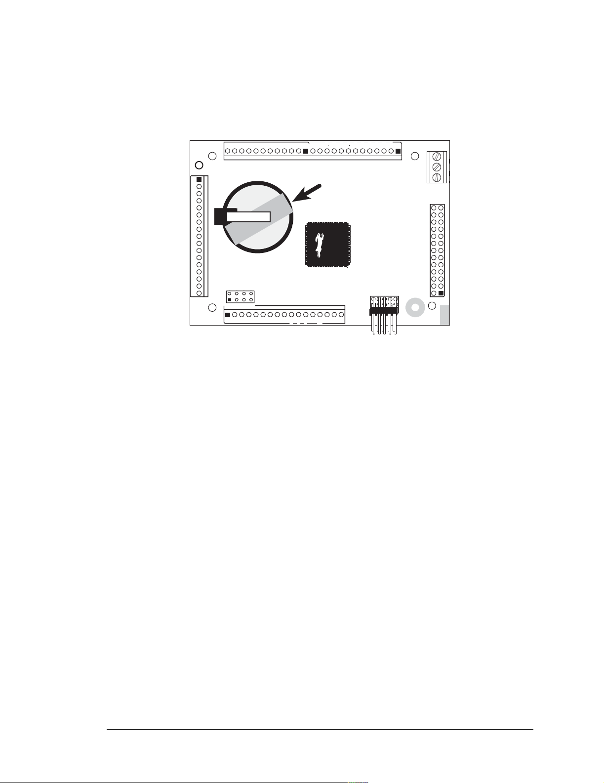
2.2 Remove Battery Tab
The backup battery on the LP3500 has a plastic tab to protect the battery against discharging before the LP3500 is placed into service.
OUT1
OUT0
OUT2
OUT3
OUT4
GND
NC
COM
NO
IN00 IN01 IN02 IN03 IN04 IN05 IN06 IN07 GND IN08 IN09 IN10 IN11 IN12 IN13 IN14 IN15
OUT9
+K GND 485 + GND TxB RxB GND TxC RxC GND TxE RxE GND
OUT8
OUT7
OUT6
Pull
OUT5
Plastic
Tab
DISPLAY
AIN0 AIN1 AIN2 AIN3
PWM1
PWM2
PWM0
AIN0 AIN1 AIN2 AIN3 AIN4 AIN5 AIN6 AIN7 GND GND
VBAT
EXT
GND VIN GND
Figure 6. Remove Battery Tab
GND
NOTE: Z-World recommends that the battery tab not be removed until you are ready to
place the LP3500 in normal service with regular power connected to header J3.
The backup battery protects the contents of the SRAM and keeps the real-time clock
running when regular power to the LP3500 is interrupted. If you plan to use the real-time
clock functionality in your application, you will need to set the real-time clock once you
remove the plastic tab. Set the real-time clock using the onscreen prompts in the demonstration program. Alternatively, you may set the real-time clock using the SETRTCKB.C
sample program from the Dynamic C SAMPLES\RTCLOCK folder. The RTC_TEST.C
sample program in the Dynamic C
SAMPLES\RTCLOCK folder provides additional exam-
ples of how to read and set the real-time clock.
User’s Manual 13
Page 20

2.3 Installing Dynamic C
If you have not yet installed Dynamic C version 7.26P (or a later version), do so now by
inserting the Dynamic C CD in your PC’s CD-ROM drive. The CD will auto-install unless
you have disabled auto-install on your PC.
If the CD does not auto-install, click
Start > Run from the Windows Start button and
browse for the Dynamic C setup.exe file on your CD drive. Click OK to begin the
installation once you have selected the
setup.exe file.
The Dynamic C User’s Manual provides detailed instructions for the installation of
Dynamic C and any future upgrades.
NOTE: If you have an earlier version of Dynamic C already installed, the default instal-
lation of the la te r ver sion wi ll b e in a different folder , and a sep ara te i con wil l app ear on
your desktop.
2.4 St arting Dynamic C
Once the LP3500 is connected to your PC and to a power source, start Dynamic C by double-clicking on the Dynamic C icon or by double-clicking on the
with DcRab in the Dynamic C directory.
Dynamic C assumes, by default, that you are using serial port COM1 on your PC. If you
are
using COM1, then Dynamic C should detect the LP3500 and go through a sequence
steps to cold-boot the LP3500 and to compile the BIOS. If the error message “Rabbit Processor Not Detected” appears, you have probably connected to a different PC serial port
such as COM2, COM3, or COM4. Y ou can change the serial port used by Dynamic C wit h
the OPTIONS menu, then try to get Dynamic C to recognize the LP3500 by selecting
Reset Target/Compile BIOS on the Compile menu. Try the different COM ports in the
OPTIONS menu until you find the one you are connected to. If you still can’t get Dynamic
C to recognize the target on any port, then the hookup may be wrong or the COM port
might not working on your PC.
.exe file associated
of
Dynamic C automatically uses a maximum debug baud rate of 38,400 bps when an
LP3500 series board is in use.
14 Fox (LP3500)
Page 21

2.5 PONG.C
You are now ready to test your set-up by running a sample program.
Find the file
open it with the
PONG.C, which is in the Dynamic C SAMPLES folder. To run the program,
File menu (if it is not still open), compile it using the Compile m enu, and
then run it by selecting Run in the Run menu. The STDIO window will open and will display a small square bouncing around in a box.
This program shows that the CPU is working.
2.6 Where Do I Go From Here?
NOTE: If you purchased your LP3500 through a distributor or Z-World partner, contact
the distributor or Z-World partner first for technical support.
If there are any problems at this point:
• Check the Z-W orld Technical Bulletin Board at www.zworld.com/support/bb/.
• Use the Technical Support e-mail form at www.zworld.com/support/.
If the sample program ran fine, you are now ready to go on to explore other LP3500 features and develop your own applications.
Chapter 3, “Subsystems,” provides a description of the LP3500’s features, Chapter 4,
“Software,” describes the Dynamic C software libraries and introduces some sample programs. These sample programs can be used as templates for applications you may wish to
develop.
User’s Manual 15
Page 22

16 Fox (LP3500)
Page 23
3. SUBSYSTEMS
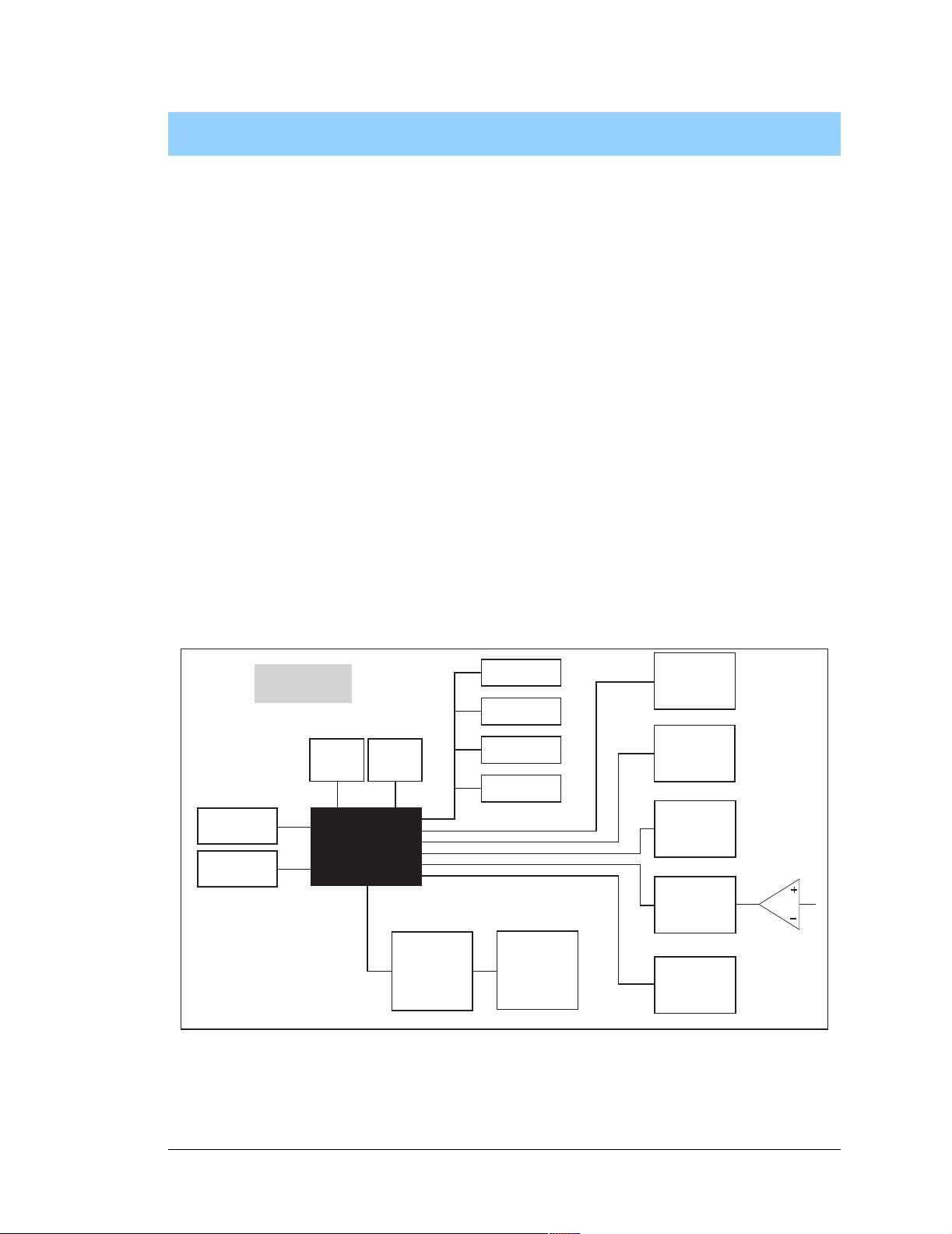
Chapter 3 describes the principal subsystems for the LP3500.
• Power Modes
•Digital I/O
• Serial Communication
• A/D Converter Inputs (LP3500 only)
• PWM Outputs
• Relay Output Circuit (LP3500 only)
• Memory
Figure 7 shows these Rabbit-based subsystems designed into the LP3500.
SRAM
Flash
LP3500
32 kHz
osc
RABBIT
3.7 MHz
3000
Programming
Port
Serial
Interface
RS-232
osc
RS-485
Decoder
Control
Figure 7. LP3500 Subsystems
Interface
to
LCD/Keypad
Module
Digital
Inputs
Digital
Outputs
Relay
Output
A/D
Converter
PWM
Outputs
User’s Manual 17
Page 24
3.1 LP3500 Pinouts
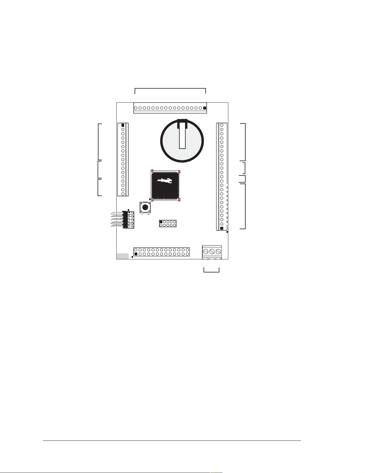
The LP3500 pinouts are shown in Figure 8.
IN15
IN14
IN13
IN12
IN11
IN10
17 16 15 14 13 12 11 10 9 8 7 6 5 4 3 2 1
Analog
Inputs
PWM
Outputs
Power
VBAT EXT
Supply
Programming
Port
AIN0
AIN1
AIN2
AIN3
AIN4
AIN5
AIN6
AIN7
GND
PWM0
PWM1
PWM2
GND
GND
GND
VIN
PROGRAM
PORT
1
2
3
4
5
6
7
8
9
10
11
12
13
14
15
16
17
J5
J2
RESET
S1
Serial
Interface
Digital
Inputs
IN09
IN08
GND
IN07
J6
IN06
IN05
IN04
IN03
IN02
IN01
J4
Battery
IN00
J1
25
GND
24
RxE
23
TxE
22
GND
21
RxC/CTS
TxC/RTS
GND
RxB
TxB
GND
RS-485+
RS-485
GND
+K
OUT9
OUT8
OUT7
OUT6
OUT5
OUT4
OUT3
OUT2
OUT1
OUT0
GND
RS-232
RS-485
K
Digital
Outputs
20
19
18
17
16
15
14
13
12
OUT9
11
OUT8
10
OUT7
9
OUT6
8
OUT5
7
OUT4
6
OUT3
5
OUT2
4
OUT1
3
OUT0
2
1
GND
J8
GND
Display Interface
DISPLAY
J9
NO
J8
RELAY
NC
COM
NC
NO
COM
Relay
Outputs
Figure 8. LP3500 Pinouts
NOTE: Although header J2 is installed on the LP3510, the associated analog I/O are not
available on the LP3510. The relay screw-terminal header at J8 is also not installed on
the LP3510. The power supply inputs on header J2 are still available.
3.1.1 Headers and Screw Terminals
Standard LP3500 models are equipped with two 1 × 17 headers (J1 and J2) with a pitch of
0.1", one 1 × 17 header (J4) with a pitch of 0.1", and one 1 × 3 screw terminal strip (J8).
The Display Interface (J9) is a 2 × 13 header with a pitch of 0.1", and the Serial Interface
is a 2 mm 2 × 5 socket.
A variety of commercially available connectors with a 0.1" pitch can be used to interface
to the signals on headers J1, J2, and J4, or the Prototyping Board may be used to access
these signals via screw-terminal headers.
18 Fox (LP3500)
Page 25
3.2 Power Modes
See note
16 mA
Consumption
Typical Current
Supports
from Table 3
Subsystems
Supports
Relay Output
Power Source
5 mA
1.0 mA
140 µA
140 µA
battery
VIN or external
No No
70 µA
No No 46 µA
lator turned off)
External battery
(with linear regu-
or ext. battery
Onboard ba ttery
See
Code
None VIN Yes Yes
Restrictions
and
SRAM and
Section 3.2.1
Section 3.2.2
R TC updates
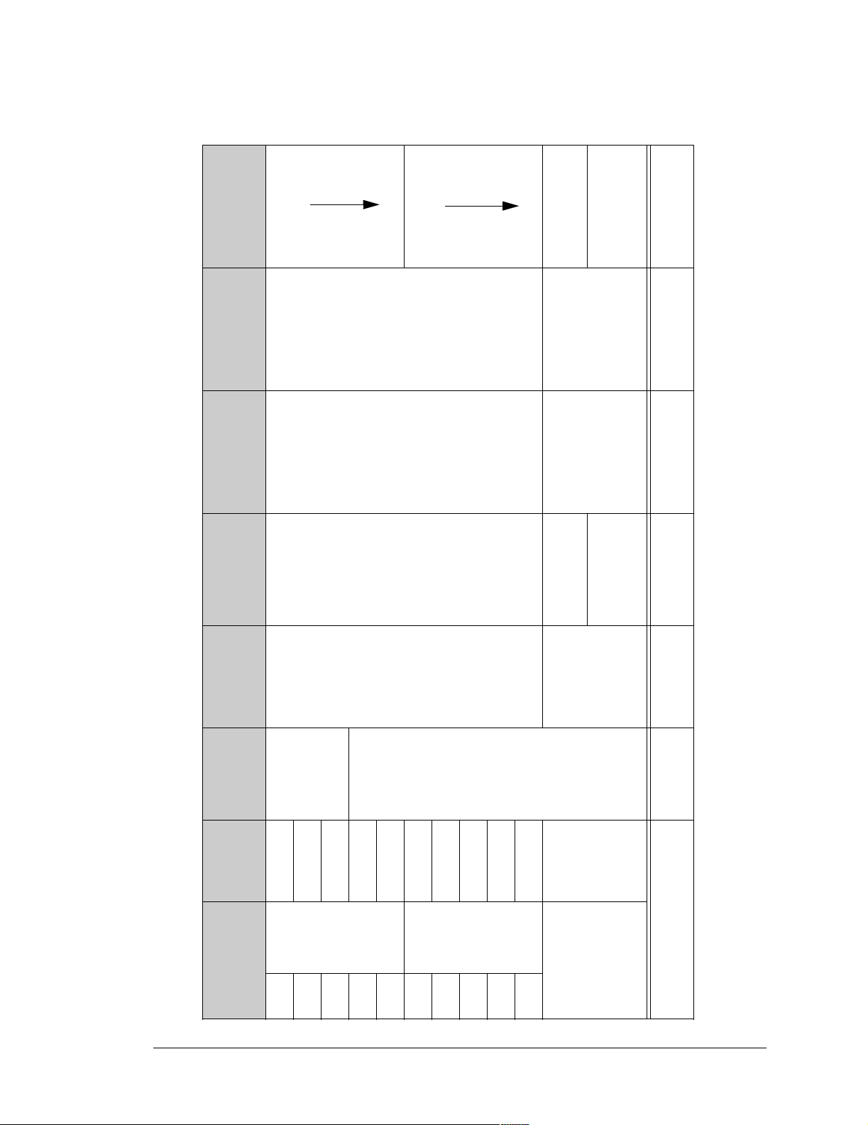
Table 2. Software-Defined Power Modes
Power
8 8.192 kHz
None
Modes
9 4.096 kHz
Processor halted None
10 2.048 kHz
Power-Save Mode 2.048 kHz
NOTE: The actual current consumption depends heavily on the SRAM writes in the user’s program. See Section 3.2.2 for more
information.
Debug
Capability
Clock
Frequency
Mode
User’s Manual 19
Normal
7.3728 MHz
Modes
Normal
2 3.6864 MHz
3 1.8423 MHz
1
4 1.2288 MHz
32.768 kHz
Low-
5 0.9216 MHz
7 16.384 kHz
6
Page 26
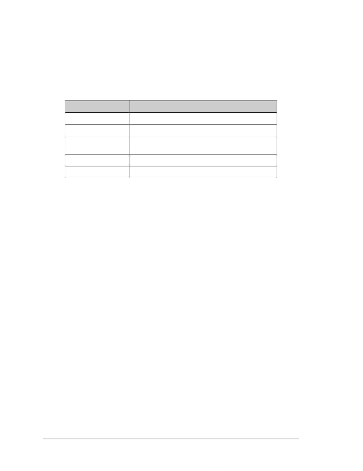
Table 2 lists the power modes based on clock frequency that can be defined in software
using the
powerMode function.
The LP3500 can operate at various power levels, depending on the clock frequency and on
which subsystems on the board are turned off using the
devPowerSet function. Table 3
lists the LP3500 subsystems that can be turned off with the devPowerSet function.
Table 3. LP3500 Subsystems That Can Be Turned Off
LP3500 Section Description
RS-232 Receivers and transmitters are disabled, RxE remains active.
RS-485 Transmitter is disabled.
A/D Converter
(LP3500 model only)
LCD/Keypad Module LCD/keypad module is turned off.
All of the Above All sections are disabled as described above.
NOTE: RxE always remains active when the above systems are turned off to allow the
LP3500 to “listen” while it is in the
ADS7870 internal oscillator is turned off.
power-save mode.
The LP3500 processor turns off automatically when VIN is removed, and the processor
will not operate again until VIN is restored. The onboard battery provides backup for the
SRAM and the real-time clock. VIN must be applied to the LP3500 in order to run or set
the processor in any of the numbered modes listed in Table 2.
3.2.1 Setting the Power-Save Mode
The LP3500 can be placed in the power-save mode using one of three different software
calls,
serCommAlert,
timedAlert, or
digInAlert,
depending on whether you wish to use Serial Port E, a simple timeout, or a digital input to
trigger the LP3500 to resume operation in one of the other power modes.
If you call serCommAlert, then any activity on Serial Port E will trigger the LP3500 out
of the low-power mode. If you call timedAlert, then the LP3500 is triggered out of the
power-save mode when the specified time has elapsed. If you call digInAlert, then the
LP3500 is triggered out of the power-save mode when the specified channel is activated.
In addition, digInAlert and serCommAlert have “backup” timeout parameters associated with them to wake up the LP3500 after a specified period even in the absence of the
digital or serial triggers.
20 Fox (LP3500)
Page 27

3.2.2 Operating in the Power-Save Mode
VIN may be removed to allow the LP3500 to operate using the external battery once the
LP3500 is in Mode 10. At this point, the LP3500 will draw 200 µA after the subsystems
listed in T able 3 are turned off. The LP3500’ s linear regulator may then be turned off using
setpowersource function call, and this will lower the current draw to 100 µA.
the
The LP3500 digital I/O can continue to operate (remember that an independent +K source
is required for the digital outputs) using special software routines.
Here are some tips for when the LP3500 is in the power-save mode.
1. Do not write to the SRAM while the LP3500 is in power-save mode and you are relying
solely on the onboard backup battery.
2. When the linear regulator is turned off, watch your current consumption carefully since
too high a current draw could trigger a system reset and turn off the processor.
3.2.3 Resuming Normal-Power or Low-Power Operation
As long as VIN is still connected and the linear regulator has not been turned off, the
LP3500 will return automatically to the previous power mode once the non-zero timeout
specified in serCommAlert, timedAlert, or digInAlert has elapsed.
NOTE: The processor will tur n o f f if VIN is not ava ilabl e at the e xpirat ion of t he ti meout
or if VIN is not available when a wake-up signal comes in through Serial Port E or the
selected digital input.
When the timeout is set to 0, which corresponds to an indefinite timeout, the LP3500 may
still be restored to a normal power mode from the power-save mode.
1. Make sure that raw DC power is available at VIN.
2. Turn the linear regulator back on using the setpowersource function call.
3. Use the rdPowerState function call to establish that the LP3500 is now operating
from VIN. Note that this function only works with LP3500 models, which have the
A/D converter.
4. Use the powerMode function call to set the desired power mode.
User’s Manual 21
Page 28
3.3 Digital I/O
3.3.1 Digital Inputs
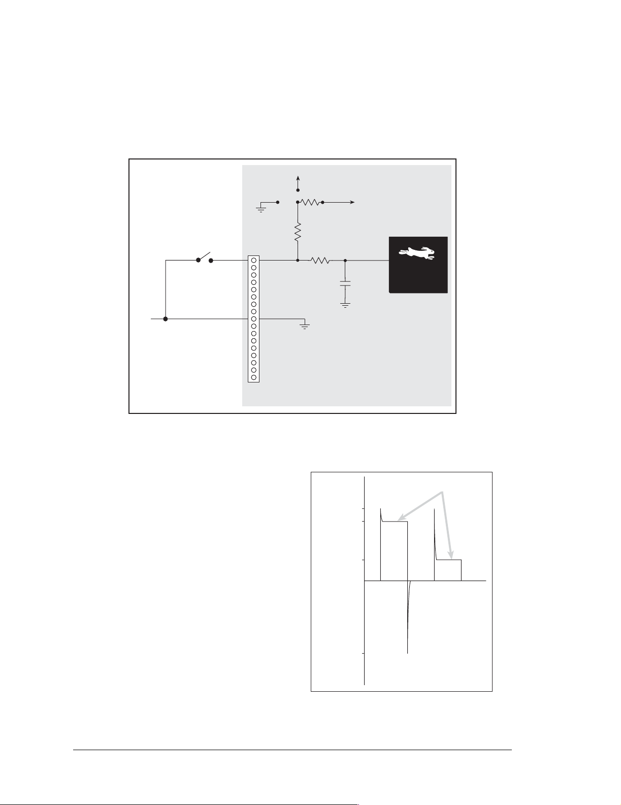
The LP3500 has 16 digital inputs, IN00–IN15. The inputs are factory-configured to be
pulled up to +K in banks of eight, but they can also be pulled up to Vcc or down to 0 V in
banks of eight by changing a surface-mounted 0 Ω resistor as shown in Figure 9.
Vcc
Factory
+K
0 W
22 kW
Default
GND
Figure 9. LP3500 Digital Inputs [Pulled Up—Factory Default]
The digital inputs are each fully protected
over a range of 0 V to +36 V, and can
handle short spikes of ±40 V. The actual
switching threshold is approximately
1.40 V. Anything below this value is a
logic 0, and anything above is a logic 1.
Pulling the digital inputs to Vcc will increase the current consumption by about
300 µA for each digital input.
100 kW
330 nF
+40 V
+36 V
+3.3 V
Microprocessor
Spikes
Rabbit 3000
Normal Switching
Spikes
Levels
Digital Input Voltage
40 V
Figure 10. LP3500 Digital Input Protected
22 Fox (LP3500)
Spikes
Range
Page 29
3.3.2 Digital Outputs
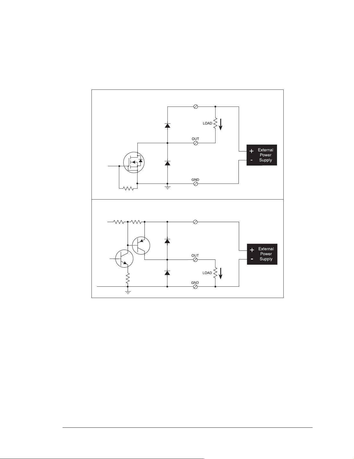
The LP3500 has 10 digital outputs: OUT0–OUT7 can each sink up to 200 mA, and
OUT8–OUT9 can each source up to 200 mA at 36 V. Figure 11 shows a wiring diagram
for using the digital outputs in a sinking or a souring configuration.
SINKING OUTPUTS (OUT0OUT7)
K
Current
Flow
1 MW
SOURCING OUTPUTS (OUT8OUT9)
Vcc
K
Current
Flow
Figure 11. LP3500 Digital Outputs
TIP: Turn the outputs off (high for sourcing outputs and low for sinking outputs) to
reduce current consumption.
User’s Manual 23
Page 30
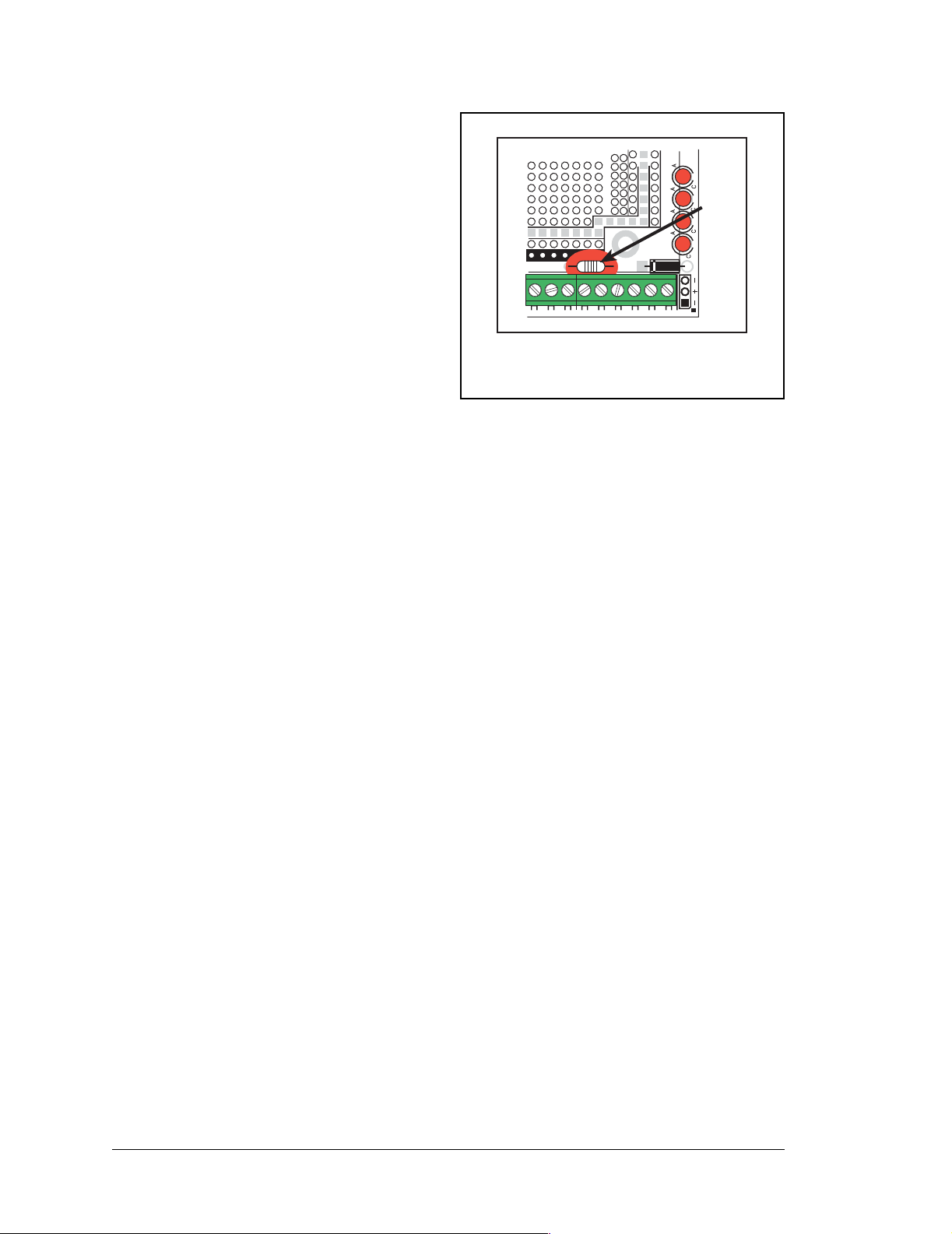
When the LP3500 is connected to the Prototyping Board, a 0 Ω resistor on the Prototyp-
GND
VIN
ing Board (R1) ties +K to VIN, the raw DC
input voltage. Figure 12 shows the location
D1
J5
R1
DS4 DS3 DS2 DS1
PWR
of this 0 Ω resistor on the Prototyping Board.
NOTE: R1 on the Prototyping Broad
must be removed to avoid damage to
the power supplies if you are using the
Prototyping Board with the LP3500
and you are using separate power supplies for VIN and K.
R1
OUT8 OUT7 OUT6 OUT5 OUT4 OUT3 OUT2 OUT1 OUT0
J44
Figure 12. Location of R1
on Prototyping Board
When the LP3500 is used alone, remember to connect a power supply to +K (pin 12 on
header J7). Your +K supply may be up to +36 V DC, and should be capable of delivering
up to 2.0 A.
NOTE: If +K is not connected, the digital inputs may f loat, whi ch may increas e your cur -
rent consumption.
24 Fox (LP3500)
Page 31
3.4 Serial Communication
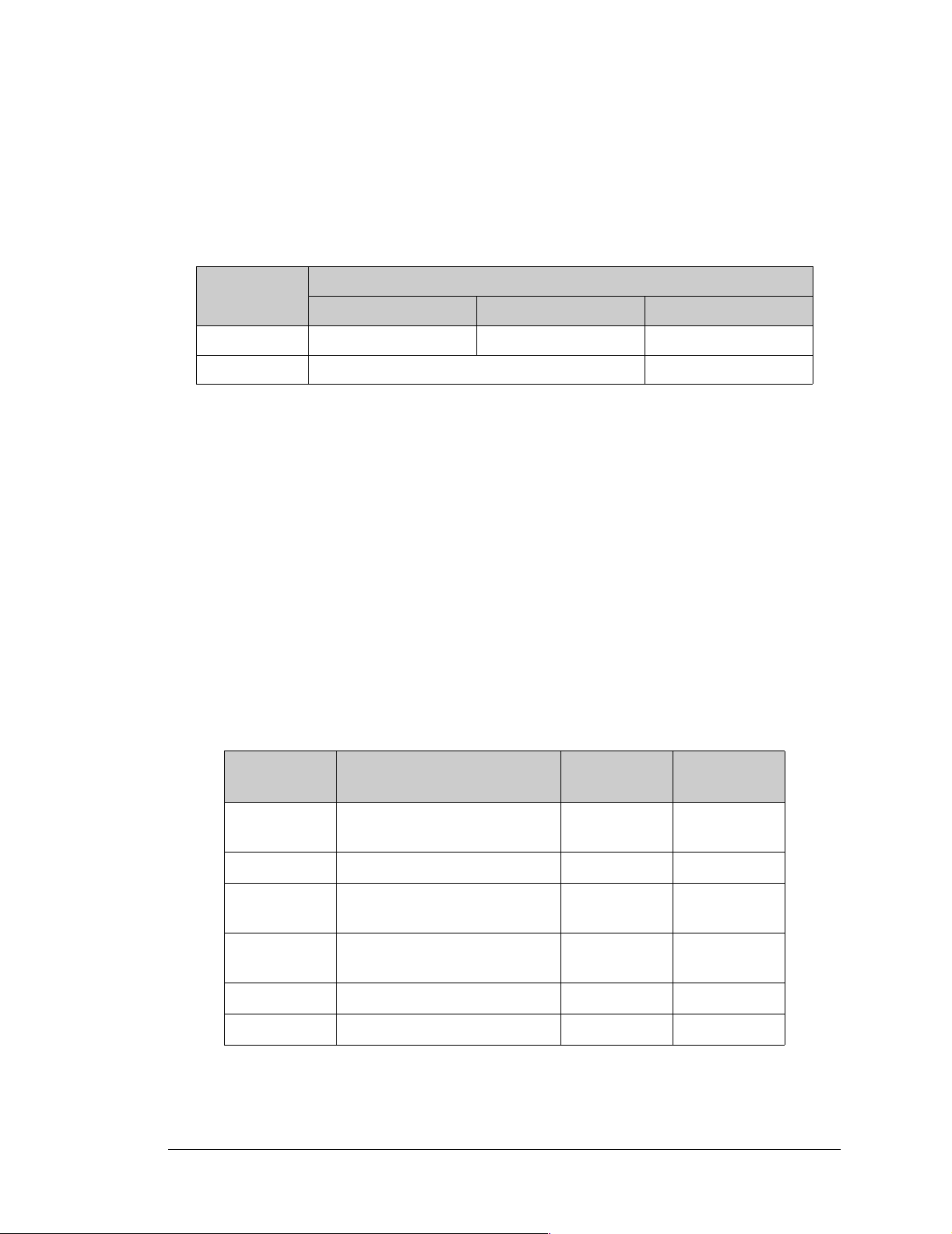
The LP3500 has three RS-232 serial ports that can set using the serMode software function
call as one RS-232 serial channel (with RTS/CTS) and one 3-wire channel, or they may be
set as three RS-232 (3-wire) channels. Table 4 summarizes the options.
Table 4. RS-232 Serial Communication Configurations
serMode
B C E
Serial Port
0 RS-232, 3-wire RS-232, 3-wire RS-232, 3-wire
1 RS-232, 5-wire CTS/RTS RS-232, 3-wire
The LP3500 also has one RS-485 serial channel (Serial Port F), one CMOS-level serial
interface port (Serial Port D), and one CMOS-level serial channel that serves as the programming port (Serial Port A).
All six serial ports operate in an asynchronous mode. An asynchronous port can handle 7
or 8 data bits. A 9th bit address scheme, where an additional bit is sent to mark the first
byte of a message, is also supported. Serial Port D and Serial Port A, the programming
port, can be operated alternately in the clocked serial mode. In this mode, a clock line synchronously clocks the data in or out. Either of the two communicating devices can supply
the clock. The LP3500 uses a 3.6864 MHz crystal, which is doubled to 7.3728 MHz. At
this frequency, the LP3500 supports standard asynchronous baud rates up to a maximum
of 921,600 bps.
Table 5 lists the use and the capabilities of the six serial ports.
Table 5. LP3500 Serial Port Uses and Capabilities
Serial Port Use
A
B 3-wire RS-232 J4 No
C
D
ERS-232 J4 No
FRS-485 J4 No
User’s Manual 25
Programming port or logic-level
serial port
3-wire RS-232 or RTS/CTS flow
control for Serial Port B
General-purpose serial interface
port
Header
Location
J5 Yes
J4 No
J6 Yes
Synchronous
Capability
Page 32

3.4.1 RS-232
The LP3500 RS-232 serial communication is supported by an RS-232 transceiver. This transceiver provides the voltage o utp ut, sl ew rate, and i npu t v oltage i mmuni ty requi red to meet
the RS-232 serial communicatio n p roto col. Bas ically, the chip translates the Rabbit 3000’s
logic-level signals to RS-2 32 s ig nal le vels. No te t hat the po lari ty is rever sed in an RS-23 2
circuit so that a +2.8 V out put becom es app roxi matel y -7 V and 0 V is out put as +7 V. The
RS-232 transceiver also provides t he p roper line l oading for reli able comm uni cation.
RS-232 can be used effectively at the LP3500’s m aximum baud rate for distances of up to
15 m.
Logic-level signals are also possible on Serial Ports B, C, and E by changing the 0 Ω
surface-mounted resistor jumper settings at locations JP1–JP6.
Serial Port E can be set to “listen” and “wake up” the LP3500 when the unit is in a lowpower mode.
3.4.2 RS-485
The LP3500 has one RS-485 serial channel, which is connected to Serial Port F on the
Rabbit 3000 through an RS-485 transceiver. The half-duplex communication uses the
Rabbit 3000’s PG0 pin to control the transmit enable on the communication line.
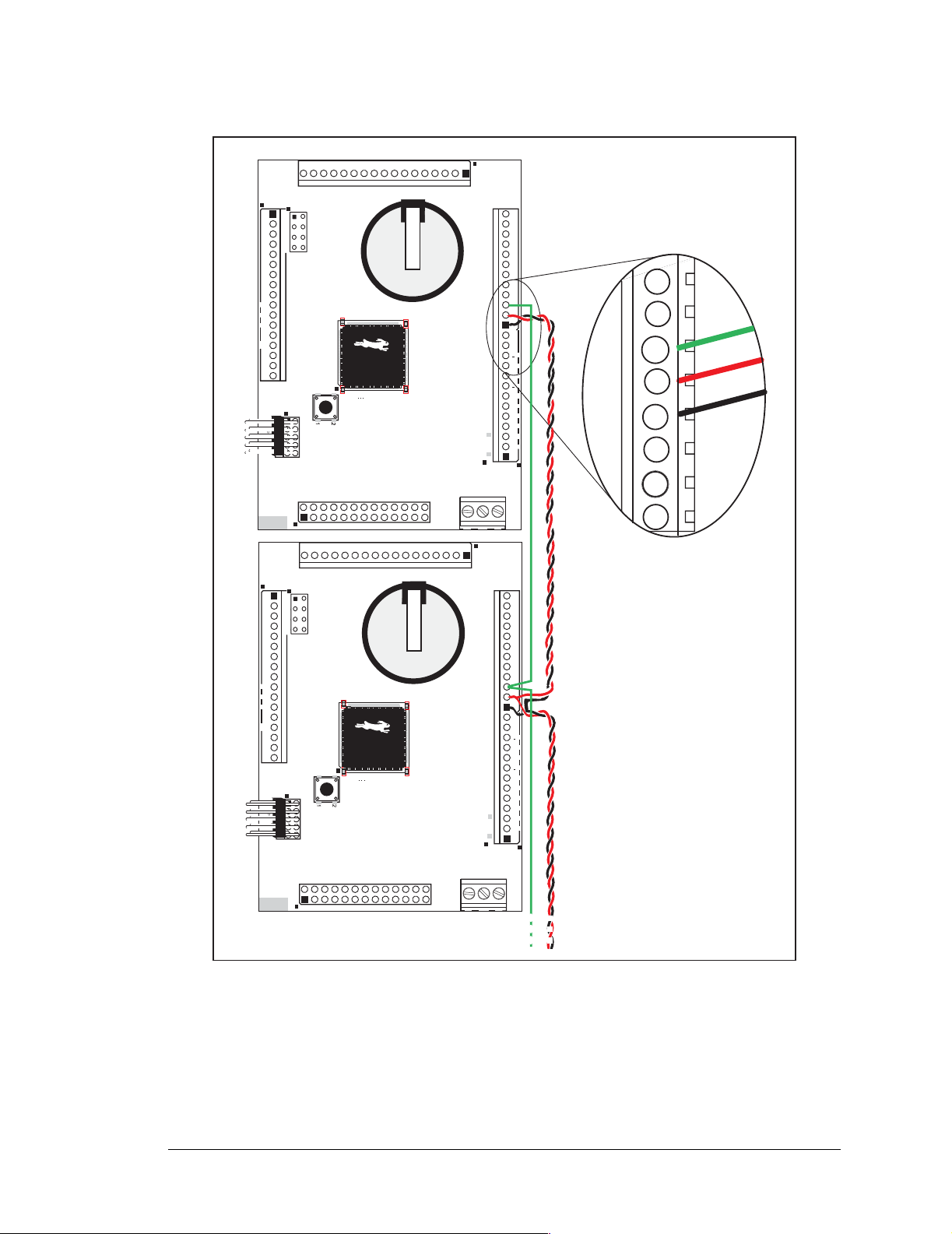
The LP3500 can be used in an RS-485 multidrop network. Connect the 485+ to 485+ and
485– to 485– using single twisted-pair wires (nonstranded, tinned) as shown in Figure 13.
Note that a common ground is recommended.
26 Fox (LP3500)
Page 33
IN00 IN01 IN02 IN03 IN04 IN05 IN06 IN07 GND IN08 IN09 IN10 IN11 IN12 IN13 IN14 IN15
J1
AIN0 AIN1 AIN2 AIN3 AIN4 AIN5 AIN6 AIN7 GND GND
PWM0
PWM1
PWM2
VBAT
EXT
GND VIN GND
J2
PROGRAM
PORT
GND
AIN0 AIN1 AIN2 AIN3 AIN4 AIN5 AIN6 AIN7 GND GND
PWM0
PWM1
PWM2
VBAT
EXT
GND VIN GND
PROGRAM
PORT
R1
AIN0 AIN1 AIN2 AIN3
J3
Battery
RESET
S1
J5
DISPLAY
R1
AIN0 AIN1 AIN2 AIN3
J3
NO
J4
Ground recommended
J4
Rx
4
+K GND 485 + GND TxB RxB GND TxC RxC GND TxE RxE GND
OUT9
OUT8
OUT7
OUT6
OUT5
OUT4
OUT3
OUT2
OUT1
OUT0
GND
J8
RELAY
NC
COM
IN00 IN01 IN02 IN03 IN04 IN05 IN06 IN07 GND IN08 IN09 IN10 IN11 IN12 IN13 IN14 IN15
J1
J4
3
2
1
13
2
TxB
GND
485+
485
+K
OUT9
OU
Battery
+K GND 485 + GND TxB RxB GND TxC RxC GND TxE RxE GND
OUT9
OUT8
J2
RESET
S1
J5
OUT7
OUT6
OUT5
OUT4
OUT3
OUT2
OUT1
OUT0
GND
GND
DISPLAY
J8
RELAY
NO
NC
COM
Figure 13. LP3500 Multidrop Network
Zener diodes are used in lieu of termination and bias resistors to minimize power consumption.
User’s Manual 27
Page 34
3.4.3 Serial Interface Port
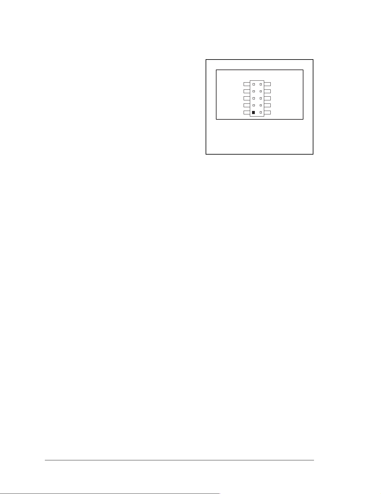
The LP3500 offers a Serial Interface port at header
J6, a 2 mm 2 × 5 socket. This port may be used to
connect serial logic-level devices such as Z-W orld’s
serial flash expansion cards to Serial Port D on the
Rabbit 3000.
Figure 14 provides the pinout for the Serial Interface Port.
PIO_2
PIO_1
PIO_0
PF0_SCK
PC1_SRX
J6
PF2_SRST
PB7_SFCS
PC0_STX
Vcc
GND
3.4.4 Programming Port
Figure 14. Serial Interface Port
(Header J6) Pinout
The LP3500 has a 10-pin programming header. The
programming port uses the Rabbit 3000’s Serial
Port A for communication, and is used for the following operations.
• Programming/debugging
• Cloning
The programming port is used to start the LP3500 in a mode where the LP3500 will do wnload a program from the port and then execute the program. The programming port transmits information to and from a PC while a program is being debugged.
The Rabbit 3000 startup-mode pins (SMODE0, SMODE1) are presented to the programming port so that an externally connected device can force the LP3500 to start up in an
external bootstrap mode. The LP3500 can be reset from the programming port via the
/EXT_RSTIN line.
The Rabbit 3000 status pin is also presented to the programming port. The status pin is an
output that can be used to send a general digital signal.
NOTE: Refer to the Rabbit 3000 Microprocessor User’s Manual for more information
related to the bootstrap mode.
28 Fox (LP3500)
Page 35
3.5 Display Interface
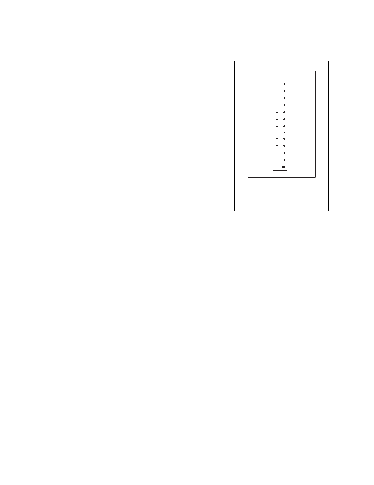
The LP3500 supports an interface with the parallel ports
on the Rabbit 3000 via the Display Interface at header
J9. The Display Interface may be used with Z-World’s
LCD/keypad module, which off ers an operator interface
with seven keys and a 122 × 32 graphic display.
Figure 15 provides the pinout for the Serial Interface
Port.
Appendix C, “LCD/Keypad Module,” provides further
information on the LCD/keypad module.
J9
BFD7
BFD5
BFD3
BFD1
BFA0
BFA2
GND
GND
LED5
LED3
LED1
DISP
VDISP
BFD6
BFD4
BFD2
BFD0
BFA1
BFA3
GND
LED6
LED4
LED2
LED0
DPRST
VDISP
Figure 15. Display Interface
(Header J9) Pinout
User’s Manual 29
Page 36
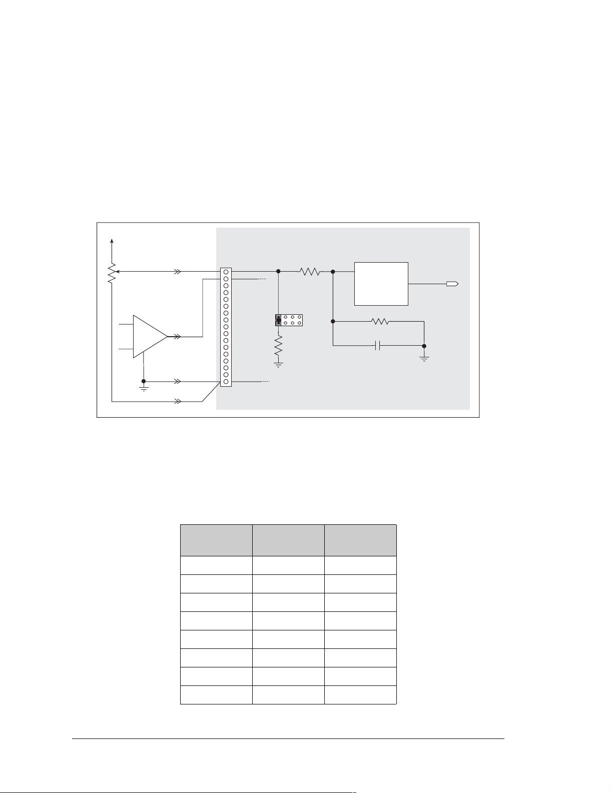
3.6 A/D Converter Inputs (LP3500 only)
The single 8-channel A/D converter chip used in the LP3500 (the LP3510 does not have
analog capabilities) has a resolution of 12 bits for differential measurements or 11 bits for
single-ended measurements. Four of the channels can be jumpered individually for 4–20 mA
using jumpers across pins on header J3, and all 8 channels can be used over several
software-scaled voltage ranges.
The
A/D converter chip has an internal amplifier that works with the resistor divider net-
work on the analog inputs as shown in
+ V
Figure 16.
AIN0
AIN1
R
IN
953 kW
ADC
Jumper pins to
configure for
420 mA
AGND
J3
100 W
52.3 kW
100 pF
Figure 16. Buffered A/D Converter Inputs
The
A/D converter chip can be programmed in software to operate over the voltage ranges
shown in
Table 6.
Table 6. A/D Converter Input Ranges
Gain Code Multiplier
0 1 0–20 V
1 2 0–10 V
2 4 0–5 V
Voltage
Range
3 5 0–4 V
4 8 0–2.5 V
5100–2 V
6160–1.25 V
7200–1 V
30 Fox (LP3500)
Page 37
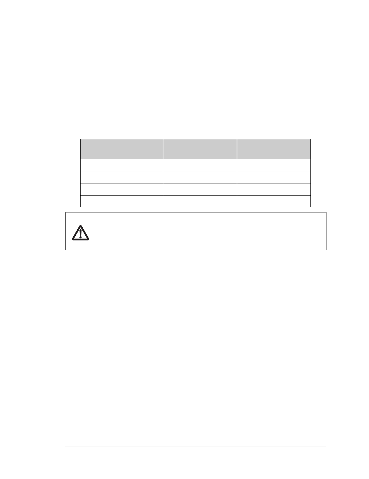
Single-ended measurements are made by connecting the analog signal between an analog
input channel (AIN0–AIN7) and AGND. Differential measurements are made by connecting a pair of differential analog signals to an adjacent pair of analog input channels
(AIN0–AIN1, …, AIN6–AIN7). The A/D converter is only capable of converting positve
voltages, and so will convert the difference between an adjacent pair of input channels,
and must be scaled for a voltage range appropriate for the voltage differences.
Table 7 lists the jumper configurations for header J3 used to set the 4–20 mA and the voltage measurement options.
Table 7. Header J3 Configuration for Analog I/O Options
Analog Input Channel
AIN0 Jumper “parked” on pin 2 Pins 1–2 connected
AIN1 Jumper “parked” on pin 4 Pins 3–4 connected
AIN2 Jumper “parked” on pin 6 Pins 5–6 connected
AIN3 Jumper “parked” on pin 8 Pins 7–8 connected
CAUTION: If you have enabled the 4–20 mA current option on any of the AIN0–AIN3
channels, be careful with any voltage sources that you might connect to these inputs.
The voltage must be le ss than 2.5 V to keep the current ac ross the 100 Ω resistor below
the maximum allowed current.
Voltage Option
(Factory Default)
4–20 mA Option
The A/D converter inputs are factory-calibrated, and the calibration constants are stored in
flash memory . You may calibrate the A/D converter inputs at a later time using the software
functions described in Section 4.5.5, “A/D Converter Inputs.”
NOTE: If you are using a fixed volt age ran ge, you should recalibr ate your LP35 00 at that
range.
AIN7 can be used to monitor Vcc using the VccMonitorInit function. While Vcc can
be monitored in all the power modes, Vcc monitoring is particularly useful when the
LP3500 is being operated from an external battery to monitor the voltage being supplied
by the battery.
The
VccMonitorInit function requires the operation of the A/D converter, which con-
sumes about 500 µA. The Vcc monitoring circuit itself consumes about 15 µA while it is
engaged.
Turn off VccMonitorInit (and the A/D converter if it is not going to be used)
when the test is done to extend your battery life.
User’s Manual 31
Page 38
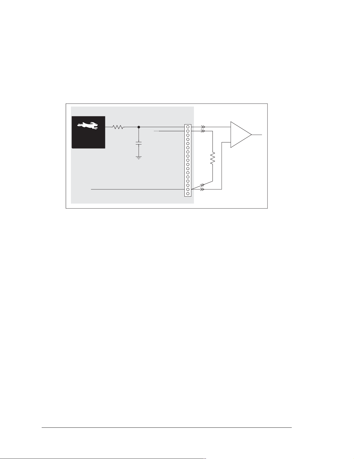
3.7 PWM Outputs
The D/A conversion outputs are pulse-width modulated and scaled to provide an output
from 0 V to Vcc (approx. 2.8 V).
Figure 17 shows the PWM outputs.
Rabbit 3000
Microprocessor
1 kW
PWM0
PWM1
1 nF
GND
Figure 17. PWM Outputs
32 Fox (LP3500)
Page 39
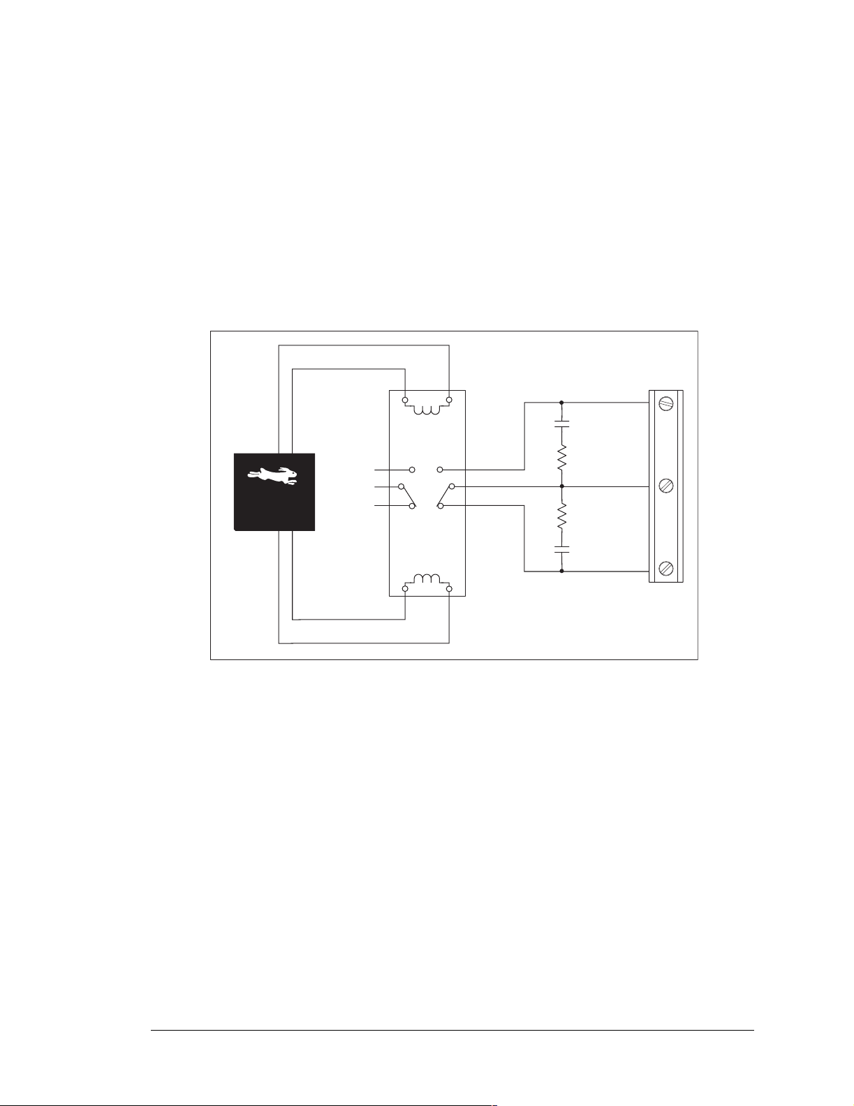
3.8 Relay Output Circuit (LP3500 only)
A bistable relay is stuffed on LP3500 models only at position K1, and the relay contacts
are accessed via screw-terminal header J8. The relay can switch up to 1 A at 30 V DC.
The relay is set via Parallel Port PG4 on the Rabbit 3000, and is reset via Parallel Port PG5
by a 10 ms pulse. The relay resets when the LP3500 resets, and operates only in the normal power modes.
NOTE: The relay does not reset automatically when power is removed from the
LP3500.
PG4
Rabbit 3000
Microprocessor
PG5
SET
RESET
5
-
10 nF
7
8
9
+
10
5.1 W
5.1 W
10 nF
1
+
4
3
2
-
6
NO
COM
NC
J8
1
2
3
Figure 18. Relay Output Circuit
NOTE: Switching the relay may consume up to 120 mA during the roughly 10 ms that it
takes for the relay to switch. Make sure that your power supply has sufficient capacity
to handle this sur ge c urrent to avoi d putti ng the LP3 500 into the power - save mode . The
relay does not consume any current while it is in the NO or the NC position and is not
switching.
User’s Manual 33
Page 40

3.9 Memory
3.9.1 SRAM
The LP3500 module is designed to accept 128K to 512K of SRAM packaged in an SOIC
case. The standard LP3500 modules come with 512K of SRAM.
3.9.2 Flash Memory
The LP3500 is also designed to accept 256K to 512K of flash memory packaged in a
TSOP case. The standard LP3500 modules comes with two 256K flash memory chips.
NOTE: Z-World recommends that any customer applications should not be constr ained
by the sector size of the flash memory since it may be necessary to change the sector
size in the future.
A Flash Memory Bank Se lect jump er configuration option based on 0 Ω surface-mounted
resistors exists at header JP10. This option, used in conjunction with some configuration
macros, allows Dynamic C to compile two different co-resident programs for the upper
and lower halves of the 256K flash in such a way that both programs start at logical
address 0000. This is useful for applications that require a resident download manager and
a separate downloaded program. See Technical Note 218, Implementing a Serial Down-
load Manager for a 256K Flash, for details.
34 Fox (LP3500)
Page 41

4. SOFTWARE
Dynamic C is an integrated development system for writing
embedded software. It runs on an IBM-compatible PC and is
designed for use with Z-World single-board computers and other
devices based on the Rabbit microprocessor.
Chapter 4 provides the libraries, function calls, and sample programs related to the LP3500.
You have a choice of doing your software development in the flash memory or in the static
RAM included on the LP3500. The advantage of working in RAM is to save wear on the
flash memory, which is limited to about 100,000 write cycles.
NOTE: An application can be developed in RAM, but cannot run standalone from RAM
after the programming cable is disconnected. All standalone applications can only run
from flash m emory.
The disadvantage of using flash memory for debug is that interrupts must be disabled for
approximately 5 ms whenever a break point is set in the program. This can crash fast interrupt routines that are running while you stop at a break point or single-step the program.
Flash memory or RAM is selected on the Options > Project Options > Compiler menu.
Dynamic C provides a number of debugging features. You can single-step your program,
either in C, statement by statement, or in assembly language, instruction by instruction.
You can set break points, where the program will stop, on any statement. Y ou can evaluate
watch expressions. A watch expression is any C expression that can be evaluated in the
context of the program. If the program is at a break point, a watch expression
expression using local or external variables.
User’s Manual 35
can view any
Page 42

4.1 Upgrading Dynamic C
4.1.1 Patches and Bug Fixes
Dynamic C patches that focus on bug fixes are available from time to time. C heck the Web
site
• www.zworld.com/support/
for the latest patches, workarounds, and bug fixes.
The default installation of a patch or bug fix is to install the file in a directory (folder) dif-
ferent from that of the original Dynamic C installation. Z-World recommends using a different directory so that you can verify the operation of the patch without overwriting the
existing Dynamic C installation. If you have made any changes to the BIOS or to libraries,
or if you have programs in the old directory (folder), make these same changes to the
BIOS or libraries in the new directory containing the patch. Do not simply copy over an
entire file since you may overwrite a bug fix; of course, you may copy over any programs
you have written. Once you are sure the new patch works entirely to your satisfaction, you
may retire the existing installation, but keep it available to handle legacy applications.
4.1.2 Upgrades
Dynamic C installations are designed for use with the board they are included with, and
are included at no charge as part of our low-cost kits. Dynamic C is a complete software
development system, but does not include all the Dynamic C features. Z-W orld also offers
add-on Dynamic C modules containing the popular µC/OS-II real-time operating system,
as well as PPP, Advanced Encryption Standard (AES), and other select libraries. In addition to the Web-based technical support included at no extra charge, a one-year telephonebased technical support module is also available for purchase.
36 Fox (LP3500)
Page 43
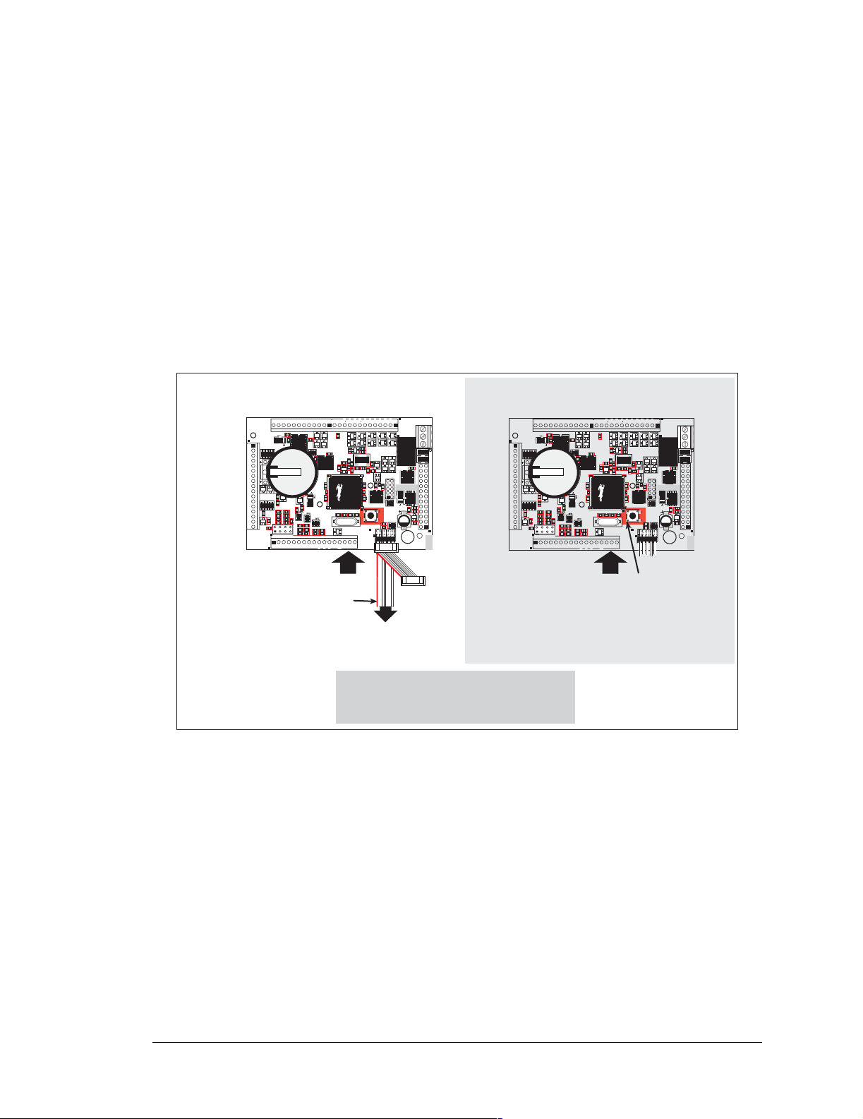
4.2 Programming Cable
The programming cable has a level converter board in the middle of the cable since the
LP3500 programming port supports CMOS logic levels, and not the higher voltage RS-232
levels that are used by PC serial ports. When the programming cable is connected,
Dynamic C running on the PC can hard-reset the LP3500 and cold-boot it. The cold boot
includes compiling and downloading a BIOS program that stays resident while you work. If
you crash the target, Dynamic C will automatically reboot and recompile the BIOS if it
senses that a target communication error occurred or that the BIOS source code has changed.
4.2.1 Switching Between Program Mode and Run Mode
The LP3500 is automatically in Program Mode when the programming cable is attached,
and is automatically in Run Mode when no programming cable is attached. See Figure 19.
J4
J1
IN00 IN01 IN02 IN03 IN04 IN05 IN06 IN07 GND IN08 IN09 IN10 IN11 IN12 IN13 IN14 IN15
RN2
C6
D4
D2
C10 C13
C2
RN1
C3
R6
R7
R9
D1
R1
AIN0 AIN1 AIN2 AIN3
AIN0 AIN1 AIN2 AIN3 AIN4 AIN5 AIN6 AIN7 GND GND
C15
C12
D5
D11
D7
C8
D8
R13
R16
R17
Program Mode
OUT9
OUT8
OUT7
OUT6
+K GND 485 + GND TxB RxB GND TxC RxC GND TxE RxE GND
D19
D20
D26
C16
C19
C20
Q22
Colored edge
R37
U1
D15 D17
C22
D13
R23
R30
C24
R18
C26
R20
J3
R22
C36
RP17
R57
Battery
R31
C29
C33
R29
R25
C37
R26
D25
Q8
Q5
R42
D21
D18
R38
C48
Q6
C53
C51
R34
R41
R39
R44
C55
U3
U8
C43
BT1
C44
R40 C54
R36
C50
Y1
R32
C40
D22
J2
PWM1
PWM2
PWM0
VBAT
GND VIN GND
EXT
Power
OUT2
OUT5
OUT4
OUT3
D30
D28
Q16
Q10
R43
R33
Q13
Y2
C61
Q12
R47
R45
U11
C59
R48
C60
U10
U9
RP13
S1
RESET
R50
R49
J5
PROGRAM
PORT
OUT1
OUT0
GND
J8
RELAY
D34
Q17
K1
D32
C67
U12
D33Q14
J6
C66
J9
C64
U13
C70
R51
R58
C65
Q20
R54
RP14
PROG
GND
DIAG
Programming
Cable
NC
COM
NO
R56
R55
DISPLAY
J4
J1
IN00 IN01 IN02 IN03 IN04 IN05 IN06 IN07 GND IN08 IN09 IN10 IN11 IN12 IN13 IN14 IN15
RN2
D4
D2
C2
RN1
C3
R6
R7
R9
D1
R1
AIN0 AIN1 AIN2 AIN3
AIN0 AIN1 AIN2 AIN3 AIN4 AIN5 AIN6 AIN7 GND GND
C15
C12
D5
D7
C6
C8
D8
C10 C13
R17
C16
U1
C19
D15 D17
C20
C22
D11
D13
R23
Q22
R30
C24
R13
R16
R18
C26
R20
J3
R22
Run Mode
+K GND 485 + GND TxB RxB GND TxC RxC GND TxE RxE GND
D19
D20
R37
C36
D21
D18
RP17
C48
R57
Battery
C51
R31
R34
U3
U8
C29
C43
BT1
C44
C50
Y1
C33
R29
R32
R25
C40
C37
R26
PWM1
PWM2
PWM0
VBAT
EXT
Power
OUT9
D25
R36
D22
GND VIN GND
OUT1
OUT0
OUT8
OUT2
OUT5
OUT4
OUT3
OUT7
OUT6
GND
J8
RELAY
D30
D28
D26
D34
Q8
Q5
R42
Q17
Q16
Q10
R43
R33
R38
Q6
Q13
Y2
C53
C61
Q12
R41
R39
R44
C55
R47
R45
U11
J6
C66
C59
R48
C60
U10
U9
RP13
S1
R40 C54
RESET
R50
R49
J5
J2
PROGRAM
PORT
RESET
switch
NC
COM
NO
K1
R56
D32
R55
C67
U12
D33Q14
J9
DISPLAY
C64
U13
C70
R51
R58
C65
Q20
R54
RP14
GND
To
PC COM port
RESET LP3500 when changing mode:
Press RESET switch,
Remove, then reapply power
after removing or attaching programming cable.
OR
Figure 19. LP3500 Program Mode and Run Mode Set-Up
4.2.2 Detailed Instructions: Changing from Program Mode to Run Mode
1. Disconnect the programming cable from header J3 of the LP3500.
2. Reset the LP3500 by unplugging the AC adapter, then plugging it back in, or press the RESET
switch.
The LP3500 is now ready to operate in the Run Mode.
4.2.3 Detailed Instructions: Changing from Run Mode to Program Mode
1. Attach the programming cable to header J1 of the LP3500.
2. Reset the LP3500 by unplugging the AC adapter, then plugging it back in, or press the RESET
switch. Alternatively, you may press <Ctrl-Y> on your PC if Dynamic C is running.
The LP3500 is now ready to operate in the Program Mode.
User’s Manual 37
Page 44

4.3 Sample Programs
Sample programs are provided in the Dynamic C Samples folder. The sample program
PONG.C demonstrates the output to the STDIO window.
The various directories in the Samples folder contain specific sample programs that illustrate the use of the corresponding Dynamic C libraries.
The LP3500 folder provides sample programs specific to the LP3500. Each sample program has comments that describe the purpose and function of the program. Follow the
instructions at the beginning of the sample program.
To run a sample program, open it with the File menu (if it is not still open), compile it
using the Compile menu, and then run it by selecting Run in the Run menu. The LP3500
must be in the Program mode (see Section 4.2, “Programming Cable”) and must be connected to a PC using the programming cable as described in Section 2.1, “LP3500 Connections.”
Appendix G, “Running a Sample Program,” takes you through the steps of running one of
the sample programs.
4.3.1 Power Modes
The following sample program is found in the POWER subdirectory in SAMPLES\LP3500.
• POWER.C—This program demonstrates switching from the normal raw DC power
source to an external battery using the Prototyping Board. Pressing a switch will
change from the power source and will be displayed by flashing LEDs.
• LOWPWRDEMO.C—This program demonstrates a low-power mode with the normal power
source connected to the LP3500.
4.3.2 Digital I/O
The following sample programs are found in the IO subdirectory in SAMPLES\LP3500.
• DIGIN.C—Demonstrates the use of the digital inputs. Using the Prototyping Board, you
can see an input channel toggle from HIGH to LOW when pressing a pushbutton on the
Prototyping Board.
• DIGOUT.C—Demonstrates the use of the high-current outputs configured as either sinking or sourcing outputs. Using the Prototyping Board, you can see an LED toggle
on/off via a high-current output.
• DIGBANKIN.C—Demonstrates the use of the digital inputs. Using the Prototyping
Board, you can see a bank of input channels toggle from HIGH to LOW when pressing
a pushbutton on the Prototyping Board.
• DIGBANKOUT.C—Demonstrates the use of the high-current outputs configured as either
sinking or sourcing outputs. Using the Prototyping Board, you can see a bank of channels toggle the corresponding LEDs on/off via high-current outputs.
38 Fox (LP3500)
Page 45

4.3.3 Serial Communication
The following sample programs are found in the RS232 subdirectory in SAMPLES\LP3500.
SIMPLE3WIRE.C—This program demonstrates basic initialization for a simple RS-232
•
3-wire loopback displayed in the
STDIO window.
The following sample programs are found in the RS485 subdirectory in SAMPLES\LP3500.
SIMPLE485MASTER.C—This program demonstrates a simple RS-485 transmission of
•
lower case letters to a slave LP3500. The slave will send back converted upper case letters back to the master LP3500 and display them in the STDIO window. Use
SIMPLE485SLAVE.C to program the slave LP3500.
• SIMPLE485SLAVE.C—This program demonstrates a simple RS-485 transmission of
lower case letters to a slave LP3500. The slave will send back converted upper case letters back to the master LP3500 and display them in the STDIO window. Use
SIMPLE485MASTER.C to program the master LP3500.
4.3.4 A/D Converter Inputs
The following sample programs are found in the ADC subdirectory in SAMPLES\LP3500.
• AD_RDVOLT_ALL.C—This program reads and displays the voltage and equivalent values
of each single-ended A/D converter channel. Coefficients are read from the A/D converter's simulated EEPROM in flash memory to compute the equivalent voltages. Computed raw data and equivalent voltages are displayed in the STDIO window.
• AD_RDVOLT_CH.C—This program reads and displays the voltage and equivalent values
of one single-ended A/D converter channel. Coefficients are read from the A/D converter's simulated EEPROM in flash memory to compute the equivalent voltages. Computed raw data and equivalent voltages are displayed in the STDIO window.
• AD_RDDIFF_CH.C—This program demonstrates reading one differential A/D converter
channel. Coefficients are read from the A/D converter's simulated EEPROM in flash
memory to compute the equivalent voltages. Computed raw data and equivalent voltages are displayed in the STDIO window.
• AD_RDMA_CH.C—This program demonstrates reading one milliampere A/D converter
channel. Coefficients are read from the A/D converter's simulated EEPROM in flash
memory to compute the equivalent currents. Computed raw data and equivalent currents are displayed in the STDIO window.
• AD_SAMPLE.C—This program demonstrates how to use the A/D low-level driver. The
program will display the average voltage that is present on an A/D converter channel.
The particular channel and the number of samples may be changed by the user.
User’s Manual 39
Page 46

4.3.5 PWM Outputs
The following sample program is found in the IO subdirectory in SAMPLES\LP3500.
• PWMOUT.C—This program demonstrates the PWM functions. It will set the PWM channels, PWM0–PWM2, to the following duty cycles:
PWM Channel 0 to 10%
PWM Channel 1 to 25%
PWM Channel 2 to 50%
All activity will be displayed in the
STDIO window.
4.3.6 Relay Output
The following sample program is found in the RELAY subdirectory in SAMPLES\LP3500.
• SWRELAY.C—This program demonstrates the relay-switching function call operating on
normal power source. Use the pushbutton switches on the Prototyping Board to switch
the relay between the SET (NO) and RESET (NC) positions. All activity will be displayed with the LEDs.
4.3.7 Vcc Monitoring
The following sample program is found in the POWER subdirectory in SAMPLES\LP3500.
• VCCMONITOR.C—This program demonstrates the Vcc monitoring function on AIN7.
All activity will be displayed in the STDIO window
4.3.8 LP3500 Calibration
The following sample programs are found in the ADC subdirectory in SAMPLES\LP3500.
• ADCAL_ALL.C—This program demonstrates how to recalibrate all single-ended A/D
converter channels using two known voltages to generate constants for each channel,
and will be written into the user block data area. The program uses the STDIO window
to display the voltage that is being monitored.
NOTE: This sample program will overwrite the calibration constants set at the factory.
• ADCAL_CHAN.C—This program demonstrates how to recalibrate one single-ended A/D
converter channel using two known voltages to generate constants for each channel,
and will be written into the user block data area. The program uses the STDIO window
to display the voltage that is being monitored.
NOTE: This sample program will overwrite the calibration constants set at the factory.
• AD_CALDIFF.C—This sample program demonstrates how to recalibrate one dif fe rential
A/D converter channel using two known voltages to generate constants for that channel
and rewrite the constants into the user block data area. The program uses the STDIO
window to display the voltage that is being monitored.
NOTE: This sample program will overwrite the calibration constants set at the factory.
40 Fox (LP3500)
Page 47

• AD_CALMA_CH.C—This sample program demonstrates how to recalibrate one A/D converter channel operating in the 4–20 mA current mode using two known currents to
generate two coefficients, gain and offset, which are rewritten into the user block data
area. The program uses the STDIO window to display the current that is being monitored.
NOTE: This sample program will overwrite the calibration constants set at the factory.
4.3.9 LCD/Keypad Module Sample Programs
Sample programs for the LCD/keypad module are described in Section C.8.
User’s Manual 41
Page 48
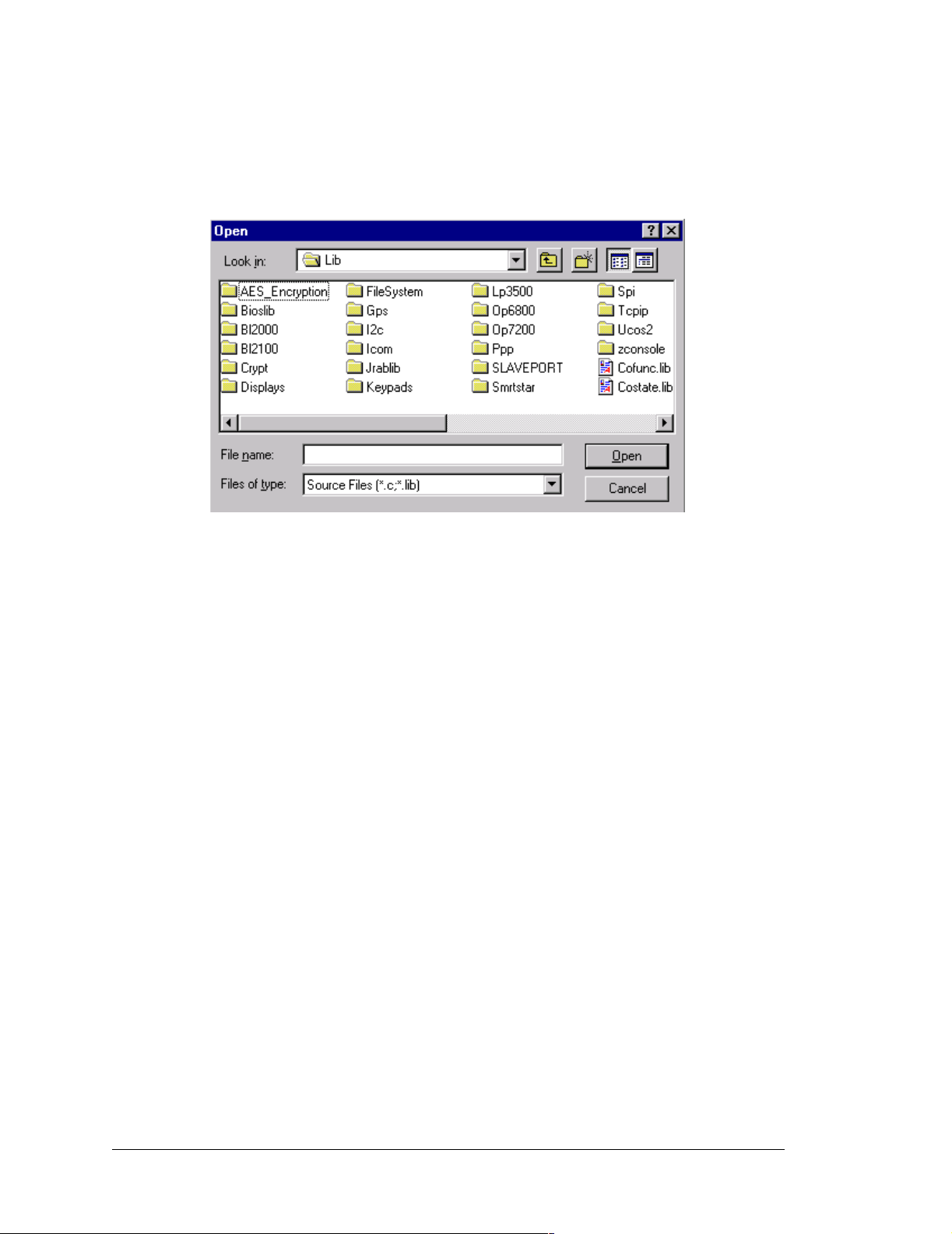
4.4 LP3500 Libraries
With Dynamic C running, click File > Open, and select Lib. The following list of
Dynamic C libraries and library directories will be displayed.
Two library directories provide libraries of function calls that are used to develop applications for the LP3500.
• LP3500—libraries associated with features specific to the LP3500. The functions in the
LP35xx.LIB library are described in Section 4.5, “LP3500 Function APIs.”.
Two other library directories provide libraries of function calls that are used to develop
applications for the optional LCD/keypad module.
• DISPLAYS\GRAPHIC—libraries associated with LCD display.
• KEYPADS–libraries associated with the keypad.
The LCD/keypad module functions are described in Section C.7. Other generic functions
applicable to all devices based on the Rabbit 3000 microprocessor are described in the
Dynamic C User’s Manual.
42 Fox (LP3500)
Page 49
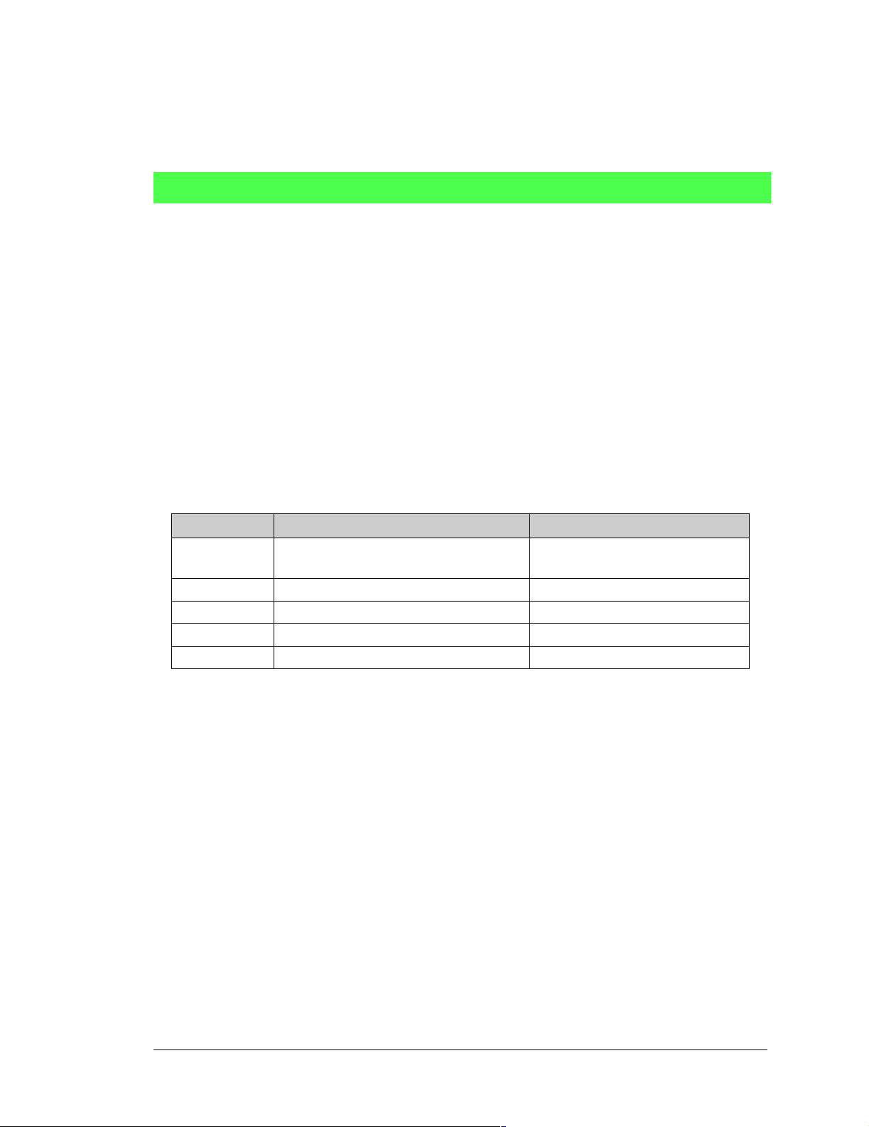
4.5 LP3500 Function APIs
4.5.1 LP3500 Power Modes
int devPowerSet(int devices, int state);
Sets individual devices to low-power or fully active states in the order listed below.
PARAMETERS
devices is a list of the following macros, which are OR'ed together, that will be af fected by the state
parameter, e.g., RS232DEV|ADCDEV.
RS232DEV—RS-232 devices
RS485DEV—RS-485 devices
ADCDEV—ADS7870 A/D converter devices
DISPDEV—LCD/keypad module
ALLDEVICES—all devices
state
0 = shuts or powers down listed devices
1 = activates listed devices
Macro Description state = 0 state after Board Initialization
RS232DEV
RS485DEV Transmitter is disabled 0
ADCDEV ADS7870 internal oscillator is turned off 0
DISPDEV LCD/keypad module is turned off. 0
ALLDEVICES All devices are disabled as described above —
Table E-1 provides further information about the power consumption associated with each section.
RETURN VALUE
0 if valid parameter
-1 otherwise
SEE ALSO
powerMode, anaInConfig, brdInit
Receivers and transmitters are disabled,
RxE remains active
1
User’s Manual 43
Page 50
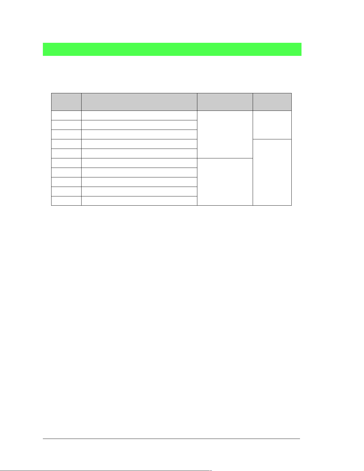
int powerMode(int mode);
Sets the LP3500 operating power.
PARAMETERS
mode is the operating mode based on the following macros.
Mode Description
1 CCLK = PCLK = MainOsc = 7.3728 MHz
3 CCLK = PCLK = MainOsc/4 = 1.8423 MHz
4 CCLK = PCLK = MainOsc/6 = 1.2288 MHz
5 CCLK = PCLK = MainOsc/8 = 0.9216 MHz
6 CCLK = PCLK = 32.768 kHz
7 CCLK = PCLK = 32.768 kHz/2 = 16.384 kHz
8 CCLK = PCLK = 32.768 kHz/4 = 8.192 kHz
9 CCLK = PCLK = 32.768 kHz/8 = 4.096 kHz
10 CCLK = PCLK = 32.768 kHz/16 = 2.048 kHz
Typi cal Curre n t
Consumption
5–16 mA
2 mA
Debug
Capable?
Yes2 CCLK = PCLK = MainOsc/2 = 3.6864 MHz
No
NOTE: When using modes 6–10, be sure to call hitwd() expl icitly since periodic inte r-
rupts, which incorporate a virtual watchdog, are disabled in these modes.
Table 2 provides more specific information on the LP3500’s capabilities associated with these and other
software-defined modes.
RETURN VALUE
0 if valid parameter
-1 if invalid parameter
SEE ALSO
devPowerSet, rdPowerState, setPowerState, VccMonitor
44 Fox (LP3500)
Page 51

void serCommAlert(int lowpowermode, int
maxpowermode, int powersource, unsigned long
timeout);
Use this function to poll Serial Port E for any activity or until a timeout occurs. The function call forces
the LP3500 to enter the low-power mode using the battery for polling. Upon expiration of the timeout or
the receipt of a serial byte, this function will enable the normal power mode and exit.
Use devPowerSet(ALLDEVICES, int state) before and after this function call to deactivate
and activate all devices to operate at less power.
PARAMETERS
lowpowermode is the low-power mode setting to enter, usually 10 (see powerMode())
maxpowermode is the maximum operating power mode setting to enter, usually 1 (see power-
Mode())
powersource
1 = battery
2 = raw DC power
timeout is the timeout in seconds if no activity is detected on the RxE receiver line. Enter 0 for no
timeout
SEE ALSO
powerMode, digInAlert, timedAlert, devPowerSet
void timedAlert(int lowpowermode, int maxpowermode,
int powersource, unsigned long timeout)
Use this function to poll the real-time clock until a timeout occurs. The function call forces the LP3500 to
enter the low-power mode, disables the normal power source, and may enable the external battery for
polling. Upon expiration of the timeout this function will enable the normal power mode and exit. If the
normal power source is not available, the LP3500 will not be able to rsume operation at the maximumpower mode, and may reset.
Use devPowerSet(ALLDEVICES, int state) before and after this function call to deactivate
and activate all devices to operate at less power.
PARAMETERS
lowpowermode is the low-power mode setting to enter, usually 10 (see powerMode())
maxpowermode is the maximum operating power mode setting to enter, usually 1 (see power-
Mode())
powersource
1 = battery
2 = raw DC power
timeout is the timeout in seconds if an input is not received.
SEE ALSO
powerMode, digInAlert, serCommAlert, devPowerSet
User’s Manual 45
Page 52

void digInAlert(int channel, int value, int
lowpowermode, int maxpowermode, int powersource,
unsigned long timeout)
Use this function to poll a selected digital input until a timeout occurs. The function call forces the
LP3500 to enter the low-power mode using the battery for polling. Upon activation of the channel or
expiration of the timeout, this function will enable the normal power mode and exit.
Use devPowerSet(ALLDEVICES, int state) before and after this function call to deactivate
and activate all devices to operate at less power.
PARAMETERS
channel is the digital input channel (IN00– IN15) to poll
value is the input value of 0 or 1 to receive
lowpowermode is the low-power mode setting to enter, usually 10 (see powerMode())
maxpowermode is the maximum operating power mode setting to enter, usually 1 (see power-
Mode())
powersource
1 = battery
2 = raw DC power
timeout is the timeout in seconds if an input is not received. Enter 0 for no timeout.
SEE ALSO
powerMode, serCommAlert, timedAlert, devPowerSet
int rdPowerState(void);
Determines if the LP3500 is running under battery power or a raw DC power source.
RETURN VALUE
0 if on raw DC power source
1 if on battery power
SEE ALSO
powerMode, setPowerState
int setPowerSource(int state);
Turns the linear regulator “off” or “on.”
PARAMETER
0 for normal power source
1 for battery
RETURN VALUE
0 if successful
-1 if raw DC power source is not available
-2 if battery is not available
SEE ALSO
powerMode, rdPowerState
46 Fox (LP3500)
Page 53

4.5.2 Board Initialization
void brdInit (void);
Call this function at the beginning of your program. This function initializes the system I/O ports and
loads all the A/D converter and D/A converter calibration constants from flash memory into SRAM for
use by your program. If the LCD/keypad module is installed, this function will turn off LED DS1 to indicate that the initialization was successful.
Summary of Initialization
• LP3500 uses main oscillator
• LCD/keypad module buffer is disabled
• RS-485 serial communication is not enabled
• RS-232 serial communication is enabled
• Unused configureable inputs are tied and unused configureable outputs are set low
• Self-timed chip select is s e t to 109 ns
• If A/D converter chip is inst alled, chip is reset and SCLKD is set to 19,200 bps
• If A/D converter chip is inst alled, calibration constants are read
• If relay is installed, relay is set to NC or RESET position
The ports are initialized according to Table A-3.
User’s Manual 47
Page 54

4.5.3 Digital I/O
void digOut(int channel, int value);
Sets the state of a digital output (OUT0–OUT9).
Remember to call brdInit before executing this function.
A runtime error will occur for the following conditions:
1. channel or value out of range.
2. brdInit was not executed before executing digOut.
PARAMETERS
channel is the output channel number (0–9).
value is the output value (0 or 1).
SEE ALSO
brdInit, digIn, digBankOut
void digBankOut(int bank, int value);
Writes the state of a block of designated digital output channels. The first bank consists of OUT0–
OUT7, the second bank consists of OUT8–OUT9.
A run-time error will occur for the following conditions:
1. channel or value out of range.
2. brdInit was not executed before executing digOut.
PARAMETER
bank is 0 for OUT0–OUT7, 1 for OUT8–OUT9.
value is an 8-bit output value, where each bit corresponds to one channel. OUT0 and OUT8 are the
least significant bit 0.
RETURN VALUE
None.
SEE ALSO
brdInit, digOut, digBankIn
48 Fox (LP3500)
Page 55

int digIn(int channel);
Reads the state of an input channel (IN00–IN15).
A run-time error will occur for the following conditions:
1. channel out of range.
2. brdInit was not executed before executing digIn.
PARAMETER
channel is the input channel number (0–15)
RETURN VALUE
The logic state of the input (0 or 1).
SEE ALSO
brdInit, digOut, digBankIn
void digBankIn(int bank);
Reads the state of a block of designated digital input channels. The first bank consists of IN0–IN07, the
second bank consists of IN08–IN15.
A run-time error will occur for the following conditions:
1. bank out of range.
2. brdInit was not executed before executing digIn.
PARAMETER
bank is 0 for IN00–IN07, 1 for IN08–IN15.
RETURN VALUE
An input value in the lower byte, where each bit corresponds to one channel. IN00 and IN08 are in the
bit 0 place.
SEE ALSO
brdInit, digOut, digBankOut
User’s Manual 49
Page 56
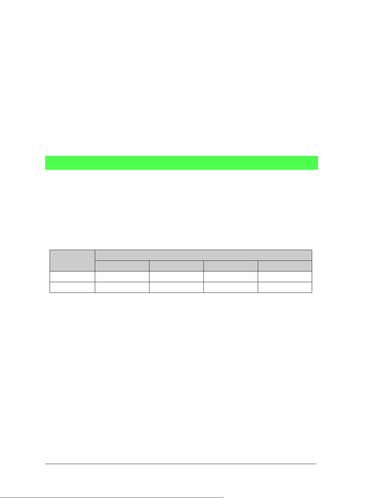
4.5.4 Serial Co mmunication
Library files included with Dynamic C provide a full range of serial communications support. The RS232.LIB library provides a set of circular-buffer-based serial functions. The
PACKET.LIB library provides packet-based serial functions where packets can be delim-
ited by the 9th bit, by transmission gaps, or with user-defined special characters. Both
libraries provide blocking functions, which do not return until they are finished transmitting or receiving, and nonblocking functions, which must be called repeatedly until they
are finished. For more information, see the Dynamic C User’s Manual and Technical
Note TN213, Rabbit 2000 Serial Port Softwar
e.
Use the following function calls with the LP3500.
int serMode(int mode);
User interface to set up LP3500 serial communication lines. Call thi s f unction after serXOpen().
Whether you are opening one or multiple serial po rts, this function must be executed after execut ing the last
serXOpen function AND before you start using any of the serial ports. This function is non-reentrant.
If Mode 1 is selected, CTS/RTS flow control is exercised using the serBflowcontrolOn and
serBflowcontrolOff functions from the RS232.LIB library.
PARAMETER
mode is the defined serial port configuration.
Mode
0 RS-232, 3-wire RS-232, 3-wire RS-232, 3-wire RS-485
1 RS-232, 5-wire CTS/RTS RS-232, 3-wire RS-485
RETURN VALUE
0 if valid mode, 1 if not.
SEE ALSO
ser485Tx, ser485Rx
Serial Port
B C E F
50 Fox (LP3500)
Page 57

void ser485Tx(void);
Enables the RS-485 transmitter. Transmitted data get echo'ed back into the receive data buffer. These
echo'ed data could be used to know when to disable the transmitter by using one of the following
methods:
Byte mode—disable the transmitter after the same byte that is transmitted is detected in the receive
data buffer.
Block data mode—disable the transmitter after the same number of bytes transmitted is detected in the
receive data buffer.
serMode() must be executed before running this function.
SEE ALSO
serMode, ser485Rx
void ser485Rx(void);
Disables the RS-485 transmitter. This puts the LP3500 in listen mode, which allows it to receive data
from the RS-485 interface. serMode() must be executed before running this function.
SEE ALSO
serMode, ser485Tx
User’s Manual 51
Page 58
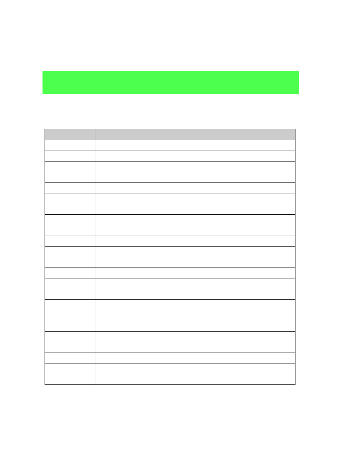
4.5.5 A/D Converter Inputs
The functions in this section apply only to the LP3500 model.
unsigned int anaInConfig(unsigned int
instructionbyte, unsigned int cmd, long baud);
Use this function to configure the ADS7870 A/D converter. This function will address the ADS7870 in
Register Mode only, and will report an error if you try to use it in Di rect Mod e . Refer to AD S787 0 specification for proper addressing and commands.
ADS7870 Signal ADS7870 State LP3500 Function/State
LN0 Input AIN0
LN1 Input AIN1
LN2 Input AIN2
LN3 Input AIN3
LN4 Input AIN4
LN5 Input AIN5
LN6 Input AIN6
LN7 Input AIN7
/RESET Input Board reset device
RISE/FALL Input Tied up for SCLK active on rising edge
PIO_0 Input Pulled down unless driven by serial interface connection
PIO_1 Input Pulled down unless driven by serial interface connection
PIO_2 Input Pulled down unless driven by serial interface connection
PIO_3 Input Pulled up unless driven by Vcc monitor
CONVERT Input Pulled down, not used
BUSY Output PF1 pulled down; 1 state converter is busy
CCLKCNTRL Input Tied down; 0 state sets CCLK as input
CCLK Input Tied down; external conversion clock
SCLK Input PF0; serial data transfer clock
SDI Input PC0; 3-wire mode for serial data input
SDO Output PC1; serial data output /CS driven
/CS Input PF3 pulled up; active-low enables serial interface
BUFIN Input Tied down; reference buffer amplifier
52 Fox (LP3500)
Page 59

PARAMETERS
instructionbyte will initiate a read or write operation at 8 or 16 bits on the designated register
address, for example:
checkid = anaInConfig(0x5F, 0, 9600); // read ID and set baud rate
cmd is the command data that configure the registers addressed by the instruction byte. Enter 0 if per-
forming a read operation.
i = anaInConfig(0x07, 0x3a, 0); // write ref/osc reg and enable
baud is the serial clock transfer rate of 9600 to 57,600 bps. baud must be set on the first call to this
function. Enter 0 in this parameter thereafter.
anaInConfig(0x00, 0x00, 9600); // resets device and sets baud
RETURN VALUE
0 on write operations, data value on read operations.
SEE ALSO
anaInDriver, anaIn, brdInit
User’s Manual 53
Page 60
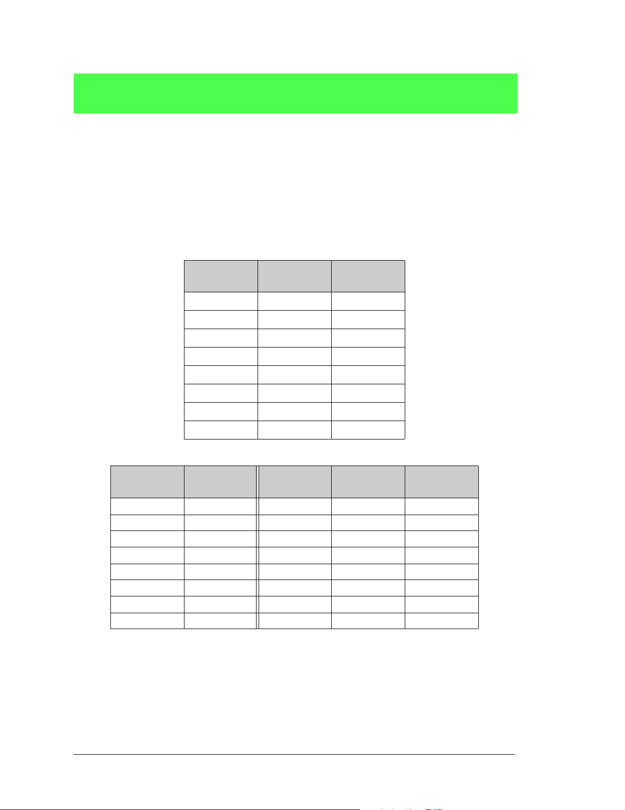
unsigned int anaInDriver(unsigned int cmd,
unsigned int len);
Reads the voltage of an analog input channel by serial-clocking an 8-bit command to the ADS7870
device by its Direct Mode method. The conversion begins as soon as the last data bit is transferred.
An exception error will occur if Direct Mode bit D7 is not set.
PARAMETER
cmd contains a gain code and a channel code as follows.
D7—1; D6–D4—Gain Code; D3–D0—Channel Code
Use the following calculation and the tables below to determine cmd:
cmd = 0x80 | (gain_code*16) + channel_code
Channel Code
0 +AIN0 -AIN1 8 AIN0 AIN0
1 +AIN2 -AIN3 9 AIN1 AIN1
2 +AIN4 -AIN5 10 AIN2 AIN2
3 +AIN6 -AIN7 11 AIN3 AIN3
4 Reserved 12 AIN4 Reserved
5 Reserved 13 AIN5 Reserved
6 Reserved 14 AIN6 Reserved
7 Reserved 15 AIN7 Reserved
Gain Code Multiplier
0 1 0–20 V
1 2 0–10 V
2 4 0–5 V
3 5 0–4 V
4 8 0–2.5 V
5100–2 V
6160–1.25 V
7200–1 V
Differential
Input Lines
Channel Code
Voltage
Range
Single-Ended
Input Lines
*
4–20 mA
Lines
* Negative input is ground.
len, the output bit length, is always 12 bits.
54 Fox (LP3500)
Page 61

RETURN VALUE
A value corresponding to the voltage on the analog input channel, which will be:
0–2047 for 11-bit A/D conversions (bit 12 for sign)
-1 for overflow
SEE ALSO
anaInConfig, anaIn
User’s Manual 55
Page 62
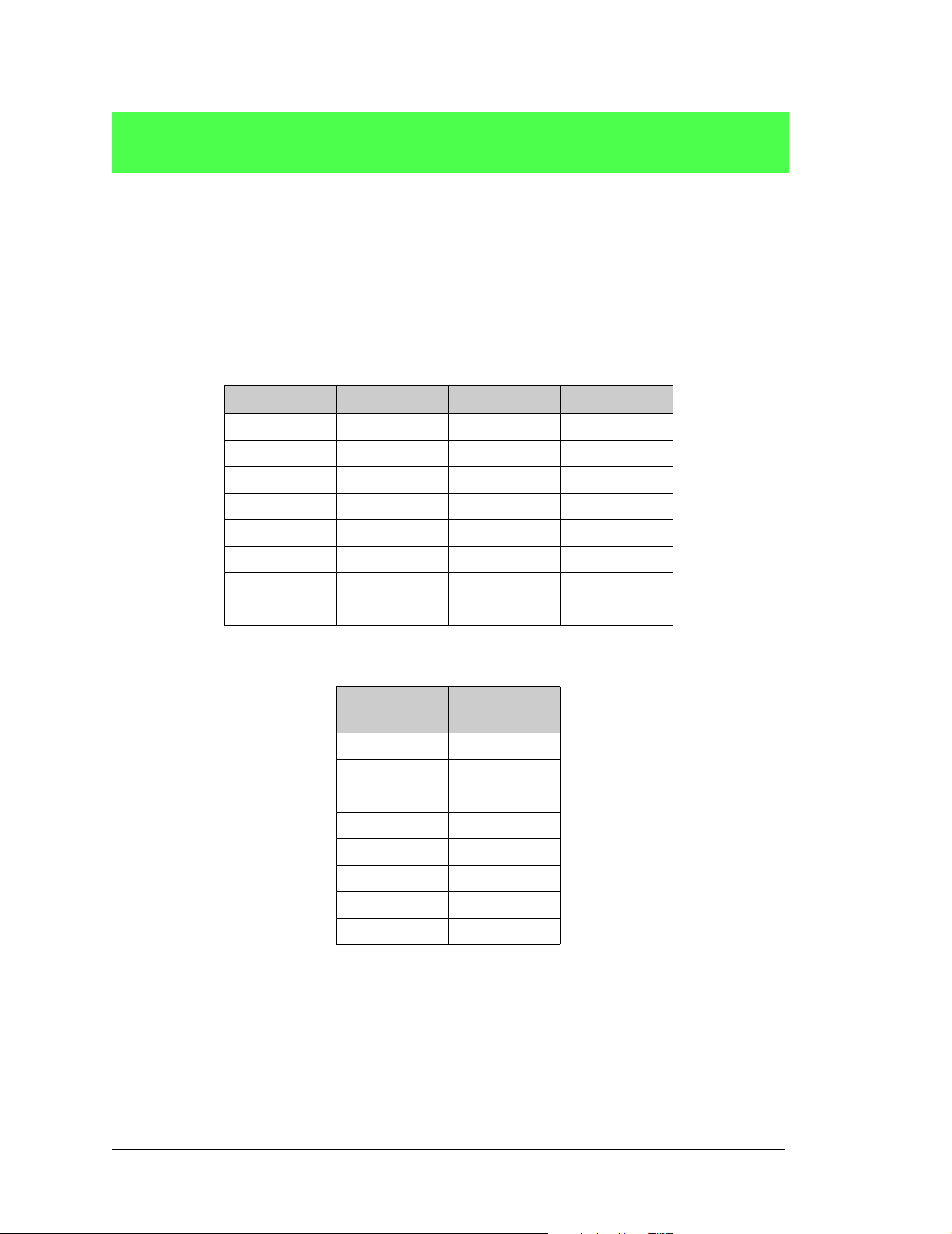
int anaIn(unsigned int channel, int opmode,
int gaincode);
Reads the value of an analog input channel using the direct method of addressing the ADS7870 A/D
converter.
PARAMETERS
channel is the analog input channel number (0 to 7) corresponding to AIN0–AIN7
opmode is the mode of operation:
SINGLE—single-ended input line
DIFF—differential input li ne
mAMP—milliamp input line
channel SINGLE DIFF mAMP
0 +AIN0 +AIN0 -AIN1 +AIN0
1 +AIN1 — +AIN1
2 +AIN2 +AIN2 -AIN3 +AIN2
3 +AIN3 — +AIN3
4 +AIN4 +AIN4 -AIN5 —
5 +AIN5 — —
6 +AIN6 +AIN6 -AIN7 —
7 +AIN7 — —
gaincode is the gain code of 0 to 7:
Gain Code
0 0–20 V
1 0–10 V
20–5 V
30–4 V
4 0–2.5 V
50–2 V
60–1.25 V
70–1 V
RETURN VALUE
A value corresponding to the voltage on the analog input channel, which will be:
0–2047 for 11-bit A/D conversions (signed 12th bit)
ADOVERFLOW (defined macro = -4096) if overflow or out of range
SEE ALSO
anaIn, anaInConfig, anaInDriver
Voltage
Range
56 Fox (LP3500)
Page 63
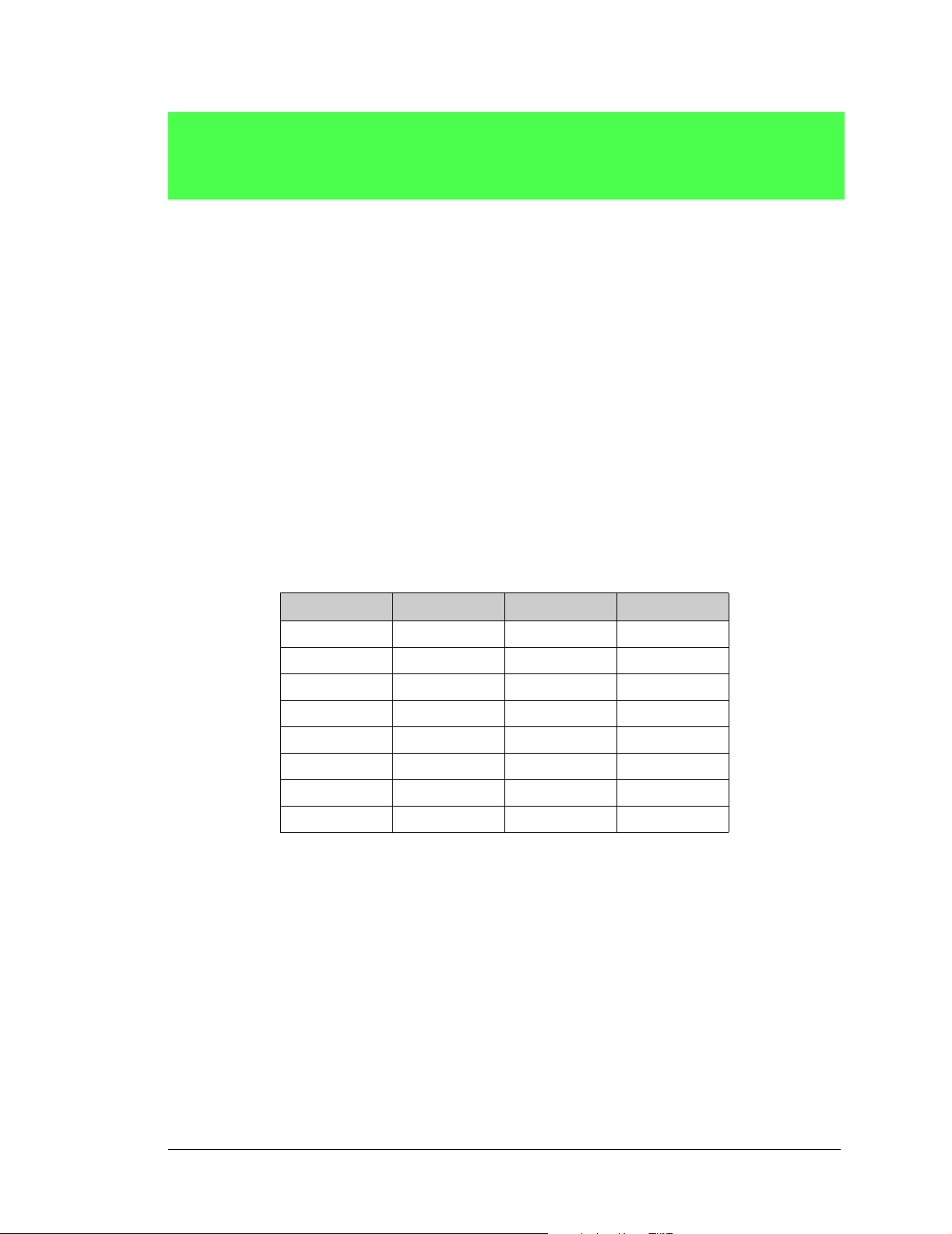
int anaInCalib(int channel, int opmode,
int gaincode, int value1, float volts1,
int value2, float volts2);
Calibrates the response of the A/D converter channel as a linear function using the two conversi on poi nts
provided. Four values are calculated and placed into global table _adcCalib to be stored later store
into simulated EEPROM using the function anaInEEWr(). Each channel will have the following
information:
a linear constant,
a voltage offset,
a calculation gain code used to calculate calibrations, and
a user gain code to set voltage range (defaults to the calculation gain code).
NOTE: Vcc monitoring is disabled when anaInCalib is running.
PARAMETERS
channel is the analog input channel number (0 to 7) corresponding to AIN0–AIN7
opmode is the mode of operation:
SINGLE—single-ended input line
DIFF—differential input li ne
mAMP—milliamp input line
channel SINGLE DIFF mAMP
0 +AIN0 +AIN0 -AIN1 +AIN0
1 +AIN1 — +AIN1
2 +AIN2 +AIN2 -AIN3 +AIN2
3 +AIN3 — +AIN3
4 +AIN4 +AIN4 -AIN5 —
5+AIN5— —
6 +AIN6 +AIN6 -AIN7 —
7+AIN7— —
User’s Manual 57
Page 64
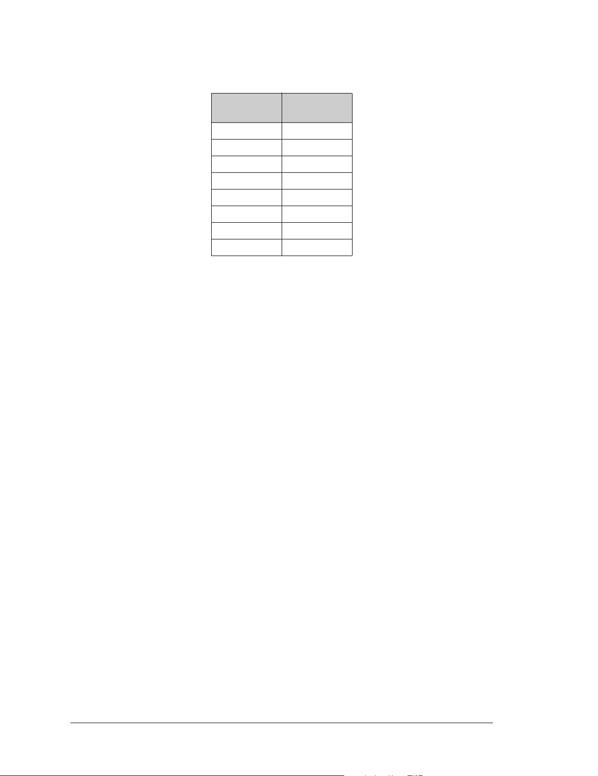
gaincode is the gain code of 0 to 7:
Gain Code
Voltage
Range
0 0–20 V
1 0–10 V
20–5 V
30–4 V
4 0–2.5 V
50–2 V
60–1.25 V
70–1 V
value1 is the first A/D converter channel value (0–2047).
volts1 is the voltage or current corresponding to the first A/D converter channel value (0 to +10 V or
4to 20 mA).
value2 is the second A/D converter channel value (0–2047).
volts2 is the voltage or current corresponding to the first A/D converter channel value (0 to +10 V or
4to 20 mA).
RETURN VALUE
0 if successful.
-1 if not able to make calibration constants.
SEE ALSO
anaIn, anaInVolts, anaInmAmps, anaInDiff, anaInSetRange, anaInVoltXGain,
anaInCalib, brdInit
58 Fox (LP3500)
Page 65
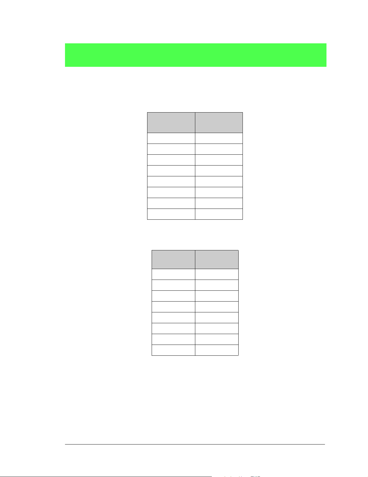
float anaInVolts(unsigned int channel, unsigned int
gaincode);
Reads the state of a single-ended analog in put channel and uses the previously set calibration constants to
convert it to volts.
PARAMETER
channel is the channel number (0–7):
Channel Code
* Negative input is ground.
gaincode is the gain code of 0 to 7.
Gain Code
Single-Ended
Input Lines
0+AIN0
1+AIN1
2+AIN2
3+AIN3
4+AIN4
5+AIN5
6+AIN6
7+AIN7
Voltage
Range
0 0–20 V
1 0–10 V
*
20–5 V
30–4 V
4 0–2.5 V
50–2 V
60–1.25 V
70–1 V
RETURN VALUE
A voltage value corresponding to the voltage on the analog input channel.
ADOVERFLOW (defined macro = -4096) if overflow or out of range.
SEE ALSO
anaInCalib, anaIn, anaInmAmps, brdInit
User’s Manual 59
Page 66
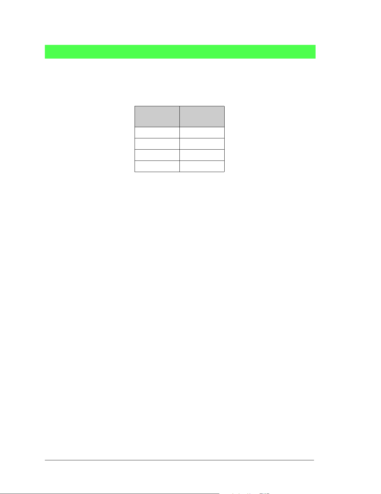
int anaInmAmps(unsigned int channel);
Reads the state of an analog input channel and uses the previous ly se t calibration constants to convert it
to current.
PARAMETER
channel is 0–3:
Channel
4–20 mA
Input Lines
*
0AIN0
1AIN1
2AIN2
3AIN3
* Negative input is ground.
RETURN VALUE
A current value between 4.00 and 20.00 mA corresponding to the current on the analog input channel.
ADOVERFLOW (defined macro = -4096) if overflow or out of range.
SEE ALSO
anaInCalib, anaIn, anaInVolts
60 Fox (LP3500)
Page 67
float anaInDiff(unsigned int channel, unsigned int
gaincode);
Reads the state of a differential analog input channel and uses the previously set calibration constants to
convert it to volts.
PARAMETER
channel is the channel number (0, 2, 4, 6):
Channel
gaincode is the gain code of 0 to 7.
Gain Code
Differential
Input Lines
0 +AIN0 -AIN1
2 +AIN2 -AIN3
4 +AIN4 -AIN5
6 +AIN6 -AIN7
Voltage
Range
0 0–20 V
1 0–10 V
20–5 V
30–4 V
4 0–2.5 V
50–2 V
60–1.25 V
70–1 V
RETURN VALUE
A voltage value corresponding to the voltage on the analog input channel.
ADOVERFLOW (defined macro = -4096) if overflow or out of range.
SEE ALSO
anaInCalib, anaIn, anaInmAmps, brdInit
User’s Manual 61
Page 68
int anaInEERd(unsigned int channel, int opmode,
unsigned int gaincode);
Reads the calibration constants, gain, and offset for an input based on its designated channel code position into global table _adcCalib. The constants are stored in the the top 1K of the reserved user block
memory area 0x1C00–0x1FFF.
NOTE: This function cannot be run in RAM.
PARAMETER
channel is the analog input channel number (0 to 7) corresponding to AIN0–AIN7.
opmode is the mode of operation:
SINGLE—single-ended input line
DIFF—differential input li ne
mAMP—milliamp input line
channel SINGLE DIFF mAMP
0 +AIN0 +AIN0 -AIN1 +AIN0
1 +AIN1 — +AIN1
2 +AIN2 +AIN2 -AIN3 +AIN2
3 +AIN3 — +AIN3
4 +AIN4 +AIN4 -AIN5 —
5 +AIN5 — —
6 +AIN6 +AIN6 -AIN7 —
7 +AIN7 — —
ALLCHAN read all channels for selected opmode
gaincode is the gain code of 0 to 7. The gaincode parameter is ign ored when channel is ALLCHAN.
Gain Code
0 0–20 V
1 0–10 V
20–5 V
30–4 V
4 0–2.5 V
50–2 V
60–1.25 V
70–1 V
RETURN VALUE
0 if successful.
-1 if address is invalid or out of range.
SEE ALSO
anaInEEWr, anaInCalib
62 Fox (LP3500)
Voltage
Range
Page 69
int anaInEEWr(unsigned int channel, int opmode
unsigned int gaincode);
Writes the calibration constants, gain, and offset for an input based on its designated channel code position from global table _adcCalib. The constants are stored in the the top 1K of the reserved u ser block
memory area 0x1C00–0x1FFF.
NOTE: This function cannot be run in RAM.
PARAMETER
channel is the analog input channel number (0 to 7) corresponding to AIN0–AIN7.
opmode is the mode of operation:
SINGLE—single-ended input line
DIFF—differential input li ne
mAMP—milliamp input line
channel SINGLE DIFF mAMP
0 +AIN0 +AIN0 -AIN1 +AIN0
1 +AIN1 — +AIN1
2 +AIN2 +AIN2 -AIN3 +AIN2
3 +AIN3 — +AIN3
4 +AIN4 +AIN4 -AIN5 —
5+AIN5— —
6 +AIN6 +AIN6 -AIN7 —
7+AIN7— —
ALLCHAN read all channels for selected opmode
gaincode is the gain code of 0 to 7. The gaincode parameter is ign ored when channel is ALLCHAN.
Gain Code
0 0–20 V
1 0–10 V
20–5 V
30–4 V
4 0–2.5 V
50–2 V
60–1.25 V
70–1 V
RETURN VALUE
0 if successful.
-1 if address is invalid or out of range.
SEE ALSO
anaInEEWr, anaInCalib
User’s Manual 63
Voltage
Range
Page 70

4.5.6 Vcc Monitoring (LP3500 only)
void VccMonitorInit(int state);
PIO3 on the ADS7870 A/D converter enables or disables Vcc monitoring. If monitoring is enabled, analog input channel AIN7 is not available.
PARAMETER
state
1 = enable Vcc monitor
0 = disable Vcc monitor
SEE ALSO
VccMonitor, anaInConfig, brdInit
float VccMonitor(void);
If Vcc monitoring is enabled, the Vcc level is read by the ADS7870 A/D converter and is converted to a
voltage value.
RETURN VALUE
A voltage value corresponding to the voltage on the analog input channel.
SEE ALSO
VccMonitorInit, anaInVolts, brdInit
64 Fox (LP3500)
Page 71

4.5.7 PWM Outp uts
The PWM functions in this section can be used to operate the analog outputs on the
LP3500 model.
int pwmOutConfig(unsigned long frequency);
Sets the base frequency for the PWM pulses and enables the PWM driver on all four channels. The base
frequency is the frequency without pulse spreading. Pulse spreading (see pwm_set) will increase the
frequency by a factor of 4.
PARAMETERS
frequency is the frequency (in Hz).
RETURN VALUE
Actual frequency set. This will be the closest possible match to the requested frequency.
SEE ALSO
pwmOut
int pwmOut(unsigned int channel, float dutycycle);
Sets a voltage (0 to VDD on an analog output channel according to the percent duty cycle of the 1024clock-count cycle.)
PARAMETERS
channel is the output channel to write to (0–3).
dutycycle is the percent duty (or on) cycle value of the 1024-clock-count cycle (i.e., 0.25).
RETURN VALUE
0 if successful
-1 if an invalid channel number is used
-2 if an invalid duty cycle was requested
SEE ALSO
pwmOutConfig
User’s Manual 65
Page 72

4.6 Relay Output (LP3500 only)
int relayOut(int relay, int value)
A 10 ms low-to-high pulse sets the state of a relay. On power-up or brdInit() the relay contact will
go to the normally closed (NC) RESET contact.
PARAMETERS
relay
0 = the one relay
value is a value used to connect the relay common contact:
0 = relay normally closed (NC or RESET) (Parallel Port PG5)
1 = relay normally open (NO or SET) (Parallel Port PG4)
RETURN VALUE
0 if successful
-1 if the normal power source is not available
66 Fox (LP3500)
Page 73

APPENDIX A. LP3500 SPECIFICATIONS
Appendix A provides the specifications for the LP3500, and
describes the conformal coating.
User’s Manual 67
Page 74
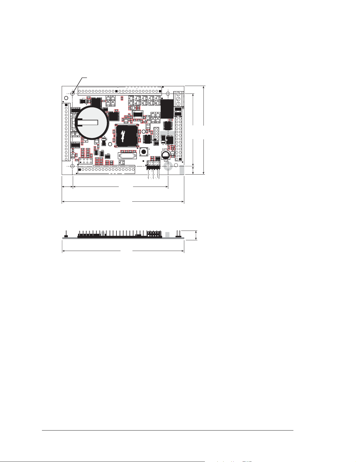
A.1 Electrical and Mechanical Characteristics
Figure A-1 shows the mechanical dimensions for the LP3500.
0.120 dia
J4
J1
IN00 IN01 IN02 IN03 IN04 IN05 IN06 IN07 GND IN08 IN09 IN10 IN11 IN12 IN13 IN14 IN15
RN2
C15
C12
D5
D11
D7
C6
D4
D2
C8
D8
C10 C13
C2
RN1
C3
R6
R17
R7
R9
D1
R1
AIN0 AIN1 AIN2 AIN3
AIN0 AIN1 AIN2 AIN3 AIN4 AIN5 AIN6 AIN7 GND GND
(3.05)
D19
C16
U1
C36
C19
C20
R13
R16
D18
D15 D17
RP17
R57
Battery
R31
C22
C29
BT1
D13
R23
Q22
R30
C24
R18
C26
C33
R29
R20
R25
J3
C37
R26
R22
OUT9
OUT8
OUT7
+K GND 485 + GND TxB RxB GND TxC RxC GND TxE RxE GND
D20
D21
C48
U3
C43
C44
Y1
R32
C40
PWM1
PWM2
PWM0
D26
R37
D25
Q8
Q5
R42
R38
Q6
C53
C51
R34
R41
R39
C55
U8
R40 C54
R36
C50
D22
VBAT
GND VIN GND
EXT
OUT1
OUT0
OUT2
OUT5
OUT4
OUT3
OUT6
D28
Q10
R43
R33
Y2
R44
R45
C59
C60
U9
S1
RESET
J2
GND
J8
RELAY
D30
D34
Q17
Q16
K1
Q13
D32
C61
Q12
R47
R48
U10
R50
R49
J5
U11
RP13
PROGRAM
C67
U12
D33Q14
J6
C66
C64
U13
R51
C65
RP14
PORT
NC
COM
NO
R56
R55
J9
C70
R58
Q20
R54
GND
(54)
(66)
2.11
DISPLAY
2.60
Please refer to the LP3500
footprint diagram later in this
appendix for precise header
locations.
0.29
(7.4)
2.84
(72)
3.65
(93)
3.65
(93)
(6.0)
0.245
0.45
(11)
Figure A-1. LP3500 Dimensions
68 Fox (LP3500)
Page 75
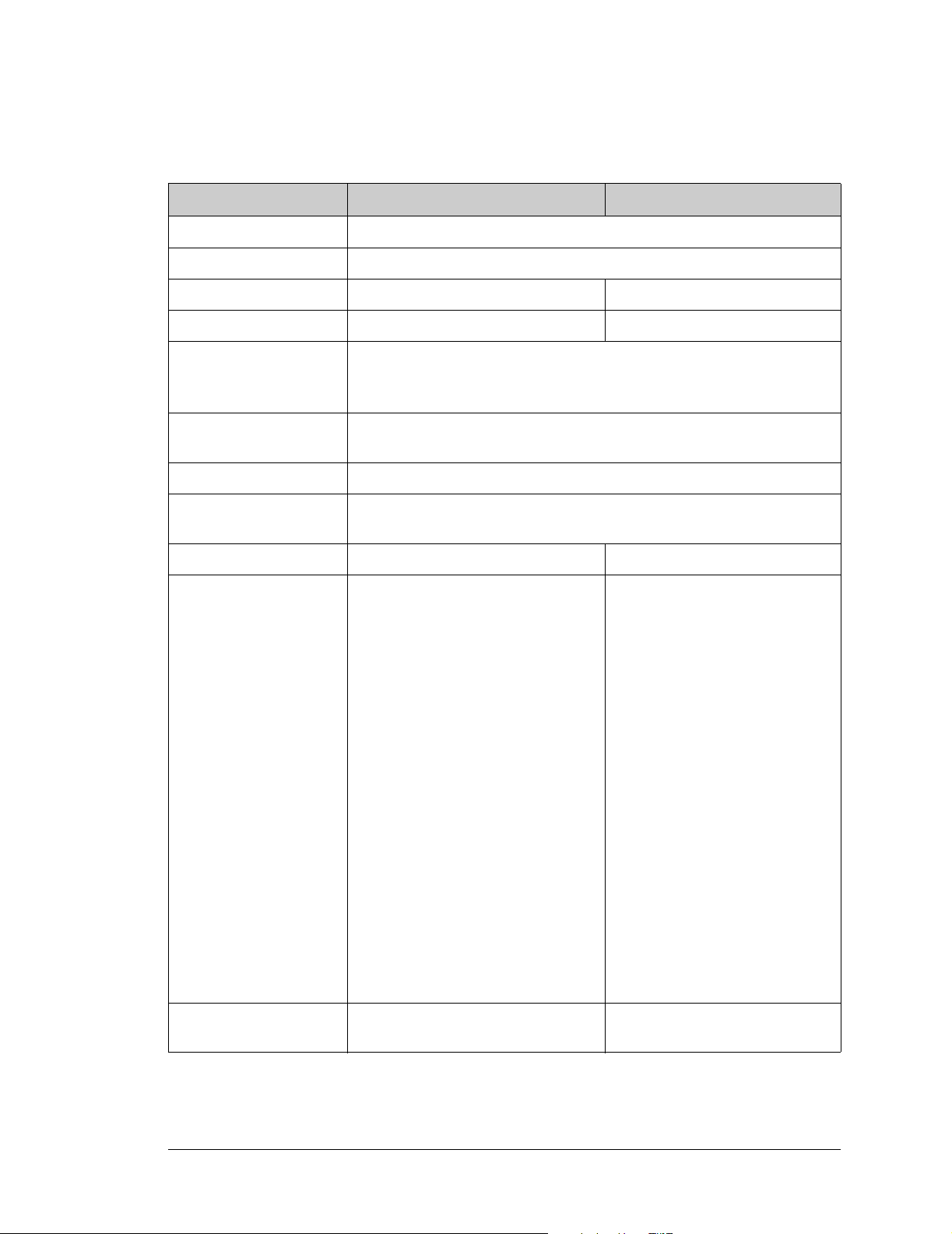
T ableA-1 lists the electrical, mechanical, and environmental specifications for the LP3500.
Table A-1. LP3500 Specifications
Feature LP3500 LP3510
Microprocessor Rabbit 3000® at up to 7.4 MHz
EMI Reduction Spectrum spreader for ultra-low EMI (radiated emissions)
Flash Memory 512K (2 × 256K) 256K
SRAM 512K 128K
Socketed 3 V lithium coin
Backup Battery
connection for user-supplied external battery
Keypad/Display
Digital Inputs 16: fully protected 0–36 V DC, can handle short spikes ±40 V
Digital Outputs
Relay Output 1 C-form, 1 A, 30 V DC None
10: 8 sink up to 200 mA each, 36 V DC max.;
2 source up to 200 mA each, 36 V DC max.
Supports optional LCD/keypad module with
supports RTC and SRAM,
7 keys and 122 × 32 graphic display
Panasonic CR2330, 265 mA·h,
• Eight single-ended or four
differential inputs
• 1MΩ input impedance
• Sampling rate up to 200 samples/s
• Eight software-controlled ranges
from 0–1 V to 0–20 V DC
Single-Ended Inputs
• Resolution: 11 bits
Analog Inputs
None
• Accuracy: 8 bits
• 4 channels can be set individual ly for
4–20 mA with plug-in jumpers
• 1 channel has software-selectable
voltage-monitoring option
Differential Inputs
• Resolution: 12 bits
• Accuracy: 9 bits
Analog Outputs
User’s Manual 69
3 unfiltered pulse-width modulated,
1 kΩ output impedance
None
Page 76
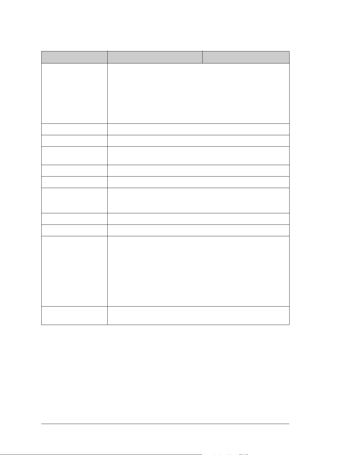
Table A-1. LP3500 Specifications (continued)
Feature LP3500 LP3510
6 shared high-speed, CMOS-compatible ports:
• 1 RS-485
Serial P orts
logic-level outputs; one RS-232 port needs to have wake-up capability
• 1 logic-level serial interface for optional add-ons
• 1 asynchronous clocked serial port dedicated for pro gramm in g
• 3 RS-232 (one 5-wire and one 3-wire or three 3-wire), jumper option for
Serial Rate Max. asynchronous baud rate = CLK/8
Real-Time Clock Yes
Timers
W atchdog/Supervisor Yes
Pulse-Width Modulators 10-bit free-running counter and four pulse-width registers
Power
Operating T emperatu re –40°C to +70°C
Humidity 5% to 95%, noncondensing
Ten 8-bit timers (6 cascadable from the first),
one 10-bit timer with 2 match registers
3 V to 30 V DC
20 mA (max.) @ 7.4 MHz,
100 µA max. @ 2 kHz (with linear regulator turned off)
• 0.1" headers
I/O and misc. signals: one 1 × 25, two 1 × 17 headers
Display: one 2 × 13 header
Connectors
• 2 mm headers
Programming Port: one 2 × 5 header
Serial Interface: one 2 × 4 socket
• Screw-terminal headers
Relay: one 3-position screw-terminal header
Board Size
70 Fox (LP3500)
2.60" × 3.65" × 0.45"
(66 mm × 93 mm × 11 mm)
Page 77
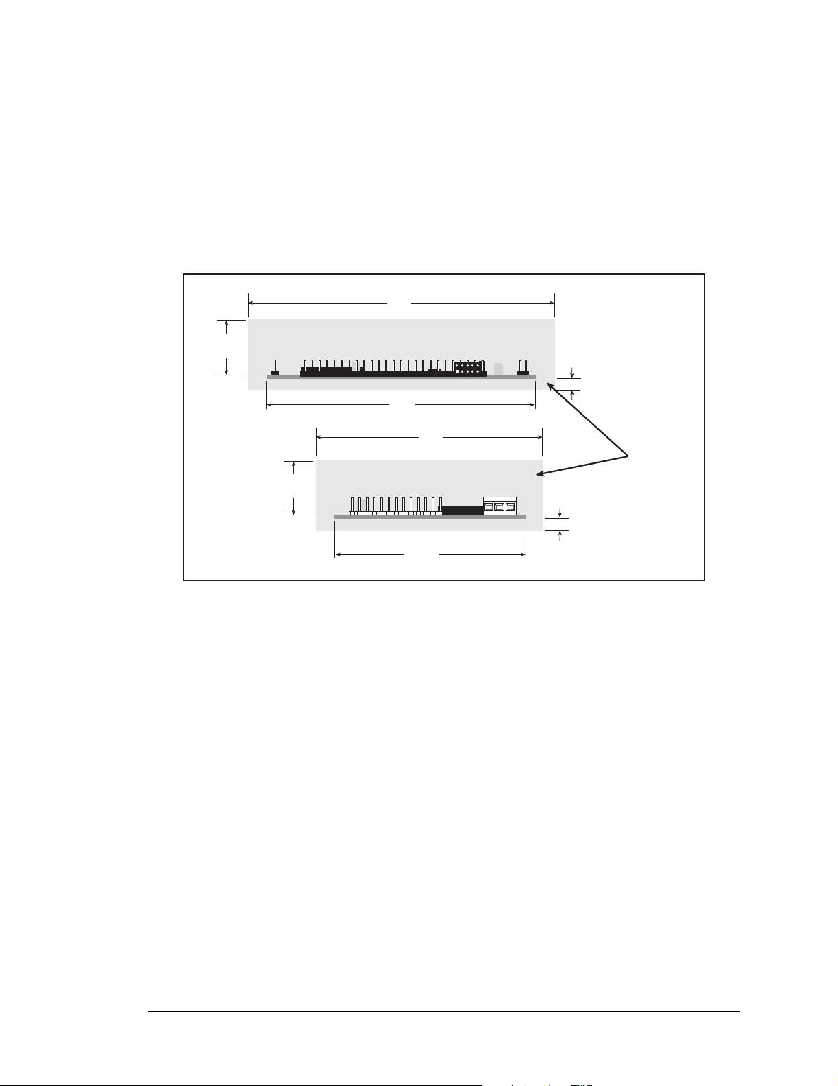
A.1.1 Exclusion Zone
It is recommended that you allow for an “exclusion zone” of 0.25" (6 mm) around the
LP3500 in all directions when the LP3500 is incorporated into an assembly that includes
other printed circuit boards. This “exclusion zone” that you keep free of other components
and boards will allow for sufficient air flow, and will help to minimize any electrical or
electromagnetic interference between adjacent boards. An “exclusion zone” of 0.12"
(3 mm) is recommended below the LP3500. Figure A-2 shows this “exclusion zone.”
4.15
(105)
(18)
0.70
0.70
(18)
3.65
(93)
3.10
(79)
0.12
(3)
0.12
(3)
Exclusion
Zone
2.60
(66)
Figure A-2. LP3500 “Exclusion Zone”
When using the LP3500 with the Prototyping Board, do not install any components in the
prototyping area on the Prototyping Board between the LP3500 and the Prototyping
Board.
User’s Manual 71
Page 78
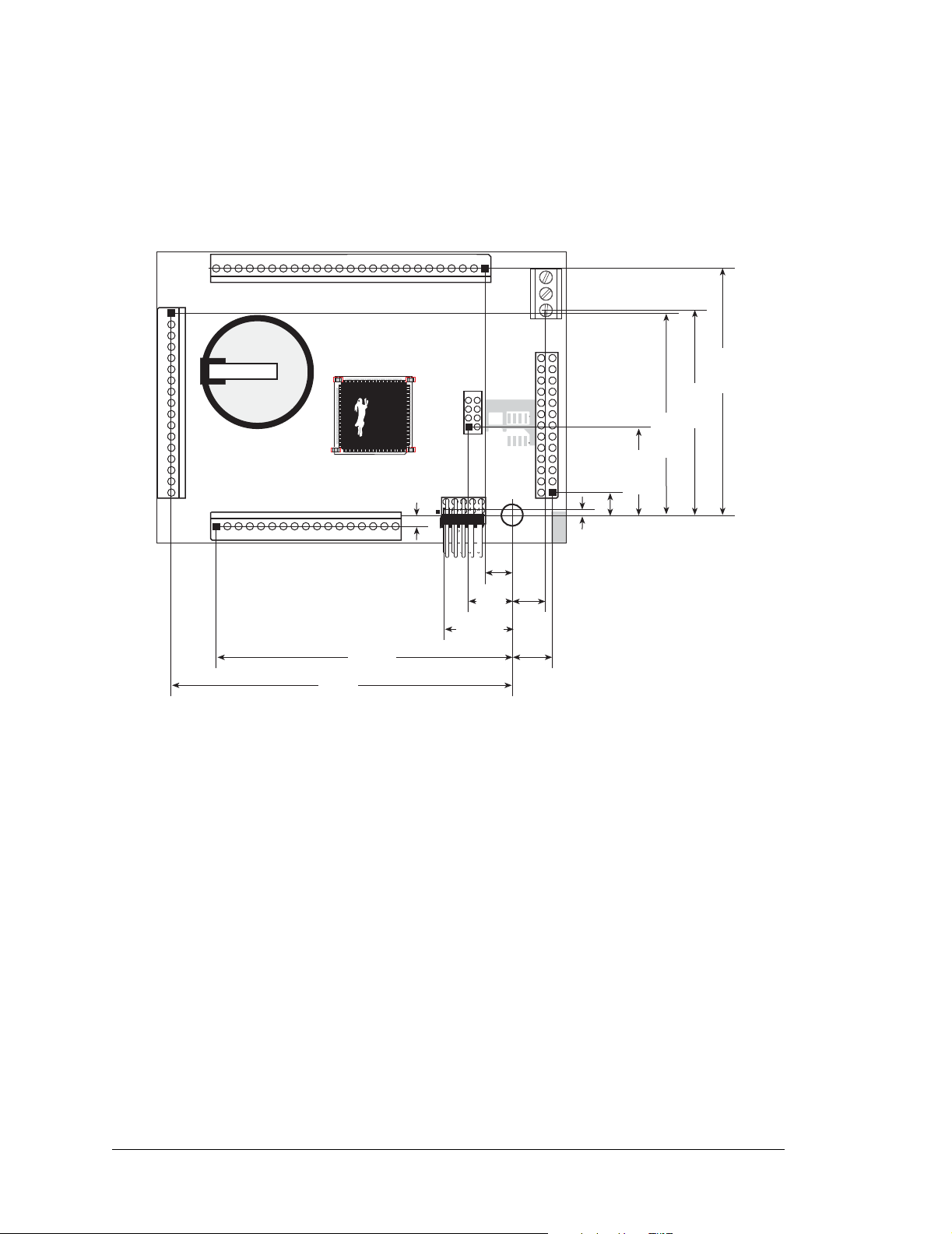
A.1.2 Headers
The LP3500 uses 0.1" IDC headers at J1–J4 for physical connection to other boards. J5,
the programming port, is a 2 × 5 header with a 2 mm pin spacing.
Figure A-3 shows the LP3500 footprint. These values are relative to the mounting hole.
J1
J2
3.040
(77.2)
2.640
(67.1)
0.100
(2.54)
J6
J5
J4
PROGRAM
PORT
0.590
(15.0)
0.390
(9.9)
J8
J9
0.240
(6.1)
0.320
(8.1)
0.360
(9.1)
(1.0)
0.040
(5.1)
0.200
1.800
(20.0)
0.787
1.820
(45.7)
2.200
(46.2)
(55.9)
Figure A-3. User Board Footprint for LP3500
72 Fox (LP3500)
Page 79
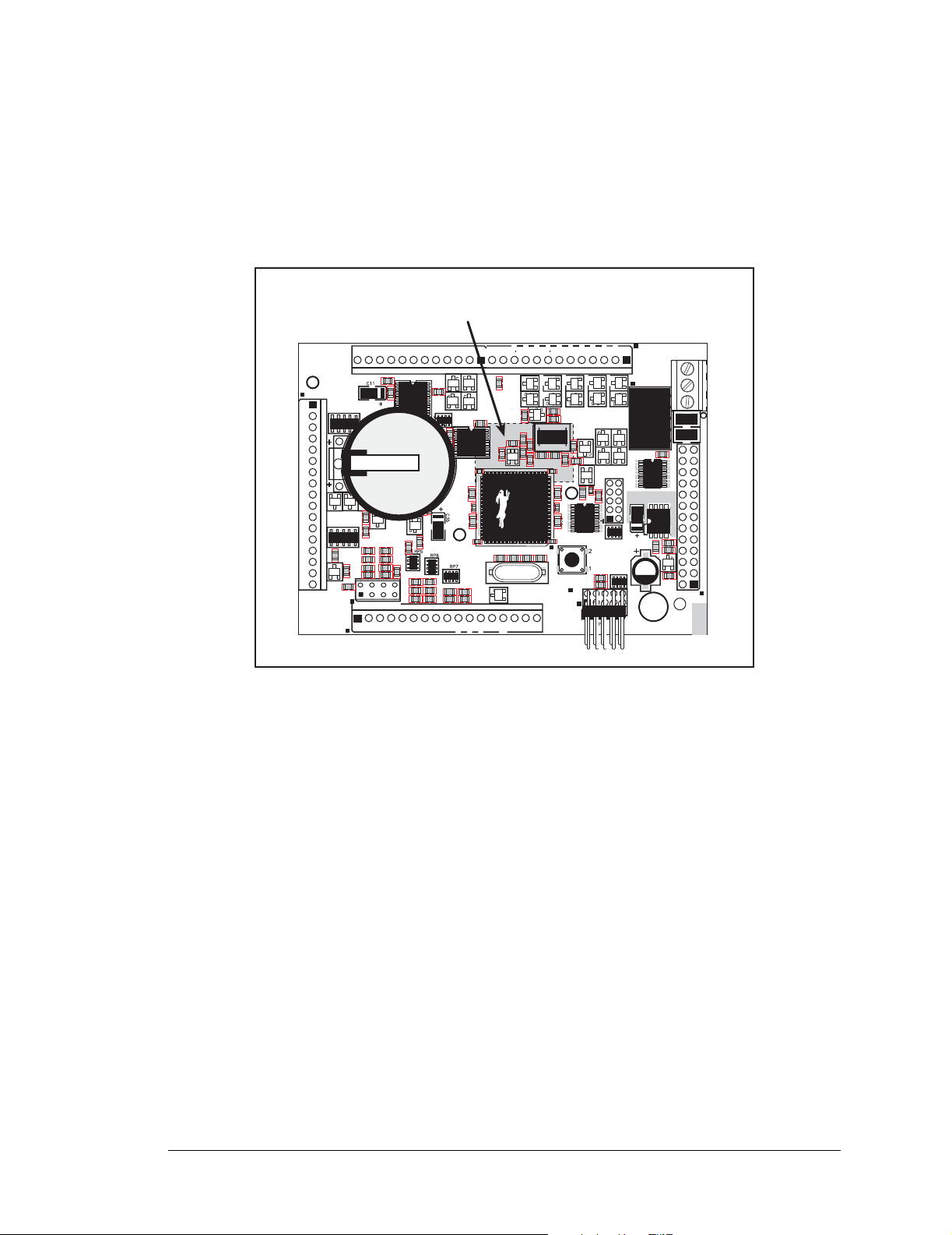
A.2 Conformal Coating
The areas around the 32 kHz real-time clock crystal oscillator has had the Dow Corning
silicone-based 1-2620 conformal coating applied. The conformally coated area is shown
in Figure A-4. The conformal coating protects these high-impedance circuits from the
effects of moisture and contaminants over time.
Conformally
coated area
OUT1
RESET
OUT0
OUT2
OUT4
OUT3
Q10
Y2
C61
Q12
R47
U10
S1
R50
R49
J5
D30
R48
Q16
Q13
U11
C66
RP13
PROGRAM
PORT
GND
J8
RELAY
D34
Q17
K1
D32
C67
U12
D33Q14
J6
C64
U13
C70
R51
C65
Q20
RP14
NC
COM
NO
R56
R55
J9
DISPLAY
R58
R54
GND
J1
IN00 IN01 IN02 IN03 IN04 IN05 IN06 IN07 GND IN08 IN09 IN10 IN11 IN12 IN13 IN14 IN15
D2
D1
J4
Q22
D13
C24
R18
J3
U1
D15 D17
C22
R23
R30
C26
R20
R22
D19
C36
RP17
R57
Battery
R31
C29
BT1
C33
R29
R25
C37
R26
D18
C16
RN2
C19
C15
C12
C20
D5
D11
D7
C6
D4
C8
D8
C10 C13
C2
RN1
R13
C3
R6
R16
R17
R7
R9
R1
AIN0 AIN1 AIN2 AIN3
AIN0 AIN1 AIN2 AIN3 AIN4 AIN5 AIN6 AIN7 GND GND
OUT9
OUT8
OUT5
OUT7
OUT6
+K GND 485 + GND TxB RxB GND TxC RxC GND TxE RxE GND
R42
R38
Q6
R39
R40 C54
D28
D26
Q8
R43
R33
C53
R41
R44
C55
R45
C59
C60
U9
J2
D20
R37
D25
Q5
D21
C48
C51
R34
U3
U8
C43
C44
R36
C50
Y1
R32
C40
D22
PWM1
PWM2
PWM0
VBAT
GND VIN GND
EXT
Figure A-4. LP3500 Areas Receiving Conformal Coating
Any components in the conformally coated area may be replaced using standard soldering
procedures for surface-mounted components. A new conformal coating should then be
applied to offer continuing protection against the effects of moisture and contaminants.
NOTE: For more information on conformal coatings, refer to Technical Note 303, Con-
formal Coatings.
User’s Manual 73
Page 80
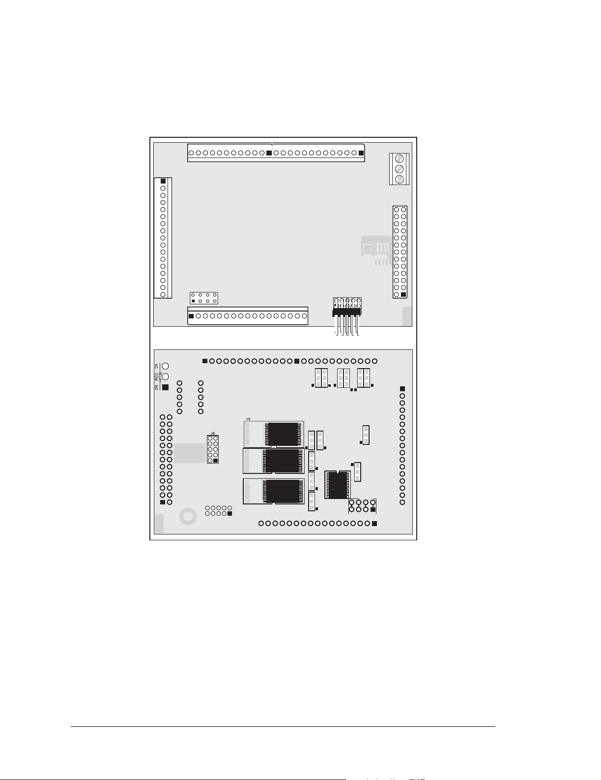
A.3 Jumper Configurations
Figure A-5 shows the header locations used to configure the various LP3500 options via
jumpers.
Top Side
J3
JP6
JP11
JP4
JP5
CTS RTS
JP3
JP2
JP1
GND
OUT0
OUT1
OUT2
OUT3
Bottom Side
OUT8
OUT9
GND +KGND RxE TxE GND RxC TxC GND RxB TxB GND + 485
OUT4
OUT5
OUT6
OUT7
JP7
JP12
JP8
U6
U2
JP13
JP9
420 mA
AIN3
AIN2
AIN1
AIN0
AIN6
AIN5
AIN4
AIN3
AIN2
AIN1
AIN0
PROGRAM
PORT
U7
VBAT
VIN
EXT
GND
GND
GND
JP10
GND
AIN7
PWM2
PWM1
PWM0
Figure A-5. Location of LP3500 Configurable Positions
IN00
IN01
IN02
IN03
IN04
IN05
IN06
IN07
GND
IN08
IN09
IN10
IN11
IN12
IN13
IN14
IN15
74 Fox (LP3500)
Page 81
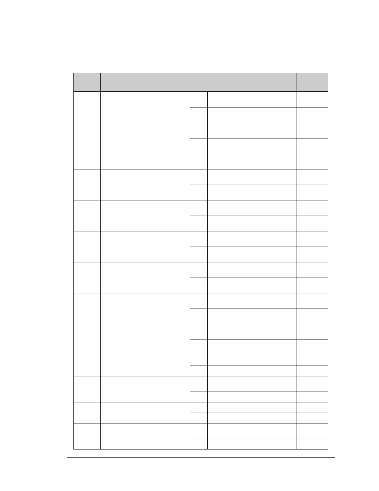
Table A-2 lists the configuration options.
Table A-2. LP3500 Jumper Configurations
Header Description Pins Connected
None Voltage Option
1–2 AIN0 4–20 mA Option
A/D Converter Voltage/Current
J3
Measurement Options
JP1 RxE RS-232/Logic Level Select
JP2 TxE RS-232/Logic Level Select
JP3 RxC RS-232/Logic Level Select
3–4 AIN1 4–20 mA Option
5–6 AIN2 4–20 mA Option
7–8 AIN3 4–20 mA Option
1–2 RS-232 Level
2–3 Logic Level
1–2 RS-232 Level
2–3 Logic Level
1–2 RS-232 Level
2–3 Logic Level
Factory
Default
×
×
×
×
JP4 TxC RS-232/Logic Level Select
JP5 RxB RS-232/Logic Level Select
JP6 TxB RS-232/Logic Level Select
JP7 SRAM Size
JP8 Flash Memory Size
JP9 Flash Memory Size
JP10 Flash Memory Bank Select
1–2 RS-232 Level
2–3 Logic Level
1–2 RS-232 Level
2–3 Logic Level
1–2 RS-232 Level
2–3 Logic Level
1–2 128K LP3510
2–3 512K LP3500
1–2 128K/256K
2–3 512K
1–2 128K/256K LP3500
2–3 512K
1–2 Normal Mode
2–3 Bank Mode
×
×
×
×
×
User’s Manual 75
Page 82
Table A-2. LP3500 Jumper Configurations (continued)
Header Description Pins Connected
JP11 Manufacturing Use 1–2
JP12 M anufacturing Use 1–2
JP13 M anufacturing Use 1–2
NOTE: The jumper connections on header J3 are made using standard slip-on jumpers.
All other jumper connections except those across JP11 and JP12 are made using 0 Ω
surface-mounted resistors. 390 Ω current-limiting resistors are used on JP11 and JP12.
Factory
Default
×
×
×
76 Fox (LP3500)
Page 83
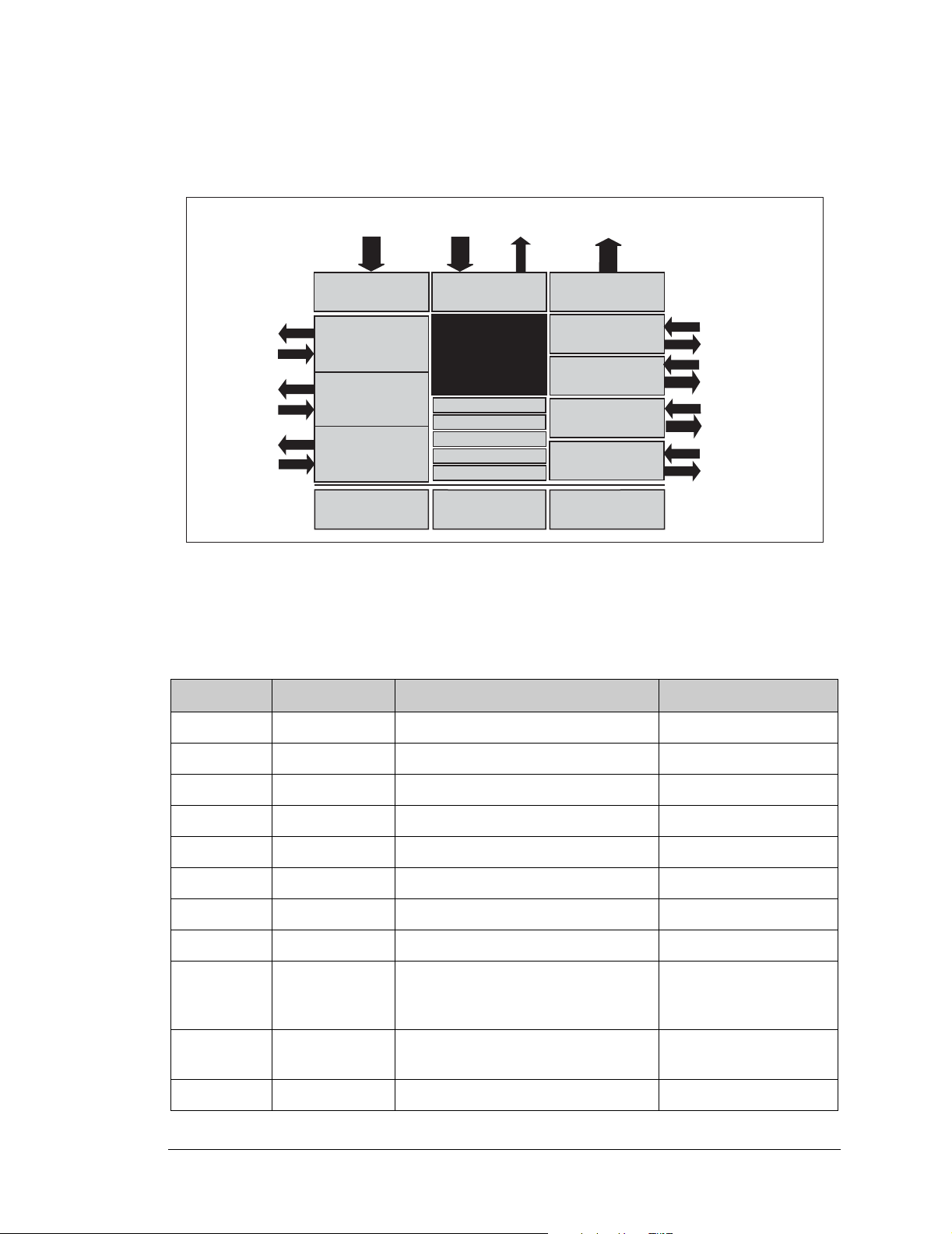
A.4 Use of Rabbit 3000 Parallel Ports
Figure A-6 shows the Rabbit 3000 parallel ports.
PD0PD7
Port D
Port E
Port F
Port G
(+Serial Ports)
Misc. I/O
Flash
PE0PE1, PE4PE5
PE2PE3, PE6PE7
PF1PF2
PF0, PF3PF7
PG3, PG7
PG0PG2, PG4PG6
/RES_IN
/IORD
/RESET,
/IOWR,
STATUS
SMODE0
SMODE1
PC0, PC2, PC4
PC1, PC3, PC5
PG2, PG6
PG3, PG7
PC6
PB1, PC7, /RES
PA0PA7
Port A
Port C
(Serial Ports B,C & D)
Port G
(Serial Ports E & F)
Programming
Port
(Serial Port A)
RAM
PB0PB5
PB6PB7
Port B
R
ABBIT
3000
Real-Time Clock
Watchdog
11 Timers
Slave Port
Clock Doubler
Backup Battery
Support
Figure A-6. LP3500 Rabbit-Based Subsystems
Table A-3 lists the Rabbit 3000 parallel ports and their use in the LP3500.
Table A-3. Use of Rabbit 3000 Parallel Port s
Port I/O Signal Output Function State
PA0 Input IN08
PA1 Input IN09
PA2 Input IN10
PA3 Input IN11
PA4 Input IN12
PA5 Input IN12
PA6 Input IN14
PA7 Input IN15
Pulled up
Pulled up
Pulled up
Pulled up
Pulled up
Pulled up
Pulled up
Pulled up
Low when external power
PB0 Input Power Input Detect
source is connected; high
for battery
PB1 Input CLKA
PB2 Input IN04
Pulled up when not driven
by programming port
Pulled up
User’s Manual 77
Page 84
Table A-3. Use of Rabbit 3000 Parallel Ports (continued)
Port I/O Signal Output Function State
PB3 Input IN05
PB4 Input IN06
PB5 Input IN07
Pulled up
Pulled up
Pulled up
PB6 Output LCD Buffer Enable Inactive high
PB7 Output Serial Device Select Inactive high
PC0 Output TXD Serial Device Int.
Inactive high
Serial Port D
PC1 Input RXD Serial Device Int. Inactive high
PC2 Output RTS/TxC RS-232
Inactive high
Serial Port C
PC3 Input CTS/RxC RS-232 Inactive high
PC4 Output TxB RS-232
Inactive high
Serial Port B
PC5 Input RxB RS-232 Inactive high
PC6 Output TxA Programming Port
Inactive high
Serial Port A
PC7 Input RxA Programming Port Inactive high
PD0 Output OUT0 Inactive low
PD1 Output OUT1 Inactive low
PD2 Output OUT2 Inactive low
PD3 Output OUT3 Inactive low
PD4 Output OUT4 Inactive low
PD5 Output OUT5 Inactive low
PD6 Output OUT6 Inactive low
PD7 Output OUT7 Inactive low
PE0 Input IN00
Pulled up
PE1 Input IN01 Pulled up
PE2 Output OUT8 Inactive low
PE3 Output OUT9 Inactive low
PE4 Input IN02
Pulled up
PE5 Input IN03 Pulled up
PE6 Output LCD/Keypad Module Reset Line Inactive high
PE7 Output LCD/Keypad Module Device Select Inactive high
78 Fox (LP3500)
Page 85
Table A-3. Use of Rabbit 3000 Parallel Ports (continued)
Port I/O Signal Output Function State
PF0 Output ADC Serial Clock Inactive high
PF1 Input ADC Busy Inactive low
PF2 Input Not used Pulled up
PF3 Output ADC Device Select Inactive high
PF4 Output PWM0 Inactive high
PF5 Output PWM1 Inactive high
PF6 Output PWM2 Inactive high
Low when external power
PF7 Output Powe r Enable Control
PG0 Output RS-485 Transmit Enable Inactive low
PG1 Output RS-232 Shutdown Control Inactive high
source is connected; high
for battery
PG2 Output TxF RS-485
Inactive high
Serial Port F
PG3 Input RxF RS-485 Inactive high
PG4 Output Relay Set Inactive low
PG5 Output Relay Reset Inactive low
PG6 Output TxE RS-232
Inactive high
Serial Port E
PG7 Input RxE RS-232 Inactive high
User’s Manual 79
Page 86

80 Fox (LP3500)
Page 87

APPENDIX B. PROTOTYPING BOARD
Appendix B describes the features and accessories of the Prototyping Board included wit h the LP3500 Tool Kit, and explains
the use of the Prototyping Board to demonstrate the LP3500 and
to build prototypes of your own circuits.
The screw-terminal headers on the Prototyping Board facilitate
access to the LP3500 connector pins, and the Prototyping Board
is available for purchase separately.
User’s Manual 81
Page 88
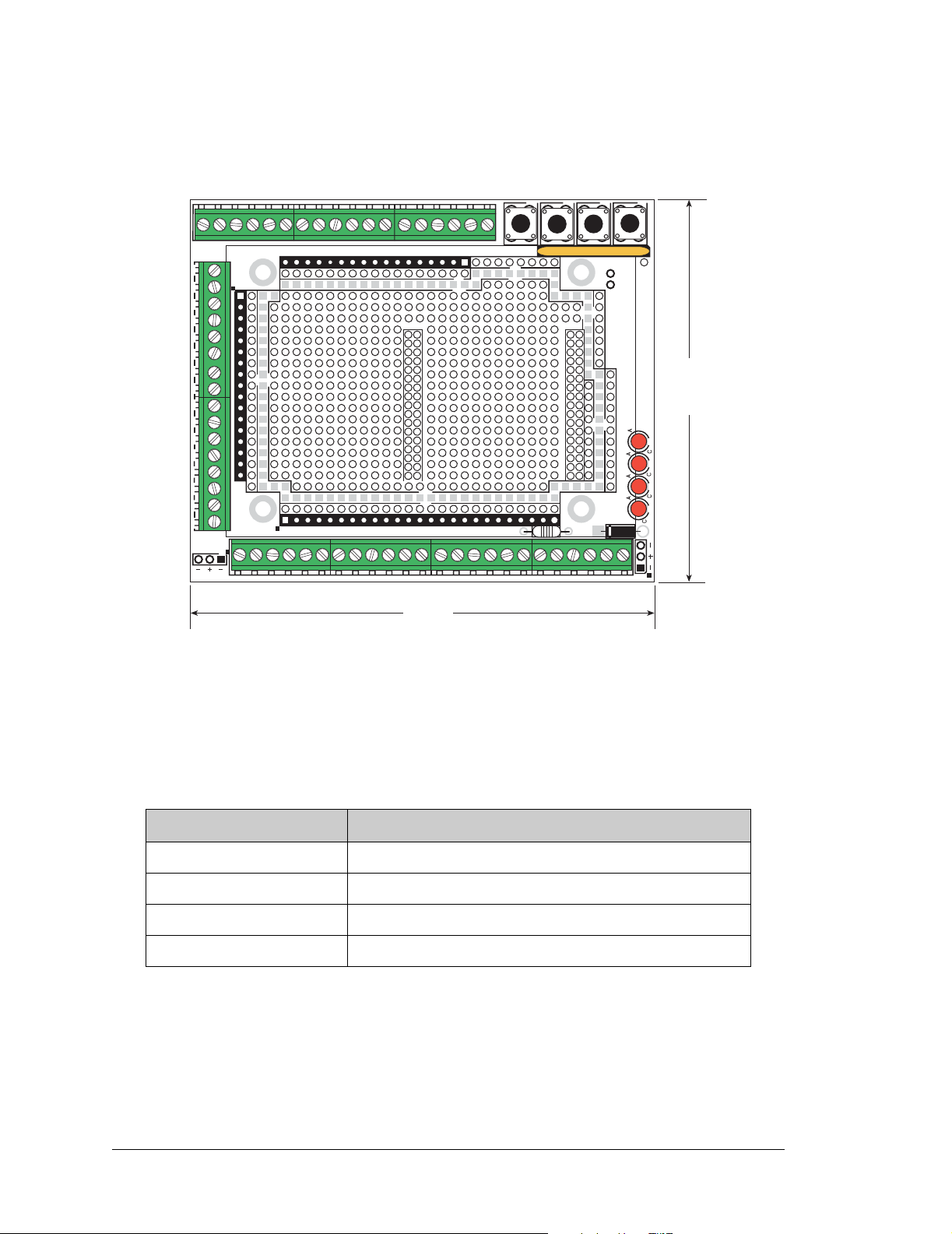
B.1 Mechanical Dimensions and Layout
Figure B-1 shows the mechanical dimensions and layout for the LP3500 Prototyping Board.
GND VIN GND VBAT EXT GND PWM2 PWM1 PWM0 GND AIN7 AIN6 AIN5 AIN4 AIN3 AIN2 AIN1 AIN0 GND
S4
J23
IN15 IN14 IN13 IN12 IN11 IN10 IN09 IN08 IN07 IN06 IN05 IN04 IN03 IN02 IN01 IN00
J11
GND
VIN
J12
J1
J13
J41
J3
3 V VBAT
GND RxE TxE GND RxC TxC GND RxB TxB GND + 485 GND +K OUT9 OUT8 OUT7 OUT6 OUT5 OUT4 OUT3 OUT2 OUT1 OUT0
J22
J2
J4
J42
J21
VIN
VIN
GND
GND
VIN
GND
R1
J43
4.14
(105)
S1
S2
S3
RN1
GND
VIN
(87)
3.41
GND
VIN
DS4 DS3 DS2 DS1
D1
J44
PWR
J5
Figure B-1. LP3500 Prototyping Board Dimensions
Table B-1 lists the electrical, mechanical, and environmental specifications for the Prototyping Board.
Table B-1. RCM3000/LP3500 Prototypi ng Board Specifications
Parameter Specification
Board Size 3.41" × 4.14" × 0.45" (87 mm × 105 mm × 11 mm)
Operating Temperature –40°C to +70°C
Humidity 5% to 95%, noncondensing
Prototyping Area 2.2" × 3.4" (56 mm × 86 mm) throughhole, 0.1" spacing
82 Fox (LP3500)
Page 89
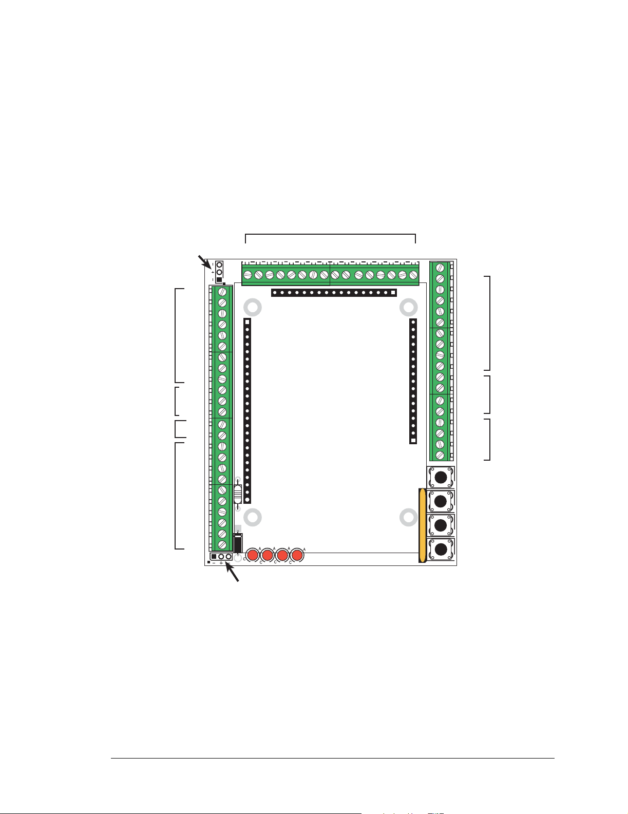
B.2 Using the Prototyping Board
B.2.1 Interface to LP3500
The Prototyping Board serves as a convenient interface for the LP3500, extending the IDC
headers to convenient screw-terminal connectors, and provides interfaces to the AC
adapter included with the Tool Kit and to a user-supplied external battery.
Figure B-2 shows the pinouts for the Prototyping Board.
Digital
IN04
IN05
Inputs
IN06
IN07
J1
IN08
IN09
IN10
IN11
IN12
IN13
IN14
IN15
IN15 IN14 IN13 IN12 IN11 IN10 IN09 IN08 IN07 IN06 IN05 IN04 IN03 IN02 IN01 IN00
J11
J22
J2
J21 J23
GND
AIN0
AIN1
AIN2
AIN3
AIN4
AIN5
AIN6
AIN7
GND
PWM0
PWM1
PWM2
GND
VBAT EXT
GND
VIN
GND
GND VIN GND VBAT EXT GND PWM2 PWM1 PWM0 GND AIN7 AIN6 AIN5 AIN4 AIN3 AIN2 AIN1 AIN0 GND
S4
Pushbutton
S3
Analog
Inputs
PWM
Outputs
Power
Supply
Switches
S2
S1
RS-232
RS-485
Digital
Outputs
External
Battery
Connection
GND
RxE
TxE
GND
RxC/CTS
TxC/RTS
GND
RxB
TxB
GND
RS-485+
RS-485
GND
K
+K
OUT9
OUT8
OUT7
OUT6
OUT5
OUT4
OUT3
OUT2
OUT1
OUT0
3 V VBAT
J6
J3
J5
J12
J41 J42
J43
R1
J44
D1
PWR
Raw DC
Power
Input
IN00
IN01
IN02
IN03
J4
DS4 DS3 DS2 DS1
LEDs
Figure B-2. LP3500 Prototyping Board Pinout
NOTE: The LP3500 must be plugged in to the Prototyping Board
as described in
Chapter 2, “Getting Started,” for these signals to be available.
User’s Manual 83
Page 90

B.2.2 Demonstration Board
The Prototyping Board is actually both a demonstration board and a prototyping board.
As a demonstration board, it can be used to demonstrate the functionality of the
LP3500
right out of the box without any modifications to either board. There are no jumpers or dip
switches to configure or misconfigure on the Prototyping Board so that the initial setup is
very straightforward.
The Prototyping Board comes with the basic components necessary to demonstrate the
operation of the LP3500. Four LEDs (DS1–DS4) are connected to PD0–PD3, and four
switches (S1–S4) are connected to PE0, PE1, PE4, and PE5 to demonstrate the i nterface to
the Rabbit 3000 microprocessor.
NOTE: Before running sample programs based on the LP3500, you will have to plug in
the LP3500 to the Prototyping Board
as described in Chapter 2, “Getting Started.”
B.2.3 Prototyping Area
Small to medium cir cuit s can b e pro toty ped u sin g po int -
to-point wiring with 20 to 30 A WG
wire on the prototyping area. Raw DC input, VIN, and GND lines surround the prototyping area.
The resistor pack located next to the pushbutton switches may be removed to disconnect
the LEDs and pushbutton switches from the Prototyping Board circuits, giving your
LP3500 exclusive access to what you may develop in the prototyping area.
+K and VIN are tied together by resistor R1 located beside header J44. Cut off R1 if you
intend to supply a separate +K.
84 Fox (LP3500)
Page 91
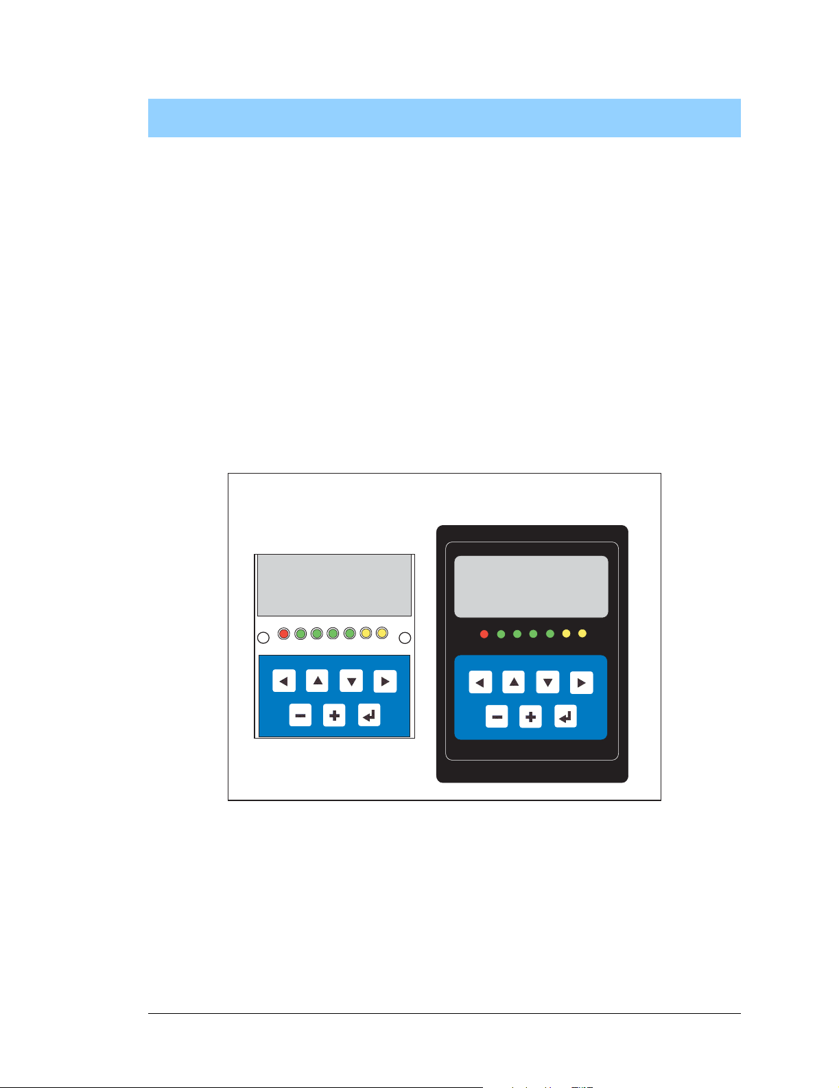
APPENDIX C. LCD/KEYPAD MODULE
An optional LCD/keypad is available for the LP3500. Appendix C
describes the LCD/keypad and provides the software APIs to
make full use of the LCD/keypad.
C.1 Specifications
Two optional LCD/keypad modules—with or without a panel-mounted NEMA 4 waterresistant bezel—are available for use with the LP3500. They are shown in Figure C-1.
LCD/Keypad Modules
Figure C-1. LCD/Keypad Modules Models
LCD/keypad modules sold prior to the launch of the LP3500 might not be voltagecompatible with the LP3500. Contact your Z-World sales representative or your authorized
Z-World distributor for further assistance in purchasing an LCD/keypad module.
Mounting hardware and a 127 mm (5") or 60 cm (24") extension cable are also available
for the LCD/keypad module through your Z-World sales representative or authorized
distributor.
User’s Manual 85
Page 92
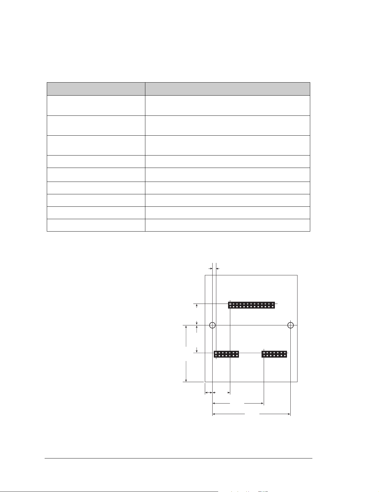
Table C-1 lists the electrical, mechanical, and environmental specifications for the
LCD/keypad module.
Table C-1. LCD/Keypad Specifications
Parameter Specification
Board Size
Bezel Size
Temperature
2.60" × 3.00" × 0.75"
(66 mm × 76 mm × 19 mm)
4.50" × 3.60" × 0.30"
(114 mm × 91 mm × 7.6 mm)
Operating Range: 0°C to +50°C
Storage Range: –40°C to +85°C
Humidity 5% to 95%, noncondensing
Power Consumption
1.5 W maximum with backlight on
*
Connections Connects to header J9 (Display Interface) on LP3500
LCD Panel Size 122 × 32 graphic display
Keypad 7-key keypad
LEDs Seven user-programmable LEDs
* The backlight adds approximately 650 mW to the power consumption.
The LCD/keypad module has 0.1"
IDC header sockets at J1, J2, and J3
0.100
(2.5)
for physical connection to other
boards or ribbon cables. Figure C-2
shows the LCD/keypad module footprint. These values are relative to one
(15.4)
of the mounting holes.
0.607
J1
(19.5)
(40.6)
1.600
0.200
(5.1)
0.768
0.500
(12.7)
J2
1.450
(36.8)
2.200
(55.9)
J3
Figure C-2. User Board Footprint for
LCD/Keypad Module
86 Fox (LP3500)
Page 93
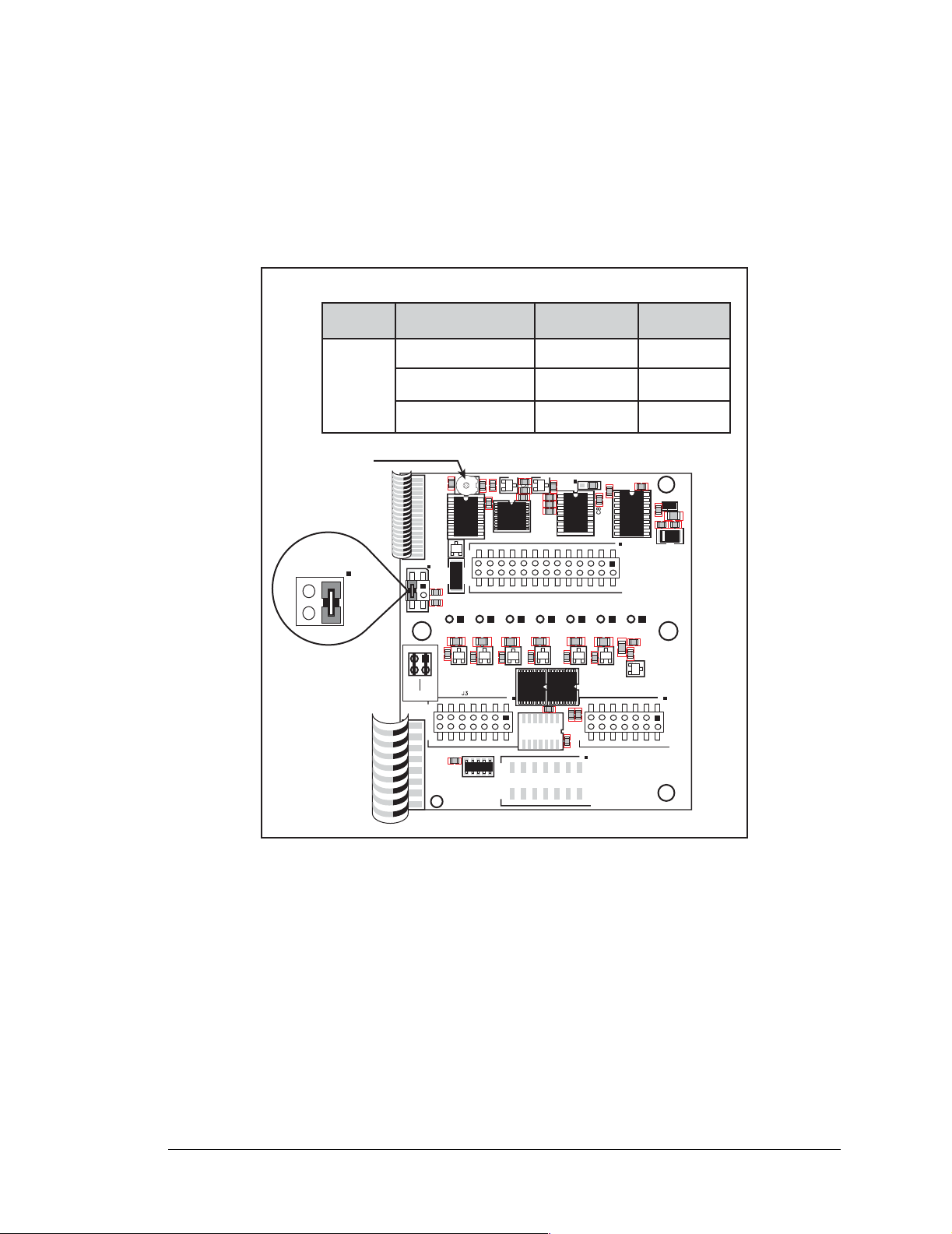
C.2 Contrast Adjustment
Depending on when you acquired your LCD/keypad module, you will be able to set the
contrast on the LCD display by adjusting the potentiometer at R2 or by setting the voltage
for 2.8 V by setting the jumper across pins 1–2 on header J5 as shown in Figure C-3. Only
one of these two options is available on a given LCD/keypad module
LCD/Keypad Module Jumper Configurations
Header
Description
2.8 V
Pins
Connected
12
Factory
Default
×
J5
Contrast
Adjustment
J5
3
4
1
2
J5
3
4
OTHER
3.3 V
n.c. = 5 V
KP1
3.3 V
5 V
R2
C2
U3
LCD1
Q1
R25
R8
R26
R11
J5
LP3500
2.8 V
R13
1
Q4
2
R17
C17
C1
D2
C6
C3
R1
C9
C7
U4
R14
R20
Q6
Q7
R23
R22
U6
U7
RN1
J4
34
n.c.
D1
JP1
C5
U2
R4
R5
C11
R10
R9
R19
Q3
Q2
U5
C14
R24
C15
C16
C4
R3
U1
C10
CR1
R6
C13
C12
R7
J1
R12
R15
R18
R16
Q5
R21
Q8
J2
DISPLAY
BOARD
Part No. 101-0541
Figure C-3. LCD/Keypad Module Contrast Adjustment
NOTE: Older LCD/keypad modules that do not have a header at J5 or a contrast adjust-
ment potentiometer at R2 are limited to operate only at 5 V, and will not work with the
LP3500. The older LCD/keypad modules are no longer being sold.
User’s Manual 87
Page 94
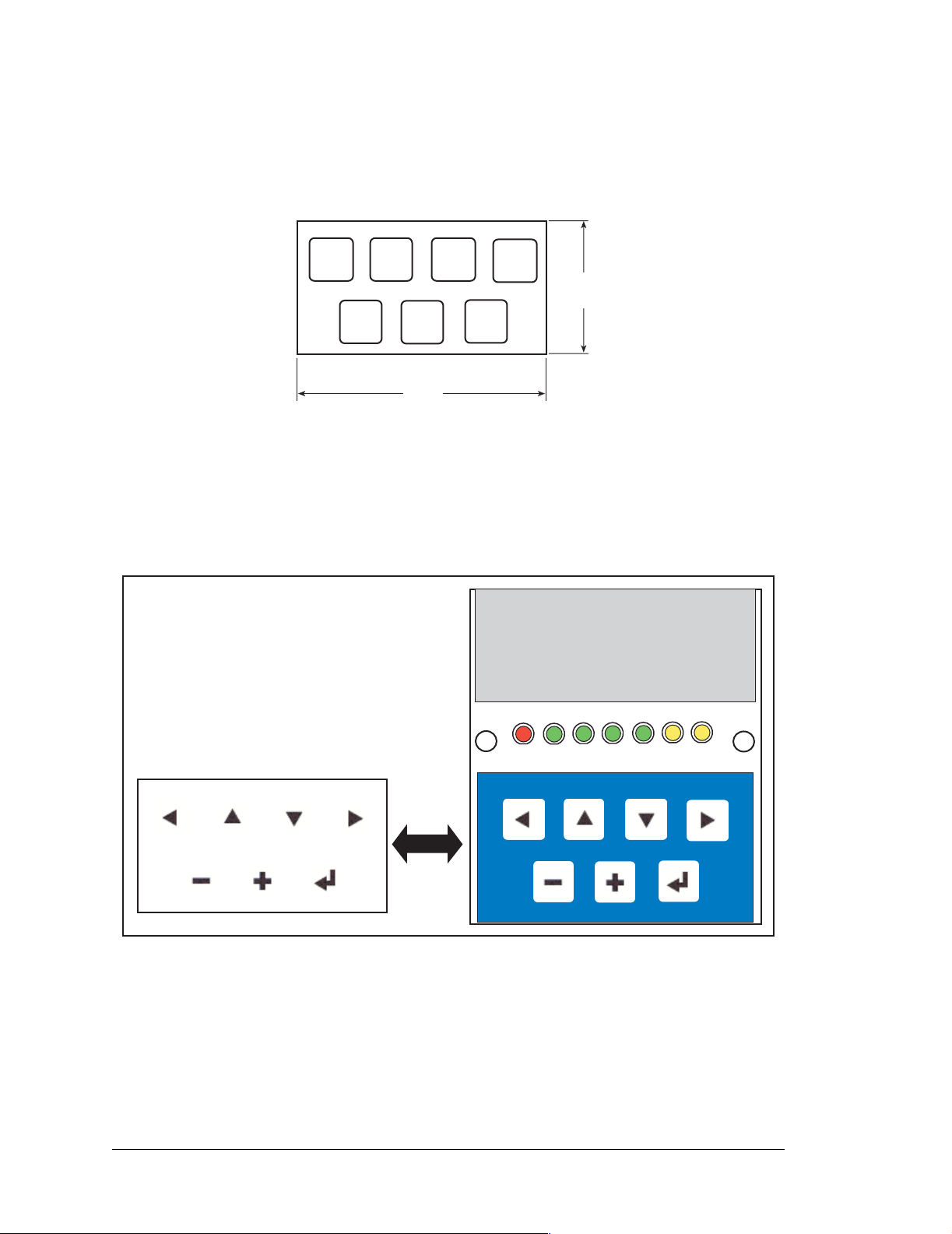
C.3 Keypad Labeling
The keypad may be labeled according to your needs. A template is provided in Figure C-4
to allow you to design your own keypad label insert.
1.10
(28)
2.35
(60)
Figure C-4. Keypad Template
To replace the keypad legend, remove the old legend and insert your new legend prepared
according to the template in Figure C-4. The keypad legend is located under the blue keypad matte, and is accessible from the left only as shown in Figure C-5.
Keypad label is located
under the blue keypad matte.
Figure C-5. Removing and Inserting Keypad Label
88 Fox (LP3500)
Page 95
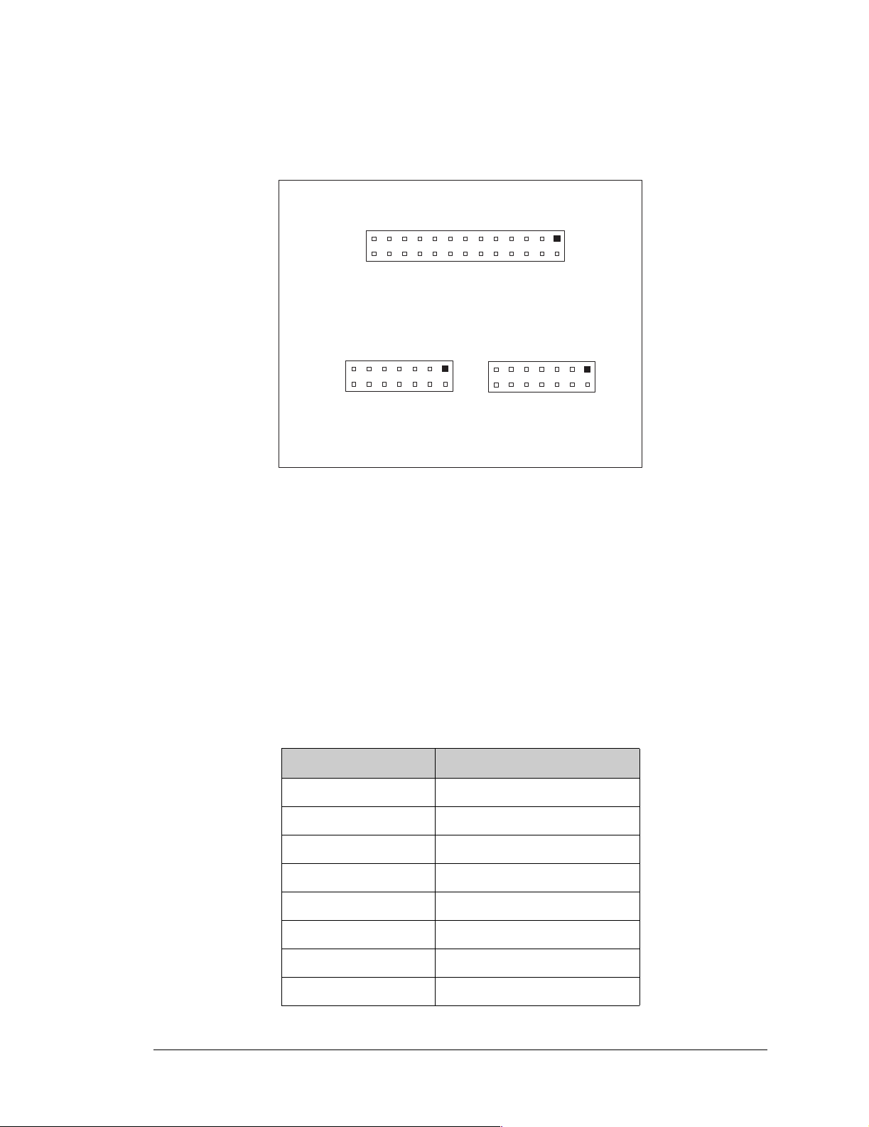
C.4 Header Pinouts
Figure C-6 shows the pinouts for the LCD/keypad module.
DB6B
DB4B
DB2B
DB0B
A1B
A3B
GND
LED7
LED5
LED3
LED1
J1
/RES
VCC
LED4
LED7
GND
LED2
LED5
LED6
/CS
+5BKLT
LED3
LED4
LED2
LED1
/RES
/CS
VCC
+5BKLT
J2
GND
GND
DB7B
DB6B
DB4B
DB7B
DB5B
DB5B
DB3B
DB2B
DB3B
DB1B
DB0B
A1B
A0B
DB1B
A0B
A2B
A3B
A2B
GND
J3
GND
LED6
GND
GND
Figure C-6. LCD/Keypad Module Pinouts
NOTE: Note that there are no connections from headers J2 and J3 of the LCD/keypad
module to the LP3500. These headers interface to the keypad and to the LEDs on the
LCD/keypad module, and need to be interfaced to the digital I/O on the LP3500 if you
need keypad or LED functionality. The LEDs may be driven by an active signal either
in software or in hardware.
C.4.1 I/O Address Assignments
The LCD and keypad on the LCD/keypad module are addressed by the /CS strobe as
explained in Table C-2.
Table C-2. LCD/Keypad Module Address Assignment
Address Function
0xE000 Device select base address (/CS)
0xExx0–0xExx7 LCD control
0xExx8 LED enable
0xExx9 Not used
0xExxA 7-key keypad
0xExxB (bits 0–6) 7-LED driver
0xExxB (bit 7) LCD backlight on/off
0xExxC–ExxF Not used
User’s Manual 89
Page 96
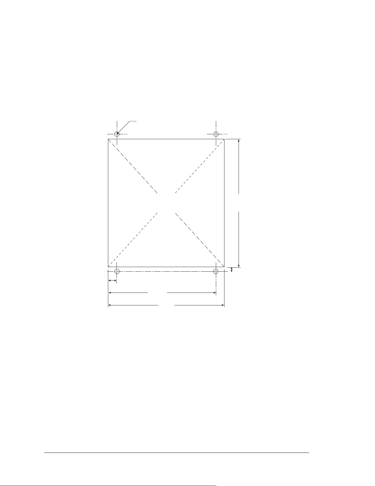
C.5 Bezel-Mount Installation
This section describes and illustrates how to bezel-mount the LCD/keypad module.
Follow these steps for bezel-mount installation.
1. Cut mounting holes in the mounting panel in accordance with the recommended dimensions in Figure C-7, then use the bezel faceplate to mount the LCD/keypad module onto
the panel.
0.125 D, 4x
(3)
CUTOUT
0.230
(5.8)
2.870
(72.9)
3.100
(78.8)
Figure C-7. Recommended Cutout Dimensions
3.400
(3.3)
0.130
(86.4)
2. Carefully “drop in” the LCD/keypad module with the bezel and gasket attached.
90 Fox (LP3500)
Page 97
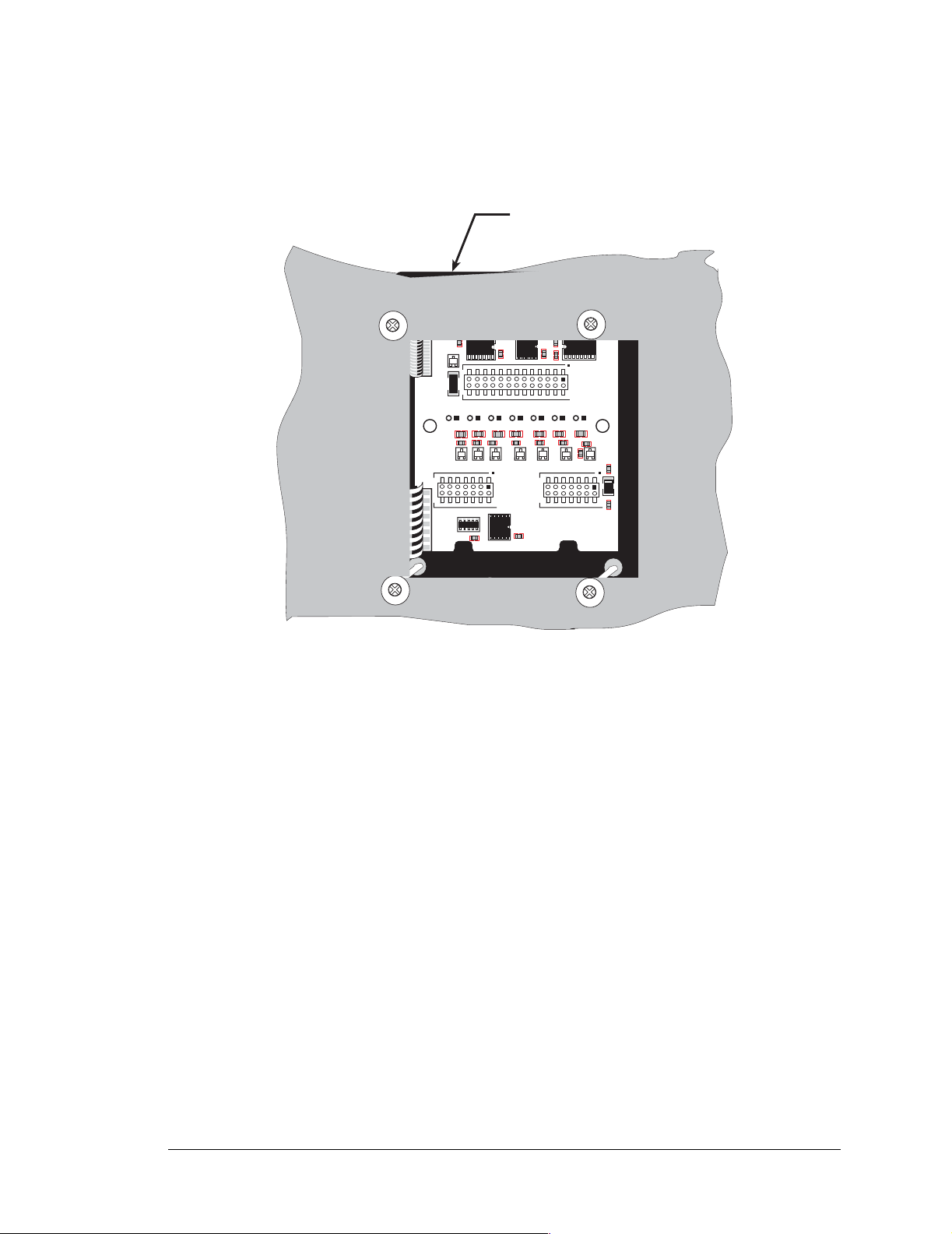
3. Fasten the unit with the four 4-40 screws and washers included with the LCD/keypad
module. If your panel is thick, use a 4-40 screw that is approximately 3/16" (5 mm)
longer than the thickness of the panel.
Bezel/Gasket
Panel
DISPLAY BOARD
U1
C1
R2
R9
R10
Q2 Q3
C2
R5
R4
R3
R11
R12
Q5 Q6
Q4
RN1
U4
C8
Q1
D1
R1
KP1
J2
U3
U2
C4
C3
R17
J1
R7
R8
R6
R14
R13
R15
R18
C5
Q8
Q7
C7
R16
J3
C6
Figure C-8. LCD/Keypad Module Mounted in Panel (rear view)
Carefully tighten the screws until the gasket is compressed and the plastic bezel faceplate is touching the panel.
Do not tighten each screw fully before moving on to the next screw . Apply only one or
two turns to each screw in sequence until all are tightened manually as far as they can
be so that the gasket is compressed and the plastic bezel faceplate is touching the panel.
User’s Manual 91
Page 98
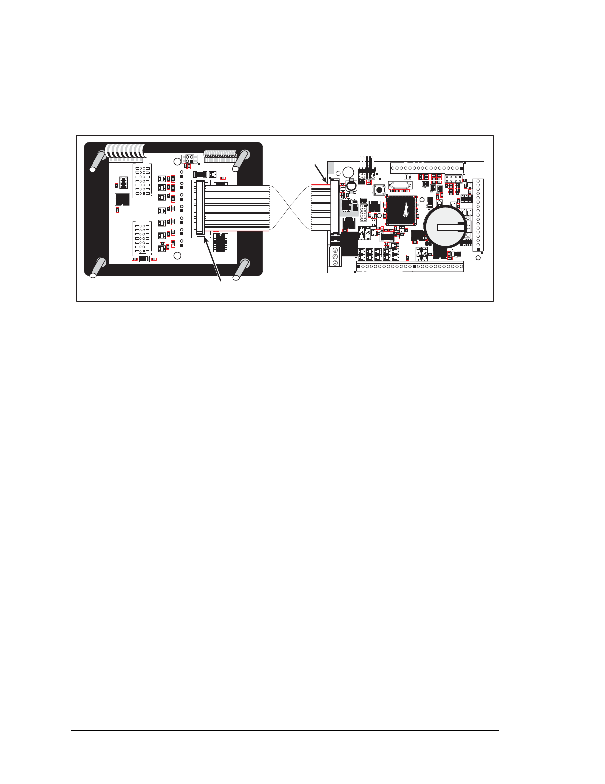
C.6 Connect the LCD/Keypad Module to Your LP3500
The LCD/keypad module can be located as far as 2 ft. (60 cm) away from the LP3500, and
is connected via a ribbon cable as shown in Figure C-9.
KP1
J2
RN1
C8
U4
C7
J3
C6
R9
Q2 Q3
R10
R11
Q4
R12
Q5 Q6
R13
R14
Q7
R18
R15
Q8
C5
R16
D1
J5
R25
R26
R2
R3
R4
R5
R6
R7
R8
Q1
R1
C1
U1
C2
DISPLAY BOARD
U2
C3
R17
C4
U3
J1
Pin 1
EXT
GND
DISPLAY
R55
R56
NO
COM
NC
RELAY
PORT
PROGRAM
RP14
R54
Q20
C65
R58
R51
RP13
C70
U13
C64
J9
C66
J6
U11
D33Q14
U12
C67
D32
Q13
K1
Q16
Q17
D34
J8
GND
OUT2
OUT0
OUT1
GND VIN GND
VBAT
PWM0
PWM2
J2
J5
R49
R50
RESET
S1
U9
U10
C60
R48
C59
R45
R47
R44
Q12
C61
Y2
R33
R43
Q10
D28
D30
OUT6
OUT4
OUT3
OUT5
PWM1
D22
C40
R32
Y1
C50
R36
R40 C54
C44
BT1
C43
U8
U3
C55
R39
R41
R34
C51
C53
Q6
C48
R38
D18
D21
R42
Q5
Q8
D25
R37
D26
D20
+K GND 485 + GND TxB RxB GND TxC RxC GND TxE RxE GND
OUT7
OUT8
OUT9
C37
R29
R31
R57
C36
D19
R22
R26
R25
R20
C33
C26
R30
R23
C29
C22
Battery
RP17
D15 D17
U1
AIN0 AIN1 AIN2 AIN3 AIN4 AIN5 AIN6 AIN7 GND GND
AIN0 AIN1 AIN2 AIN3
R1
J3
D1
R9
R7
R17
R18
R16
R6
C3
R13
RN1
C2
C10 C13
C24
D8
C8
Q22
D2
D4
C6
D7
D13
D11
D5
C20
C12
C15
RN2
C19
C16
IN00 IN01 IN02 IN03 IN04 IN05 IN06 IN07 GND IN08 IN09 IN10 IN11 IN12 IN13 IN14 IN15
J1
J4
Pin 1
Figure C-9. Connecting LCD/Keypad Module to LP3500
Note the locations and connections relative to pin 1 on both the LP3500 and the LCD/keypad module.
Z-World offers two different lengths of ribbon cable–5" (127 mm) and 2 ft. (60 cm).
Contact your authorized Z-World distributor or a Z-World sales representative at
+1(530)757-3737 for more information.
92 Fox (LP3500)
Page 99

C.7 LCD/Keypad Module Function APIs
The LCD/keypad module is normally off. Add the devPowerSet function call after
brdInit to turn on the LCD/keypad buffers.
brdInit(); // Initialize the LP3500
devPowerSet(DISPDEV, 1); // Enable LCD/keypad buffer
C.7.1 LEDs
When power is applied to the LCD/keypad module for the first time, the red LED (DS1)
will come on, indicating that power is being applied to the LCD/keypad module. The red
LED is turned off when the brdInit function executes.
One function is available to control the LEDs, and can be found in the LCD122KEY7.LIB
library in the Displays directory.
void dispLedOut(int led, int value);
LED on/off control. This function will only work when the LCD/keypad module is connected to the
LP3500.
PARAMETERS
led is the LED to control.
0 = LED DS1
1 = LED DS2
2 = LED DS3
3 = LED DS4
4 = LED DS5
5 = LED DS6
6 = LED DS7
value is the value used to control whether the LED is on or off (0 or 1).
0 = off
1 = on
RETURN VALUE
None.
SEE ALSO
brdInit
User’s Manual 93
Page 100

C.7.2 LCD Displ a y
The functions used to control the LCD display are contained in the GRAPHIC.LIB library
located in the Dynamic C DISPLAYS\GRAPHIC library directory. When x and y coordi-
nates on the display screen are specified, x can range from 0 to 121, and y can range from
0 to 31. These numbers represent pixels from the top left corner of the display.
void glInit(void);
Initializes the display devices, clears the screen.
RETURN VALUE
None.
SEE ALSO
glDispOnOFF, glBacklight, glSetContrast, glPlotDot, glBlock, glPlotDot,
glPlotPolygon, glPlotCircle, glHScroll, glVScroll, glXFontInit, glPrintf,
glPutChar, glSetBrushType, glBuffLock, glBuffUnlock, glPlotLine
void glBackLight(int onOff);
Turns the display backlight on or off.
PARAMETER
onOff turns the backlight on or off
1—turn the backlight on
0—turn the backlight off
RETURN VALUE
None.
SEE ALSO
glInit, glDispOnoff, glSetContrast
void glDispOnOff(int onOff);
Sets the LCD screen on or off. Data will not be cleared from the screen.
PARAMETER
onOff turns the LCD screen on or off
1—turn the LCD screen on
0—turn the LCD screen off
RETURN VALUE
None.
SEE ALSO
glInit, glSetContrast, glBackLight
94 Fox (LP3500)
 Loading...