

CP96TEL2400
P R E L I M I N A R Y
1
1
P
RELIMINARY
C
USTOMER
P
ROCUREMENT
S
PECIFICATION
Z90219/213/212/211/218
1
Z8
®
D
IGITAL
T
ELEVISION
C
ONTROLLERS
FEATURES
Z8-Based CMOS Microcontroller for Consumer
Television, Cable Box, and Satellite Receiver
Applications.
■
42-Pin SDIP Package
■
Z8
®
Microcontroller Core at 6 MHz
■
Mask ROM sizes Available in 8, 12 and 16 Kbytes
■
Eleven Pulse Width Modulators
■
On-Chip Infrared (IR) Capture Registers
■
Four Channel 3-bit Analog-to-Digital Converter
■
Twenty General Purpose I/O Pins
■
I
2
C Serial Communication Port)
On Screen Display (OSD) Section
■
Supports Displays up to 10 rows by 24 Columns with
256 Characters
■
Character Cell Resolution of 14 Pixels by 18 Scan lines
■
Variable Inter-row Spacing from 0-15 Horizontal Scan
Lines
■
Foreground and Background Colors Fully
Programmable by Character
GENERAL DESCRIPTION
The Z9021x Digital Television Controller (DTC) family is
Zilog’s latest and most powerful Z8-based DTC product offering. These parts feature larger system RAM and ROM
options, together with a host of new features including a
new color palette system, flexible inter-row spacing, higher
character cell resolution, background mesh effect, dedicated I.R. capture registers, on-chip Analog-to-Digital conversion, and a hardware Master mode I
2
C interface. The familiar Z8 core in combination with these advanced features
makes the Z9021x family an ideal choice for low to midrange televisions in both PAL and NTSC markets.
The Z9021x family consists of two basic device types;
Z9020x and Z9021x. The only difference between the two
types is the presence of a hardware I
2
C serial communication port and half-tone OSD circuitry on the Z9021x family.
Of course I
2
C communication is supported on the Z9020x
family in software with the dedication of any two I/O pins to
the task.
The Z9021x family takes full advantage of the Z8’s expanded register file space to offer greater flexibility in On
Screen Display creation.
Device
ROM
(KB)
RAM*
(Bytes)
I/O
Lines
Voltage
Range
Z90211 16 (OTP) 237 20 4.5V to 5.5V
Z90218 8 237 20 4.5V to 5.5V
Z90212 12 237 20 4.5V to 5.5V
Z90213 16 237 20 4.5V to 5.5V
Z90219 32 (ext.) 237 N/A 4.5V to 5.5V
Note: OTP and Z9021x products under development

Z90219/213/212/211
Z8
®
Digital Television Controllers Zilog
2
P R E L I M I N A R Y
CP96TEL2400
BLOCK DIAGRAM
Figure 1. Functional Block Diagram
8/12/16K Byte
Program ROM
Z8 CPU
Core
RESET
Oscillator
WDT
Counter
Timer
Counter
Timer
3-bit
ADC
IR
Counter
Port3
256 Byte
Register File
Port2
Port4
On Screen
Display
240 by 11-bit
Character RAM
9K by 7-bit
Character ROM
PWM 11
PWM 1
to
PWM 10
(14-bit)
(6-bit)
XTAL1
XTAL2
/RESET
ADC0
ADC1
ADC2
ADC3
IRIN
P30
P31
P34
P35
P21
P22
P23
P24
P25
P26
P27
P40
P41
P42
P43
P44
P45
P46
P47
P20
OSDX1
OSDX2
HSync
VSync
R
G
B
VBlank
PWM11
PWM1
PWM2
PWM3
PWM4
PWM5
PWM6
PWM7
PWM8
PWM9
PWM10
& 10 by 8-bit
SCLK0
SDATA0
I
2
C
P1
P2
P3
P4
P5
P6
P7
Output
Port
Interface
SCLK1
SDATA1
HLFTN
Z9021x ONLY
Z9021x ONLY
Z90219/213/212/211
Zilog Z8
®
Digital Television Controllers
CP96TEL2400
P R E L I M I N A R Y
3
1
PIN IDENTIFICATION
PWM11/P7
PWM6/P6
PWM5/P5
PWM4/P4
PWM3/P3
PWM2/P2
PWM1/P1
P40
P34/ADC3
P35/ADC2
P41/ADC1
P31/ADC0
AGND
P42
P43
P30
P44/PWM7
P45/PWM8
P46/PWM9
P47/PWM10
P20/HLFTN
P27/SDATA1
P26/SCLK1
P25/SDATA0
P24/SCLK0
P23
P22
IRIN
P21
VCC
/RESET
XTAL2
XTAL1
GND
OSDX2
OSDX1
VSYNC
HSYNC
VBLANK
R
G
B
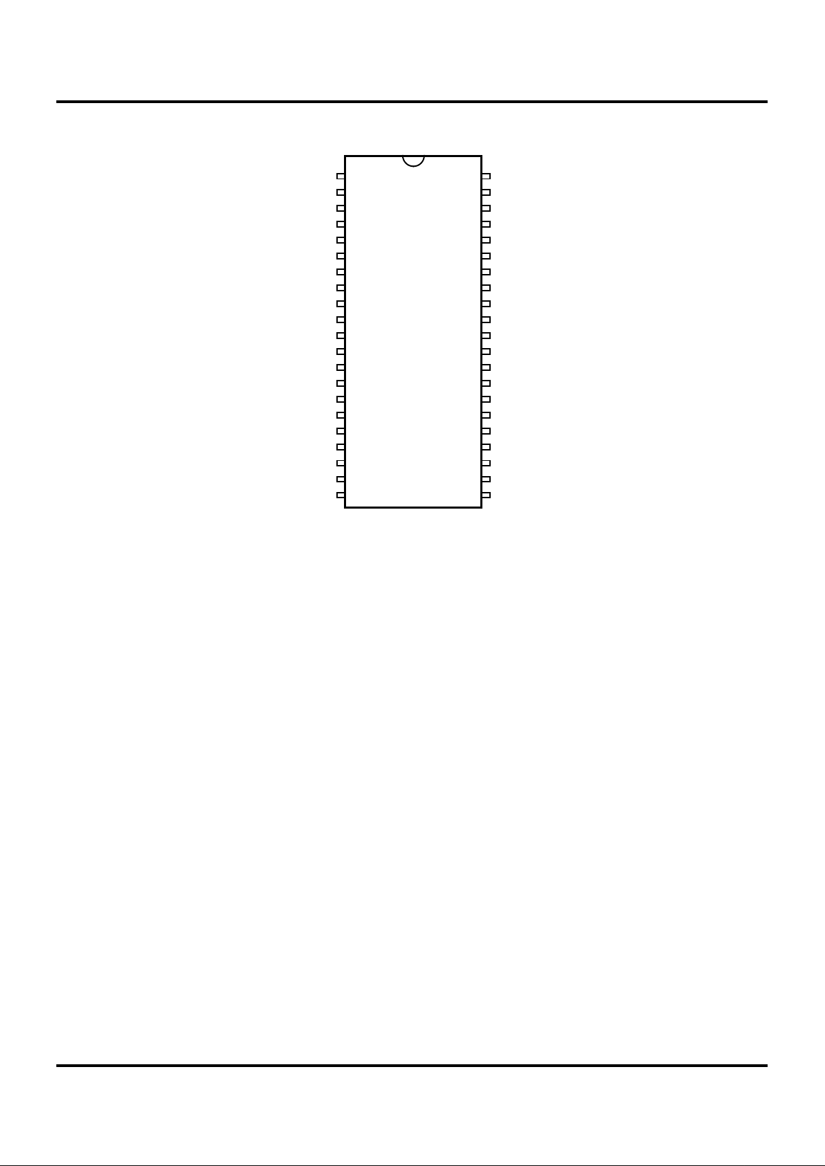
42
Z9021x
(T op View)
1
21 22

Z90219/213/212/211
Z8
®
Digital Television Controllers Zilog
4
P R E L I M I N A R Y
CP96TEL2400
PIN IDENTIFICATION
Table 1. Z9021x 42L SDIP Package
Pin Function Pin Number I/O/PWR Reset State Name
+5 V olts 34 PWR PWR VCC
0 V olts 30,13 PWR PWR GND,A GND
Infra Red remote capture input 36 I I IRIN
14-bit Pulse Width Modulator
output
1 O O PWM11
6-bit Pulse Width Modulator
output
20,19,18,17,2,3,4,
5,6,7
O O PWM[10:1]
Fixed output ports 7,6,5,4,3,2,1 O O P[1:7]
Bit programmable
Input/Output ports
42,41,40,39,38,37,
35,21
I/O I P2[7:0]
Half tone output 21 O I HLFTN
I
2
C Data 40,42 I/O I SDATA0,1
I
2
C Clock 39,41 O I SCLK0,1
Fixed output ports 10,9 O O P3[5:4]
Fixed input ports 12,16 I I P3[1:0]
Bit programmable
Input/Output ports
20,19,18,17,15,14,
11,8
I/O I P4[7:0]
Crystal oscillator input 31 I I XTAL1
Crystal oscillator output 32 O O XTAL2
Dot clock oscillator input 28 I I OSDX1
Dot clock oscillator output 29 O O OSDX2
Horizontal Sync 26 I I HSYNC
Vertical Sync 27 I I VSYNC
Video blank 25 O O VBLANK
Video R,G,B 24,23,22 O O R,G,B
3-bit Analog to Digital
converter input
9,10,11,12 AI I ADC[3:0]
Device reset 33 I I /RESET

Z90219/213/212/211
Zilog Z8
®
Digital Television Controllers
CP96TEL2400
P R E L I M I N A R Y
5
1
ABSOLUTE MAXIMUM RATINGS
Stresses greater than those listed under Absolute Maximum Ratings may cause permanent damage to the device. This is a stress rating only; operation of the device at
any condition above those indicated in the operational sec-
tions of these specifications is not implied. Exposure to absolute maximum rating conditions for extended periods
may affect device reliability
Table 2.
Symbol Parameters Min Max Units Notes
V
cc
Power Supply
Voltage
-0.3 +7 V
V
i
Input V oltage -0.3 V
cc
+0.3 V
V
o
Output V oltage -0.3 V
cc
+0.3 V
I
oh
Output Current
High
-10 mA per pin
I
oh
Output Current
High
-100 mA per device
I
ol
Output Current
Low
20 mA per pin
I
ol
Output Current
Low
200 mA per device
T
a
Operating
Temperature
070
o
C
T
STG
Operating
Temperature
-55 150
o
C

Z90219/213/212/211
Z8
®
Digital Television Controllers Zilog
6
P R E L I M I N A R Y
CP96TEL2400
DC CHARACTERISTICS
T
A
=0
o
C to + 70
o
C; V
CC
= +4.5V to +5.5V; F
OSC
= 6MHz
Table 3.
Symbol Parameter Min Typical Max Units Conditions
V
cc
Power Supply
Voltage
4.75 5.00 5.25 V
V
ih
Input V oltage High 0.7V
cc
3.0 V
cc
V
V
il
Input V oltage Low 0 1.48 0.2V
cc
V
V
ihc
Input XTAL/Osc in
High
0.8V
cc
3.2 V
cc
V
V
ilc
Input XTAL/Osc In
Low
0.98 0.07V
cc
V
V
oh
Output V oltage
High
V
cc
-0.4 4.75 V I
oh
=-0.75mA
V
ol
Output V oltage
Low
0.16 0.4 V I
ol
=1.00mA
V
hy
Schmitt Hysteresis 0.1V
cc
0.8 V
I
ir
Reset Input
Current
-46 -80 uA V
rl
=0V
I
il
Input Leakage -3.0 0.01 3.0 uA 0V,V
cc
I
ol
Tri-State Leakage -3.0 0.02 3.0 uA 0V,V
cc
I
cc
Supply Current 13.2 20 mA All inputs at rail;outputs floating
I
cc1
Sleep Mode
Current
3.2 6 mA All inputs at rail;outputs floating
I
cc2
Stop Mode Current 0.1 10 uA All inputs at rail;outputs floating
Note: Typical values measured at 25
o
C. Minimum and Maximum values given from 0oC to 70oC.

Z90219/213/212/211
Zilog Z8® Digital Television Controllers
CP96TEL2400 P R E L I M I N A R Y 7
1
AC CHARACTERISTICS
Table 4.
No Symbol Parameter Min Max Unit
1T
p
C Input clock period 166 1000 ns
2T
r
C, TfC Clock input raise and fall 25 ns
3T
w
C Input clock width 35 ns
4T
w
T
in
L Timer input low width 70 ns
5T
w
T
in
H Timer input high width 3TpC
6T
p
TinTimer input period 8TpC
7T
r
T
in
, TrTinTimer input raise and fall 100 ns
8T
w
IL Int request input low 70 ns
9T
w
IH Int request input high 3TpC
10 T
d
POR Power-On reset delay 25 100 ms
11 T
d
LVIRES Low voltage detect to
internal RESET condition
200 ns
12 TwRES Reset minimum width 5TpC
13 T
dHs
Ol H
sync
start to V
osc
stop 2TpV3T
p
V
14 T
dHs
Oh H
sync
start to V
osc
start 1TpV

Z90219/213/212/211
Z8® Digital Television Controllers Zilog
8 P R E L I M I N A R Y CP96TEL2400
AC TIMING DIAGRAMS
Figure 2. Timing Diagram
1
2
2
3
3
4
5
6
7
8
9
10
11
12
13
14
XTAL1 TIN
IRQN
V
cc
Internal/RESET
External/RESET
HSYNC
OSCX2

Z90219/213/212/211
Zilog Z8® Digital Television Controllers
CP96TEL2400 P R E L I M I N A R Y 9
1
© 1997 by Zilog, Inc. All rights reserved. No part of this
document may be copied or reproduced in any form or by
any means without the prior written consent of Zilog, Inc.
The information in this document is subject to change
without notice. Devices sold by Zilog, Inc. are covered by
warranty and patent indemnification provisions appearing
in Zilog, Inc. Terms and Conditions of Sale only. Zilog, Inc.
makes no warranty, express, statutory, implied or by
description, regarding the information set forth herein or
regarding the freedom of the described devices from
intellectual property infringement. Zilog, Inc. makes no
warranty of merchantability or fitness for any purpose.
Zilog, Inc. shall not be responsible for any errors that may
appear in this document. Zilog, Inc. makes no commitment
to update or keep current the information contained in this
document.
Zilog’s products are not authorized for use as critical
components in life support devices or systems unless a
specific written agreement pertaining to such intended use
is executed between the customer and Zilog prior to use.
Life support devices or systems are those which are
intended for surgical implantation into the body, or which
sustains life whose failure to perform, when properly used
in accordance with instructions for use provided in the
labeling, can be reasonably expected to result in
significant injury to the user.
Zilog, Inc. 210 East Hacienda Ave.
Campbell, CA 95008-6600
Telephone (408) 370-8000
FAX 408 370-8056
Internet: http://www.zilog.com

Z90219/213/212/211
Z8® Digital Television Controllers Zilog
10 P R E L I M I N A R Y CP96TEL2400
 Loading...