DS97TEL1902 1
1
P
RODUCT
S
PECIFICATION
Z90102/103/104
1
40-P
IN
L
OW
-C
OST
D
IGITAL
T
ELEVISION
C
ONTROLLER
FEATURES
8-Bit CMOS Microcontroller for Consumer
Television, Cable and Satellite Receiver Applications.
■
Lowest Cost DTC Family Member
■
Low Power Consumption
■
Fast Instruction Pointer - 1.5
m
s @ 4 MHz
■
Two Standby Modes - STOP and HALT
■
Low Voltage Detection/Voltage Sensitive Reset
■
Port 2 (8-Bit Programmable I/O) and Port 3 (2-Bit Input,
3-Bit Output) Register Mapped Ports
■
Port 6 (6-Bit Input and Tristate Comparator AFC Input)
Memory Mapped I/O Ports
■
All Digital CMOS Levels Schmitt-Triggered
■
Two Programmable 8-Bit Counter/Timers each with 6Bit Programmable Prescaler.
■
Six Vectored, Priority Interrupts from Six Different
Sources
■
Clock Speed up to 4 MHz
■
On-Chip Oscillator that Accepts a Crystal, Ceramic
Resonator, LC or External Clock Drive
■
Permanently Enabled
Watch-Dog/Power-On Reset Timer
■
3K x 6-Bit Character Generator ROM
■
120 x 7-Bit Video RAM
■
Mask Programmable 96-Character Set Display. The
90102 and 90103 6-Row x 20 Column Format, 12x15
Pixel Character Cell. The 90104 8-Row x 20 Column
Format 12x15 Pixel Character Cell. The 90102, 90103
90104 Capable of supporting English, Korean, Thai,
Chinese and Japanese High Resolution Characters.
■
Fully Programmable Color Attributes Including Row
Character, Row Background/Fringes, Frame
Background/Position, Bar Graph Color Change, and
Character Size.
■
Programmable Display Position and Character Size
Control
■
One Pulse Width Modulator (14-Bit Resolution) for
Voltage Synthesis Tuner Control.
■
Three Pulse Width Modulator (8-Bit Resolution) for
Picture Control
■
Three Pulse Width Modulators (6-Bit Resolution) for
Audio Control
GENERAL DESCRIPTION
The Z90102/3/4 40-pin Low-Cost Digital Television Controller are members of the Z8
®
STOP Mode MCU singlechip family with 4, 6, and 8 KB of ROM and 236 bytes of
RAM. The device is offered in a 40-pin package and is
CMOS compatible. The DTC offers mask programmed
ROM which enables the Z8
®
MCU to be used in a high volume production application device embedded with a custom program (customer supplied program) and combines
Device
ROM
(KB)
RAM*
(Bytes) I/O
Z90102 4 236 24
Z90103 6 236 24
Z90104 8 236 24
Note: *General-Purpose

Z90102/90103/90104
40-Pin Low-Cost Digital Television Controller Zilog
2 DS97TEL1902
GENERAL DESCRIPTION (Continued)
together with the Z86C27 and Z86127 to provide support
for mid range and low end TV applications.
Zilog’s DTC offers fast execution, efficient use of memory,
sophisticated interrupts, input/output bit manipulation capabilities, and easy hardware/software system expansion
along with low cost and low power consumption. The device provides an ideal performance and reliability solution
for consumer and industrial television applications.
The Z90102/3/4 architecture is characterized by utilizing
Zilog’s advanced Superintegration™ design methodology.
The device has an 8-bit internal data path controlled by a
Z8 microcontroller and On Screen Display (OSD) logic circuits and Pulse Width Modulators (PWM). On-chip peripherals include two register mapped I/O ports (Ports 2 and
3), interrupt control logic (one software, two external and
three internal interrupts) and a standby mode recovery input port (Port 3, P30).
The OSD control circuits support 6 rows x 20 columns of
characters. The character color is specified by row. One of
the six rows is assigned to show two kinds of colors for bar
type displays such as volume control. The OSD is capable
of displaying either low resolution (5 x 7 dot pattern) or high
resolution (11 x 15 dot pattern) characters.
A 14-bit PWM port provides enough voltage resolution for
a voltage synthesizer tuning system. Three 6-bit PWM
ports are used for controlling audio signal levels. Three 8bit PWM ports used to vary picture levels.
For DTC applications demanding powerful I/O capabilities, the Z90102/3/4 fulfills this with 24 I/O pins dedicated
to input and output. These lines are grouped into three
ports, and are configurable under software control to provide timing, status signals, parallel I/O and an address/data bus for interfacing to external memory.
There are three basic address spaces available to support
this wide range of configurations: Program Memory, Video
RAM, and Register File. The Register File is composed of
236 bytes of general-purpose registers, two I/O Port registers, 15 control and status registers and three reserved
registers.
To unburden the program from coping with the real-time
problems such as counting/timing and data communication, the DTC offers two on-chip counter/timers with a large
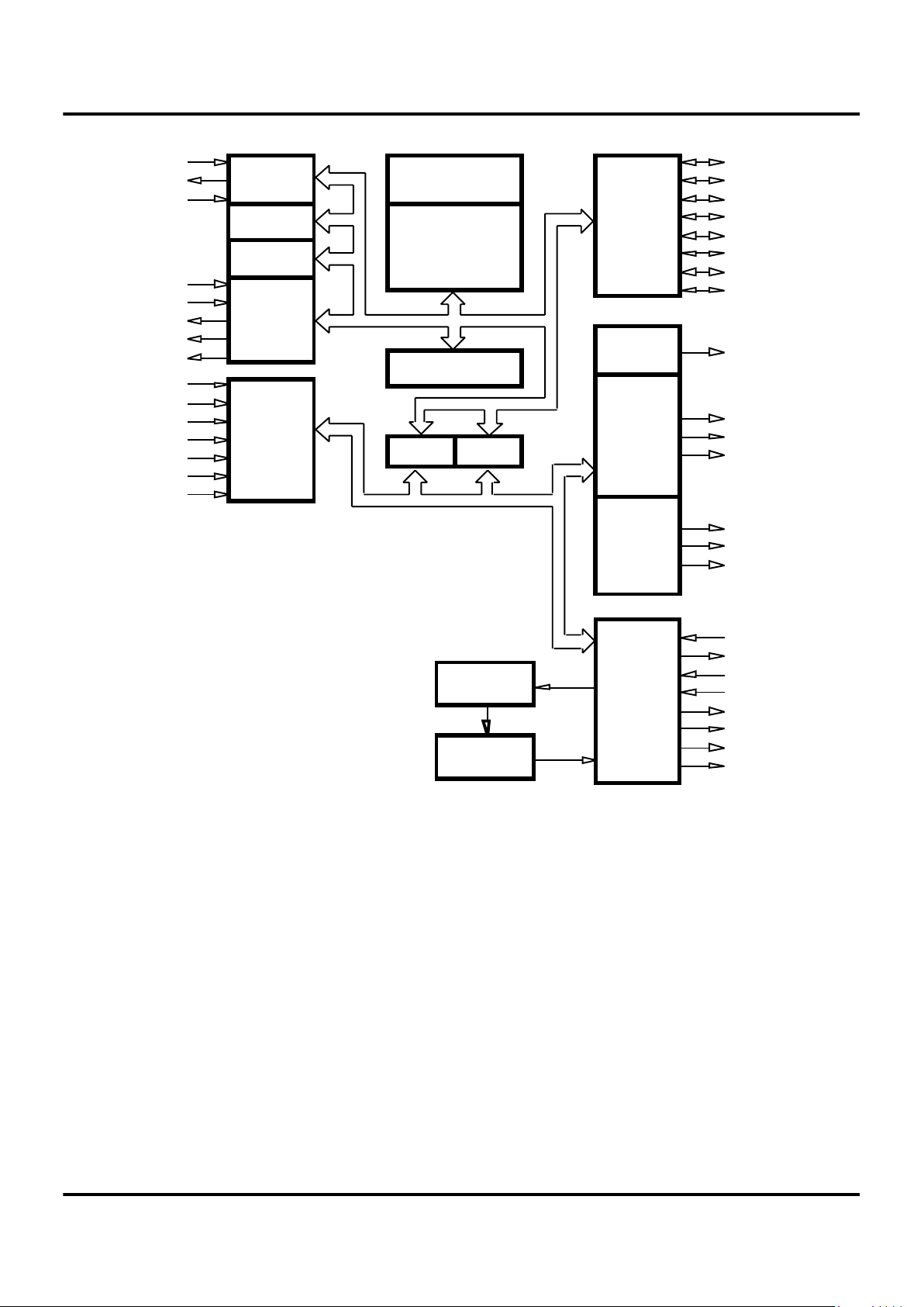
number of user selectable modes (Figure 1).
Notes: All signals with a preceding front slash, "/", are ac-
tive Low. For example, B//W (WORD is active Low); /B/W
(BYTE is active Low, only).
Power connections follow conventional descriptions below:
Connection Circuit Device
Power V
CC
V
DD
Ground GND V
SS

Z90102/90103/90104
Zilog 40-Pin Low-Cost Digital Television Controller
DS97TEL1902 3
1
Figure 1. Functional Block Diagram
Counter
Timer
Counter
Timer
4, 6 or 8 KB
Program ROM
RESET
Oscillator
WDT
Port 3/
Interrupt
Port 6
Z8 CPU
Core
Port 2
256 Byte
Register File
Port 1
A8-15 AD0-7
PWM 1
14 -bit
PWM 6
to
PWM 8
6-bit
On-Screen
Display
Port 0
120 Byte
Character RAM
3 Kbyte
Character ROM
P27
P26
P25
P24
P23
P22
P21
P20
PWM 6
PWM 7
PWM 8
OSCIN
OSCOUT
HSYNC
VSYNC
VRED
VGREEN
VBLUE
VBLANK
XTAL1
XTAL2
/RESET
P30
P31
P34
P35
P36
P60
P61
P62
P63
P64
P65
AFCIN
PWM 1
PWM 9
to
PWM 11
8-bit
PWM 9
PWM 10
PWM 11

Z90102/90103/90104
40-Pin Low-Cost Digital Television Controller Zilog
4 DS97TEL1902
PIN DESCRIPTION
Figure 2. 40-Pin Mask-ROM Plastic DIP
PWM1
P35
P36
P34
P31
P30
XTAL1
XTAL2
/RESET
P60
GND
P61
P62
VCC
P63
P64
P65
AFCIN
OSCIN
OSCOUT
PWM6
PWM7
PWM8
PWM9
PWM10
PWM11
P27
P26
P25
P24
P23
P22
P21
P20
VBLANK
VBLUE
VGREEN
VRED
VSYNC
HSYNC
21
Z90102
Z90103
Z90104
40-Pin DIP
1
20 40
Table 1. 40-Pin Mask-ROM Plastic DIP
40-Pin Name Function Direction
1 PWM1 Pulse Width Modulator 1 Output
2, 3 P35-36 Port 3, Pins 5, 6 Output
4 P34 Port 3, Pin 4 Output
5 P31 Port 3, Pin 1 Input
6 P30 Port 3, Pin 0 Input
7 XTAL1 Crystal Oscillator Input
8 XTAL2 Crystal Oscillator Output
9 /RESET System Reset Input
10 P60 Port 6, Pin 0 Input
11 GND Ground Input
12 P61 Port 6, Pin 1 Input
13 P62 Port 6, Pin 2 Input
14 V
CC
Power Supply Input
15, 16, 17 P63-65 Port 6, Pins 3, 4, 5 Input
18 AFC
IN
AFC V oltage Level Input
19 OSC
IN
Video Dot Clock Osc Input
20 OSC
OUT
Video Dot Clock Osc Output
21 HSYNC Horizontal Sync Input
22 VSYNC Vertical Sync Input
23 Vred Video Red Output

Z90102/90103/90104
Zilog 40-Pin Low-Cost Digital Television Controller
DS97TEL1902 5
1
24 Vgreen Video Green Output
25 Vblue Video Blue Output
26 Vblank Video Blank Output
27-34 P20-27 Port 2, Pins 0,1,2,3,4,5,6,7 In/Output
35 PWM11 Pulse Width Modulator 11 Output
36 PWM10 Pulse Width Modulator 10 Output
37 PWM9 Pulse Width Modulator 9 Output
38 PWM8 Pulse Width Modulator 8 Output
39 PWM7 Pulse Width Modulator 7 Output
40 PWM6 Pulse Width Modulator 6 Output
Table 1. 40-Pin Mask-ROM Plastic DIP
40-Pin Name Function Direction

Z90102/90103/90104
40-Pin Low-Cost Digital Television Controller Zilog
6 DS97TEL1902
PIN DESCRIPTION
XTAL1, XTAL2. (time-based input, output, respectively).
These pins connect to the internal parallel-resonant clock
crystal (4 MHz max) oscillator circuit with two capacitors
to GND. XTAL1 is also used as an external clock input.
SCLK System Clock. SCLK is the internal system clock.
It can be used to clock external glue logic.
HSYNC (input, Schmitt triggered, CMOS level). Horizontal
Sync is an input pin that accepts an externally generated
Horizontal Sync signal of either negative or positive polarity.
VSYNC (input,Schmitt-triggered, CMOS level). Vertical
Sync is an input pin that accepts an externally generated
Vertical Sync signal of either negative or positive polarity.
OSCIN, OSCOUT (Video Oscillator input, output, respec-
tively). Oscillator input and output pins for on-screen display circuits. These pins connect to an inductor and two
capacitors to generate the character dot clock (typically
around 6 MHz). The dot clock frequency determines the
character pixel width and phase synchronized to HSYNC.
Vblank Video Blank (output). CMOS output, programma-
ble polarity. Used as a superimpose control port to display
characters from video RAM. The signal controls Y signal
output of the CRT and turns off the incoming video display
while the characters in video RAM are superimposed on
the screen. The red, green, and blue outputs drive the
three electron guns on the CRT directly, while the blank
output turns off the Y signal.
Vblue Video Blue (output). CMOS Output of the Blue vid-
eo signal (B-Y) and is programmable for either polarity.
Vgreen Video Green (output). CMOS Output of the Green
video signal (G-Y) and is programmable for either polarity.
Vred Video Red (output). CMOS Output of the Red video
signal (R-Y) and is programmable for either polarity.
Port 2 (P27-P20). Port 2 is an 8-bit port, CMOS-compati-
ble, bit programmable for either input or output. Input buffers are Schmitt triggered. Bits programmed as outputs
may be globally programmed as either push pull or opendrain (Figure 9).
Port 3 (P30, P31, P34-P36). Port 3, P30 input, is read di-
rectly. If appropriately enabled, a negative edge event is
latched in IRQ3 to initiate an IRQ3 vectored interrupt. An
application could place the device in STOP Mode when
P30 goes Low (in the IRQ3 interrupt routine). P30 initiates
a STOP Mode recovery when it subsequently goes to a
High. Port 3, P31 are read directly. If appropriately enabled, a negative edge event is latched in IRQ2 to initiate
an IRQ2 vectored interrupt. P31 High is signified as the
TIN signal to Timer1. Port 3, P34 and P35 are general-purpose output lines. Port 3, P36 can be used as a generalpurpose output or as an output for TOUT (from Timer1 or
Timer2) or SCLK (Figure 10).
Port 6 (P65-P60). Port 6 is a 6-bit, Schmitt triggered
CMOS compatible, input port. The outputs of the AFC
comparators internally feed into the Port 6, bit 6 and bit 7
inputs (Figure 11).
AFCIN (Comparator input port, memory mapped). The in-
put signal is supplied to two comparators with VTH1=2/5
V
CC
and VTH2=3/5 V
CC
typical threshold voltage. The
comparator outputs are internally connected to Port 6, bit
6 and bit 7. AFCIN is typically used to detect AFC voltage
level to accommodate digital automatic fine tuning functions (Figure 12).
Pulse Width Modulator 1 (PWM). PWM1 is typically used
as the D/A converter for Voltage Synthesis Tuning systems. It is a push-pull output with 14-bit resolution.
Pulse Width Modulator 6-8 (PWM). PWM8-PWM6 are
Pulse Width Modulators with 6-bit resolution.
Pulse Width Modulator 9, 10, 11 (PWM). Pulse Width
Modulator circuits with 8-bit resolution. These PWMs are
12 volt, open-drain outputs.
Pulse Width Modulator 1, 6, 7, 8 (PWM). Can be pro-
grammed as general-purpose outputs. PWM 1 is 5 V
OH
push-pull, and PWMs 6, 7, 8 are 12 volt open-drain outputs.
/RESET System Reset. Code is executed from memory
address 000CH after the /RESET pin is set to a high level.
The reset function is also carried out by detecting a V
CC
transition state (automatic Power-On Reset) so that the
external reset pin can be permanently tied to V
CC
. A low
level on /RESET forces a restart of the device.

Z90102/90103/90104
Zilog 40-Pin Low-Cost Digital Television Controller
DS97TEL1902 7
1
ABSOLUTE MAXIMUM RATINGS
Stresses greater than those listed under Absolute Maximum Ratings may cause permanent damage to the device. This is a stress rating only; operation of the device at
any condition above those indicated in the operational sec-
tions of this specification is not implied. Exposure to absolute maximum rating conditions for extended periods may
affect device reliability.
STANDARD TEST CONDITIONS
The characteristics listed below apply for standard test
conditions as noted. All voltages are referenced to GND.
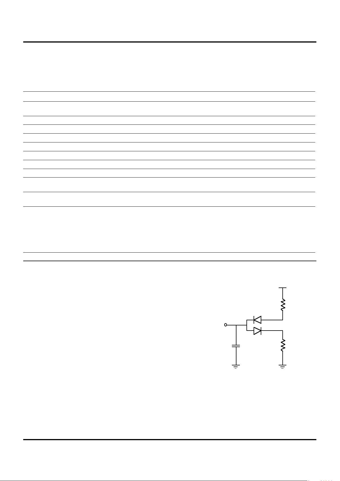
Positive current flows into the referenced pin (Figure 3).
Symbol Parameters Min Max Units Notes
V
CC
Power Supply
Voltage*
–0.3 +7 V
V
I
Input V oltage –0.3 V
CC
+0.3 V
V
I
Input V oltage –0.3 V
CC
+0.3 V 1
V
O
Output V oltage –0.3 13.2 V 2, 3
I
OH
Output Current High –10 mA 1 pin
I
OH
Output Current High –100 mA All total
I
OL
Output Current Low 20 mA 1 pin
I
OL
Output Current Low 200 mA All total
T
A
Operating
Temperature
†
T
STG
Storage
Temperature
–65 +150 C
Notes:
1. Port 2 open-drain
2. PWM open-drain outputs
3. Absolute maximum operating voltage 13.2V.
Absolute maximum momentary (non-operating) voltage is 16.0V.
* Voltage on all pins with respect to GND.
† See Ordering Information
Figure 3. Test Load Diagram
From Output
Under Test
RLL
VDD
RLH
150 pF

Z90102/90103/90104
40-Pin Low-Cost Digital Television Controller Zilog
8 DS97TEL1902
CAPACITANCE
T
A
= 25°C; VCC = GND = 0V; Freq =1.0 MHz; unmeasured pins to GND.
DC CHARACTERISTICS
T
A
= 0°C to +70°C; VCC = +4.5V to +5.5V; FOSC = 4 MHz
Parameter Max Units
Input capacitance 10 pF
Output
capacitance
20 pF
I/O capacitance 25 pF
AFCIN input
capacitance
10 pF
T
A
= 0°C to +70°C
Typical
Sym Parameter Min Max @ 25°C Units Conditions
V
IL
Input V oltage Low 0 0.2 V
CC
1.48 V
V
ILC
Input XTAL/Osc In Low 0.07 V
CC
0.98 V External Clock
Generator Driven
V
IH
Input V oltage High 0.7 V
CC
V
CC
3.0 V
V
IHC
Input XTAL/Osc In High 0.8 V
CC
V
CC
3.2 V External Clock
Generator Driven
V
HY
Schmitt Hysteresis 0.1 V
CC
0.8 V
V
PU
Maximum Pull-Up
Voltage
13.2 V 1, 2
V
OL
Output V oltage Low 0.4
0.4
0.16
0.19
V
V
IOL=1.00 mA
I
OL
=0.75 mA 1
V
00-01
AFC Level 01 In 0.45 V
CC
1.9 V
V
01-11
AFC Level 11 In 0.5 V
CC
0.75 V
CC
3.12 V
V
OH
Output V oltage High VCC –0.4 4.75 V IOH=–0.75 mA
I
IR
Reset Input Current –80 –46 mAVRL=0
V
II
L
Input Leakage –3.0 3.0 0.01 mA0V, V
CC
I
OL
Tristate Leakage –3.0 3.0 0.02 mA0V, V
CC
I
CC
I
CC1
I
CC2
Supply Current 20
6
10
13.2
3.2
2.0
mA
mA
mA
All inputs at rail &
outputs floating
Notes:
1. PWM open-drain
2. Recommended operating voltage 12V with maximum positive
tolerance 10%, i.e., 13.2V.

Z90102/90103/90104
Zilog 40-Pin Low-Cost Digital Television Controller
DS97TEL1902 9
1
AC CHARACTERISTICS
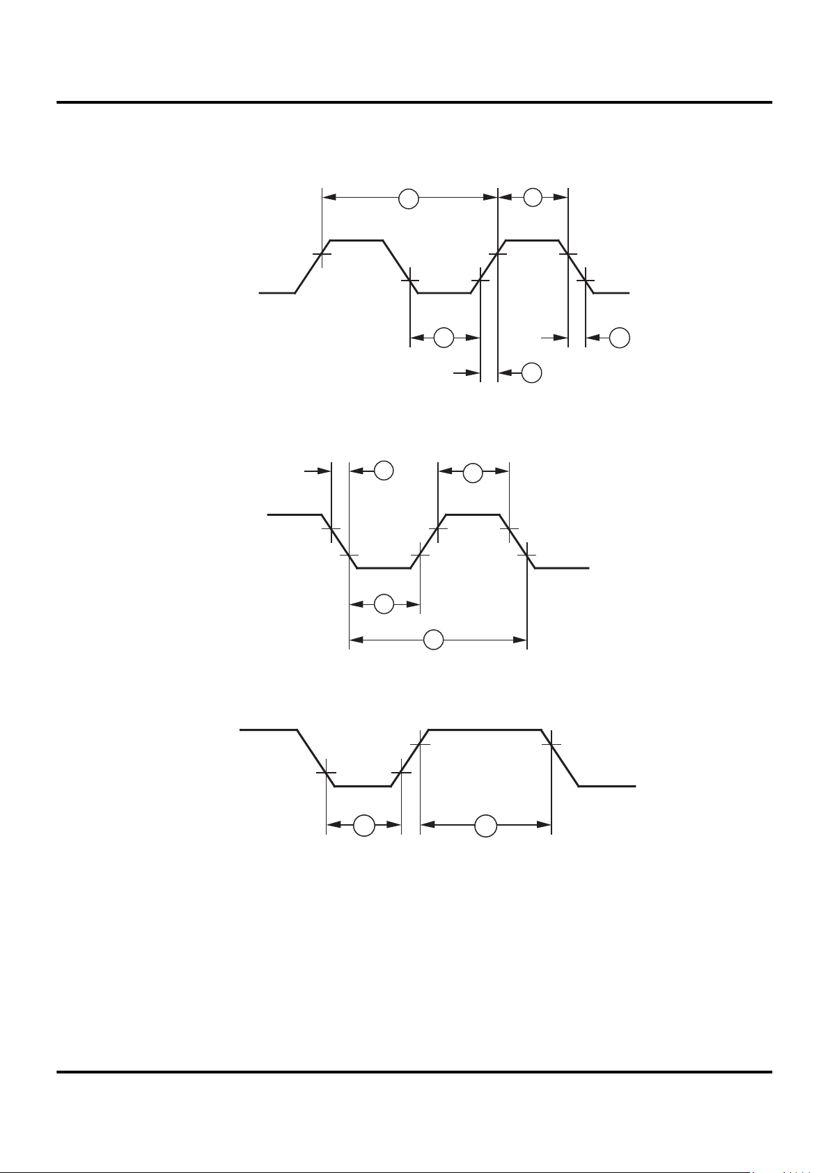
Timing Diagrams
Figure 4. External Clock
XTAL1
2
2
1
3
3
Figure 5. Counter Timer
TIN
7
5
4
6
Figure 6. Interrupt Request
IRQN
8 9

Z90102/90103/90104
40-Pin Low-Cost Digital Television Controller Zilog
10 DS97TEL1902
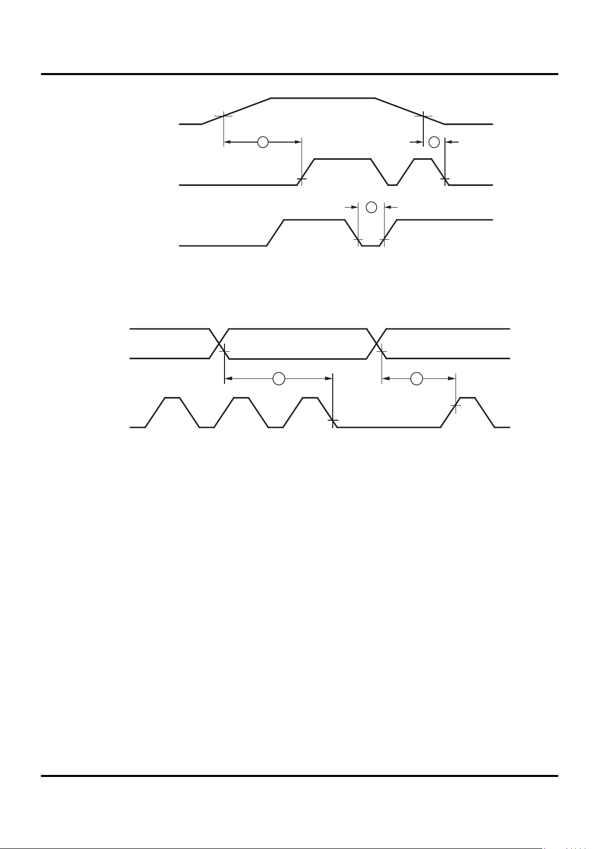
Figure 7. Power-On Reset
External /RESET
10
11
12
Internal /RESET
VCC
Figure 8. On-Screen Display
HSYNC
1413
OSC2

Z90102/90103/90104
Zilog 40-Pin Low-Cost Digital Television Controller
DS97TEL1902 11
1
AC CHARACTERISTICS
T
A
= 0° C to +70° C; VCC = +4.5V to +5.5V; F
OSC
= 4 MHz
No Symbol Parameter Min Max Unit
1 TpC Input Clock Period 250 1000 ns
2 TrC,TfC Clock Input Rise and Fall 15 ns
3 TwC Input Clock Width 125 ns
4 TwTinL Timer Input Low Width 70 ns
5 TwTinH Timer Input High Width 3TpC
6 TpTin Timer Input Period 8TpC
7 TrTin,TfTin Timer Input Rise and Fall 100 ns
8a TwIL Int Req Input Low 70 ns
8b TwIL 3TpC
9 TwIH Int Request Input High 3TpC
10 TdPOR Power On Reset Delay 25 100 ms
11 TdLVIRES Low Voltage Detect to 200 ns
Internal RESET
Condition
12 TwRES Reset Minimum Width 5TpC
13 TdHsOI HSYNC Start to VOSC
Stop
2TpV 3TpV
14 TdHsOh HSYNC End to VOSC
Start
1TpV
15 TdWDT WDT Refresh Time 12 ms
Notes:
Refer to DC Characteristics for details on switching levels.
 Loading...