


1
0 °
P
RELIMINARY
C
USTOMER
P
ROCUREMENT
S
PECIFICATION
FEATURES
ROM
Device
Z89332 24 640 8 4.5 to 5.5V
Note: *General-Purpose
■
42-Pin SDIP and 48-Pin Ceramic Packages with
42- to 48-Pin Adapter Socket
C to +70 ° C Temperature Range
■
(KW)
RAM*
(Words)
PWM
(8-Bit)
Voltage
Range
GENERAL DESCRIPTION
The Z89332 Digital Television Controller is designed to
provide complete audio and video control of television receivers, video recorders, and advanced on-screen display
facilities. The television controller features a Z89C00 RISC
processor core that controls the on-board peripheral functions and registers using the standard processor instruction set.
Character attributes can be controlled through two modes:
the on-screen display Character-Control Mode and the
Closed-Caption Mode. The Character-Control Mode provides access to the full set of attribute controls, allowing the
modification of attributes on a character-by-character basis. The insertion of control characters permits direction of
other character attributes. Closed-caption text can be decoded directly from the composite video signal and displayed on-screen with the assistance of the processor's
digital signal processing (DSP) capabilities.
The fully customized 512 character set, formatted in two
256 character banks, can be displayed with a host of display attributes that include underlining, italics, blinking,
eight foreground/background colors, character position offset delay, and background transparency.
Z89332
D
IGITAL
■
Fully Customized Character Set
■
Character-Control and Closed-Caption Modes
Keypad User Control
■
■
TV Tuner Serial Interface
■
Direct Video Signals
■
Speed: 12 MHz
Serial interfacing with the television tuner is provided
through the tuner serial port. Other serial devices, such as
digital channel tunning adjustments, may be accessed
through the industry-standard I
User control can be monitored through the keypad scanning port, or the 16-bit remote control capture register. Receiver functions such as color and volume can be directly
controlled by eight 8-bit pulse width modulated ports.
Notes:
All Signals with a preceding front slash, "/", are active Low,
e.g.: B//W (WORD is active Low); /B/W (BYTE is active
Low, only).
Power connections follow conventional descriptions below:
Connection Circuit Device
T
ELEVISION
Power V
Ground GND V
C
ONTROLLER
2
C port.
CC
V
DD
SS
1
CP96TEL0607
P R E L I M I N A R Y
1-1
Z89332
Digital Television Controller
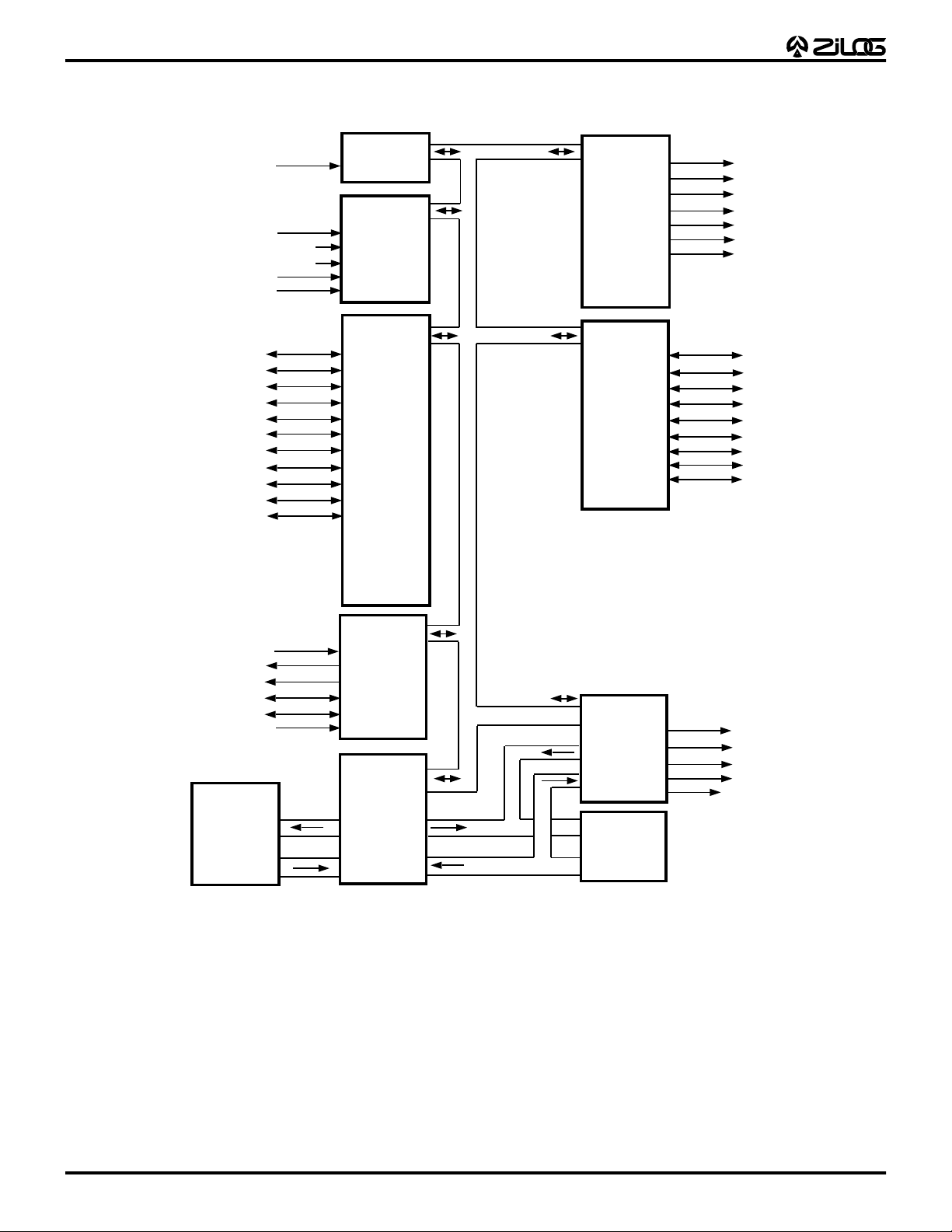
GENERAL DESCRIPTION (Continued)
Port 17
Port 00
Capture
IRIN
ADC
ADC0
ADC1
ADC2
ADC3
ADC4
Port 0
Port 00
Port 01
Port 02
Port 03
Port 04
Port 05
Port 06
Port 07
Port 08
Port 09
Port 0F
PWM
PWM1
PWM2
PWM3
PWM4
PWM5
PWM9
PWM10
Port1
Port 10
Port 11
Port 12
Port 13
Port 14
Port 15
Port 16
Port 17
Port 18
RAM
640 x 16
Address
Data
Control
XTAL1
XTAL2
LPF
HSYNC
VSYNC
/Reset
CPU
Register Addr/Data
HALFBLNK
ROM Addr
ROM Data
Figure 1. Functional Block Diagram
OSD
VBLANK
ROM
24K x 16
V1
V2
V3
Port0F
1-2
P R E L I M I N A R Y
CP96TEL0607
1
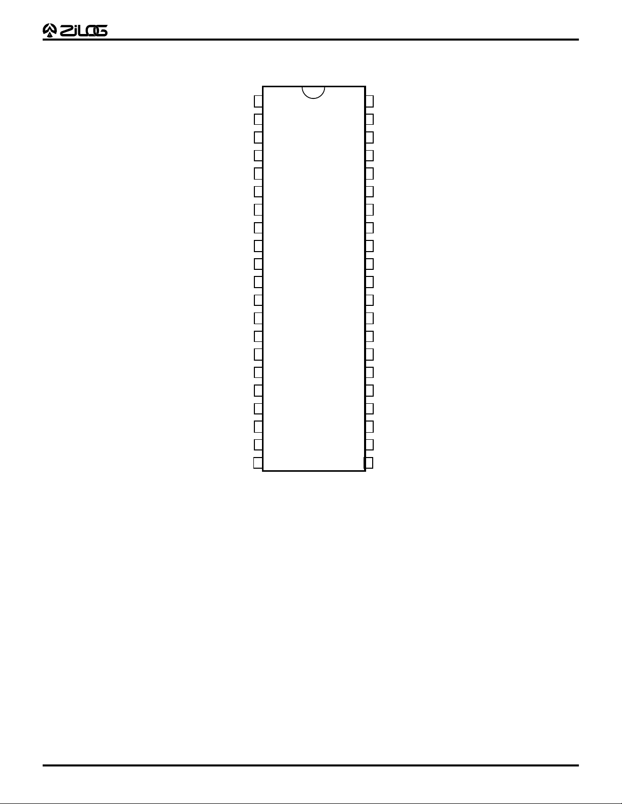
PIN DESCRIPTION
Z89332
Digital Television Controller
PWM10
PWM9
PWM5
PWM4
PWM3
PWM2
PWM1
Port03
Port04/ADC4
Port05/ADC3
Port00/ADC2
Port17/ADC1
GND
Port10/R<0>
Port06/Counter
Port18/G<0>
Port13/G<1> HSync
1
2
3
4
5
6
7
8
9
10
11
12
13
15
16
17
Z89332
Shrink
DIP
42
41
40
39
38
37
36
35
34
33
32
31
30
2914
28
27
26
Port12/I2MSD
P11/I2MSC
Port02/I2SSD
Port01/I2SSC
Port09
Port08/R<1>
IRIN
Port07/CSync
Vcc
/Reset
XTAL2
XTAL1
ANGND
LPF
CVI/ADC0
VSync
Port14/B<0>
Port15/B<1>
Port16/SCLK
Port0F/HalfBlnk V3
18
19
20
21
25
24
23
22
VBlank
V1
V2
Figure 2. 42-Pin Shrink DIP and 48-Pin Ceramic Pin Configurations
with 42- to 48-Pin Adapter Footprint
CP96TEL0607
P R E L I M I N A R Y
1-3

Z89332
Digital Television Controller
Table 1. 42-Pin SDIP Pin Identification
Name Function Z89332 Direction Reset Notes
V
CC
+ 5 Volts 34 PWR –
GND 0 V olts 13, 30 PWR –
IRIN Infrared Remote Capture
36 I I
Input
ADC[4:0] 4-Bit A/D Converter Input 9, 10, 11, 12, 28 AI I
PWM10, PWM9 14-Bit Pulse Width
1, 2 O O
Modulator Output
PWM[5:1] 8-Bit Pulse Width Modulator
3, 4, 5, 6, 7 OD/O* O
Output
Port0[F:0] Bit Programmable
Input/Output Ports
21, -, -, -, -, -, 38, 37,
35, -, -, 15, 8, 40, 39,
B I [1]
11
Port1[8:0] Bit Programmable
Input/Output Ports
SCL
SCD
2
I
C Clock I/O
2
C Data I/O
I
16, 12, 20, 19, 18, 17,
42, 41, 14
39 or 41 BOD [2]
40 or 42 BOD [3]
BI
XTAL1 Crystal Oscillator Input 31 AI I
XTAL2 Crystal Oscillator Output 32 AO O
LPF Loop Filter 29 AB O
HSYNC H_SYNC 26 B I
VSYNC V_SYNC 27 B I
/Reset Device Reset 33 I I
V[3:1] OSD Video Output T ypically
22, 23, 24 O O
Drive B, G, and R Outputs
Blank OSD Blank Output 25 O O
HalfBlank OSD Half-Blank Outpu 21 O [4]
RGB Digital
Outputs
R[1:0], G[1:0], and B[1:0]
Outputs of the RGB Matrix
37, 14, 17, 16, 19, 18 O [5]
SCLK Internal Processor SCLK 20 O [6]
Notes:
1) Port 0 [E:A] is not available on the 42-pin SDIP version.
2) SCL I/O pin is shared with Port 0 or Port 11.
3) SCD I/O pin is shared with Port 02 or Port 12.
4) Half Blank output is a function shared with Port 0F.
5) Digital RGB outputs and the internal SCLK are shared with Port 1 [5:0].
6) Internal processor SCLK is shared with Port 16.
* PWM outputs are push/pull in Revision Z89332EA and later.
1-4
P R E L I M I N A R Y
CP96TEL0607

1
V1, V2, V3 ANALOG OUTPUT
Specifications V
V
= 5.25V
CC
Output Voltage Bit = 11 4.2V ± 0.4V
Setting Time 70% of DC Level, 10 pF Load < 50 nsec
V
= 4.75V
CC
Output Voltage Bit = 11 3.6V ± 0.4V
Setting Time 70% of DC Level, 10 pF Load < 50 nsec
= 5.25V and V
CC
= 4.75V
CC
Condition Limit
Bit = 10 45% – 0.15V to 55% of actual data = 11 value
Bit = 01 0.60 V ± 0.4V
Bit = 00 74% to 89% of actual data = 11 value
Condition Limit
Bit = 10 45% – 0.15V to 55% of actual data = 11 value
Bit = 01 0.60V ± 0.4V
Bit = 00 74% to 89% of actual data = 11 value
Z89332
Digital Television Controller
Z893XX
10 pF
47 pF
10 MΩ
Figure 3. 32K Oscillator Recommended Circuit
32.768kHz
68 KΩ
Z893XX
510 Ω
47 µF
XTAL1
XTAL2
0.1 µF
CP96TEL0607
Figure 4. Recommended Low Pass Filter Circuit
P R E L I M I N A R Y
1-5

Z89332
Digital Television Controller
ABSOLUTE MAXIMUM RATINGS
Symbol Parameter Min Max Units Conditions
V
CC
V
ID
V
IA
V
O
V
O
V
O
I
OH
I
OH
I
OL
I
Output Current Low 200 mA All Pins
OL
T
A
T
A
Power Supply Voltage 0 7 V
Input V oltage –0.3 V
Input V oltage –0.3 V
Output V oltage –0.3 V
Output V oltage –0.3 V
+0.3 V Digital Inputs
CC
+0.3 V Analog Inputs (A/D0...A/D4)
CC
+0.3 V All Push-Pull Digital Output
CC
+8 Open-Drain PWM Outputs
CC
(PWM1...PWM8)
Output V oltage –0.3 V
+0.3 V Push/Pull PWM Outputs
CC
(PWM1...PWM8) = Z89332EA
and Later Revisions
Output Current High –10 mA One Pin
Output Current High –100 mA All Pins
Output Current Low 20 mA One Pin
Operating Temperature 0 70 ° C
Storage Temperature –65 150 ° C
DC CHARACTERISTICS
T
= 0 ° C to + 70 ° C; V
A
Symbol P arameter Min Max Typical Units Conditions
V
V
V
PU
V
OL
V
OH
V
V
XH
V
HY
I
IR
I
IL
I
CC
I
ADC
I
ADC
IL
IH
XL
Input V oltage Low 0 0.2 V
Input V oltage High 0.7 V
Max. Pull-Up Voltage V
Output Voltage Low 0.4 0.16 V @ IOL = 1 mA
Output V oltage High VCC –0.4 4.75 V @ IOL = 0.75 mA
Input Voltage XTAL1 Low 0.3 V
Input Voltage XTAL1 High VCC –2.0 3.5 V Generator Driven
Schmitt Hysteresis 3.0 0.75 0.5 V On XTAL1 Input Pin
Reset Input Current 150 90 µAV
Input Leakage –3.0 3.0 0.01 µA @ 0V and V
Supply Current 100 60 mA
Input Current 0.5 mA AE Revision
Input Current 10 µA CC,CA,EA & Later Rev.
Notes:
A) The Z89332 should not be operated for extended periods with the crystal oscillator disconnected, except in the defined
power-down modes. In the event that the Z89332 is operated with the oscillator disconnected, the device may draw higher
than typical current.
B) Each line of the on-screen display can consist of any number of characters, up to a maximum of 30 characters.
= 4.5V to + 5.5V; F
CC
CC
= 32.768 KHz
OSC
V
CC
+0.3 V All Pins
CC
CC
CC
0.4 V
3.6 V
1.0 V External Clock
= 0V
RL
CC
1-6
P R E L I M I N A R Y
CP96TEL0607

1
AC CHARACTERISTICS
= 0°C to + 70°C; VCC = 4.5V to 5.5V; F
T
A
= 32.768 KHz
OSC
Z89332
Digital Television Controller
Symbol Parameter Min Max Typical Units
TPC Input Clock Period 16 100 32 µS
T
C,TFC Clock Input Rise and Fall 12 µS
R
T
POR Power-On Reset Delay 0.8 1.2 Sec
D
AC CHARACTERISTICS
TA = 0°C to + 70°C; VCC = 4.5V to 5.5V; F
Symbol Parameter Min Max Typical Units
T
RES Power-On Reset Min. Width 5 TPC µS
W
T
DHS
T
DVS
T
DES
T
DOS
T
WHVS
Note:
All timing of the I
Time Delay Between Leading Edge of V_Sync and H_Sync in Even Field –12 +12 0 µS
Time Delay Between Leading Edge of H_Sync in Odd Field 20 44 32 µS
2
C bus interface are defined by related specifications of the I2C bus interface.
H_Sync Incoming Signal Width 5.5 12.5 11 µS
V_Sync Incoming Signal Width 0.15 1.5 1.0 mS
H_Sync/V_Sync Edge Width 2.0 0.5 µS
= 32.768 KHz
OSC
CP96TEL0607 P R E L I M I N A R Y 1-7

Z89332
Digital Television Controller
1-8 P R E L I M I N A R Y CP96TEL0607
 Loading...