


PRELIMINARY
FEATURES
■ Part ROM RAM Speed
Number (Word) (Word) (MHz)
Z89319 0 0 12
Z89319
CPS5TEL0800
P
RELIMINARY
C
USTOMER PROCUREMENT SPECIFICATION
Z89319
DIGITAL TELEVISION CONTROLLER
IN-CIRCUIT EMULATOR (ICE) DEVICE
■ Direct Closed Caption Decoding
■ 124-Pin Grid Array (PGA) Package
■ 4.5- to 5.5-Volt Operating Range
■ Z89C00 RISC Processor Core
■ 0°C to +70°C Temperature Range
GENERAL DESCRIPTION
The Z89319 is a ROMless ICE chip version of the Z89300
family of Zilog's Digital Television Controllers designed for
use in emulators and development boards to provide
complete audio and video control of television receivers,
video recorders, and advanced on-screen display facilities.
The powerful Z89C00 RISC processor core allows users to
control on-board peripheral functions and registers using
the standard processor instruction set.
In closed caption mode, text can be decoded directly from
the composite video signal and displayed on the screen
with assistance from the processor's digital signal
processing capabilities. The character representation in
this mode allows for a simple attribute control through the
insertion of control characters.
The character control mode provides access to the full set
of attribute controls. The modification of attributes is allowed
on a character-by-character basis. The insertion of control
characters permits direction of other character attributes.
■ TV Tuner Serial Interface
■ Customized Character Set
■ Character Control Mode
■ Directly Controlled Receiver Functions
Serial interfacing with the television tuner is provided
through the tuner serial port. Digital channel tuning
adjustments may be accessed through the industrystandard I2C port.
Additional hardware provides the capability to display two
to three times normal size characters. The smoothing logic
contained in the on-screen display circuit improves the
appearance of larger fonts. Special circuitry can be
activated to improve the visibiity of text by adding a rightsided shadow effect to the characters.
Receiver functions such as color and volume can be
directly controlled by six 8-bit pulse width modulated
ports.
Notes:
All Signals with a preceding front slash, "/", are active Low, e.g.:
B//W (WORD is active Low); /B/W (BYTE is active Low, only).
Power connections follow conventional descriptions below:
Display attributes, including underlining, italics, blinking,
eight foreground/background colors, character position
offset delay, and background transparency, are made
possible through a fully customized 512 character set,
formatted in two 256 character banks.
CP95TEL0800 (6/95)
Connection Circuit Device
Power V
Ground GND V
CC
V
DD
SS
1
PRELIMINARY
GENERAL DESCRIPTION (Continued)
Z89319
CP95TEL0800
CVI
PWM6
Port 17
Port 00
Port 05
Port 04
Capture
IRIN
ADC
ADC0
ADC1
ADC2
ADC3
ADC4
ADC5
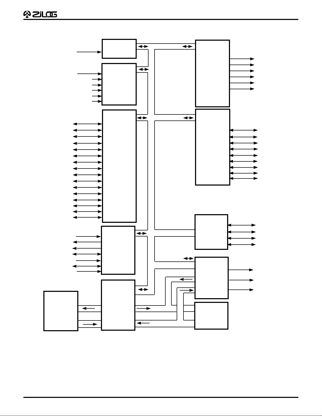
Port 0
Port 00
Port 01
Port 02
Port 03
Port 04
Port 05
Port 06
Port 07
Port 08
Port 09
Port 0A
Port 0B
Port 0C
Port 0D
Port 0E
Port 0F
Control
XTAL1
XTAL2
LPF
HSYNC
HSYNC2
VSYNC
/Reset
Register Addr/Data
PWM
PWM1
PWM2
PWM3
PWM4
PWM5
PWM6
Port1
Port 10
Port 11
Port 12
Port 13
Port 14
Port 15
Port 16
Port 17
Port 18
I2C
SCL/MSCL2
SCD/MSCD2
MSCL1
MSCD1
OSD
V1(R)
Port 01/11
Port 02/12
CPU
V2(G)
V3(B)
RAM
1K x 16
Address
Data
ROM Addr
ROM
32K x 16
ROM Data
Functional Block Diagram
2
PRELIMINARY
3
Z89319
CPS5TEL0800
P03
P01
VCC
GND
ADDRESS12
ADDRESS11
P02
ADDRESS10
ADDRESS9
ADDRESS8
ADDRESS7
ADDRESS6
CVI/ADC0
ADDRESS5
ADDRESS4
VCC
GND
ADDRESS3
LPF
ADDRESS2
ADDRESS1
ADDRESS0
R/W
ANGNDF
SYS_CLK
EA0
EA1
EA2
ADC5
P04/ADC4
P06/CNTR
ADDRESS1
P07/CSYNC
ADDRESS14VCC
P0D
P09
P19
P0A
P0B
P0C
INT_BUS15
IRIN
INT_BUS14
INT_BUS13
P16/SCLK
P15/B<1>
P14/B<0>
GND
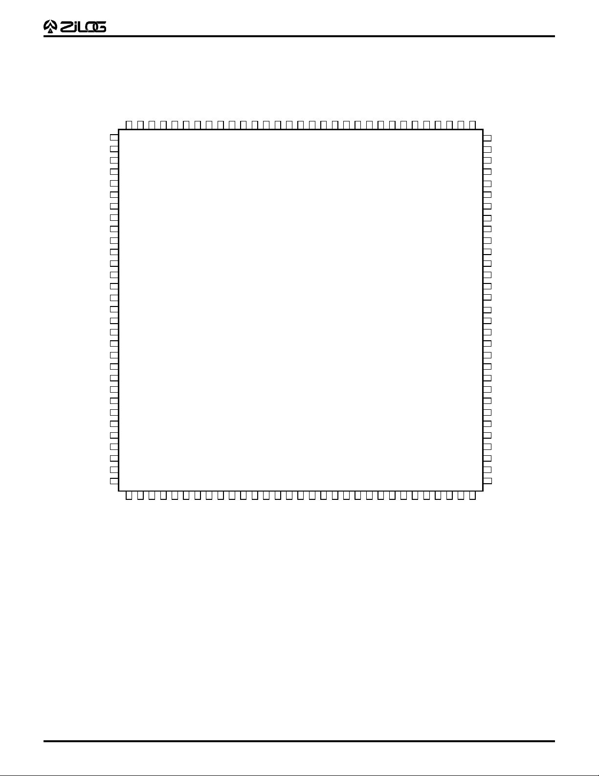
Z89319
124-Pin PGA
IE
P13/G<1>
P18/G<0>
VCC
P08/R<1>
INT_BUS12
P10/R<0>
INT_BUS11
PWM6
INT_BUS10
PWM5
PWM4
PWM3
GND
PWM2
VCC
DATA0
DATA1
DATA2
PWM1
DATA3
DATA4
DATA5
DATA6
SINGLE_STEP
ANGNDX
STOPWDT
DATA7
DATA8
DATA9
_ROMLESS
VCC/VDD
_PABUS
DATA12
DATA13
DATA14
DATA10
GND
DATA11
DATA15
GND
INT_BUS9
XTAL2
XTAL1
GND
P05/ADC3
INT_BUS0
P17/ADC1
P001/ADC2
ANGND
INT_BUS1
ANVCC
INT_BUS2
P0F/HB
INT_BUS3
V3(B)
VCC
V2(G)
V1(R)
GND
124-Pin PGA Configuration
BLANK
HSYNC
VSYNC
INT_BUS4
INT_BUS5
P11/I2MSC2
P12/I2MSD2
P0E
INT_BUS6
VCC
I2MSD1
INT_BUS7
I2MSC1
INT_BUS8
/RESET
3

PIN DESCRIPTION
PRELIMINARY
Z89319
CP95TEL0800
N
M
L
K
J
H
Z89319
13121110987654321
124-Pin PGA Configuration
G
F
E
D
C
B
A
4

V1, V2, V3 ANALOG OUTPUT
Specifications VCC = 5.25 V
VCC = 5.25 V Condition Limit
Output Voltage Bit = 11 4.30 V ± 0.3 V
Setting Time 70% of DC Level, < 50 ns
V1, V2, V3 ANALOG OUTPUT
Specifications VCC = 4.75 V
VCC = 4.75 V Condition Limit
PRELIMINARY
Bit = 10 3.10 V ± 0.25 V
Bit = 01 1.90 V ± 0.20 V
Bit = 00 0 V ± 0.75 V
10pf Load
Z89319
CPS5TEL0800
Output Voltage Bit = 11 3.90 V ± 0.30 V
Bit = 10 2.80 V ± 0.25 V
Bit = 01 1.70 V ± 0.20 V
Bit = 00 0 V ± 0.65 V
Setting Time 70% of DC Level, < 50 ns
10pf Load
Z893XX
68pF
560pF
10 Mohm
32.768k
27k
XTAL1
XTAL2
32K Oscillator Recommended Circuit
5

PRELIMINARY
ABSOLUTE MAXIMUM RATINGS
Symbol Parameter Min Max Units Conditions
Z89319
CP95TEL0800
V
CC
V
ID
V
IA
V
O
I
OH
I
OH
I
OL
I
OL
T
A
T
A
Notes:
a) 1 mA max. when output pad impedance is 600 Ω.
b) 1 mA max. when output pad impedance is 600 Ω.
Power Supply Voltage 0 7 V
Input Voltage –0.3 V
Input Voltage –0.3 V
Output Voltage –0.3 V
Output Current High –10/–1
+0.3 V Digital Inputs
CC
+0.3 V Analog Inputs (A/D0...A/D4)
CC
+0.3 V All Push-Pull Digital Output
CC
a
mA One Pin
Output Current High –100 mA All Pins
Output Current Low 20/1
b
mA One Pin
Output Current Low 200 mA All Pins
Operating Temperature 0 70 °C
Storage Temperature –65 150 °C
DC CHARACTERISTICS
TA = 0°C to + 70°C; VCC = 4.5 V to + 5.5 V; F
Symbol Parameter Min Max Typical Units Conditions
V
IL
V
IH
Input Voltage Low 0 0.2 V
Input Voltage High 0.6 V
CC
= 32.768 KHz
OSC
CC
V
CC
0.4 V
3.6 V
V
V
V
V
V
I
I
I
I
I
OL
OH
XL
XH
HY
IR
IL
CC
CC1
CC2
Output Voltage Low 0.4 0.16 V @ IOL = 1 mA
Output Voltage High V
Input Voltage XTAL1 Low 0.3 V
–0.9 4.75 V @ IOL = 0.75 mA
CC
CC
1.0 V External Clock
Input Voltage XTAL1 High VCC –2.0 3.5 V Generator Driven
Schmitt Hysteresis 3.0 0.75 0.5 V On XTAL1 Input Pin
Reset Input Current 150 90 µAV
RL
Input Leakage –3.0 3.0 0.01 µA @ 0 V and V
Supply Current 100 60 mA
Supply Current 300 100 µA Sleep Mode @ 32 KHz
Supply Current 40 5 µA Stop Mode
= 0 V
CC
6

PRELIMINARY
Z89319
CPS5TEL0800
AC CHARACTERISTICS
TA = 0°C to + 70°C; VCC = 4.5 V to 5.5 V; F
Symbol Parameter Min Max Typical Units Note
TPC Input Clock Period 16 100 32 µS
TRC,TFC Clock Input Rise and Fall 12 µS
TDPOR Power On Reset Delay 0.8 1.2 s Depends on Crystal
= 32.768 KHz
OSC
AC CHARACTERISTICS*
TA = 0°C to + 70°C; VCC = 4.5 V to 5.5 V; F
Symbol Parameter Min Max Typical Units
TWRES Power-On Reset Min. Width 5TPC µS
TDH
TDV
TDE
S
S
S
H_Sync Incoming Signal Width 5.5 12.5 11 µS
V_Sync Incoming Signal Width 0.15 1.5 1.0 mS
Time Delay Between Leading Edge –12 +12 0 µS
of V_Sync and H_Sync in Even Field
= 32.768 KHz
OSC
TDO
S
Time Delay Between Leading Edge 20 44 32 µS
of H_Sync in Odd Field
TWHV
S
Notes:
All timing of the I2C bus interface are defined by related specifications of
the I2C bus interface.
H_Sync/V_Sync Edge Width 2.0 0.5 µS
7
 Loading...