

FEATURES
Z89314/318
CPS95TV0403
CUSTOMER PROCUREMENT SPECIFICATION
Z89314/318
DIGITAL TELEVISION CONTROLLER
■ Part Z8 ROM Z8 RAM* Speed
Number (Kbyte) (Kbyte) (MHz)
Z89314 16 512 12
Z89318 10 512 12
*General-Purpose
■ 40-Pin DIP Package
■ 4.5- to 5.0-Volt Operating Range
■ Z89C00 RISC Processor Core
GENERAL DESCRIPTION
The Z89314/318 are members of Zilog's family of Digital
Television Controllers designed to provide complete audio
and video control of television receivers, video recorders,
and advanced on-screen display facilities.
The powerful Z89C00 RISC processor core allows users to
control on-board peripheral functions and registers using
the standard processor instruction set.
In closed caption mode, text can be decoded directly from
the composite video signal and displayed on the screen
with assistance from the processor's digital signal
processing capabilities. The character representation in
this mode allows for a simple attribute control through the
insertion of control characters.
The character control mode provides access to the full set
of attribute controls. The modification of attributes is allowed
on a character-by-character basis. The insertion of control
characters permits direction of other character attributes.
■ 0°C to +70°C Temperature Range
■ Direct Closed Caption Decoding
■ TV Tuner Serial Interface
■ Customized Character Set
■ Character Control Mode
■ Directly Controlled Receiver Functions
Serial interfacing with the television tuner is provided
through the tuner serial port. This version of the Z89300
series does not offer I2C capability
Additional hardware provides the capability to display two
to three times normal size characters. The smoothing logic
contained in the on-screen display circuit improves the
appearance of larger fonts. Fringing circuitry can be
activated to improve the visibiity of text by surrounding the
character lines with a one-pixel border.
Receiver functions such as color and volume can be
directly controlled by eight 8-bit pulse width modulated
ports.
Notes:
All Signals with a preceding front slash, "/", are active Low, e.g.:
B//W (WORD is active Low); /B/W (BYTE is active Low, only).
Power connections follow conventional descriptions below:
Display attributes include underlining, italics, blinking,
eight foreground/background colors, character position
offset delay, and background transparency are made
possible through a fully customized 512 character set,
formatted in two 256 character banks.
CPS95TV0403 (8/95)
Connection Circuit Device
Power V
Ground GND V
CC
V
DD
SS
1
GENERAL DESCRIPTION (Continued)
Z89314/318
CPS95TV0403
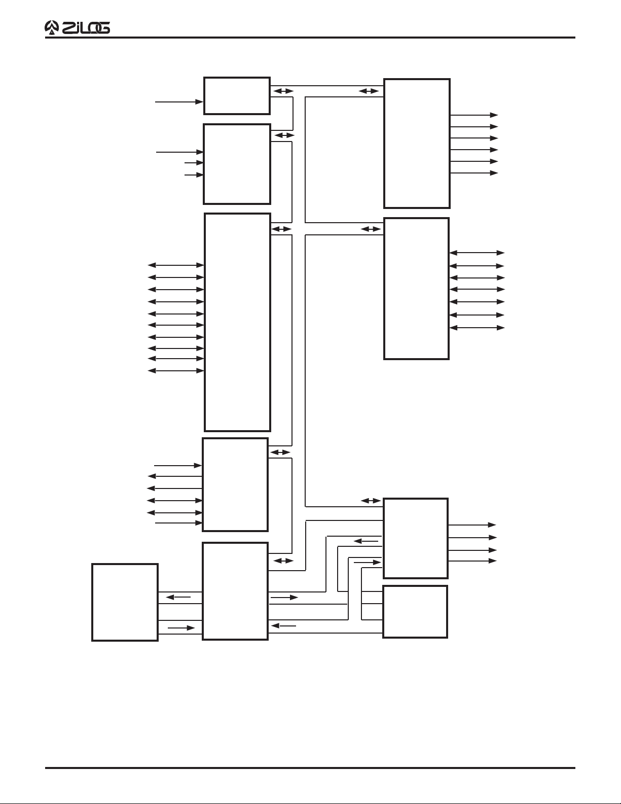
Port 17
Port 00
Capture
IRIN
ADC
ADC0
ADC1
ADC2
Port 0
Port 00
Port 01
Port 02
Port 03
Port 04
Port 05
Port 06
Port 07
Port 08
Port 09
PWM
PWM1
PWM2
PWM3
PWM4
PWM5
PWM6
Port1
Port 10
Port 11
Port 12
Port 13
Port 14
Port 15
Port 16
RAM
512 x 16
Address
Data
Control
XTAL1
XTAL2
LPF
HSYNC
VSYNC
/Reset
CPU
Register Addr/Data
ROM Addr
ROM Data
Functional Block Diagram
OSD
V1
V2
V3
BLANK
ROM
16K x 16
Z89314
10K x 16
Z89318
2
PIN DESCRIPTION
Z89314/318
CPS95TV0403
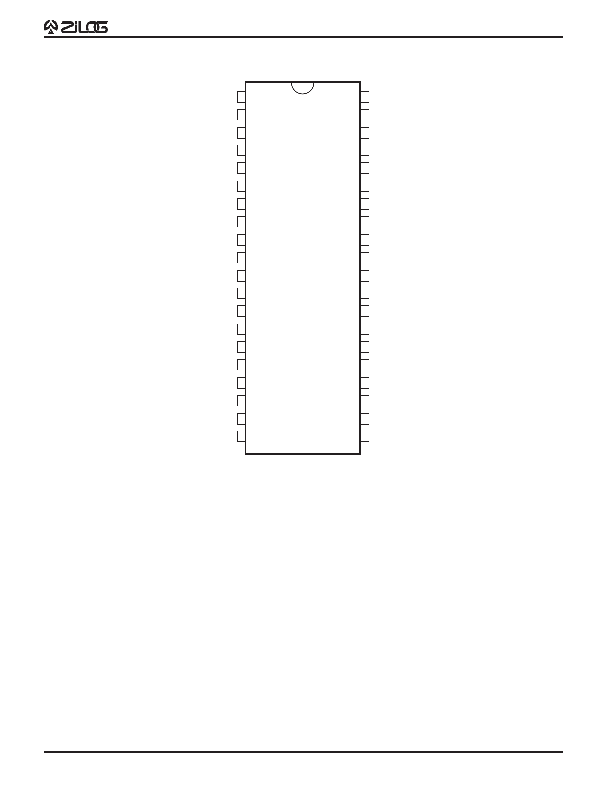
N/A PWM9
IRIN
Port 18
Port 00/ADC2
Port 01
Port 02
Port 03
Port 04
Port 05
Port 06
Port 07
Port 08
Port 09
Port 10
Port 11
Port 12
Port 13
Port 14
Port 15
Port 16
1
2
3
4
5
6
7
8
9
10
11
12
13
14
15
16
17
18
19
20
Z89314
Z89318
40
39
38
37
36
35
34
33
32
31
30
29
28
27
26
25
24
23
22
21
PWM6
PWM5
PWM4
PWM3
PWM2
PWM1
CVI/ADC0
LPF
XTAL2
GND
XTAL1
VCC
/Reset
Port 17/ADC1
VBlank
V1
V2
V3
VSync
HSync
40-Pin DIP Configuration
3

Z89314/318
CPS95TV0403
PIN DESCRIPTION (Continued)
Z89314/318
Pin Z89314 Configuration
Name Function 40-Pin Direction Reset
V
CC
+5 V 29,– PWR –
GND 0 V 31,– PWR –
IRIN Infrared Remote Capture Input 2 I I
ADC[5:0] 4-Bit Analog to Digital Converter –,–,–,4,27,34 AI I
Input
PWM[8:1]a8-Bit Pulse Width Modulator –,–,40,39,38 OD O
Output 37,36,35
Port0[F:0]bBit Programmable Input/Output Ports –,–,–,–,–,–, B I
13,12,11
10,9,8,7,6,5,4
Port1[9:0]aBit Programmable Input/Output Ports –,3,27,20, B I
19,18,17,
16,15,14
XTAL1 Crystal Oscillator Input 30 AI I
XTAL2 Crystal Oscillator Output 32 AO O
LPF Loop Filter 33 AB O
HSYNC H_Sync 21 B I
VSYNC V_Sync 22 B I
/RESET Device Reset 28 I I
V[3:1] OSD Video Output 23,24,25 O O
(Typically Drive B, G, and R Outputs)
Blank OSD Blank Output 26 O O
Half Blank OSD Half Blank Output N/A O
e
SCLK
Notes:
a) PWM [8,7] is not available on the 40-pin DIP version.
b) Port0 [F:A] is not available on the 40-pin DIP version.
c) Port19 is not available on the 40-pin DIP version.
d) Half Blank output is a function shared with Port0F.
Half Blank output is not available on the 40-pin DIP version.
e) Internal processor SCLK is shared with Port16.
Internal Processor SCLK 20 O
4

68pF
Z89314/318
CPS95TV0403
Z893XX
XTAL1
560pF
10 Mohm
32K Oscillator Recommended Circuit
32.768k
XTAL2
27k
5

ABSOLUTE MAXIMUM RATINGS
Symbol Parameter Min Max Units Conditions
Z89314/318
CPS95TV0403
V
CC
V
ID
V
IA
V
O
V
O
Power Supply Voltage 0 7 V
Input Voltage –0.3 V
Input Voltage –0.3 V
Output Voltage –0.3 V
Output Voltage –0.3 V
+0.3 V Digital Inputs
CC
+0.3 V Analog Inputs (A/D0...A/D4)
CC
+0.3 V All Push-Pull Digital Output
CC
+8.0 V Open-Drain PWM Outputs
CC
(PWM1...PWM8)
I
OH
I
OH
I
OL
I
OL
T
A
T
A
Output Current High –10 mA One Pin
Output Current High –100 mA All Pins
Output Current Low 20 mA One Pin
Output Current Low 200 mA All Pins
Operating Temperature 0 70 °C
Storage Temperature –65 150 °C
DC CHARACTERISTICS
T
= 0°C to + 70°C; V
A
Symbol Parameter Min Max Typical Units Conditions
V
V
V
V
V
V
V
V
I
IR
I
IL
I
CC
I
CC1E
I
CC1
I
CC2
IL
IH
PU
OL
3
OL
XL
XH
1
HY
2
2
Input Voltage Low 0 0.2 V
Input Voltage High 0.6 V
Max. Pull-Up Voltage 12 V PWM0...PWM8 Only
Output Voltage Low 0.4 0.16 V @ IOL = 1 mA
Output Voltage High V
Input Voltage XTAL1 Low 0.3 V
Input Voltage XTAL1 High VCC –2.0 3.5 V Generator Driven
Schmitt Hysteresis 3.0 0.75 0.5 V On XTAL1 Input Pin
Reset Input Current 150 90 µAV
Input Leakage –3.0 3.0 0.01 µA @ 0 V and V
Supply Current 100 60 mA
Supply Current of the OTP 700 300 µA Sleep Mode @ 32 KHz
Supply Current 300 100 µA Sleep Mode @ 32 KHz
Supply Current 40 5 µA Sleep Mode
= 4.5 V to + 5.5 V; F
CC
–0.9 4.75 V @ IOL = 0.75 mA
CC
CC
= 32.768 KHz
OSC
CC
V
CC
CC
0.4 V
3.6 V
1.0 V External Clock
= 0 V
RL
CC
Notes:
1. Not in the EOS.
2. Z89314 is not an OTP.
3. Labeled incorrect.
6

AC CHARACTERISTICS
T
= 0°C to + 70°C; V
A
= 4.5 V to 5.5 V; F
CC
= 32.768 KHz
OSC
Symbol Parameter Min Max Typical Units
TPC Input Clock Period 16 100 32 µS
TRC,TFC Clock Input Rise and Fall 12 µS
TDPOR Power On Reset Delay 0.8 1.2 s
AC CHARACTERISTICS*
T
= 0°C to + 70°C; V
A
Symbol Parameter Min Max Typical Units
TWRES Power-On Reset Min. Width 5TPC µS
TDH
TDV
TDE
S
S
S
H_Sync Incoming Signal Width 5.5 12.5 11 µS
V_Sync Incoming Signal Width 0.15 1.5 1.0 mS
Time Delay Between Leading Edge –12 +12 0 µS
of V_Sync and H_Sync in Even Field
= 4.5 V to 5.5 V; F
CC
= 32.768 KHz
OSC
Z89314/318
CPS95TV0403
TDO
S
Time Delay Between Leading Edge 20 44 32 µS
of H_Sync in Odd Field
TWHV
S
*Notes:
The above AC Characteristics are ROM code/software dependent and
are not measurable internally.
H_Sync/V_Sync Edge Width 2.0 0.5 µS
7

Z89314/318
CPS95TV0403
© 1995 by Zilog, Inc. All rights reserved. No part of this document
may be copied or reproduced in any form or by any means
without the prior written consent of Zilog, Inc. The information in
this document is subject to change without notice. Devices sold
by Zilog, Inc. are covered by warranty and patent indemnification
provisions appearing in Zilog, Inc. Terms and Conditions of Sale
only. Zilog, Inc. makes no warranty, express, statutory, implied or
by description, regarding the information set forth herein or
regarding the freedom of the described devices from intellectual
property infringement. Zilog, Inc. makes no warranty of merchantability or fitness for any purpose. Zilog, Inc. shall not be
responsible for any errors that may appear in this document.
Zilog, Inc. makes no commitment to update or keep current the
information contained in this document.
Zilog’s products are not authorized for use as critical components in life support devices or systems unless a specific written
agreement pertaining to such intended use is executed between
the customer and Zilog prior to use. Life support devices or
systems are those which are intended for surgical implantation
into the body, or which sustains life whose failure to perform,
when properly used in accordance with instructions for use
provided in the labeling, can be reasonably expected to result in
significant injury to the user.
Zilog, Inc. 210 East Hacienda Ave.
Campbell, CA 95008-6600
Telephone (408) 370-8000
Telex 910-338-7621
FAX 408 370-8056
Internet: http://www.zilog.com
8
 Loading...