

ZETEX ZXMN3A02N8 Technical data
查询ZXMN3A02N8供应商
30V N-CHANNEL ENHANCEMENT MODE MOSFET
ZXMN3A02N8
SUMMARY
V
(BR)DSS
= 30V; R
DS(ON)
= 0.025 ID= 9.0A
DESCRIPTION
This new generation of TRENCH MOSFETs from Zetex utilizes a unique
structure that combines the benefits of low on-resistance with fast switching
speed. This makes them ideal for high efficiency, low voltage, power
management applications.
FEATURES
Low on-resistance
•
Fast switching speed
•
Low threshold
•
Low gate drive
•
• Low profile SOIC package
APPLICATIONS
•
Disconnect switches
•
Motor control
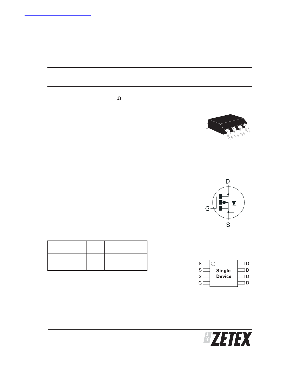
ORDERING INFORMATION
SO8
DEVICE REEL
SIZE
ZXMN3A02N8TA 7” 12mm 500 units
ZXMN3A02N8TC 13” 12mm 2500 units
TAPE
WIDTH
QUANTITY
PER REEL
DEVICE MARKING
•
ZXMN
3A02
ISSUE 3 - AUGUST 2003
PINOUT
Top View
1
SEMICONDUCTORS
ZXMN3A02N8
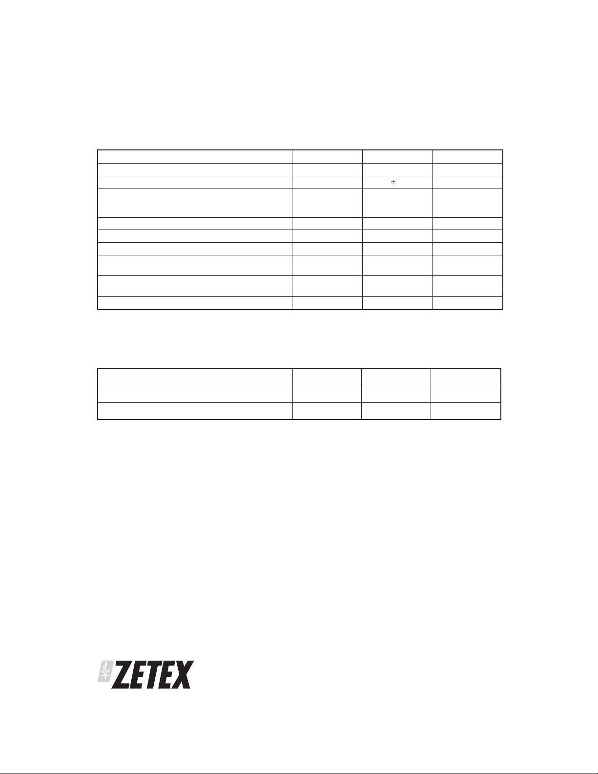
ABSOLUTE MAXIMUM RATINGS.
PARAMETER SYMBOL LIMIT UNIT
Drain-Source Voltage V
Gate Source Voltage V
Continuous Drain Current V
=-10V; TA=25°C (b)
GS
V
=-10V; TA=70°C (b)
GS
V
=-10V; TA=25°C (a)
GS
Pulsed Drain Current (c) I
Continuous Source Current (Body Diode) (b) I
Pulsed Source Current (Body Diode) (c) I
Power Dissipation at T
Linear Derating Factor
Power Dissipation at T
Linear Derating Factor
=25°C (a)
A
=25°C (b)
A
Operating and Storage Temperature Range T
DSS
GS
I
D
DM
S
SM
P
D
P
D
j:Tstg
THERMAL RESISTANCE
PARAMETER SYMBOL VALUE UNIT
Junction to Ambient (a) R
Junction to Ambient (b) R
NOTES
(a) For a device surface mounted on 25mm x 25mm FR4 PCB with high coverage of single sided 1oz copper, in still air conditions
(b) For a device surface mounted on FR4 PCB measured at t⭐10 secs.
(c) Repetitive rating 25mm x 25mm FR4 PCB, D = 0.02, pulse width 300s - pulse width limited by maximum junction temperature.
θJA
θJA
30 V
20 V
9.0
7.2
7.3
44 A
3.2 A
44 A
1.56
12.5
mW/°C
2.5
20
mW/°C
-55 to +150 °C
80 °C/W
50 °C/W
A
W
W
SEMICONDUCTORS
ISSUE 3 - AUGUST 2003
2
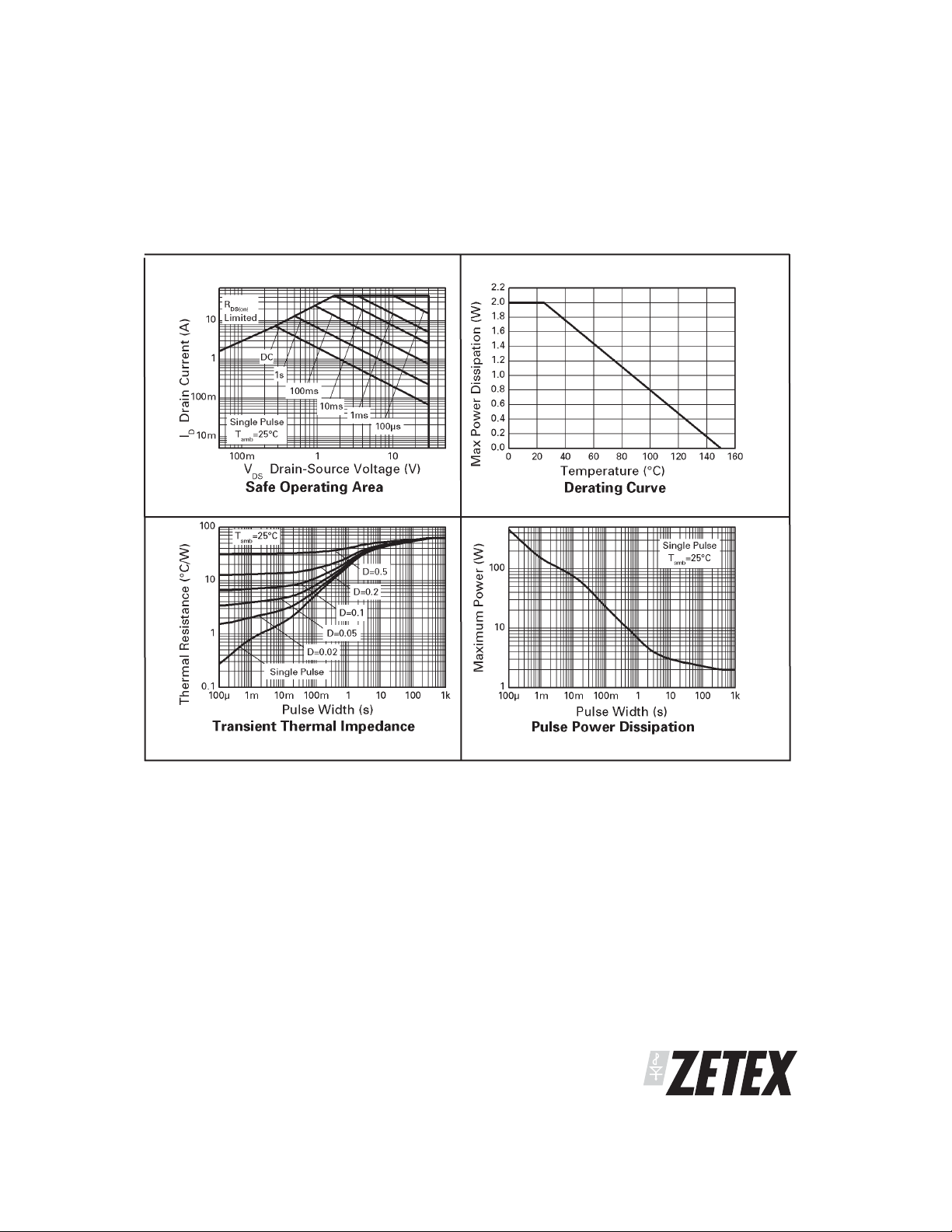
CHARACTERISTICS
ZXMN3A02N8
ISSUE 3 - AUGUST 2003
3
SEMICONDUCTORS
 Loading...