Zetex ZNBG2000, ZNBG2001 Datasheet

FET BIAS CONTROLLER
DEVICE DESCRIPTION
The ZNBG series of devices are designed to meet the
bias requirements of GaAs and HEMT FETs
commonly used in satellite receiver LNBs, PMR,
cellular telephones etc. with a minimum of external
components.
With the addition of two capacitors and a resistor the
devices provide drain voltage and current control for
2 external grounded source FETs, generating the
regulated negative rail required for FET gate biasing
whilst operating from a single supply. This negative
bias, at -3 volts, can also be used to supply other
external circuits.
The ZNBG2000/1 contains two bias stages. A single
resistor allows FET drain current to be set to the
desired level. The series also offers the choice of
drain voltage to be set for the FETs, the ZNBG2000
gives 2.2 volts drain whilst the ZNBG2001 gives 2
volts.
These devices are unconditionally stable over the full
working temperature with the FETs in place, subject
to the inclusion of the recommended gate and drain
capacitors. These ensure RF stability and minimal
injected noise.
ZNBG2000
ZNBG2001
It is possible to use less than the devices full
complement of FET bias controls, unused drain and
gate connections can be left open circuit without
affecting operation of the remaining bias circuits.
In order to protect the external FETs the circuits have
been designed to ensure that, under any conditions
including power up/down transients, the gate drive
from the bias circuits cannot exceed the range -3.5V
to 0.7V. Furthermore if the negative rail experiences a
fault condition, such as overload or short circuit, the
drain supply to the FETs will shut down avoiding
excessive current flow.
The ZNBG2000/1 are available in MSOP10 packages
for the minimum in devices size. Device operating
temperature is -40 to 80°C to suit a wide range of
environmental conditions.
FEATURES
•
Provides bias for GaAs and HEMT FETs
•
Drives up to two FETs
•
Dynamic FET protection
•
Drain current set by external resistor
•
Regulated negative rail generator requires only 2
external capacitors
•
Choice in drain voltage
•
Wide supply voltage range
•
MSOP surface mount package
ISSUE 1 - AUGUST 2001
APPLICATIONS
•
Satellite receiver LNBs
•
Private mobile radio (PMR)
•
Single in single out C Band LNB
•
Cellular telephones
1

ZNBG2000
ZNBG2001
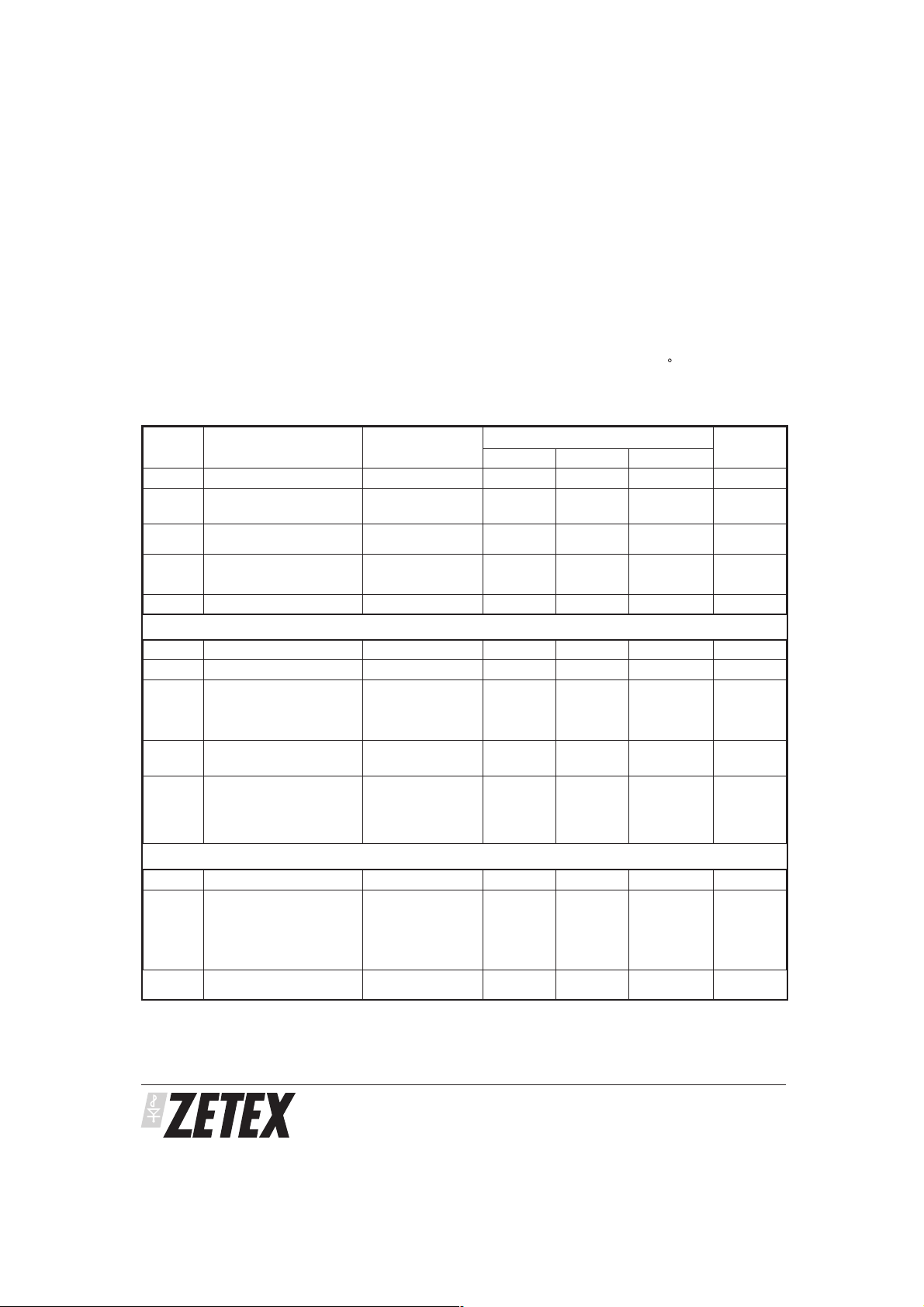
ABSOLUTE MAXIMUM RATINGS
Supply Voltage -0.6V to 15V
Supply Current 100mA
Drain Current (per FET) 0 to 15mA
(set by R
CAL1
and R
CAL2
)
ELECTRICAL CHARACTERISTICS TEST CONDITIONS (Unless otherwise
SYMBOL PARAMETER CONDITIONS
V
CC
I
CC
V
SUB
E
ND
E
NG
f
O
Supply Voltage 5 12 V
Supply Current ID1and I
Substrate Voltage
(Internally generated)
Output Noise
Drain Voltage
Gate Voltage
ID1and ID2=10mA
I
I
C
C
D2=0
=0
SUB
= -200µA
SUB
=4.7nF, CD=10nF
G
=4.7nF, CD=10nF
G
Oscillator Freq. 150 330 800 kHz
DRAIN CHARACTERISTICS
I
DO
I
D
⌬I
⌬I
V
⌬V
⌬V
DT
D
Output Current Range Set by R
CAL1
Current 8 10 12 mA
Current Change
DV
with V
with T
Voltage ZNBG2000
CC
j
VCC=5 to 12V 0.5 %/V
Tj=-40 to +80°C 0.05 %/°C
ID1and ID2=10mA 2
ZNBG2001
Voltage Change
with V
with T
CC
j
DV
DT
VCC= 5 to 12V 0.5 %/V
Tj= -40 to +80°C 50 ppm
GATE CHARACTERISTICS
I
GO
V
OL
V
OH
Notes:
1. The negativebias voltages specified are generatedon-chip using an internaloscillator. Two externalcapacitors, C
purpose.
2. The characteristics are measured using an external reference resistors R
3. Noise voltage is not measured in production.
4. Noise voltage measurement ismade with FETs and gateand drain capacitors in placeon all outputs. C
Output Current Range -40 2000
Output Voltage
Output Low ID1and ID2=12mA
Output High ID1and ID2= 8mA
and IG2=0 -3.5 -2 V
IG1
and ID2=12mA
I
D1
and IG2= -10µA
I
G1
and IG2= 0 0.4 1 V
I
G1
Output Current 100mA
Operating Temperature -40 to 80°C
Storage Temperature -40 to 85°C
Power Dissipation (T
amb 25 C)
MSOP10 500mW
LIMITS
UNITS
Min Typ Max
5
24
-3.5 -2.8 -2
10
30
-2
0.02
0.005
mA
mA
V
V
Vpkpk
Vpkpk
015mA
1.8
2.2
2
2.4
2.2
V
V
µA
-3.5 -2 V
and C
, of 47nFare required for this
SUB
to ground.
of value 16kΩ wired from pin R
CAL1
NB
CAL1
, 4.7nF, are connected betweengate outputs and
G
ISSUE 1 - AUGUST 2001
2

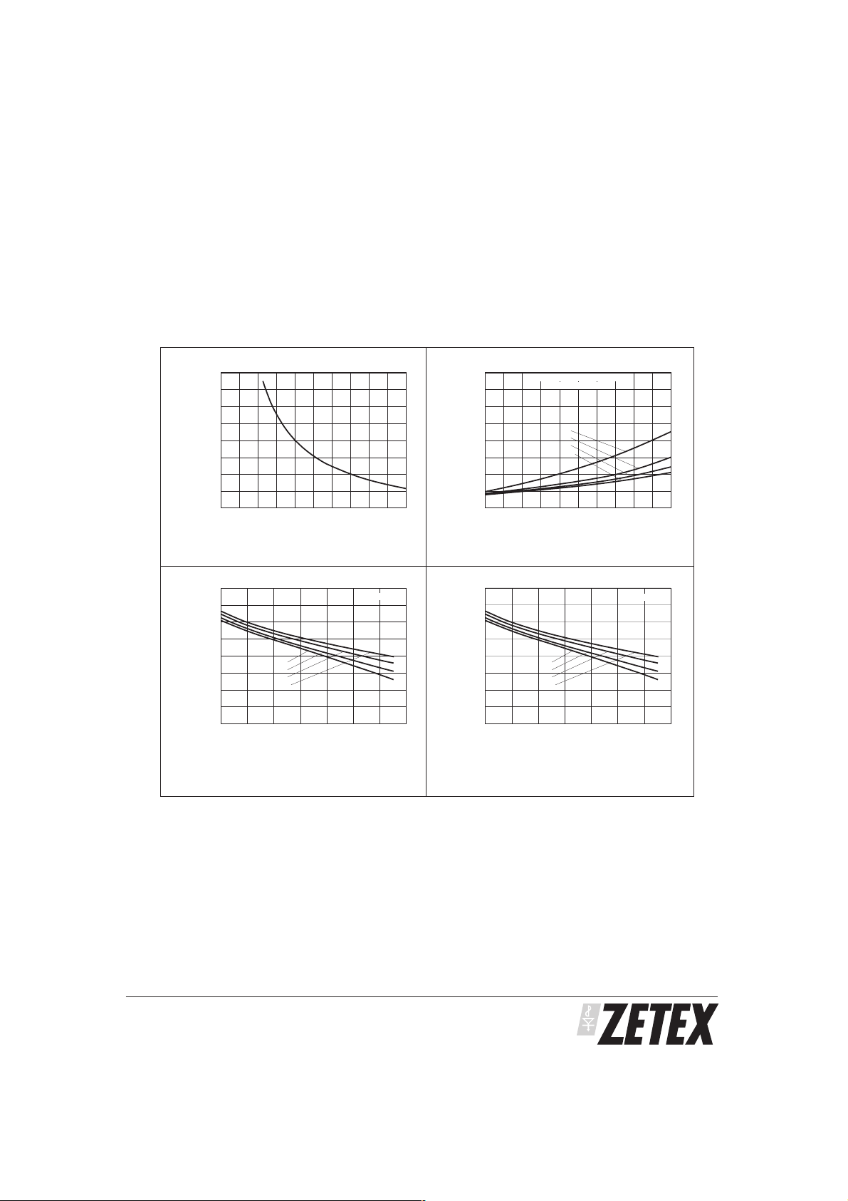
TYPICAL CHARACTERISTICS
ZNBG2000
ZNBG2001
16
14
12
10
8
6
4
Drain Current (mA)
2
0
0102030 50
Rcal (k)
JFET Drain Current v Rcal
2.4
2.3
2.2
2.1
Drain Voltage (V)
2.0
2468 16
Vcc = 5V
6V
8V
10V
10
12 14
Drain Current (mA)
JFET Drain Voltage v Drain Current
Vcc = 5V
40
ZNBG2000
Note:- Operation with loads > 200µA
0.0
-0.5
-1.0
-1.5
Vsub (V)
-2.0
-2.5
-3.0
0 0.2 0.4 0.6 1.0
is not guaranteed.
Vcc = 5V
6V
8V
10V
External Vsub Load (mA)
Vsub v External Load
2.2
2.1
Drain Voltage (V)
2.0
1.9
1.8
2
4
Vcc = 5V
6V
8V
10V
68
10 12 14 16
Drain Current (mA)
JFET Drain Voltage v Drain Current
0.8
ZNBG2001
ISSUE 1 - AUGUST 2001
5
3
 Loading...