

Page 1

SERVICE MANUAL
Model Series:
Product Type: Presentation Series
Chassis: CS
Manual Series: SR24
Manual Part #: 923-03509
Model Line: E
Product Year: 2002
CONTENTS
General Information/Remote Controls............... 1
Factory Menu ............................................... 2
Servicing/Troubleshooting ............................. 3
Model/Module Parts Lists ............................... 4
Exploded Views ............................................. 5
Schematics ................................................... 6
H27E46DT
H27E46DT8
H32E46DT
H36E46DT
Printed in U.S.A.
Published November 2002
by Technical Publications
Zenith Electronics Corporation
201 James Record Road
Huntsville, Alabama 35824-1513
Copyright 2002 by Zenith Electronics Corporation
Page 2
PRODUCT SAFETY SERVICING GUIDELINES FOR AUDIO-VIDEO PRODUCTS
A.C
d
IMPORTANT SAFETY NOTICE
This manual was prepared for use only by properly trained audio-visual service
technicians.
When servicing this product, under no circumstances should the original
design be modified or altered without permission from Zenith Electronics
Corporation. All components should be replaced only with types identical to
those in the original circuit and their physical location, wiring and lead dress
must conform to original layout upon completion of repairs.
Special components are also used to prevent x-radiation, shock and fire hazard.
These components are indicated by the letter “x” included in their component
designators and are required to maintain safe performance. No deviations are
allowed without prior approval by Zenith Electronics Corporation.
Circuit diagrams may occasionally differ from the actual circuit used. This way,
implementation of the latest safety and performance improvement changes into
the set is not delayed until the new service literature is printed.
CAUTION: Do not attempt to modify this product in any way. Never perform
customized installations without manufacturer’s approval. Unauthorized
modifications will not only void the warranty, but may lead to property damage
or user injury.
Service work should be performed only after you are thoroughly familiar with
these safety checks and servicing guidelines.
GRAPHIC SYMBOLS
The exclamation point within an equilateral triangle is intended
to alert the service personnel to important safety information in
the service literature.
The lightning flash with arrowhead symbol within an equilateral
triangle is intended to alert the service personnel to the presence
of noninsulated “dangerous voltage” that may be of sufficient
magnitude to constitute a risk of electric shock.
The pictorial representation of a fuse and its rating within an
equilateral triangle is intended to convey to the service personnel
the following fuse replacement caution notice:
CAUTION: FOR CONTINUED PROTECTION AGAINST RISK OF FIRE,
REPLACE ALL FUSES WITH THE SAME TYPE AND RATING AS MARKED
NEAR EACH FUSE.
SERVICE INFORMATION
While servicing, use an isolation transformer for protection from AC line shock.
After the original service problem has been corrected, make a check of the
following:
FIRE AND SHOCK HAZARD
1. Be sure that all components are positioned to avoid a possibility of
adjacent component shorts. This is especially important on items transported to and from the repair shop.
2. Verify that all protective devices such as insulators, barriers, covers,
shields, strain reliefs, power supply cords, and other hardware have been
reinstalled per the original design. Be sure that the safety purpose of the
polarized line plug has not been defeated.
3. Soldering must be inspected to discover possible cold solder joints, solder
splashes, or sharp solder points. Be certain to remove all loose foreign
particles.
4. Check for physical evidence of damage or deterioration to parts and components, for frayed leads or damaged insulation (including the AC cord), and
replace if necessary.
5. No lead or component should touch a receiving tube or a resistor rated at
1 watt or more. Lead tension around protruding metal surfaces must be
avoided.
6. After re-assembly of the set, always perform an AC leakage test on all exposed
metallic parts of the cabinet (the channel selector knobs, antenna terminals,
handle and screws) to be sure that set is safe to operate without danger of
electrical shock. DO NOT USE A LINE ISOLATION TRANSFORMER DURING THIS
TEST. Use an AC voltmeter having 5000 ohms per volt or more sensitivity in
the following manner: Connect a 1500 ohm, 10 watt resistor, paralleled by
a .15 mfd 150V AC type capacitor between a known good earth ground
water pipe, conduit, etc.) and the exposed metallic parts, one at a time.
Measure the AC voltage across the combination of 1500 ohm resistor and
.15 mfd capacitor. Reverse the AC plug by using a non-polarized adaptor
and repeat AC voltage measurements for each exposed metallic part. Voltage
measured must not exceed 0.75 volts RMS. This corresponds to 0.5 milliamp
AC. Any value exceeding this limit constitutes a potential shock hazard and
must be corrected immediately.
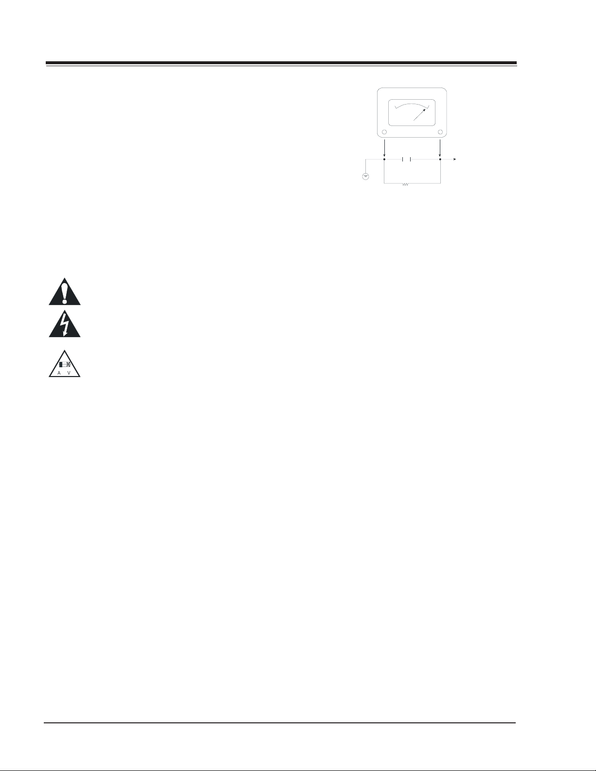
Good Eart h Ground
such as the Water
Pipe, Conduit, etc.
X-RADIATION
1. Be sure procedures and instructions to all service personnel cover the
subject of x-radiation. The only potential source of x-rays in current TV
receivers is the picture tube. However, this tube does not emit x-rays when
the HV is at the factory-specified level. The proper value is given in the
applicable schematic. Operation at higher voltages may cause a failure of
the picture tube or high-voltage supply and, under certain circumstances
may produce radiation in excess of desirable levels.
2. Only factory-specified CRT anode connectors must be used.
3. It is essential that the service personnel have available an accurate and
reliable high-voltage meter.
4. When the high-voltage circuitry is operating properly, there is no possibility
of an x-radiation problem. Every time a color chassis is serviced, the
brightness should be run up and down while monitoring the high voltage
with a meter, to be certain that the high voltage does not exceed the
specified value and that it is regulating correctly.
5. When troubleshooting and making test measurements in a product with a
problem of excessively high voltage, avoid being unnecessarily close to
the picture tube and the high voltage power supply. Do not operate the
product longer than necessary to locate the cause of excessive voltage.
6. Refer to HV, B+, and shutdown adjustment procedures described in the
appropriate schematics and diagrams (where used).
IMPLOSION
1. All direct view picture tubes are equipped with an integral implosion
protection system; take care to avoid damage during installation.
2. Use only the recommended factory replacement tubes.
TIPS ON PROPER INSTALLATION
1. Never install any receiver in a closed-in recess, cubbyhole, or closely
fitting shelf space over, or close to, a heat duct, or in the path of heated
air flow.
2. Avoid conditions of high humidity such as: outdoor patio installations
where dew is a factor, near steam radiators where steam leakage is a factor,
etc.
3. Avoid placement where draperies may obstruct venting. The customer
should also avoid the use of decorative scarves or other coverings that
might obstruct ventilation.
4. Wall- and shelf-mounted installations using a commercial mounting kit
must follow the factory-approved mounting instructions. A product mounted
to a shelf or platform must retain its original feet (or the equivalent
thickness in spacers) to provide adequate air flow across the bottom. Bolts
or screws used for fasteners must not touch any parts or wiring. Perform
leakage tests on customized installations.
5. Caution customers against mounting a product on a sloping shelf or in a
tilted position, unless the receiver is properly secured.
6. A product on a roll-about cart should be stable in its mounting to the cart.
Caution the customer on the hazards of trying to roll a cart with small
casters across thresholds or deep pile carpets.
7. Caution customers against using a cart or stand that has not been listed
by Underwriters Laboratories, Inc. for use with its specific model of
television receiver or generically approved for use with TVs of the same or
larger screen size.
8. Caution customers against using extension cords. Explain that a forest of
extensions, sprouting from a single outlet, can lead to disastrous
consequences to home and family.
. Voltmeter
0.15uF
1500 OHM
10 WATT
Place this probe
on each expose
metal part .
SR24 - 923-03509 CS - SAFETY
i
Page 3
PRODUCT SAFETY SERVICING GUIDELINES FOR AUDIO-VIDEO PRODUCTS
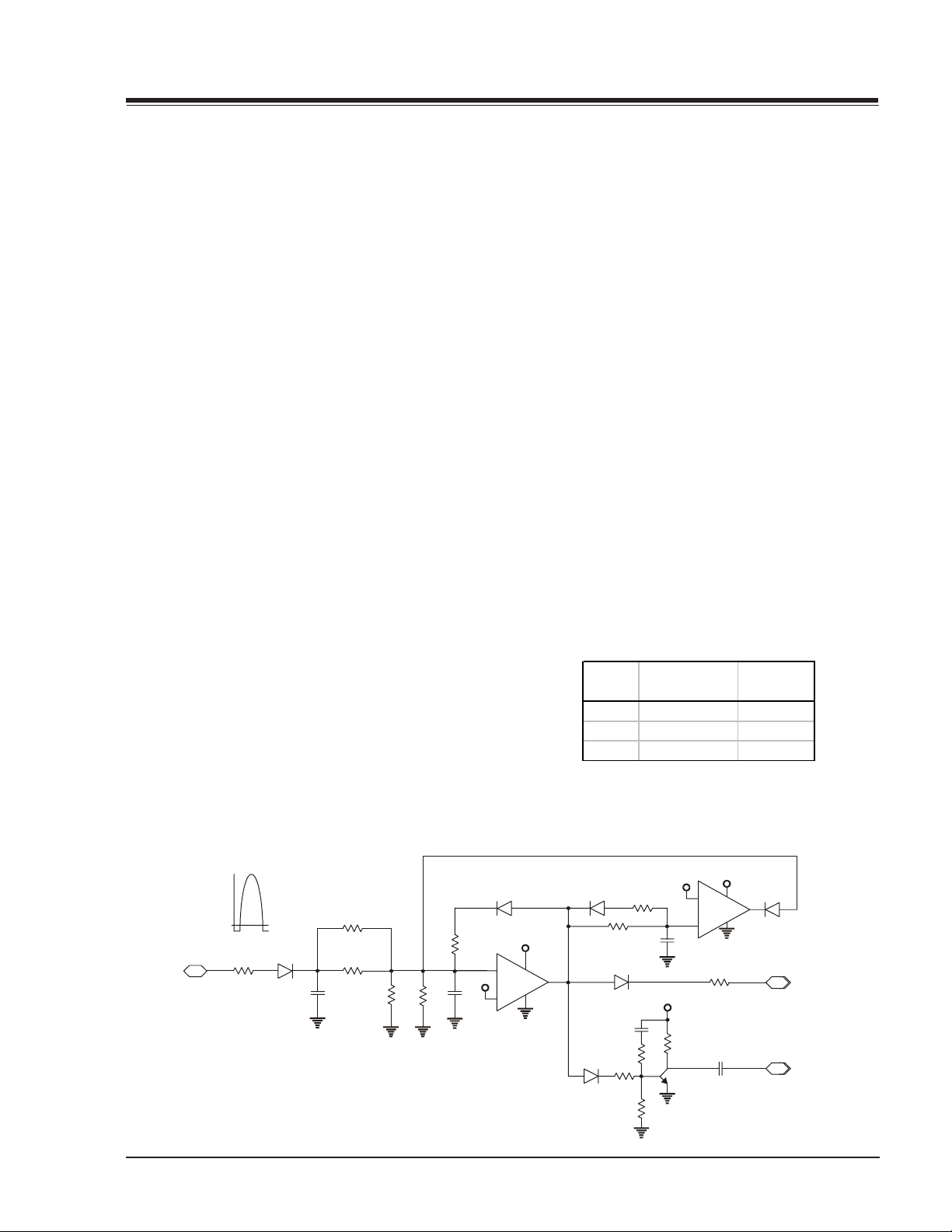
N
X-RADIATION
To prevent possible exposure to radiation caused by excessive
CRT Anode voltage, the CS Chassis incorporates a “High Voltage Shutdown” circuit. This circuit senses the level of flyback
pulse from the “Flyback Transformer” representative of the
actual high voltage on the CRT anode. When this level exceeds a predetermined voltage, the circuit shuts down the
horizontal drive, preventing further generation of anode voltage. In this condition, the horizontal drive is “latched” off for
about 5 seconds, after which, restart is attempted.
SHUTDOWN CIRCUIT OPERATION
The flyback pulse voltage from Pin 6 of TX3201 (Flyback Transformer) is peak detected (rectified) by the action of diode
D3206 and capacitor C3214. This forms a DC voltage appearing on C3214 representative of the CRT anode voltage (HV)
produced by T3201. This voltage is divided down by precision
resistors RX3214, RX3215, RX3216 & RX3217. This lower voltage, appear on the non-inverted input (pin 5) of IC3201.
If the CRT anode voltage become excessive, pin 5 of IC3201
will be higher than inverted input of pin 6. This will cause the
output of pin 7 to rise to approximately 15 volts. This signal
(SD_DRV) is sent to the base of Q4000 causing Horizontal
Drive to be disabled and latched, which causes the HV to
shutdown. In about 5 seconds, the shutdown circuit resets
(Pins 8, 9 & 14 of IC2900), the Horizontal Drive and HV will be
reestablished. The circuit formed by Q2907, C2913, C2916,
D2908, R2923, R2935, R2936, and R2937 disables the HV
compensation output (Q2902-b signal) during turn on and shutdown conditions (transients).
CRT ANODE HIGH VOLTAGE MEASUREMENT PROCEDURE
Each CRT screen has it’s own safe operating Anode Voltage
and shutdown voltage. Critical Safety components (designated
with an ‘X’ in the component designator) are designed to
operate the CRT at a safe operating Anode voltage and provide proper shutdown thresholds. If replacement of any of
these components is deemed necessary, it is important to use
original type Zenith replacement components.
After a replacement is made, confirm proper Anode voltage
using the following procedure.
Measurement of the CRT Anode voltage must be performed
with no visible raster on the screen and operating at nominal
horizontal scanning frequency 15.734 or 37.9 Khz (TV or SVGA
signal).
After discharging the CRT, connect a high impedance high
voltage meter to the CRT anode. Turn the television ‘On’ and
confirm good signal is being displayed. Reduce Brightness
and Contrast settings until the picture is well extinguished.
Observe the Anode voltage meter reading and compare with
the table below for the proper CRT screen size. If the voltage
reading is higher than the maximum, verify circuit component
values and proper operation.
HV SHUTDOWN MEASUREMENT PROCEDURE
1. Adjust the beam current to 0 mA in NTSC mode.
2. Apply a variable DC voltage to pin 10 of the PTD1 connector, from 20 to 0 Vdc, starting at 20 Vdc.
3. Slowly decrease supply towards zero.
4. Remove DC voltage from pin 10 of PTD1.
5. After approximately 5 seconds, verify that the HV is reestablished (High Voltage Reset).
IN
From Pin 6, T3201
RX3213
Flyback Pulse
D3206
C3214
RX3215
RX3214
SHUTDOWN SAFETY CIRCUIT
D3207
R3221
+
+5V
RX3216
RX3217
C3215
-
+15V
V+
V-
IC3201
Screen
Size
HV Nominal
Level (k V)
27" 27 29
32" 30 31.5
36" 30 31.5
+15V
+5V
D2909
D2908
R2943
D4002
C2916
R2935
R2936
R2937
R2944
C2917
+15V
R2923
Q2907
9
+
V+
IC2900
V-
8
-
R4015
C2913
HV Max
Level (k V)
D2910
14
To Base of Q4000
OUT
SHUTDOWN
(SD_DRV)
To Base of Q2902
OUT
HV COMPENSATIO
DISABLE
SR24 - 923-03509 ii CS - SAFETY
Page 4

- iii -
Page 5

TABLE OF CONTENTS
SECTION 1 OVERVIEW
OVERVIEW ............................................................. 1-1
CONNECTIONS ........................................................ 1-2
CONNECTIONS ................................................. 1-2
REMOTES ............................................................... 1-6
PROGRAMMING THE REMOTE .............................. 1-7
AUTO FIND ..................................................... 1-7
CABLE BOX ..................................................... 1-7
VOLUME OVERRIDE ........................................... 1-7
AUXILIARY CAPABILITY ..................................... 1-7
QUICKSET II PROGRAMMER ................................ 1-9
USER MENUS ....................................................... 1-12
SETUP MENU ................................................. 1-12
AUDIO MENU ................................................ 1-14
VIDEO MENU ................................................. 1-14
PARENTAL CONTROL ........................................ 1-15
SOURCE MENU............................................... 1-17
SOURCE MENU............................................... 1-17
ALTERNATE SOURCE MENU BY TV/SOURCE KEY ... 1-17
VIDEO SOURCE INPUT ..................................... 1-19
COMPUTER SOURCE INPUT ............................... 1-20
SECTION 2 SERVICE MENU
SERVICE MENU ....................................................... 2-1
FACTORY MENU ITEMS ...................................... 2-3
FACTORY MENU TABLES .................................... 2-8
SECTION 6 SCHEMATICS
AUDIO/VIDEO SWITCH ............................................. 6-1
VIDEO CHROMA PROCESSOR ..................................... 6-2
VIDEO PROCESSOR .................................................. 6-3
VIDEO SYNC PROCESSOR ......................................... 6-4
AUDIO PROCESSOR ................................................. 6-5
IF DEMODULATOR ................................................... 6-6
MICROCONTROLLER ................................................. 6-7
MPI CARD .............................................................. 6-8
EDGE CARD ............................................................ 6-9
POWER SUPPLY ..................................................... 6-10
HORIZONTAL & VERTICAL DEFLECTION ...................... 6-11
POWER SUPPLY DAUGHTER BOARD .......................... 6-12
DYNAMIC FOCUS DAUGHTER BOARD ........................ 6-13
VIDEO OUTPUT ..................................................... 6-14
SECTION 3 SERVICING
CIRCUIT OVERVIEW ................................................. 3-1
CHASSIS OVERVIEW ......................................... 3-1
VIDEO PROCESSING................................................. 3-2
AUDIO PROCESSING ................................................ 3-5
POWER SUPPLY ....................................................... 3-6
DEFLECTION AND HIGH VOLTAGE ............................... 3-8
PURITY & CONVERGENCE SETUP PROCEDURE ............. 3-12
ADJUSTMENTS ...................................................... 3-13
IC DESCRIPTIONS ................................................. 3-14
SECTION 4 PARTS
MODEL PARTS ........................................................ 4-1
SECTION 5 DIAGRAMS
27” EXPLODED VIEW ............................................... 5-1
32” EXPLODED VIEW ............................................... 5-2
36” EXPLODED VIEW ............................................... 5-3
INTERCONNECT DIAGRAM ......................................... 5-4
LARGE SIGNAL PCB ................................................. 5-5
SMALL SIGNAL PCB TOP ........................................... 5-6
SMALL SIGNAL PCB BOTTOM ..................................... 5-7
SR24 - 923-03509 TOC CS - TOC
Page 6

Page 7
SECTION 1
OVERVIEW
IC5141
VIDEO OUTPUT
G2
IC5121
5F4
2K6
2G9
10VGA1
2B4
2C5
2C4
6F1
2P6
8VGA2
IC1400
ICX2900
JACKPACK
1
4A8
4B8
2G4
2A3
2H4
2V4
2S2
IC801
1
CRT1
DAG2
4T8
FOCUS
DAG1
IC5161
ICX3400
1
LX3400 4R8
1
5C2
1
TX3401
TERMINAL 3RD WIRE
GROUND FOR HOSPITAL
AND EDUCATIONAL
MARKETS
EX3400
Q2904
PTD2
DX3200
RED
PTD1
4H2
4G2
4D3
BLUE
4
X
4
4Y4
4V2
1
ICX2100
4B2
4A3
D3404
4C2
4F5
AA
Q3202
Q4103
QX3200
T
3
D4102
T4000
2
0
1
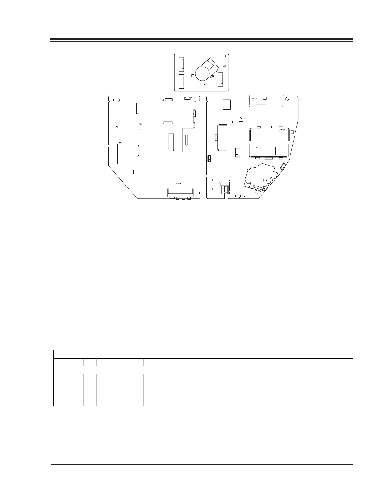
The CS series chassis will be used on the E-Line Commercial Products. The Presentation Series PC-to-TV monitor
receivers were designed for educational and business
applications. This manual covers 27, 32, and 36 inch
screen sizes. The concept of this chassis is to make one
main board for all models and one power supply board
for all models in a particular screen size. Additional plug
in boards with jack packs may be added to the chassis
to accommodate the different features.
The CS series chassis features 11 IC’s and 3 peripheral
devices for all signal, sync and sweep processing. The
ICX2200 handles the Base Band signal processing, the
RGB processing, and video switching for 4 systems (HV
sync signal processing included).
ICX2201 integrates the luminance signal processing,
Chroma signal processing, and the sync signal. The
ICX2600 was developed for various types of direction
compensation for point scan/multi scan TVs. The IC1400
includes functions such as stereo modulation, SAP (Separate Audio Program), dBx noise reduction, and sound
processing. The IC2900 is an A/V switch which determines which auxiliary video and audio signals will be
processed by the video processor, also it can switch the
IF video signal. IC6000 is the main microprocessor and
IC6001 is the main memory.
All CS models are module level repair only. The table below contains basic information on the Presentation Series. For more datails please see the Interconnect Diagram in this Manual (section 5).
CS Ch assis Mo del Information
MODEL SCR CABINET JACKS EXTRA FEATURES RESOLUTION REMOTE MICRO OP GUIDE
ALL MODELS ARE MODU LE LEVEL REPAIR
H27E46DT 27 Table Top 11 VGA card and MPI card 800x600 124-00233-04
H27E46DT8 27 Table Top 11 VGA card and MPI card 800x600 124-00233-04
H32E46DT 32 Table Top 11 VGA card and MPI card 800x600 124-00233-04
H36E46DT 36 Table Top 11 VGA card and MPI card 800x600 124-00233-04
P221-1391-P07
P221-1391-P07
P221-1391-P07
P221-1391-P07
206-03755
206-03755
206-03755
206-03755
SR23 - 923-03509 1-1 CS - GENERAL
Page 8
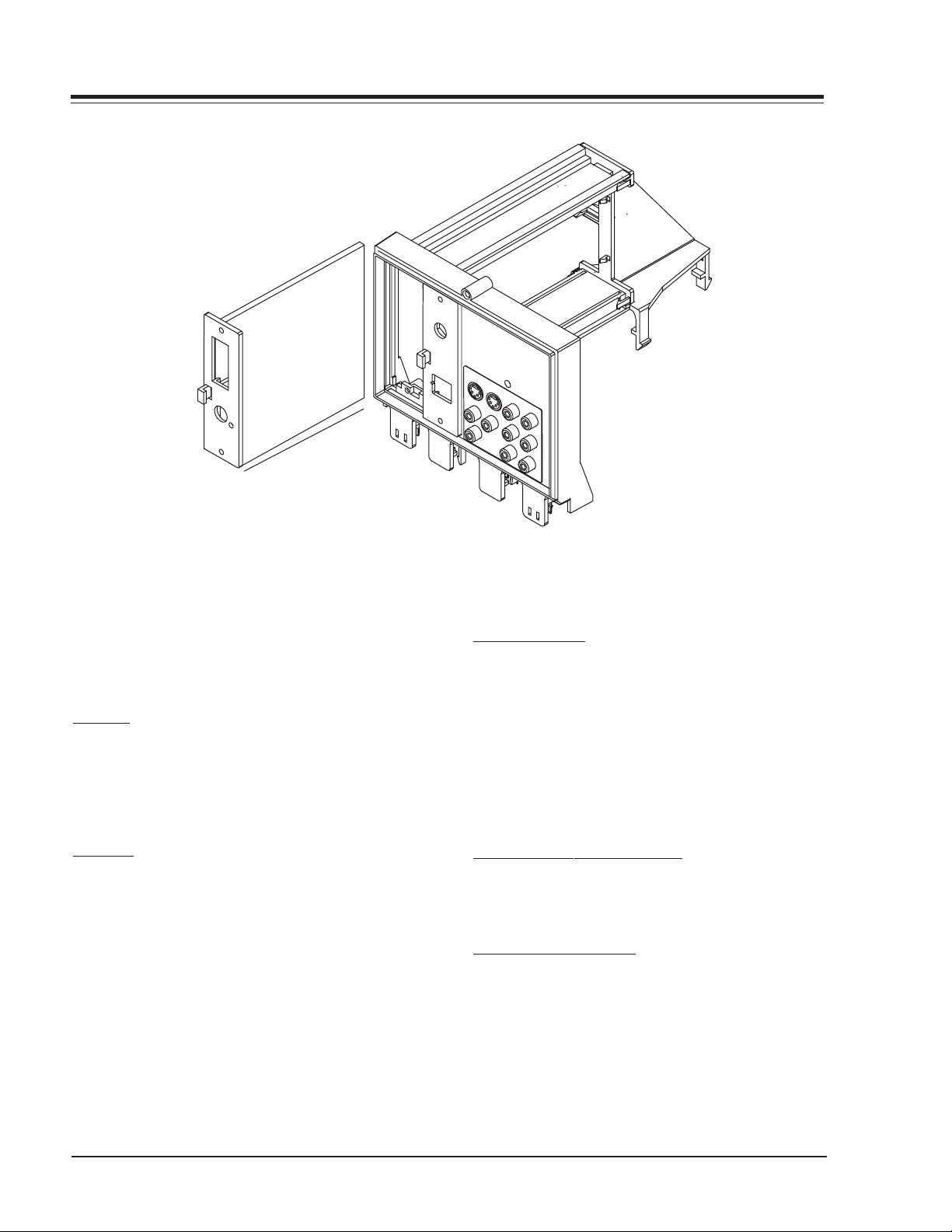
CONNECTIONS
CONNECTIONS
The connection center on the rear of the TV allows for
connection of the viewing source. The diagrams on the
next page list the use of each jack on the connection
center.
OUTPUTS
S-Video Loop out luminance is on pin 34 and chroma is
on pin 32 of ICX2900. The analog stereo comes from
pins 6 and 7 of IC1400 before running through a preamplifier circuit. After the pre-amp stage, the audio passes
to the jackpack.
CAMPORT
Some models have video and right/left audio input jacks
on the front of the receiver. These jacks can be used to
view video tapes from a VCR or Camcorder. When the
video cable is plugged into the jack, the shorting jack
J1 opens, placing a high at pin 10 of the IC6000 microprocessor. This switches the TV into the auxiliary mode.
As long as the cables are attached, the TV set will be
locked in auxiliary mode. Use of a remote control or
buttons on the front of the set will not permit switching into tuner mode until the video cable is discon-
nected.
SUPERPORT - MPI
Zenith Commercial Product receivers are now being
adapted to interact with other equipment. Prime examples of this can be found in Lodging and Health Care
situations where the set is controlled from the main office.
All this is made possible by the new technology that is
being built into these receivers. The SuperPort or Multiple Protocol Interface (MPI) jack and associated circuitry allow remote operation of the set.
MULTIPLE PROTOCOL INTERFACE
Television functions and features are controlled by the
communication of commands and status information
through the Superport by the MPI interface.
EBC (EDGE BOARD CARD)
Allows easy access for removing/installing accessory
modules providing a rail mounted slide-through card.
SR23 - 923-03509 1-2 CS - GENERAL
Page 9
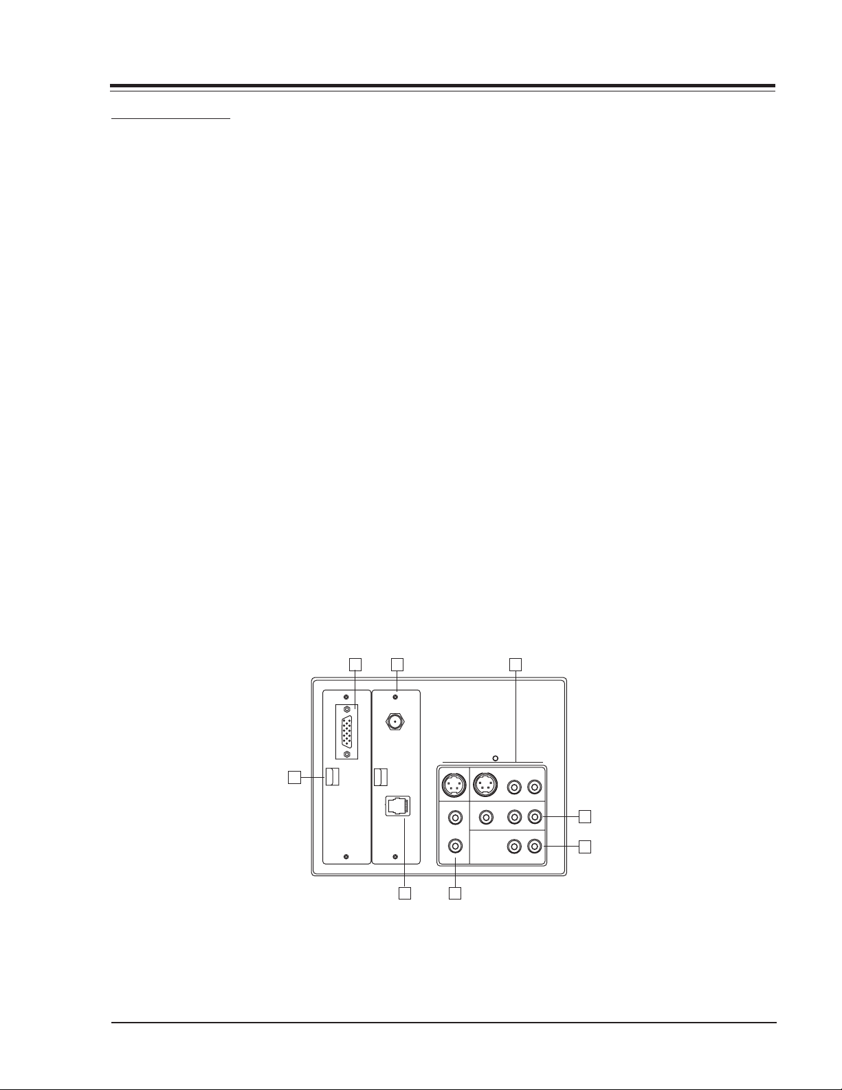
CONNECTIONS
CONNECTION CENTER
1. COMPUTER VIDEO INPUT (HD15)
Standard DB15 receptacle for SVGA input video signal
from either PC or Macintosh format. This provides a
“Flicker-Free” view of the computer.
2. ANTENNA/CABLE JACK
This jack is used for 75-ohm antenna-type signal connections to the TV. Attach antenna, cable TV line, or
other video equipment to jack. The input cable may come
from an outdoor or master antenna, cable TV line, cable
decoder box, or the RF output from a VCR.
3. S-VIDEO IN AND OUT
These jacks are for input and output connections to
SUPER-VHS video equipment. Use the input jack for viewing S-Video. Use the output jack to loop the S-Video
signal to an additional TV or monitor. The right and left
audio jacks are used for the stereo input or output paired
with the S-Video Signal.
4. VIDEO IN AND AUDIO IN
Use the Video and Audio In jacks for baseband video
and audio input signals from a VCR or other signal source.
To view the signal input to these jacks, select the AUX
channel on the TV.
5. COMPUTER AUDIO IN
These jacks provide left and right audio input that can
be paired with the computer data input.
6. AUDIO OUT
These jacks provide preamp audio out to be used with
an external amplifier.
7. MPI (MULTIPLE PROTOCOL INTERFACE) JACK
Standard RJ11 jack to provide interface with in-room
entertainment and video services. Also used with the
installer’s remote control for programming other TVs in
the system with the same features as the master TV.
8. POWER INDICATOR
The Scan Card power indicator LED (if the set has a Scan
Card).
9. SUPERPORT
Allows easy installation of an accessory module without
removing the cabinet back. Module is housed inside the
TV cabinet and receives operating power and all necessary interface signals through internal connections.
S-VIDEO IN
VIDEO
COMPUTER
AUDIO
AUX IN
3
--AUDIO--
RL
--AUDIO--
RL
--AUDIO--
RL
4
5
1
9
2
ANTENNA
C
CABLE
O
M
P
U
T
E
R
I
N
M. P.I.
S-VIDEO OUT
R
AUDIO OUT
L
7
6
SR23 - 923-03509 1-3 CS - GENERAL
Page 10
p
p
CONNECTIONS
CONNECTING TO A COMPUTER
Installed in the certain units is the PCZTV internal scan
converter, provided by FOCUS Enhancements, Inc. This
allows the receiver/monitor to be used as a large screen
device to view VGA video output of a PC or Macintosh
format computer. In order to view these computer images, connect the computer to the Super Port input,
turn on the receiver/monitor, set it to the appropriate
source and activate your computer.
ANTENNA
C
CABLE
VIDEO OUT
O
M
P
U
T
E
R
I
N
M. P. I.
S-VIDEO IN
S-VIDEO OUT
R
AUDIO OUT
L
Connect to the audio output
on the com
VIDEO
COMPUTER
--AUDIO--
RL
AUX IN
--AUDIO--
RL
--AUDIO--
RL
AUDIO
uter.
Connect to the
video output on
the computer
(DB 15).
In addition, the computer images may also be recorded
onto video tape if a VCR is connected in as shown in the
illustration.
ANTENNA
CABLE
C
O
M
P
U
T
E
R
I
Connect to the video
input on the VCR.
VIDEO OUT
N
M. P. I.
Connect to the audio
in
S-VIDEO IN
S-VIDEO OUT
VIDEO
R
AUDIO OUT
L
COMPUTER
ut on the VCR.
--AUDIO--
RL
AUX IN
RL--AUDIO--
--AUDIO--
RL
AUDIO
FORMATS
Compatible Video Formats
Resolution Refresh
640 x 480 60 Hz
640 x 480 72 Hz
800 x 600 60 Hz
800 x 600 67 Hz
1024 x 767 60 Hz
DOS TEXT 70 Hz
640 x 480 67 Hz
832 x 768 67 Hz
CABLE AND ACCESSORIES KIT
Included with this new receiver/monitor is an accessories kit which provides the necessary items for connecting a computer to the Super Port jack. The kit includes
the following:
Accessories Kit
Quantity Accessory Item
1
1
1 HD DB15 Female to DB15 Male adapter.
1
CONNECTIONS
If the computer provides video out via a DB15 jack (15
pins aligned in two rows), the HD DB 15 to DB15 adapter
will have to be used. Plug the DB15 side of the adapter
into the DB15 video out of the computer. Then connect
the 15-foot video cable, between the HD DB15 side of
the adapter and the HD DB15 jack of the Super Port.
15 foot VGA interconnect cable. HD DB15
Male to HD DB15 Male.
10 inch Computer Video interconnect cable.
Male phone to Male phono (Cable C).
3½ floppy disk: Accessory Video driver
software.
(Instructions included separately)
SR23 - 923-03509 1-4 CS - GENERAL
Page 11
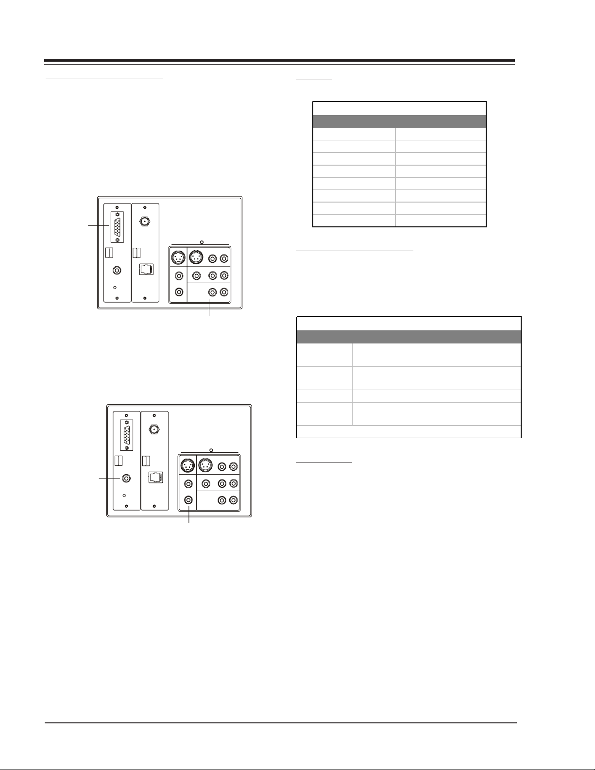
CONNECTIONS
d
p
HD DB15
(15 pins aligned
in thre e rows)
DB15
(15 pins aligne
in two rows)
HD DB15 Femal to DB15 Male Ada
ter
DB15 Pin Descriptions
Pin Connection Pin Connection
1 Red Video Input 9 No Connection
2 Green video Input 10 Digital/Sync (mode)
3 Blue Video Input 11 Reserved (mode)
4 Reserved 12 No Connection
5 Reserved (test) 13 Horizontal Sync
6 Red Video Ground 14 Vertical Sync
7 Green Video Ground 15 No Connection
8 Blue Video Ground
USING PCZTV
Once the connections to the receiver monitor have been
completed, the receiver/monitor can be used to view
images from the computer.
1. Turn on the receiver/monitor
2. Tune the receiver/monitor to the appropriate source.
3. Turn on the computer.
4. The computer images should be visible on the screen.
RECORDING THE COMPUTER IMAGE
If your VCR has an video input jack, the computer images can be recorded to video tape. Connect the VCR as
described by the illustration on the previous page.
This jack pack provides L/R audio input paired with computer data input which will allow recording of audio
along with the video images. Your computer must provide audio out that can be connected to the jack pack
input on the receiver/monitor.
CHOOSING A DESKTOP PATTERN
Because of a television’s low resolution (as compared to
that of a computer monitor), avoid using computer desktop patterns that consist of elaborate designs or colors.
These can tend to vibrate or distort on the screen.
The recommended desktop pattern is either Black, a limited gray design, or some other solid dark color.
VIDEO DISTRIBUTION AMPLIFIER
If your receiver/monitor will be part of a closed circuit
network using a cable that is longer then 25 feet, or if
several sets will be used together using the loop out
jack, then a video distribution amplifier will probably
be necessary to ensure adequate signal strength is provided. These types of amplifiers can be purchased separately in many consumer audio/video stores.
VIDEO ADJUSTMENT
Adjustments to the computer video image are controlled
through the remote control. The 2 and 8 buttons shift
the display vertically. The 4 and 6 buttons shift the display horizontally. 1 is Zoom, 0 is freeze, and 5 gives
menu access.
SR23 - 923-03509 1-5 CS - GENERAL
Page 12
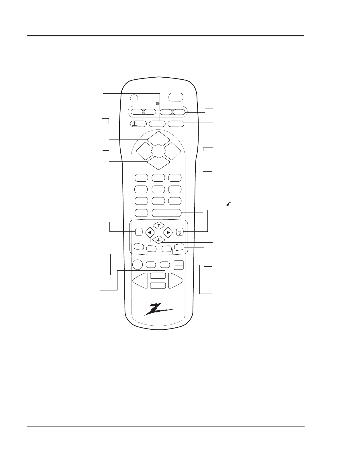
REMOTES
FLASHBK (Flashback)
Returns to previous Channel.
SURF
Turns Surf Channel On/Off
CHANNEL (Up/Down)
Selects next channel in
TV’s memory. Press
and hold to repeat.
NUMBER PAD
Selects channels directly.
REMOTE INFO
PRG
CABLE
SURF
VCR
FLASHBK
CHANNEL
VOLUME
CHANNEL
1
4
POWER
AUX
MUTE
VOLUME
3
2
5
6
POWER
Turns TV On or Off.
TV
MODE
Selects the remote's mode of operation
MUTE
Turns sound Off and On
while picture remains.
VOLUME (Left/Right)
Increases TV’s sound level.
ENTER
Shows Channel/Time, enters
channel, or removes any
on-screen menus.
MENU
Displays menus for TV
and other options.
LEFT/RIGHT ARROWS
Chooses and shows the
desired menu option.
A, B, C Keys
Special features of some TV’s
TIMER
Displays the Sleep Timer menu.
Press repeatedly to set desired
TV shut-off time.
7
0
MENU
A
RECORD
REWIND
B
PAUSE
8
ENTER
C
TIMER
PLAY
STOP
MBR3447C
124-00233-04
9
TV/VCR
SOURCE
FFWD
QUIT
CC
QUIT/ (Three Functions Key)
Exits from on-screen display, turns
the sound enhancement feature on
or off, and switches audio between
Main source and PIP source.
UP and DOWN ARROWS
Moves highlighted bar within
menu to select an option.
CC
Displays closed caption menu.
TV/VCR SOURCE
Steps through source options.
SR23 - 923-03509 1-6 CS - REMOTES
Page 13

REMOTE INFO
PROGRAMMING THE REMOTE
If you’re using Zenith products, the remote is already
programmed for most common codes: TV = 101, VCR =
201, CABLE = 353, and AUX = 401. For other brands, or
if your remote fails to control your Zenith products, you’ll
have to program the remote.
After installing the batteries, follow these steps for each
product:
1. Press and hold PRG using a blunt pointed object.
Release PRG after the indicator light turns on.
2. Press the device button to be programmed (CATV,
VCR, AUX, or TV).
3. Enter the 3-digit product code from chart on next
page.
4. Press and release ENTER to save the code.
5. Point the remote at product and press POWER to test
the product’s operation. If it does not turn on,
reprogram remote using a different code.
6. Write the codes on the label inside the battery
compartment for future reference.
AUTO FIND
If none of the codes in the code table operate your
equipment, use Auto Find to search for the proper code.
1. Turn on the product you want to operate.
2. Press and hold PRG using a blunt pointed object.
Release PRG after the indicator light turns on.
3. Press the key to be programmed (CATV, VCR, AUX, or
TV).
4. Enter “000”, then press ENTER within two seconds.
Auto Find is active after the indicator light flashes
and remains lit.
5. Point the remote at the product.
6. Press and release POWER repeatedly, about once a
second, until your product turns off. The indicator
light turns off when you press POWER and on when
you release it.
7. Press ENTER immediately to save the code. The
indicator light flashes to indicate the code has been
saved.
8. Press POWER to turn On your product.
9. Test your product. If the remote fails to operate some
of the basic functions, use Auto Find again to search
for a better code. (Auto Find resumes its search after
the last code that was entered and saved in step 7).
NOTE: If the indicator light stays on as you press
POWER, Auto Find has tried all of the codes. If
the product you want to control has not turned
off, your remote will not work with that product.
To cancel Auto Find, press PRG at any time during
Auto Find.
CABLE BOX
This remote can control the cable/converter box volume
and muting (instead of the TV’s) if available on your
equipment.
1. Program the cable/converter box normally.
2. After programming the cable/converter box, Press and
hold PRG again using a blunt pointed object. Release
PRG after the indicator light turns on.
3. Press and release the device button the cable box is
assigned to.
4. This time, enter the special code 3-9-9 instead of
the product code.
5. Press and release ENTER to save.
VOLUME OVERRIDE
These remotes can override TV, VCR, or Video Disk Player
volume functions with an amplifier’s volume and muting.
1. Program the amplifier normally.
2. After programming the amplifier, Press and hold PRG
again using a blunt pointed object. Release PRG after
the indicator light turns on.
3. Press and release the device button whose volume
control is to be replaced by the amplifier volume
control. For example, pressing TV will operate the
amplifier’s volume while the remote is in TV mode.
4. This time, enter the special code 4-9-9 instead of
the product code.
5. Press and release ENTER to save.
AUXILIARY CAPABILITY
This remote can control up to seven devices. If the remote has been programmed for four components using
the TV, VCR, CABLE, and AUX keys, you may also program
it for up to three additional using AUX+1, AUX+2, and
AUX+3.
TO PROGRAM AUX+1, AUX+2, AND AUX+3
1. Locate three-digit code for product in code table.
2. Press and hold PRG until indicator lights up.
3. Press the AUX and 1 simultaneously to select AUX+1.
4. Enter the three-digit code and press ENTER. The indicator light should flash and then turn off to indicate
the code has been accepted. If the light stays on,
repeat steps 3 and 4 or try a different code.
5. Repeat steps 2-4 for AUX+2 and AUX+3.
6. Write the codes on the label inside battery compartment for future reference. Hold down AUX and press
1, 2, or 3 to access AUX+1, +2, or +3 mode.
SR23 - 923-03509 1-7 CS - REMOTES
Page 14
REMOTE INFO
o
TV's
Daewoo 149 ProScan 216,260,266, Sprucer 313 Sharp 441,442
Zenith 101,121,149 282,725 Stargate 326,379 Sherwood 449
152 Quasar 259 ,29 5 St andard Co mp 33 5 Hit achi 950
TV/VCR
Adventura TV/VCR 154 240,242,249, Tocom 317,318,34 6 Luxman 930
Daewoo TV/VCR 148 260,266,282, Unika 325,348,362 M agnavox 421,422,433,
Funai TV /V CR 154 283,284,285, Universal 325,358,362 434
Goldstar TV/VCR 153,172 286,287,288, V id Tech 340 Sony 420,443,444,
Symphonic TV/VCR 154 708,710,711, Video Way 349 445,934
Zeni th TV / VC R 150, 153 ,154 72 5 V iew star 3 27,3 54,3 55, So undesig n 4 61,49 8,9 01,
172 R eali sti c 212,2 13 ,26 5, 372 90 2
VCR's
Admiral 261 Salora 297 Technics 432
Akai 292,717,718, Samsung 220,230
719,720 Sansui 289,292,709, Alphastar 516 Zenith CD Rec
Audio Dynamics 726 726 Chaparral 501,502 Zenith 460,461,498,
B ell + Ho well 2 47 Sanyo 2 12 ,24 7,29 4 Cheyenne 50 2 9 01,90 2
Broksonic 221,250,255, Scott 243,290,729 Dishnet 515
72 9 Sears 2 11,212, 213, D rake 50 3
Cand le 727 2 65,2 74 GE 510 ,517 Ci ti zen 9 14
Cano n 70 4 Sharp 2 61,730 Gener al Ins tr uments 504 ,505 GE 9 16
Cap eheart 72 8 Sig nat ure 2 00 0 216,2 19 ,2 49 Hi tachi 519 ,520 Go ld st ar 460,474
Citizen 727 Sony 232,723,724 Hughes Network 514 Hit achi 919
Cr aig 2 12 Syl vania 275,2 9 7 JV C 518 JV C 90 8
Curtis Mathes 259,266,725, Tatung 268,292 Macom 314 Kenwood 484
72 7 Teac 2 68 M ag navo x 52 1 Luxman 4 67
Daewoo 244,246,248, Teknika 272 Philips 521 M arantz 903,913
254,703,729 Toshiba 213,274,290, PrimeStar 513 Memorex 485
Daytron 246 297 ProScan 510,517 Nad 904
DBX 726 Vecto r Research 726,72 7 RCA DSS 373 Nakami chi 49 3
Electrohome 730 Victor 726 RCA 510,517 Onkyo 471,906
Emerson 203,221,243, Video Concepts 726,727 Realistic 506 Optimus 905
250,293,721, XR - 1000 243 Sierra I 502 Panaso nic 9 12
72 2,72 9,73 0, Y amaha 726 Sier ra II 50 2 Pi oneer 470 ,485,9 07
731,732 Zenith 201,224,225, Sierra III 502 Proton 910
Fisher 211,212,213, 229 Sony 511 Quasar 912
247,265,274 STS1 507 RCA 909
GE 216,220,266, STS3 508 Sharp 483,917,918
282,701,70 2,
725 Allegro 358,362 Uniden 522 Sony 486,489,490,
Go Video 256,262,263, A llegro A-B Switch 361 United 344 491,492
700 Archer 325 Zenith Drake 312,328,330 Soundesign 461,498,901,
Go ld st ar 2 53 Cent ury 32 5 Zeni th 351,378 ,50 0 9 02
Harman Kardon 296 Citizen 325 Toshiba 915
Hitachi 257,270,273, Comtronic 326
292,705,706, Everquest 379 Sony 452 Victor 908
707,708 Garrard 325 Zenith 460,461,498,
JC Penney 268,726 GE 367
Jensen 292 Gemini 305,331,338 ADC 940
JVC 224,225,258, General Inst rument 304,305,306, ADO 939
268,292,299, 307,308,309 , Aiwa 938 JVC 965
72 6 3 10 ,318 A kai 9 37 M it subi shi 96 4
Kenwood 268,292,726, Hamlin 302,303,345, Denon 935 Pioneer 9 63
72 7 3 65,3 66 Dy natec h 953 So ny 96 2
Magnavox 275 Jasco 325 Emerson 952 Toshiba 961
Marantz 267,268,726, Jerrold 304,307,308, Fisher 438,933,951 Zenith 960
727 309,310,318, GE 932
Memorex 212,298 360,363 Goldstar 460
MGA 297,730 Kale Vision 335 Hitachi 950 Echostar 805
Mitsubishi 276,277,278, M acom 321 Kenwood 441, 931, 948 Hughes 803
279,280,296 , M agnavox 327,334 JVC 949, 954 Philips 802
297,730 NSC 335,339,368, Luxman 930 RCA 804
Montgomery Ward 216,219 ,249, 369,370 M arant z 929,947 Sony 801
291,730 Oak 311,332,342 M CS 928 Zenith 800
M ult it ech 72 7 Panaso nic 313, 32 0 M it sub is hi 92 7
NEC 267,268,269, Philips 325,327,347, Nakamichi 925,926
281,292,709, 350,352,354, Onkyo 923,92 4,946
726 355 Optimus 920,921,922
Or io n 250 Pio neer 3 15, 34 3 Panaso nic 4 3 1,432,945
Panaso nic 24 5,251,259 , RC A 3 41 Phil ip s 4 21,433,434
713 ,714 ,715, Reg ency 32 9 Pi oneer 4 31,4 35,9 44
716 Samsung 326,335 Quasar 432
Pentax 708,727 Scientific Atlanta 316,323,336, Radio Shack 431,441
Philco 275 337,364 RCA 437,943
Pio neer 210,2 82 ,72 6 Si gnal 3 26 Sany o 4 38 ,4 39
Portland 246,727 SL M arx 326 Sears 936
Radio Shack 213,265,73 0 Teleview 326 JVC 949,954
RCA 216,220,228, Texscan 33 9,356,371 Kenwoo d 44 1,93 1,94 8
Sais ho 72 2 Z enit h PM 3 74 T eac 4 18 ,419
73 0 Z enit h HT- 20 00 3 53 Sylv ania 4 33
SATELLITE Yamaha 414,941,942
415
TUNER/AMP
CATV Toshiba 509,512 Sherwood 900
AUDIO - TAPE DECKS
Techni cs 9 12
COMP ACT DISC 901,902
DVD Players
HD/STB
SR23 - 923-03509 1-8 CS - REMOTES
Page 15
REMOTE INFO
Status
Indicator
MPI
Reset
Color
battery OK
green
battery low
red
Blink pattern
slow
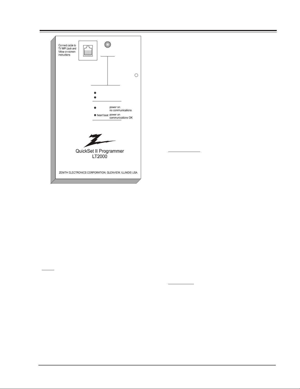
QUICKSET II PROGRAMMER
The Quick Set II programmer LT2000 (or LT1500) allow
custom setup and programming information to be quickly
copied from a master TV into multiple television sets.
The LT2000 can clone programmable labels, but the
LT1500 cannot. Once learned from the master, setup data
is retained in the LT2000 for future use and recall.
When using the LT2000, operation will be easier if the
TV is connected to a good quality signal and displaying
a stable picture. To operate the LT2000, use the indicated
keys on an installer’s remote or user’s remote, or the front
panel keys on the TV receiver.
SETUP
Begin the programming process by setting up a master
TV set using one of the installer’s remotes or an MBR
remote. Follow the instructions in the operating guide
for the specific TV model. Remember to set all features
that will be customized including the channel scan list,
channel labels, and installer menu setups.
Next connect the LT2000 to the master TV set using
the cable provided with the programmer. Connect the
cable between the MPI jack on the TV and the
programmer. The TV set automatically activates the
programmer.
Once connected, check the “Status Indicator” LED on
the programmer. If the indicator is green and flashing
(a double-blink “heartbeat” pattern), proceed to the
next step.
NOTE: A slowly flashing green light indicates there is
a problem with the communications between
TV and programmer. In this case, check for
damaged cable, poor contacts, or other
connection problems. If the status indicator is
red, the programmer batteries are low.
If communications are good, the sign-on screen will be
displayed on the TV screen as shown on the quick setup
instructions. If the intention is to set the TV’s or
programmer’s real-time clocks, and not the clone clock
or TV clock time settings, then press a key to proceed
to the main clone menu.
If a previously stored TV setup is in a particular clone
memory, it may be changed if desired by overwriting it
with a new setup. There is no need for a separated
memory clear operation. Setups stored in programmer
memory are nonvolatile and will be retained even after
a battery change.
LEARN FROM TV
Select “Learn From TV” then press ON/OFF, POWER, or
ENTER to begin learning process. Alternatively, use the
TV front panel CHANNEL UP or CHANNEL DOWN keys to
highlight choice. Press ON/OFF, POWER, or ENTER to
activate. The next screen will allow a choice of four
available memories to store this TV setup. Four different
TV setups can be stored in the LT2000.
Using the On-screen menu, choose a memory or choose
to return to the main selection menu. Now press ON/
OFF, POWER, or ENTER to activate your selection. The
next screen allows one last opportunity to check the
versions of TV and clone setups.
Press ON/OFF or POWER to activate the learning cycle,
or press any other keys to return to the selection menu
to make another choices.
Once a process has begun, the TV screen will display
“LEARNING IN PROGRESS”. Please wait for the process to
complete. When the TV screen displays “LEARNING
COMPLETED”, press any key to end the learning process
and return to the clone selection menu.
TEACH TO TV
Select “TEACH TO TV”, and then press ON/OFF, POWER,
or ENTER to begin teaching process. Alternatively, use
the TV front panel CHANNEL UP or DOWN keys to
highlight the choice and then press ON/OFF, POWER, or
ENTER to activate. The next screen displays a choice of
the four available memories that can be copied to the
TV. Select the desired memory number, and press ON/
OFF, POWER, or ENTER to begin the teaching process.
Alternatively, use the TV front panel CHANNEL UP or
DOWN keys to highlight choice. Press ON/OFF, POWER,
or ENTER to begin.
SR23 - 923-03509 1-9 CS - REMOTES
Page 16

REMOTE INFO
Using the on-screen menu, select a memory or return
to the main selection menu. Then press ON/OFF, POWER,
or ENTER to activate the selection.
The next screen allows for one last opportunity to check
the versions of TV and clone setups. Press ON/OFF or
POWER to activate the teaching cycle, or any other key
to return to the selection menu to make other choices.
Once a process has begun, the TV screen will display
the “TEACHING IN PROGRESS” message. Please wait for
the process to complete. When the TV screen displays
“TEACHING COMPLETED”, press any key to end the
teaching process and return to the clone selection menu.
SET CLONE CLOCK FROM TV
To set the real-time clock in the LT2000, select “SET
CLONE FROM TV” and then press ON/OFF, POWER, or ENTER
to copy current TV time to the clone clock. Alternatively,
use the TV front panel CHANNEL UP or CHANNEL DOWN
keys to highlight the choice. Then press ON/OFF, POWER,
or ENTER to activate.
This process will return the LT2000 to the sign-on screen
to display the clone and TV clock settings. Press a key
to go to the clone selection menu and perform other
functions, or simply disconnect if the time setting was
the last task.
SET TV CLOCK FROM CLONE
To set the real time clock in the, select “SET TV CLOCK
FROM CLONE” and then press ON/OFF, POWER, or ENTER
to copy current LT2000 time to the TV clock.
Alternatively, use the TV front panel CHANNEL UP or
CHANNEL DOWN keys to highlight the choice. Then press
ON/OFF, POWER, or ENTER to activate.
This process will return the LT2000 to the sign-on screen
to display the clone and TV clock settings. Press a key
to go to the clone selection menu and perform other
functions, or simply disconnect if the time setting was
the last task.
DISPLAY TV SETUP
Select “DISPLAY TV SETUP”, and then press ON/OFF,
POWER, or ENTER to begin the teaching process.
Alternatively, use the TV front panel CHANNEL UP or
CHANNEL DOWN keys to highlight your choice. Then press
ON/OFF, POWER, or ENTER.
The TV screen will display the items in the service menu
setups. Use this function to quickly check the TV for
correct setup. Press any key to clear display and return
to the clone selection menu.
DISPLAY CLONE SETUP
Select “DISPLAY CLONE SETUP” and then press ON/OFF,
POWER, or ENTER to begin the teaching process.
Alternatively, use the TV front panel CHANNEL UP or
CHANNEL DOWN keys to highlight the choice, then press
ON/OFF, POWER, or ENTER to begin.
The TV screen will display the memory selection menu.
Select the desired memory number, and then press ON/
OFF, POWER, or ENTER to display the contents of the
selected memory. Alternatively, use the TV’s CHANNEL
UP or CHANNEL DOWN keys to highlight the choice, then
press ON/OFF, POWER, or ENTER to begin.
The TV screen will display items in the factory menu
setup. Use this function to quickly check contents of a
particular clone memory for correct setup. Press any
key to clear the display and return to the clone selection
menu.
Note: The following two items only appear on sets
that do not have the built-in ability to clone
channel labels.
EDIT CHANNEL LABELS
Select the edit channel labels option and push ON/OFF,
Power, or Enter. Select the memory location (1,2,3,4)
and edit.
VOL L/R Selects update label
CH U/D Selects label to be changed
MUTE Clears present setting
ENTER Loads new labels
POWER Exits the menu
SEND CHANNEL LABELS
Select the send channel labels option and push ON/
OFF, Power, or Enter. Select the memory location
(1,2,3,4) and push ON/OFF. A message will indicate that
is doing the copy and when it is finished.
OPERATION NOTES
Disconnect the LT2000 from the TV set when the desired
task has been completed. Disconnecting the clone
automatically switches it off. The real time clock
continues to run when the main circuits are switched
off.
After replacing exhausted batteries, or if the programmer
behaves strangely after a static shock, use a paper clip
or similar instrument inserted through the small hole
marked “RESET” to activate the internal reset switch
and restore normal operation. After reset, check the
real-time clock setting. It may be necessary to reset
the clock from a TV programmed to the correct time.
The specific microprocessor used in any TV set may be
determined by activating the service menu. The
microprocessor part number appears at the top of the
screen with the service menu is activated. Processors
before the 221-01006 have limited screen display
capability. They cannot display entire screens as shown
in the quick setup instructions accompanying the
LT2000 programmer. Use the printed menu illustrations
on the quick setup sheet as an aid in making
programming choices.
SR23 - 923-03509 1-10 CS - REMOTES
Page 17
USER MENUS
USER MENUS 905-10533
SETUP MENU
The Setup Menu and all of the options for Presentation
Chassis are described below.
Note: This menu is not available while the set is in
computer mode.
SETUP MENU
AUTO PROGRAM
ADD/DEL/BLNK
CH. LABELS
CLOCK SET
CAPTIONS
ALARM
LANGUAGE
AUTO PROGRAM
The Auto Program feature automatically searches for all
available channels and marks them as ‘added’ so that
they may be accessed via the channel Up/Down key.
In the Auto Program screen:
• A message at the top displays “Auto Program” to
let the customer know that they have entered the
Auto Program feature.
• A line at the bottom of the screen shows that the
Up/Down and Left/Right Arrow keys are used for
Auto Program selections.
• The current RF input type (Off Air Antenna or Cable
TV) is highlighted. Use the Up/Down Arrow keys to
change the RF input type.
To start the Auto Program, press the Left/Right Arrow
key. If the Cable TV input type is selected, the Auto
Program routine will determine what type of cable system
is present.
Notes:
• Auto program clears all blanked channels, which were
added.
• While searching for channels, all keys except for the
Power key are disabled. This prevents an incomplete
Auto Program procedure.
• Running the Auto Program will clear the factory mode,
if it was active. This happens at the end of the Auto
Program.
• If the Auto Program line in the Setup Menu is ‘red’,
this indicates that the module did not pass one of
the test equipment’s tests.
TO PROGRAM
CHANNEL ADD/DEL/BLNK
After running the Auto Program, all channels found by
the Auto Program feature will be marked as ‘Added’.
However, some of these channels may be scrambled, or
undesired by the customer. The Channel Add/Del/Blnk
feature allows the customer to selectively mark any
channel as ‘Deleted’ or ‘Added’.
To change the status of a channel, press the Right/Left
Arrow key.
To change the channel while adding or deleting channels,
use the Channel Up/Down keys, or press the desired
channel digits followed by ‘Enter’. If Channel Up/Down
is pressed the next or previous channel, which was marked
‘Added’, will appear. If only one channel is present, to
change the channel the customer must use the digit
keypad to select a channel.
CH. LABEL
This feature allows the customer to select a channel label
for the current station. This channel label is displayed
in the Channel/Time display. Initially, all channel labels
are set to ‘——‘ (which means that auto label is selected).
To change the current channel label, press the Left or
Right Arrow key.
To change the channel while adjusting channel labels,
use the Channel Up/Down Arrow keys, or press the desired
channel digits, followed by ‘Enter’. (If Channel Up/Down
is pressed, the next or previous channel that was marked
‘Added’ will appear.)
Channel Labels
A&E CMTV ESPN HSE NOS TBN VC
ABC CNBC ESP2 HSN PBS TELE VCR
ACTS CNN ET IC PLAY TLC VH-1
ADC COM EWTN INSP PTL TMC VISN
AMC CSPN FAM JCN QVC TNN VJN
BCC CSP2 FNN LIFE RDS TNT WB
BET CTN FOX MAX REQ TRAV WGN
BRAV CTV F&V ME/U SC TSN WTBS
CA DIS FX MMT SCFI TVA WWOR
CBC DISC GALA MTV SHOW TWC YTV
CBN E! HBO NBC SIN UPN - - - CBS ENC HN NICK TBS USA None
NOTE:
Selecting the "- - - -" label option means
that auto label is selected. Selecting the
"None" option means the channel will not
have a label.
If no channels are found then the following message
will appear: “Make sure that the cable/ant. is connected
and try again.”
SR23 - 923-03509 1-11 CS - MENUS
Page 18

USER MENUS 905-10533
Notes:
• When the “- - - -” label is selected, then the Auto
channel label is activated, in other words, the program
automatically takes the channel label of the signal
that is sent by broadcasting through the XDS service.
• If the label None is selected, the Auto channel label
is not activated.
PROGRAMMABLE CHANNEL LABELS
Besides the labels already provided, the customer may
select a label of his or her choice. The programmable
labels are at the end of the list of labels already provided.
Pressing the volume key allows the editing of the first
character. In this case it is the “L” that would start
blinking. However, if the Left volume key is pressed, the
“1” is the character that would begin to blink. When the
character begins to blink, the customer may select
another character.
The method of selecting another character is by pressing
the channel Up/Down key. If the channel up key were
pressed, the character displayed would be an “M”. On
the other hand, if the channel down key is pressed, the
character displayed is an “L”.
There are 20 programmable labels that the customer may
program. The available characters to choose from are
the following:
Programmable Channel Labels
Blank ê Reserved - < K Z i x
|î Reserved.=L[jy
| ô Space / > M \ k z
Blank û ! 0 ? N ] l {
Òá “ 1@O^m|
°é # 2AP_n}
½í $ 3BQ‘o~
¿ó % 4CRapBlock
äú & 5DSbq
¢V ‘ 6ETcr
£¸ ( 7FUds
)8GVet
àñ * 9HWfu
èReserved+ :IXgv
âReserved‘ ;JYhw
• Any changes done to a label are stored even if another
keystroke occurs. For example if the customer is
programming a label and the first 3 letters are entered
and accidentally the ENTER key is pressed or the Menu
key is pressed, the label is stored with only the three
characters being changed. The other two remain
unchanged. The programmable labels have 5
characters that may be programmed.
• If, for example, the 10th label is programmed as ABCDE,
then the customer decides to clear it. The channel
automatically receives the label NONE and label 10 is
restored to LAB10.
• Using the Channel Up/Down the customer may select
the above-mentioned characters.
CLOCK SET
This Setup Menu Line allows the customer to set the
clock time and date.
When no time is set, the display shows: - -: - There are two ways to set the time:
1. Direct Entry is preferred. Use the digit keys, followed
by ‘Enter’ or Select Up/Down.
2. Left/Right Arrow keys.
When the first digit is introduced, the display shows:
0:0d AM
When the time is set, the display shows:
hh:mm AM
where d = digit, mm = minutes, and hh = hours.
To select either AM or PM, the Timer key must be used.
Pressing the Timer key, toggles AM and PM to allow the
customer to select AM or PM.
Notes:
• Entering the time in 24 hour (Military) format is
allowed. AM/PM will be toggled automatically.
• Entering an invalid time (“0” for example) will result
in the clearing of the current time - - : - -.
• When only one digit is pressed and no other is pressed
in an interval of seven seconds, the current time will
be cleared.
CAPTION
This function allows the user to show in the screen the
configuration menu to captions.
Notes:
• If the mute key is pressed, the label is cleared. The
channel is automatically given the label NONE.
SR23 - 923-03509 1-12 CS - MENUS
Page 19
USER MENUS 905-10533
BRIGHTNESS
COLOR
TINT
VIDEO MENU
CONTRAST
PICTURE PREF PRESET
SHARPNESS
ALARM
If the factory menu item Alarm is set to 1 the Alarm
feature is activated.
SETUP MENU
AUTO PROGRAM
ADD/DEL/BLNK
CH. LABEL
CLOCK SET
CAPTIONS
ALARM
LANGUAGE
TO SET ALARM
LANGUAGE
This feature allows the customer to change the menu
language from English, Spanish, or French by pressing
the Left/Right Arrow keys.
AUDIO MENU
All options in the Audio Menu are selected with the Up
Arrow key. Once the option is selected, use the Left/Right
Arrow keys to adjust to option to the desired setting.
AUDIO MENU
BASS
TREBLE
BALANCE
AUDIO MODE
SOUNDRITE
FRONT SURR
SPEAKERS
AUDIO PREF
STEREO
OFF
ON
ON
PRESET
If 2nd Audio/SAP is selected, but the current channel
does not support SAP, then either Stereo or Mono will be
heard.
SOUNDRITE
The SoundRite feature is used to obtain a uniform volume
level, particularly while changing channels. The SoundRite
feature can be best demonstrated on a channel with no
signal (snow).
FRONT SURROUND
Front Surround sound can be set to ‘ON’ or ‘OFF’, regardless
of the current Audio Mode setting. However, the surround
effect can only be heard when the Audio Mode has been
set to ‘Stereo’ and a Stereo signal is present. When this
condition exists, there will be a short mute (200ms)
while toggling the Surround ‘On’ to ‘Off’, to embellish
front surround activation.
SPEAKERS
The Speaker feature is used to turn the internal speakers
on or off. It does this by pulling the power amp mute
line.
AUDIO PREF
This feature allows the customer to maintain two separate
audio settings by selecting “custom” or “preset”. The
Factory gets the “Preset” setting and the customer sets
“custom”. The PRESET and CUSTOM settings are selected
using the Left/Right arrow keys.
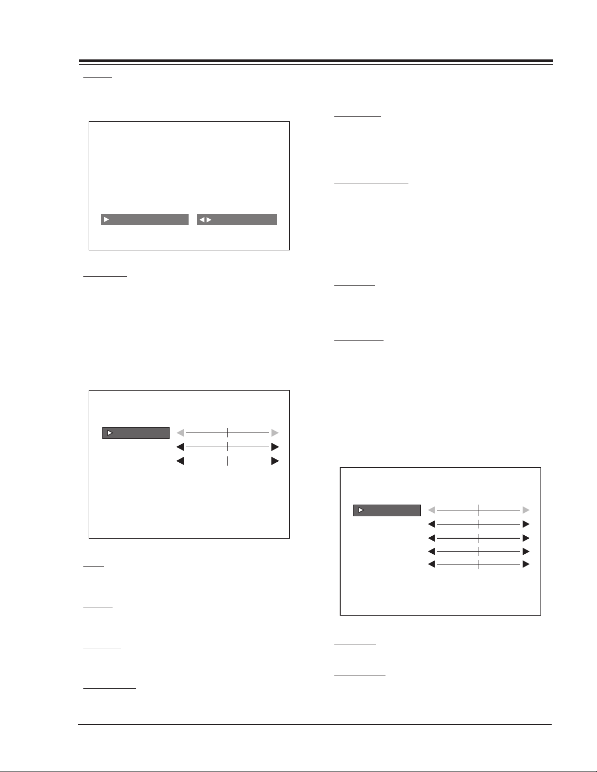
VIDEO MENU
All menu items are adjusted with the Left/Right Arrow
keys. Each option of the Video Menu is shown below:
BASS
Bass adjustment has 15 steps (0 to 14). A center mark
indicates step 7.
TREBLE
Treble adjustment has 15 steps (0 to 14). A center mark
indicates step 7.
BALANCE
Balance adjustment has 29 steps (0 to 28). A center
mark indicates step 14.
AUDIO MODE
There are three audio modes available: Mono, Stereo, 2
Audio/SAP.
SR23 - 923-03509 1-13 CS - MENUS
CONTRAST
Contrast adjustment has 64 steps (0 to 63).
BRIGHTNESS
Adjusts the brightness of the picture.
nd
Page 20

USER MENUS 905-10533
COLOR
Color adjustment also has 64 steps (0 to 63).
TINT
Tint Adjustment has 64 steps (0 to 63). A center mark
indicates step 29.
SHARPNESS
Sharpness adjustment has 64 steps (0 to 63). The
sharpness value is sent to the video processor as Custom
Sharpness.
PICTURE PREF
This feature allows the customer to maintain two separate
Contrast, Brightness, Color, Tint, Sharpness setting
“Custom” and “Preset”. The factory sets the “Preset”
setting and the customer sets “Custom”. The PRESET and
CUSTOM settings are selected using the Left/Right Arrow
keys.
PARENTAL CONTROL
The Parental Control Menu items are selected with the
Up/Down Arrow keys. Once the option is selected, use
the Left/Right Arrows keys to set each of the option.
Note: The Parental Control Menu is not available while
in computer mode.
AUXILIARY SOURCES
To block or unblock the sources, press the Left/Right
Arrow key.
PARENTAL CONTROL
Use the Left/Right Arrow keys to select the Age Block
Menu.
AGE MENU
GENERAL
CHILDREN
PRESS CC TO RETURN
UNBLOCKED
GENERAL BLOCK
Once entering into the Age Block Menu, the customer
has the option to block channels for general age or to
block channels for children.
To block channels for a general age, the customer may
either select: UNBLOCKED, TV-G AND ABOVE, TV-PG AND
ABOVE, TV-14 AND ABOVE or TV-MA.
CHILDREN BLOCK
To block channels for children, select either: Unblocked,
TV-Y AND ABOVE or TV-Y7.
CONTENT BLOCK
Use the Left/Right Arrow keys to select the Content Block
Menu.
AUX SOURCES
MPAA RATING
AGE BLOCK
CONTENT BLOCK
SET HOURS
SET PASSWORD
LOCK ON/OFF
Note: The SOURCE key may be used to view the video
BLOCKED
CONTENT BLOCK
DIALOG
LANGUAGE
SEX SCENES
VIOLENCE
F VIOLENCE
NO RATING
PRESS CC TO RETURN
UNBLOCK
source.
MPAA RATING
The MPAA selector allows the customer to select either
to have the channel Unblocked, G AND ABOVE, PG AND
ABOVE, PG-13 AND ABOVE, R AND ABOVE, NC-17 AND
DIALOG BLOCK
To block the dialog, use the Left/Right Arrow keys to
select either: Unblocked, TV-PG AND ABOVE or TV-14.
ABOVE, or X.
LANGUAGE BLOCK
AGE MENU
SR23 - 923-03509 1-14 CS - MENUS
Page 21

USER MENUS 905-10533
To block the dialog, use the Left/Right arrow keys to
select either: Unblocked, TV-PG AND ABOVE, TV-14 AND
ABOVE, or TV-MA.
SEX SCENES BLOCK
To block the Sex Scenes, use the Left/Right Arrow keys
to select either: Unblocked, TV-PG AND ABOVE, TV-14
AND ABOVE, or TV-MA.
VIOLENCE BLOCK
To block the Violence, use the Left/Right arrow keys to
select either: Unblocked, TV-PG AND ABOVE, TV-14 AND
ABOVE, or TV-MA.
F VIOLENCE BLOCK
To block the F Violence, use the Left/Right Arrow keys
to select either: Unblocked, TV-Y7.
NO RATING
To block No Rating, use the Left/Right Arrow keys to
select either: Unblocked and Blocked.
SET HOURS
Use the Left/Right Arrow keys to adjust the number of
hours the Parental Control feature will be active.
RE-ENTERING PARENTAL CONTROL MENU
If the Parental Control feature has been activated, the
software will not allow immediate entry into the Parental
Control Menu. Instead, it will prompt for the correct
password.
If the correct password is entered, the Parental Control
menu will appear, with the highlighted item “Lock On/
Off”, which assumes that the customer most likely wants
to turn the feature off. If an incorrect password is entered,
an error message (“Not Accepted!”) appears, and will
not disappear until 5 seconds has elapsed. This extended
time provision increases the amount of time necessary
for a child to “crack” the password.
RE-ENTERING PARENTAL CONTROL
PASSWORD?
ENTER CODE: __
SET PASSWORD
Press the Left/Right Arrow key to allow setting a
Password.
TO ENTER PASSWORD
The software accepts four-digit codes only. The customer
must enter a password.
REPEAT PASSWORD
After a four-digit code has been entered, the software
requires the customer to re-enter the same four-digit
code.
PASSWORD NOT ACCEPTED
If an invalid code is entered, or the two codes entered
do not match, an error message (“Not Accepted!”) will
appear blinking.
Note: This error message also appears when no code is
entered for the password or if only one digit is
entered and no other digit has been entered.
LOCK ON/OFF
This item turns the Parental Control feature on or off.
The Ctrl. feature can only be turned on if the hours > 0,
and a password has been set. Otherwise the Lock On/
Off line will display either of the following error
messages: “Must Set Hours” or “Must Set Password.”
Notes:
• The Parental Control menu will remain up for 15
seconds after the last key press.
• The QUIT key may be pressed to remove the Parental
Control menu if the actual channel source is blocked.
DISPLAY WHEN PARENTAL CONTROL IS ACTIVE
When the Parental Control is active and the channel is
blocked, the display on the screen shows two lines. The
first line displays a message saying that the “PARENTAL
LOCKOUT IS ACTIVE.” The second line displays the amount
of time (in hours) left in the lockout.
SR23 - 923-03509 1-15 CS - MENUS
Page 22
USER MENUS 905-10533
CH 4
3:35 PM
MONO
SOURCE
FRONT COMPUTER SVGA
Parental Lockout Is Active
01:23 Hours Remaining
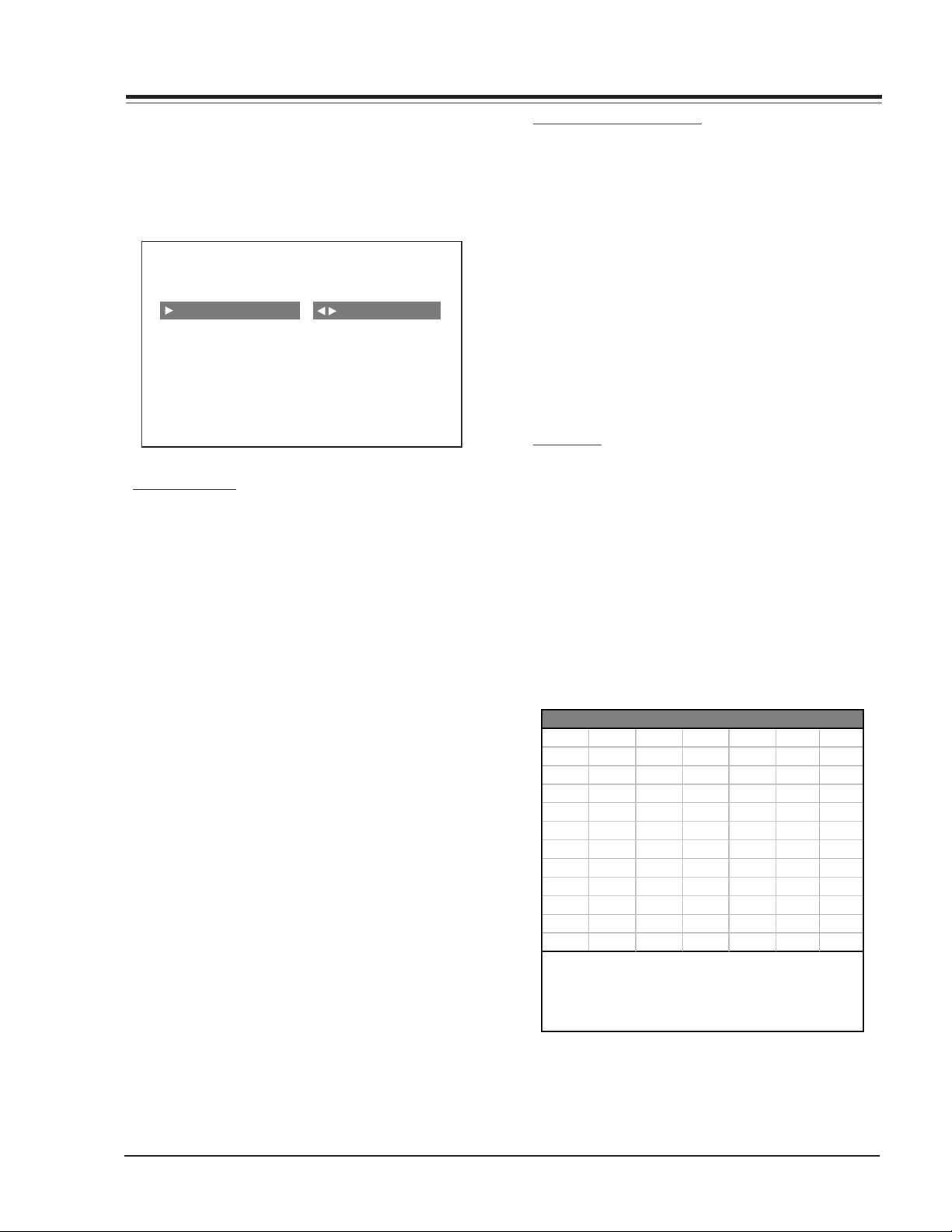
SOURCE MENU
This option allows the user to select the source they
desire, which determines the signal that feeds the video
processor, the options are: ANTENNA/CABLE, AUX VIDEO
or VIDEO, CAMPORT, FRONT COMPUTER SVGA, REAR
COMPUTER SVGA, and REAR COMPUTER NTSC OUT.
Use the arrow keys and the ENTER key for signal switching.
SOURCE MENU
ANTENNA/CABLE
CAMPORT
AUX VIDEO
S-VIDEO
FRONT COMPUTER SVGA
REAR COMPUTER SVGA
REAR COMPUTER NTSC OUT
PRESS TO CHANGE.
PRESS OR <>KEYS TO ACTIVATE
ENTER
PRESS:
SOURCE TO CHANGE SOURCE
ENTER TO SELECT SOURCE
To select a Source, press the Source Key and source menu
appears (as shown below) showing the present source.
Pressing the Source key again, switches to the next source
but the input signal does not change. Once the desired
source is found, pressing the ENTER key selects that source
and changes the input. If ENTER is not pressed in
approximately 15 sec. The source menu turns off.
Note: If any one of the three computer sources is selected
and no computer is connected to the source, the
following screen will appear:
F COMP SVGA
1:51PM
STEREO
PLEASE CONNECT A COMPUTER
800 X 600, 60HZ
SOURCE MENU
ALTERNATE SOURCE MENU BY TV/SOURCE KEY
Same as source menu, but using the TV/SOURCE Key.
Note: CAMPORT (#33) and FRONT COMPUTER SVGA (#209)
are only available when the Auto-Sense feature
for either has been disabled in the Factory Menu.
SR23 - 923-03509 1-16 CS - MENUS
MUTE
When the Mute key is pressed, the speakers will be turned
off.
MUTE WITH CHANNEL DISPLAY
When the mute key is pressed and the channel display
is on, the following display appears:
Page 23

USER MENUS 905-10533
CH 4 HBO
3:35 PM
MUTED
MUTE WITHOUT CHANNEL DISPLAY
When the mute key is pressed and channel display is
off, the following display appears:
MUTED
CH 14 HBO
3:35 PM
MONO
FUNCTION NOT AVAILABLE DISPLAY
When the Time has not been set yet, and the customer
wants to enter the Alarm Menu, there will be an error
notification stating that the function is not available.
CHANNEL TIME DISPLAY
When the ENTER key is pressed the TV display will appear.
The following is an example of the display screen:
The first line is the channel and the label (if one has
been selected for the channel). The second line, displays
the time. The third line displays the Audio mode (Mono,
Stereo or SAP).
FUNCTION NOT AVAILABLE
PARENTAL CONTROL PASSWORD IS RESET DISPLAY
To reset parental control, press & hold the MENU key
until the Channel/Time display appears, then press ‘9’,
‘8’, ‘7’, ‘6’, and CC. The following menu appears after the
parental control is reset:
SR23 - 923-03509 1-17 CS - MENUS
Page 24

USER MENUS 905-10533
PARENTAL CTL PASSWORD IS RESET
DISCONNECT FRONT A/V JACKS DISPLAY
If the channel Up/Down keys are pressed and Auto
Camport in the Factory Menu (#33) has been enabled
and there is a device connected to the front Camport,
the following message appears:
keys. Same as the Video Menu for a RF signal.
This feature allows the customer to maintain two
separate Contrast, Brightness, Color, Tint, and Sharpness
settings “Custom” and “Preset”. The factory sets the
“Preset” setting and the customer sets “Custom”. The
PRESET and CUSTOM settings are selected using the Left/
Right Arrow keys.
PARENTAL CONTROL
(For Video Source Input)
The Parental Control Menu items are selected with the
Up/Down Arrow keys. Once the option is selected, use
the Left/Right Arrows keys to set each of the option.
Notes:
• This Parental Control is the same as the Parental
Control for the Ant/Cable source input.
• Also, There is no Parental Control Menu when the
input source is any of the Computer sources.
CAPTIONS SETUP
The caption setup items are selected with the UP/DOWN
arrow keys. Once the option is selected, use the Left/
Right arrows keys to set each option.
DISCONNECT FRONT A/V JACKS
VIDEO SOURCE INPUT
CUSTOM FEATURES
(For Video Source Input)
Same as Setup Menu for an RF signal.
AUDIO MENU
(For Video Source Input)
Same as Audio Menu for an RF signal, except auto mode
is not available.
VIDEO MENU
(For Video Source Input)
All menu items are adjusted with the Left/Right Arrow
CAPTION SETUP
OPER MODE
SEL CC TYPE
CC CAPTION
CC ON MUTE
CAPTION LOCK
PRESS ENTER TO CHOOSE
PRESS ADJ TO CHANGE
QUICK/MUTE
Note: When the user selects the quick/mute operation,
if the cc key is pressed, the next message is
displayed.
OPERATION MODE
Toggle “between” quick/mute operation or standard
operation.
SELECT CC TYPE
In this option the user can select the type of captions
used. The caption types available are: caption1, caption
2, caption3, caption4, Text1, Text2, Text3, and Text4.
CC CAPTION
This option switches the caption selected in “select cc
type” ON or OFF.
CC ON MUTE
SR23 - 923-03509 1-18 CS - MENUS
Page 25
USER MENUS 905-10533
This option enables the captions when the TV is muted.
CAPTION LOCK
This option stores the caption configuration in EEPROM.
It also is used to remember the last configuration of
the captions.
COMPUTER SOURCE INPUT
AUDIO MENU
(For Computer Source Input)
Same as Audio Menu for a RF signal, except audio mode
is not available.
VIDEO MENU
(For Computer Source Input)
All menu items are adjusted with the Left/Right Arrow
keys. Each option of the Video Menu is shown below:
VIDEO MENU
CONTRAST
BRIGHTNESS
COLOR
TINT
SHARPNESS
PICTURE PREF PRESET
or 4 steps up from the value set in the Factory Item
153 GREEN DRIVE SVGA.
If this factory menu item is set at 30, the Green
adjustment in the Video Menu allows the Green Offset
to be set at –4 or +4 of the default value. Below is the
Menu item.
BLUE ADJUSTMENT
The Blue adjustment allows the customer to adjust
the Blue for Comp. SVGA or NTSC. To accomplish this
the Blue adjustment can be adjusted 4 steps down or
4 steps up from the value set in the Factory Item 155
BLUE DRIVE SVGA. If this factory menu item is set at
30, the Blue adjustment in the Video Menu allows the
Blue Offset to be set at –4 or +4 of the default value.
Below is the Menu item.
HORIZONTAL POSITION
The Horizontal Position adjustment has 64 steps (0 to
63). This Video Menu item allows the adjusting of the
Horizontal Position of the screen.
VERTICAL POSITION
This Video Menu item allows the adjusting of the Vertical
Position of the screen.
HORIZONTAL SIZE
The horizontal size adjustment allows customer to
adjust the Horizontal size for Comp. SVGA or NTSC.
Factory reference is 179.
CONTRAST
Contrast adjustment of the picture has 64 steps (0 to
63).
BRIGHTNESS
Adjusts the brightness of the picture.
RED ADJUSTMENT
The Red adjustment allows the customer to adjust the
Red for Comp. SVGA or NTSC. To accomplish this the
Red adjustment can be adjusted 4 steps down or 4
steps up from the value set in the Factory Item 153
RED DRIVE SVGA. If this factory menu item is set at
30, the Red adjustment in the Video Menu allows the
Red Offset to be set at –4 or +4 of the default value.
Below is the Menu item.
GREEN ADJUSTMENT
The Green adjustment allows the customer to adjust
the Green for Comp. SVGA or NTSC. To accomplish this
the Green adjustment can be adjusted 4 steps down
VERTICAL SIZE
The vertical size adjustment allows customer to adjust
the Vertical size for Comp. SVGA or NTSC. Factory
reference is 190.
PICTURE PREF
The Picture Preference allows the customer to adjust
all the items of the Video Menu or to select Preset
values.
REMOTE CONTROL FUNCTIONS
The customer has the option to use the remote control
to activate certain functions from the OSD.
Notes:
• Use a full screen computer display with high average
brightness for best results.
• Auto Size will adjust the computer image to match
the TV screen.
• The image cannot be zoomed in Freeze Mode.
As with the Remote Key Command Functions, menus
are operated through the Numbered Keypad. Generally
speaking, keys 4 and 6 adjust menu options, key 8
cycles through menus and key 5 cancels all operations
no matter what menu is being are adjusting.
SR23 - 923-03509 1-19 CS - MENUS
Page 26
USER MENUS 905-10533
G
G
s
Remote Functions
KEY NORMAL MODE MENU MODE ZOOM MODE
1 Enter Zoom Mode N/A Cancel Zoom Mode
2N/A N/A Pan Up
3 Compress On/Off N/A Compress On/Off
4 N/A Menu Adjust Pan Left
5 Enter Menu Mode Cancel Menu Mod e Enter Menu Mode
6 N/A Menu Adjust Pan Right
7 Begin Auto-Size N/A Begin Auto-Size
8 N/A Menu Select Pan Down
9N/A N/A N/A
0 Freeze N/A Freeze
Remote Key Command Functions
Screen Size
8
6
Manual Set
8
6
Advanced
6
SETTING
Out h-Centre
Out H-Wid th
Out V-Centre
Out V-Height
VGA Left
VGA Width
VGA Top/4
VGA bottom/4
Sense Level
Clk Width
8
Limits of Settings
RANGE
65 to 85
80 to 120
107 to 232 for NTSC, 300 to 400 for SV
200 to 250 for NTSC, 480 to 600 for SV
0 to 20
30 to 81
0 to 40
70 to 260 (i.e. up to 200 *4 = 800line
1 to 3
0 to 3
Out H Centre
Adjust
8
6
4
4
VGA Left
Adjust
8
6
Out H Width
Adjust
4
VGA Bot
Adjust
4
Store Settings
VGA Width
6
8
6
8
6
8
4
Sense
4
Store Settings
Adjust
8
8
8
6
6
6
Clk Width
4
Out V Height
4
Vert Freq
8
Adjust
8
8
6
6
4
Rev #
8
VGA Top
Adjust
8
Eng. Reset
8
6
6
Out V Centre
Screen Size
4
VGA Lines
6
8
8
SR23 - 923-03509 1-20 CS - MENUS
Page 27

SECTION 2
SERVICE MENU
SERVICE MENU
Access the Installer’s Menu by using the remote control
or the keyboard on the front of the set. With the remote:
Press & Hold MENU key until the Channel/Time display
appears, then press 9, 8, 7, 6, and ENTER.
Press and hold MENU key until the Channel/Time display
appears. Simultaneously press the ADJUST Right and
CHANNEL Up keys. To exit Installer’s Menu, press ENTER.
Notes:
• When the factory mode is set to “1”, then
press ‘9’, ‘8’, ‘7’, and ‘6’, followed by
‘ENTER’ to access the Installer’s Menu.
• To reset parental control press & hold the MENU key until
the Channel/Time display appears, then press ‘9’, ‘8’,
‘7’, ‘6’, and CC .
00 F Mode: Use the Select key to select item #00, which
is the first item in the Installer’s Menu. The Factory
Mode item should always be left off (Zero is off). When
left in this mode, only items from 0 to 27 are visible.
When the factory mode is set to 1, all menu (Audio or
Video settings) items will be available. Also they will
appear on the screen one at a time at the top left of
the screen.
When The Factory Mode is on, the Factory Menu line
appears at the top of the screen to allow for proper
setting of the video.
1391 - P07 01.44 02
Microcontroller
part number
4 VERT POS 15
SN : 0121-41362000
UPN : 065-054-032-000
01/29/02 TE=10110000
Build Date
Program
Revision
Factory Option
When the Factory Mode is turned off, all TV functions
are returned to normal. The dashes on the menus are
removed indicating that the Factory Mode is off. There
are 4 ways to turn off the Factory Mode:
Font
Revision
Te Status
AC power.
• Auto off enabled: The Auto Off feature is always enabled,
regardless of the state of the “Auto OFF” Factory Menu
item.
• Settings Displayed in Customer Menus: When adjusting a
bar graph setting in the Video and Audio Menus, a number
is displayed showing the actual numeric value stored in
EEPROM for that setting. On menu items without a bar
graph setting, two dashes indicate that the Factory Mode
is on.
• Video Preference Settings Inhibited: In the Video Menu,
the Custom Video Preference settings are inhibited while
the Factory Mode is on and will NOT be stored in EEPROM.
(This allows the factory to temporarily change the settings
and not store them permanently.)
01 Preset Px: Used to store the customer menu adjust-
ments in the nonvolatile memory of the EAROM. Settings for Contrast, Brightness, Color and Tint are stored
in this manner. 0 is Custom and 1 is Preset.
02 Preset Ax: Saves your custom audio settings (Bass,
table, balance, audio mode, Soundrite, front surround,
speaker) in nonvolatile memory (not affected by power
loss). Memory status is indicated by a 1 for “custom
settings already stored”, or 0 for “custom settings have
not been stored.”
03 Power Manage: Used for saving energy. When set to
0, Power Manage is off. The number represents the
hours that the TV will remain on, unless there has been
activity from either the control panel or remote.
04 Vert Pos: Moves Captions and displays vertically on
the screen. Use the ADJUST keys.
05 Horz Pos: Moves Captions and displays horizontally
on the screen. Use the ADJUST keys.
06 Band/Afc: There are 8 possible settings for this op-
tion.
1. Change Installer’s Menu Item “00 F Mode” to 0.
2. Run Auto Program.
3. Use the Clock Set feature to set the time.
4. Use Factory off IR code.
0 = Broadcast Fixed 4 = Broadcast AFC
5 = CATV Fixed 1 = CATV AFC
6 = HRC Fixed 2 = HRC AFC
7 = ICC Fixed 3 = ICC AFC
Notes:
• AC Power on Enabled: The ‘AC Power on’ feature is always
enabled, regardless of the state of the “AC on” Installer’s
Menu item. The set will automatically turn on when AC
power is applied. The POWER key will not turn the set
off. The only way to turn off the set is by removing the
07 Min Volume: Determines the minimum volume level
allowable with the VOLUME (VOL) Up/Down Control.
In this way, for example, someone cannot set the volume too low to hear. The factory default is 0, which
provides full range of volume control. It may be best
to set the same value on every TV.
SR23 - 923-03509 2-1 CS - SERVICE MENUS
Page 28

SERVICE MENU (continued)
Note: The minimum volume level cannot have a value setting
higher than in the MAX VOLUME level (described
below).
08 Max Volume: Determines the maximum volume level
allowable with the VOLUME (VOL) Up/Down Control.
In this way, for example, someone cannot set the volume level high enough to disturb others. The factory
default is 63, which provides full range of volume control. It may be best to set the same value on every TV.
Note: The maximum volume level cannot have a value setting
lower than in the MIN VOLUME level (described above).
09 AC on: Allows the TV to turn ON just by applying AC
power. Pressing the ON button is not necessary. This
is desirable when the TV is plugged into a cable box
or a power outlet controlled by a wall switch. Use adjust to select 0 or 1, where 0 is OFF and 1 is ON.
Note: When set to 1 (ON), the TV does not respond to ON/
OFF commands from either the remote or the control
panel, and the SLEEP TIMER is also nonfunctional.
10 Key Defeat: When set to 1, it prevents the end user
from accessing screen menus on the front panel keys,
SELECT and ADJUST do not function. When set to 0,
those keys are functional. The menus can always be
accessed with MENU on the remote.
11 Strt Ch: When active, this function allows you to set
the initial volume level setting and channel number
when the TV is turned ON. This feature is useful for an
in-house information channel, since the TV would always select that channel when it is turned on. When
inactive, the volume level and channel retain the settings when the set was last used.
The range of values is 0-255. Use the ADJUST keys to
choose. With number 255 the feature is inactive. Other
numbers determine the start channel. Set the volume
level as desired before exiting the service menu. 0 is
the “AUX” channel.
Generally, this feature is used in connection with START
CHAN/VOL where the start channel may, for example,
be set to 3 or 4. If the start channel is 3 then the TV
will remain on channel 3.
15 Ghost Ch: When set to 1, the current channel number
is displayed in the upper right corner of the CRT. The
number moves slightly to prevent damage to the
screen. The default is “0” or OFF. When captions are
on, the “ghost” channel is not displayed.
16 Not Used
17 Text Mode: Determines whether TEXT 1 and TEXT 2
decoding is enabled when CAPTIONS are turned on (either from the Setup Menu or directly with CC on remote). When set to 1, only Caption 1, 2, 3, and 4 are
enabled. When set to 2, Caption 1, 2, 3, and 4 and
Text 1, 2, 3, and 4 are enabled.
18 Sleep Timer: When set to 1, a end-user may set the
SLEEP TIMER feature (but no message is displayed prior
to turnoff). When set to 0, the sleep timer is not available.
19 Alarm: Gives you the option of making the alarm func-
tion available to the end-user. Set to 1, alarm function is available. Set to 0 to withhold this function.
20 Ch. Over Ride: When set to 1, the user is allowed to
select channels with either Channel Up/Down or by
direct keypad entry. When set to 0, only those channels that are entered for scanning may be selected.
21 Old Ocv: Set to 1 for operation with “SpectraMate”
systems from on command corporation.
22 Caption Lock: Set to 1 to restore previous caption
on/off state after the TV turns off when set to 0, captions are always off when TV is initially turned on.
23 Function Pre: Set to 1 to suppress channel prev screen
and enable user function menu with some pay per view
systems.
12 Strt Vol: When active, this fuction allows you to de-
termine the initial volume level setting when the TV is
turned on. This feature is useful for an in-house information volume, since the TV would always select that
volume when is turned on. When inactive, the volume
level retain the settings when the set was last used.
13 Not Used
14 Chan Lock: When set to 1 the CHAN LOCK is ideal if a
cable box (or similar) is the sole source for programming and the TV must always be on the same channel.
Changing channels with the Channel Up/Down or keypad numbers is impossible. Channel Lock is inactive
when set to 0 (default).
SR23 - 923-03509 2-2 CS - SERVICE MENUS
24 Feature Level: Set to 1 to see Zenith Code, when set
to 0 Private Codes are shown.
25 NTSC ScanCard: Set to 1 to instate TV ONE card in
NTSC mode.
26 Not Used
27 Mute disable: This function disable the mute opera-
tion in the TV. Also applies for MPI operation.
28 V-Chip: Enable/Disable the V-CHIP.
29 Max Block Hrs: Enable the V-CHIP maximum block
time.
30 Strt Aux Srce: Enable the initial AUX when is ac-
cessed with Up/Down key or 999.
Page 29

SERVICE MENU (continued)
FACTORY MENU ITEMS
31 Mute time: Time during the TV stays in blank state
when Real Time= Mute Time * lbms the switching is
between sources.
32 Y/C Loop out: Enable/Disable the Y/C out of the rear
Jack Pack.
33 Auto Camport: Enable/Disable the Camport Auto De-
tect.
34 Not Used
35 A Att: Adjust the signal level input to COMPIN (Pin
19) to the standard input level. Variable range of the
input signal: 245 mVrms –5.0 dB to +3.0 dB. 0 = Level
min. and 15 = Level max.
36 A Vco: Adjust STEREO & SAP VCO free running fre-
quency (fo). Variable range: fo ±20%. 0 = Free running frequency min, 63 = Free running frequency max.
37A Filter: Adjust the filter fo of the ST, SAP and dbx
blocks. Variable range: fo ±20% 0 = Frequency min,
63 = Frequency max.
38 A Spectral: Perform high frequency (fs= 3 kHz) sepa-
ration adjustment. 0 = Level max, 63 = Level min.
39 Wide Band: Perform low frequency (fs= 300 Hz) sepa-
ration adjustment. 0 = Level min, 63 = Level max.
NTSC IC 221-1377 FROM 40 TO 61
40 Hue: Hue Control. Range: 0-63, 0 = Flesh color ap-
pears red, 63 = Flesh color appears green.
41 Dpic off: Y black expansion ON/OFF switch. Range: 0-
1, 0 = ON, 1 = OFF.
42 Color: Color control. Range: 0-63, 0 = Minimum 63 =
Maximum.
43 Canal: When this register is set to “1”, the first and
last 3H of the video are replaced by DC during YUV
output. Range: 0-1, 0 = No video portion DC replacement, 1 = DC replacement.
44 Sharpness: Sharpness control. Range: 0-1, 0 = Mini-
mum, 15 = Maximum.
45 Sub Cont: Sub contrast adjustment. Range: 0-15, 0 =
Minimum, 15 = Maximum.
46 Sub Hue: Hue center adjustment. Range: 0-15, 0 =
Flesh color appears red, 15 = Flesh color appears green.
47 Sub Color: Color center adjustment. Range: 0-15, 0 =
Minimum, 15 = Maximum.
48 C-Trap Adj: Chroma trap adjustment. Range: 0-15, 0
= High, 7 = Center, 15 = Low.
49 Afc: AFC loop gain selector. Range 0-15, 0 = AFC loop
gain high, 1 = AFC loop gain medium, 2 = AFC loop
gain low, 3 = AFC loop open, free-running mode.
50 Trap on: Y system chroma trap ON/OFF. Range 0-1, 0 =
OFF, 1 = ON.
51 Tot on: Chroma TOT filter ON/OFF. Range 0-1, 0 = OFF,
1 = ON.
52 Y Drive: Y output gain control. Range: 0-31, 0 = -
6.3dB, 31 = +3.5dB.
53 Shp-F0: Sharpness f0 selector. Range: 0-1, 0 = 3Mhz,
1 = 1.5Mhz.
54 Cd Mode2: V sync. signal pull-in speed selector Range:
0-1, 0 = Standard 1 = High speed.
55 U Ped: DC control of pedestal portion of U output
(for video). Range: 0-15, 0 = -35mV, 7 = Center, 15 =
+40mV.
56 V Ped: DC control of pedestal portion of V output (for
video). Range: 0-15, 0 = -35mV, 7 = Center, 15 =
+40mV.
57 Dc Tran: DC transmission ratio setting. Range: 0-7, 0
= Maximum (100%), 7 = Minimum (78%).
58 Pre Over: Sharpness preshoot/overshoot ratio set-
ting. Range: 0-3, 0 = 1:1 (pre:over), 3 = 4:1 (pre:over).
59 Abl Cent: ABL center voltage control. Range: 0-3, 0 =
Minimum, 3 = Maximum.
60 Abl: ABL gain control. Range: 0-1, 0 = Standard, 1 =
Low.
61 Delay: Allows the following delay times to be added
to the Y signal. Range 0-3, 0 = 0nS, 1 = 60nS 2 =
120nS, 3 = 180nS.
NTSC IC 221-1376 FROM 62 TO 111
62 Akb-T: Selection of timing pulse, which generates
reference pulse (Set to NORMAL mode at power on).
Range 0-1, 0 = NORMAL mode (reference pulse generated by SCP input only), 1 = V compression mode (reference pulse generated from VTIM-IN,HP-IN).
63 Blksw: Selection of H, V blanking system for RGB-OUT
(Set to 0 at power on). Range: 0-1, 0 = Normal blanking mode (blanking up to VCE(sat) level, 1 = Blanking
at value set by BLK-BOTTOM (Refer to the description
of the BLK-BOTTOM register).
64 Mat-Out: Selection of type matrix conversion; selected
signal is output from pins 76,77 and 78. A DC voltage
of approximately 4V is output only for 3 of these
modes. Range 0-3, 0 = THROUGH1 (when YCbCr is input, normal NTSC input), 1 = Matrix of YPbPr to YCbCr
signal, 2 = Matrix conversion of GBR to YCbCr signal, 3
= THROUGH2 (GBR is input directly to internal RGB
system, SVGA input).
SR23 - 923-03509 2-3 CS - SERVICE MENUS
Page 30

SERVICE MENU (continued)
65 Ycbcr/MAT: Selection of IN1 system signal or SELIN
system signal for signal sent to Y color difference processing system. H and V sync signals are simultaneously
selected and output. Range: 0-1, 0 = IN1 system input selected, 1 = SELIN system input selected.
66 Hysw: Switch for switching signal output to YG-OUT
pin. Range: 0-1, 0 = For a sync on Y, sync on Green
input, 1 = For a composite sync input.
67 Limit-Level: Limiter to cope with excessive high in-
puts. Range: 0-3, 0 = OFF, 1 = 111 IRE, 2 = 119 IRE,
3 = 127 IRE.
68 System: Signal frequency band switching; select the
band in accordance with the TV System. Range: 0-3, 0
= NORMAL, 1 = FF, 2 = HD, 3 = FIX-HD (setting which
gives greater importance to frequency response than
2).
69 Agin1: White output aging mode ON/OFF switch, 83
IRE flat signal is output from Y system. Range: 0-1, 0
= OFF, 1 = ON.
70 Agin2: All black output aging mode ON/OFF switch
Input signals are cut off inside the Y/color difference
signal processing system. As a result, the signals which
were input to the RGB system are output. Range: 0-1,
0 = OFF, 1 = ON.
71 Ysym1sw: ON/OFF switching for YS/YM1 input pin
(pin 45). Range: 0-1, 0 = ON, 1 = OFF.
72 Ym-Vm: Mute function ON/OFF switch for VM-OUT (pin
59) in YM ON block. Setting takes effect for both YS/
YM1 (pin 45) and YS/YM-2 (pin 49). Range: 0-1, 0 =
OFF : no muting, 1 = ON : muting.
73 R-Drive: R channel drive gain control. Range: 0-63, 0
= -4.2 dB, 29H = 0 dB, 3FH = +2.1 dB.
74 G-Drive: G channel drive gain control. Range: 0-63, 0
= -4.2 dB, 41 = 0 dB, 6.3 = +2.1 dB.
75 B-Drive: B channel drive gain control. Range: 0-63, 0
= -4.2 dB, 41 = 0 dB, 6.3 = +2.1 dB.
76 D-Col: Dynamic color ON/OFF switch. Range: 0 = OFF,
1 = ON.
77 Clpsw: Switch for selecting replacement pulse for color
difference input pin offset control. Range 0-1, 0 =
Pulse generated inside IC (replaced in period extending from rise of pulse which is input to HP-IN to the
fall of pulse in 1), 1 = Clamping pulse which has been
separated from SCP.
78 Clp-Msk: Switching of clamping pulse width in vari-
ous ways (refer to description of H-WIDTH register)
Gating at one of the SCP CLP pulses widths listed below. Range: 0-3, 0 = CLP, in its original form, serves as
clamping pulse, 1 = Gating at SELH-OUT side of register H-WIDTH, 2 = Gating at clamping pulse generation
block side of register H-WIDTH, 3 = Prohibited.
79 R-Cutoff: R channel cutoff control (Level control of
IkIN (pin 41) R channel reference pulse). Range: 063, 0 = -9.1dB, 31 = 0 dB, 63 = +4.4 dB.
80 G-Cutoff: G channel cutoff control (Level control of
IkIN (pin 41) G channel reference pulse). Range: 063, 0 = -9.1dB, 31 = 0 dB, 63 = +4.4 dB.
81 B-Cutoff: B channel cutoff control (Level control of
IkIN (pin 41) B channel reference pulse). Range: 063, 0 = -9.1dB, 31 = 0 dB, 63 = +4.4 dB.
82 Abl-Mode: Switching of ABL mode. Range: 0-3, 0 =
Picture ABL only mode, 1 = Picture/brightness ABL
mode : Low, 2 = Picture/brightness ABL mode : Medium, 3 = Picture/brightness ABL mode : High.
83 Abl-Th: Adjustment of threshold voltage for ABL-IN
(pin 44) input. Range 0-3, 0 = 1.3V, 3 = 3.3V.
81 Sub-Bright: Sub-brightness control. Setting for output DC bias of RGBOUT. Range 0-63, 0 = -13 IRE, 31 =
CENTER, 63 = +13 IR.
84 Sub-Bright: Sub-brightness control.Range 0-63, set-
tings for output DC bias out RGB OUT . 0 = -13IRE, 31
= CENTER, 63 = +13IRE.
85 Hsep-Sel: Sync separation system setting (valid for
YG-IN (pin 26) input). Range: 0-1, 0 = Forced slice at
sync tip +0.15V level, 1 = Charging/discharging for
duty cycle.
86 Fix-Sync: Switch for setting sync identification cir-
cuit operation mode to auto or fixed. Range 0-3, 0 =
Automatic identification ( with priority sequence ), 1
= Independent H, V sync signals used, 2 = Composite
sync input used, 3 = Sync on Y, sync on Green inout
used.
87 V-Tc: Setting for V sync separation time constant.
Range: 0-3, 0 = 6 s, 1 = 8 s, 2 = 12 s, 3 = 18 s.
88 H-Width: Setting of output pulse width to HS-OUT
and clamping pulse generation block. When the pulse
width of the input sync signal is wider than the pulse
width in each data, the wider of the two pulses is
output. Range: 0-3.
89 Hs-Mask: Setting for whether H sync is to be added
in V sync at HS-OUT (pin 29) and SELH-OUT (pin 79).
Range: 0-1, 0 = Not added, 1 = Added.
SR23 - 923-03509 2-4 CS - SERVICE MENUS
Page 31

SERVICE MENU (continued)
90 Cr offset1: For canceling the offset between CrCb of
IN1 and SELIN systems. Range: 0-15, 0 = -10 mV, 7 =
0 mV, 15 = +12 mV. This variable range is DC variation
amount of respective input pins.
91 Cb offset1: For canceling the offset between CrCb of
IN1 and SELIN systems. Range: 0-15, 0 = -10 mV, 7 =
0 mV, 15 = +12 mV. This variable range is DC variation
amount of respective input pins.
92 Cr offset2: For canceling the offset between CrCb of
IN1 and EXT systems. Range: 0-15, 0 = -10 mV, 7 = 0
mV, 15 = +12 mV. This variable range is DC variation
amount of respective input pins.
SELH-OUT Clamping Pulse Generation Block
0 = THROUGH 0 = 1.4 us
1 = 1.4 us 1 = 1.4 us
2 = 1.7 us 2 = 1.7 us
3 = 3.7 us 3 = 3.7 us
93 Cb offset2: For canceling the offset between CrCb of
IN1 and EXT systems. Range: 0-15, 0 = -10 mV, 7 = 0
mV, 15 = +12 mV. This variable range is DC variation
amount of respective input pins.
94 Sub-Con: Contrast gain control (Y system level ad-
justment). Range: 0-15, 0 = -1.9 dB, 7 = 0 dB, 1 5
= +1.7 dB.
95 Sub-Col: Color gain control. Range: 0-63, 0 = -2.1dB,
7 = 0 dB, 15 = +1.8 dB.
96 Sub-Hue: Tint center control. Range: 0-63, 0 = -8
degrees (Flesh color appears red), 8 = CENTER, 15 = +8
degrees (Flesh color appears green).
97 Cti-Level: Color difference signal edge enhancement
setting. Range 0-3, 0 = OFF, 1 = Low, 2 = Medium, 3 =
High.
98 R-Y/R: R-Y axis +(R-Y) component setting. Range: 0-
15, 0 = Maximum, 15 = Minimum.
99 R-Y/B: R-Y axis -(B-Y) component setting. Range: 0-
15, 0 = Maximum, 15 = Minimum.
100 G-Y/R: G-Y axis -(R-Y) component setting. Range:
0-15, 0 = Maximum, 15 = Minimum.
101 G-Y/B: G-Y axis -(B-Y) component setting. Range:
0-15, 0 = Maximum, 15 = Minimum.
Detection Axis Standard Values
R-Y/R R-Y/B G-Y/R G-Y/B
NTSC-JAPAN
NTSC-USA
PAL/SECAM
612105
728 8
13 15 8 4
102 Lrgb2-Level: LRGB2 system picture level control.
Range: 0-15, 0 = -5 dB, 15 = 0 dB.
103 Gamma: Control of gamma correction amount. 0 =
OFF. 15 = MAX (output increased by 15 IRE at input
40 IRE point).
104 Pabl-Level: Setting of level detection DC at RGB-
OUT of PEAK-ABL. 0 = Level detection DC : 4.9 V. 15 =
Level detection DC : 6.8 V.
105 Blk-Bottom: RGB-OUT bottom limiter level control
(valid when BLKSW = 1). The limiter level is replaced
with the reference DC for each H in RGB system, and it
is defined by the drop voltage from that DC; it is not
dependent on DC level control setting made by BRIGHT,
etc. This limiter functions for all video signals. For
further details, refer to the description of operation.
Range: 0-15, 0 = Limiter level: -1.25 V, 15 = Limiter
level: -0.65 V.
106 Sub-Shp: Sharpness center control (when SYSTEM =
0, SHARPNESS = 31, SHP-f0=1). Range: 0-3, 0 = 0 dB,
3 = + 4 dB.
107 Shp-F0: Sharpness f0 setting (automatically set to
f0 best suited to each system). Range:0-1.
108 Pre/Over: Preshoot to overshoot ratio setting.
Range: 0-3, 0 = PRE : OVER 1:1.3, 3 = PRE : OVER 3:1.
109 Lti-Level: Luminance signal edge enhancement set-
ting. Range: 0-3, 0 = OFF, 1 = Low, 2 = Medium, 3 =
High.
110 Dc-Tran: Y system DC transmission ratio setting.
Range: 0-1, 0 = 100%, 1 = 77%. These variable range
is the case when SCP clamp pulse duty is 4%.
111 D-Pic: Dynamic picture (black expansion) control.
Range: 0-3, 0 = OFF, 1 = Low: inflection point 30 IRE,
2 = Medium: inflection point 35 IRE, 3 = High: inflection point 40 IRE.
NTSC IC 221-1378 FROM 112 TO 157
112 Not Used
113 Left_Blk: HBLK width control for left side of picture
when HBLK_SW=0. Range 0-63, Initial value: 31.
114 Afc_Range: AFC pull-in range setting (100% Free-
running frequency). Range: 0-1, Fixed Value: 0.
115 Fh_Sw: Horizontal Drive frequency range. Range: 0-
1, Value: 0 for 15.75 KHz, NTSC mode, 1 for 37.9 KHz,
Monitor mode.
116 Right_Blk: HBLK width control. Range: 0-63, Initial
value: 31.
117 Afc_Mode: AFC loop gain control. Initial value: 31.
118 Clp: Clamp pulse phase setting. Range: 0-15, Initial
value: 0.
SR23 - 923-03509 2-5 CS - SERVICE MENUS
Page 32

SERVICE MENU (continued)
0 = -12.7% HBLK width maximum
31 = -7.7% Center
63 = -27.7% HBLK width minimum
119 Afc_Comp: Compensation amount setting for H po-
sition HV fluctuation. Initial value: 7.
120 H_Position: Horizontal position adjustment Vari-
able in factory menu. Range: 0-63, Initial value: 31.
121 Hblk_Sw: HBLK width control ON/OFF. Range: 0-1,
Fixed Value: 0.
122 V_Angle: Vertical line slope compensation. Range:
0-63, Initial value: 31.
123 V_Bow: Vertical line bow compensation. Range: 0-
63, Initial value: 31.
124 H_Comp: Compensation amount setting for hori-
zontal picture size HV fluctuation. Range: 0-15, Fixed
Value: 4.
125 Fhadj: Horizontal free-running frequency line ad-
justment. Range: 0-15, Initial value: 7.
126 H_Size: Horizontal amplitude adjustment Variable
in factory menu. Range: 0-63, Initial value: 0.
127 Pin_Phase: Horizontal trapezoidal distortion com-
pensation Variable in factory menu. Range: 0-63, Initial value: 31.
0 = 16% advance
31 = 0% Ratio of time for 1 field when V_ASPECT = 0
63 = 16% delay
Horizontal size for top of picture increases
Horizontal size for bottom of picture
Horizontal size for top size decreases
Horizontal size for bottom of picture
128 Up_Pin: Horizontal pin distortion compensation
Variable in factory menu. Range: 0-63, Initial value:
31.
134 V_Para2_Dc: General-purpose V parabola 2 DC bias
control. Range: 0-63, Fixed Value: 31.
135 V_Para2_Phase: General purpose V parabola 2 SAW
component amplitude control. Range: 0-63, Fixed
Value: 31.
136 V_Para2_Amp: General purpose V parabola 2 wave
amplitude control. Range: 0-63, Fixed Value: 31.
137 V_Size: Vertical amplitude adjustment Variable in
factory menu. Range: 0-63, Initial value: 31.
0 = -14% Vertical picture size decreases
31 = 0%
63 = +14% Vertical picture size increases
Amplitude: 1.0Vp-p. center
DC=3.5V(when V_ASPECT= 0)
138 Voff: V_DRV signal oscillation stop ON/OFF switch.
Range: 0-1, Fixed Value: 1H.
139 V_Position: Vertical position adjustment Variable
in factory menu. Range: 0-63, Initial value: 31.
140 Zoom_Sw: Zoom mode ON/OFF switch for 16:9 CRT.
Range: 0-1, Fixed Value: 0.
141 Zcut: VBLK and VTIM signal jitter cut when BLK_SW
= 00. Fixed Value: 0.
142 V_S_Corr: Vertical S correction. Range: 0-15, Ini-
tial value: 0.
143 V_Lin: Vertical linearity adjustment. Range: 0-15,
Initial value: 7.
0 = 85%
7 = 0% (Bottom/top of picture)
15 = 115%
(Bottom/top of picture) Top of picture
expanded; bottom of picture compressed
(Bottom/top of picture) Top of picture
compressed; bottom of picture expanded
129 Lo_Pin: Horizontal pin distortion compensation
Variable in factory menu. Range: 0-63, Initial value:
31.
130 Up_Cpin: Horizontal pin distortion compensation
Variable in factory menu. Range: 0-63, Initial value:
31.
131 Lo_Cpin: Horizontal pin distortion compensation
Variable in factory menu. Range: 0-63, Initial value:
31.
132 V_Para1_Dc: General-purpose V parabola 1 DC bias
control. Range: 0-15, Fixed Value: 7.
133 V_Para1_Amp: General-purpose V parabola 1 gain
control. Range: 0-15, Fixed Value: 7.
SR23 - 923-03509 2-6 CS - SERVICE MENUS
144 V_Freq: VOSC vertical frequency. Range: 0-15, Fixed
Value: 3 for 60z
145 V_Comp: Compensation amount setting for vertical
HV fluctuation. Range: 0-15, Initial value: 7.
146 Up_Vlin: Vertical linearity control. Range: 0-15, Ini-
tial value: 0.
147 Lo_Vlin: Vertical linearity control. Range: 0-15, Ini-
tial value: 0.
148 V_Aspect: Aspect control ratio. Range: 0-63, Fixed
Value: 47 for 4:3 CRT.
149 V_Free: Switch for setting V system to free-running
regardless of whether VSYNC is input. Range: 0-1, Initial value: 0.
Page 33

SERVICE MENU (continued)
150 Jmp_Sw: Reference jump mode ON/OFF. Range: 0-1,
Fixed Value: 00.
151 Vscroll: Vertical picture scroll control. Range: 0-63,
Initial value: 31.
152 Max_Line: Number of free-running lines setting.
Range: 0-254. Value: 33 for 15.75 KHz, NTSC mode.
16 for 37.9 KHz, monitor mode.
153V_Front_Blk: VBLK width control. Range: 0-127.
Value: 88 for 15.75 KHz, NTSC mode. 22 for 37.9 KHz,
monitor mode.
154 Blk_Sw: Switch for selecting whether to use
V_BACK_BLK, VTIM and V_FRONT_BLK registers, or to
use the timing at which VD is sliced inside the IC
when ZOOM_SW = 1. Range: 0-1, Fixed Value: 1.
155 V_Back_Blk: VBLK width control. Range: 0-127.
Value: 40 for 15.75 KHz, NTSC mode. 22 for 37.9 KHz,
monitor mode.
156 Non_Inter: Free-running interlace/non-interlace set-
ting during free running. Range: 0-1. Value: 0 for
15.75 KHz, NTSC mode. 1 for 37.9 KHz, monitor mode.
157 Vtim: VTIM fall position control from start of V_DRV
retrace. Initial value: 32.
176 V_Bow: Same description as item 123.
177 H_Comp: Same description as item 124.
178 Fhadj: Same description as item 125.
179 H_Size: Same description as item 126.
180 Pin_Phase: Same description as item 127.
181 Up_Pin: Same description as item 128.
182 Lo_Pin: Same description as item 129.
183 Up_Cpin: Same description as item 130.
184 Lo_Cpin: Same description as item 131.
185 V_Para1_Dc: Same description as item 132.
186 V_Para_Amp: Same description as item 133.
187 V_Para2_Dc: Same description as item 134.
188 V_Para2_Phase: Same description as item 135.
189 V_Para2_Amp: Same description as item 136.
190 V_Size: Same description as item 137.
191 V_Position: Same description as item 139.
192 V_S_Corr: Same description as item 142.
SVGA IC 221-1376 FROM 158 TO 168
158 Mat-Out: Same description as item 64.
159 R-Drive: Same description as item 73.
160 G-Drive: Same description as item 74.
161 B-Drive: Same description as item 75.
162 R-Cutoff: Same description as item 79.
163 G-Cutoff: Same description as item 80.
164 B-Cutoff: Same description as item 81.
165 Sub-Bright: Same description as item 84.
166 Fix-Sync: Same description as item 86.
167 H-Width: Same description as item 88.
168 Blk-Bottom: Same description as item 105.
SVGA IC 221-1378 FROM 169 TO 204
169 Not Used
170 Left_Blk: Same description as item 113.
171 Right_Blk: Same description as item 116.
172 Fh_Sw: Same description as item 115.
173 Clp: Same description as item 118.
174 H_Position: Same description as item 120.
175 V_Angle: Same description as item 122.
SR23 - 923-03509 2-7 CS - SERVICE MENUS
Page 34

FACTORY MENU TABLES
SERVICE MENU (continued)
ITEM RANGE H27E46DT H32E46DT H36E46DT
00 FACT MENU 0-1 1 1 1
01 PRESET PX 0-1 1 1 1
02 PRESET AX 0-1 1 1 1
03 POWER MANAGE 0-7 0 0 0
04 VERT POS 0-30 12 15 12
05 HORZ POS 0-90 68 70 68
06 BAND/AFC 0-7 0 0 0
07 MIN VOLUME 0-63 0 0 0
08 MAX VOLUME 0-63 63 63 63
09 AC ON 0-1 0 0 0
10 KEY DEFEAT 0-1 0 0 0
11 STRT CH 0-255 255 255 255
12 STRT VOL 0-255 255 255 255
13 NOT USED
14 CHAN LOCK 0-1 0 0 0
15 GHOST CH 0-1 0 0 0
16 NOT USED
17 TEXT MODE 0-1 1 1 1
18 SLEEP TIMER 0-1 1 1 1
19 ALARM 0-1 1 1 1
20 CH. OVER RIDE 0-1 1 1 1
21 OLD OCV 0-1 0 0 0
22 CAPTION LOCK 0-1 0 0 0
23 FUNCTION PRE 0-3 0 0 0
24 FEATURE LEVEL 0-1 1 1 1
25 NTSC SCANCARD 0-1 0 0 0
26 NOT USED
27 MUTE DISABLE 0-1 0 0 0
28 V-CHIP 0-1 1 1 1
29 MAX BLOCK HRS 0-99 12 12 12
30 STRT AUX SRCE 0-5 4 4 4
31 MUTE TIME 0-254 200 200 200
32 Y/C LOOP OUT 0-1 1 1 1
33 AUTO COMPORT 0-1 1 1 1
34 NOT USED
35 A ATT 0-15 7 7 7
36 A VCO 0-63 31 31 31
37 A FILTER 0-63 31 31 31
38 A SPECTRAL 0-63 31 31 31
39 WIDE BAND 0-63 31 31 31
40 HUE 0-63323232
41 DPIC OFF 0-1 0 0 0
42 COLOR 0-63181818
43 CANAL 0-1 0 0 0
44 SHARPNESS 0-15 9 9 9
45 SUB CONT 0-15 7 7 7
46 SUB HUE 0-15 7 7 7
47 SUB COLOR 0-15 7 7 7
48 CTRPADJ 0-15 7 7 7
49 AFC 0-3 0 0 0
50 TRAP ON 0-1 0 0 0
SR23 - 923-03509 2-8 CS - SERVICE MENUS
Page 35

SERVICE MENU (continued)
ITEM RANGE H27E46DT H32E46DT H36E46DT
51 TOT ON 0-1 1 1 1
52 Y DRIVE 0-31 5 5 5
53 SHP-FO 0-1 0 0 0
54 CD MODE2 0-1 0 0 0
55 U PED 0-15 7 7 7
56 V PED 0-15 7 7 7
57 DC TRAN 0-7 0 0 0
58 PRE OVER 0-3 2 2 2
59 ABL CENT 0-3 0 0 0
60 ABL 0-1 1 1 1
61 DELAY 0-3 0 0 0
62 AKB-T 0-1 1 1 1
63 BLKSW 0-1 1 1 1
64 MAT-OUT 0-3 0 0 0
65 YCbCr/MAT 0-1 1 1 1
66 HYSW 0-1 0 0 0
67 LIMIT LEVEL 0-3 0 0 0
68 SYSTEM 0-3 0 0 0
69 AGIN G1 0-1 0 0 0
70 AGIN G2 0-1 0 0 0
71 YSYM1SW 0-1 1 1 1
72 YM -VM 0-1 1 1 1
73 R-DRIVE 0-63 30 30 30
74 G-DRIVE 0-63 25 25 25
75 B-DRIVE 0-63 20 20 20
76 D-COL 0-1 0 0 0
77 CLPSW 0-1 1 1 1
78 CLP-MSK 0-3 0 0 0
79 R-CUTOFF 0-63 10 10 10
80 G-CUTOFF 0-63 2 2 2
81 B-CUTOFF 0-63 0 0 0
82 ABL-MODE 0-3 0 0 0
83 ABL-TH 0-3 2 2 2
84 SUB-BRIGTH 0-63 31 31 31
85 HSEP-SEL 0-1 0 0 0
86 FIX-SYNC 0-3 0 0 0
87 V-TC 0-3 3 3 3
88 H-WIDTH 0-3 3 3 3
89 HS-MA S K 0-1 1 1 1
90 CR-OFFSET1 0-15 7 7 7
91 CB-OFFSET1 0-15 7 7 7
92 CR-OFFSET2 0-15 7 7 7
93 CB-OFFSET2 0-15 7 7 7
94 SUB- CON 0-15 7 7 7
95 SUB-COL 0-15 7 7 7
96 SUB-HUE 0-15 8 8 8
97 CTI-LEVEL 0-3 3 3 3
98 R-Y/R 0-15 7 7 7
99 R-Y/B 0-15 2 2 2
100 G-Y/R 0-15 8 8 8
SR23 - 923-03509 2-9 CS - SERVICE MENUS
Page 36

SERVICE MENU (continued)
ITEM RANGE H27E46DT H32E46DT H36E46DT
101 G-Y/B 0-15 11 11 11
102 LRGB2-LEVEL 0-15 3 3 3
103 GAMMA 0-15 0 0 0
104 PABL-LEVEL 0-15 6 6 6
105 BLK-BOTTOM 0-15 15 15 15
106 SUB-SHP 0-3 3 3 3
107 SHP-FO 0-3 0 0 0
108 PRE/OVER 0-3 0 0 0
109 LTI/LEVEL 0-3 1 1 1
110 DC-TRAN 0-7 2 2 2
111 D-PIC 0-3 3 3 3
112 H-FREQ 0-254 3 3 3
113 LEFT-BLK 0-63 28 28 28
114 AFC-RANGE 0-1 1 1 1
115 FH-SW 0-1 0 0 0
116 RIGHT-BLK 0-63 63 63 63
117 AFC-MODE 0-3 0 0 0
118 CLP 0-15 7 7 7
119 AFC-COMP 0-15 7 7 7
120 H-POSITION 0-63 21 21 21
121 HBLK-SW 0-1 0 0 0
122 V-ANGLE 0-63 30 30 30
123 V-BOW 0-63 32 32 32
124 H-COMP 0-15 0 0 0
125 FHADJ 0-15 8 8 8
126 H-SIZE 0-59 32 32 32
127 PIN-PHASE 0-63 32 32 32
128 UP-PIN 0-63 31 31 31
129 LO-PIN 0-63 31 31 31
130 UP-CPIN 0-63 31 31 29
131 LO-CPIN 0-63 33 31 33
132 V-PARA1-DC 0-15 0 0 0
133 V-PARA1-AMP 0-15 7 7 7
134 V-PARA2-DC 0-63 0 0 0
135 V-PARA2-PHASE 0-63 37 30 30
136 V-PARA2--AMP 0-63 0 0 0
137 V-SIZE 0-63 52 43 25
138 V-OFF 0-1 1 1 1
139 V- POSITION 0-63 43 39 37
140 ZOOM-SW 0-1 0 0 0
141 Z-CUT 0-1 0 0 0
142 V-S-CORR 0-15 0 0 0
143 V-LIN 0-15 5 0 0
144 V-FREQ 0-15 3 3 3
145 V-COMP 0-15 0 0 0
146 UP-VLIN 0-15 8 5 4
147 LO VLIN 0-15 5 4 4
148 V-ASPECT 0-63 56 60 47
149 V-FREE 0-1 0 0 0
150 JUMP-SW 0-1 0 0 0
SR23 - 923-03509 2-10 CS - SERVICE MENUS
Page 37

SERVICE MENU (continued)
ITEM RANGE H27E46DT H32E46DT H36E46DT
151 V-SCROLL 0-63 31 31 31
152 MAX- LINE 70-200 78 78 78
153 V-FRONT-BLK 0-127 7 7 7
154 BLK-SW 0-1 1 1 1
155 V-BACK-BLK 0-127 14 14 14
156 MON INTER 0-1 0 0 0
157 VTIM 0-254 22 22 22
158 MAT-OUT 0-3 3 3 3
159 R-DRIVE 5 59 30 30 30
160 G-DRIVE 5 59 25 25 25
161 B-DRIVE 5 59 20 20 20
162 R-CUTOFF 0-63 10 10 10
163 G-CUTOFF 0-63 2 2 2
164 B-CUTOFF 0-63 0 0 0
165 SUB-BRIGTH 0-63 31 31 31
166 FIX-SYNC 0-3 0 0 0
167 H-WIDTH 0-3 0 0 0
168 BLK-BOTTOM 0-15 15 15 15
169 H-FREQ 0-254 32 32 32
170 LEFT-B LK 0-63 28 28 28
171 RIGHT-BLK 0-63 18 18 18
172 FH-SW 0-1 0 0 0
173 CLP 0-15 9 9 9
174 H-POSITION 0-63 33 29 30
175 V-POSITION 0-63 30 31 30
176 V-BOW 0-63 30 31 24
177 H-COMP 0-15 0 0 0
178 FHADJ 0-15 8 8 8
179 H-SIZE 0-59 36 22 40
180 PIN-PHASE 0-63 30 31 29
181 UP-PIN 0-63 31 31 31
182 LO-PIN 0-63 31 31 31
183 UP-CPIN 0-63 30 31 30
184 LO-CPIN 0-63 30 31 33
185 V-PARA1-DC 0-15 7 7 7
186 V-PARA1-AMP 0-15 7 7 7
187 V-PARA2-DC 0-63 0 0 0
188 V-PARA2-PHASE 0-63 30 30 30
189 V-PARA2-AMP 0-63 0 0 0
190 V SIZE 0-59 40 18 21
191 V-POSITION 0-63 43 42 35
192 V-S-CORR 0-15 0 3 0
193 V-LIN 0-15 8 3 0
194 V-FREQ 0-15 3 3 3
195 V-COMP 0-15 0 0 0
196 UP-VLIN 0-15 5 3 9
197 LO-VLIN 0-15 4 2 4
198 V-ASPECT 0-63 45 47 29
199 V-SCROLL 0-63 31 31 31
200 MAX LINE 160-254 190 190 190
SR23 - 923-03509 2-11 CS - SERVICE MENUS
Page 38

SERVICE MENU (continued)
ITEM RANGE H27E46DT H32E46DT H36E46DT
201 V-FRONT-BLK 0-127 0 0 0
202 V-BACK-BLK 0-127 23 23 23
203 NONINTER 0-1 1 1 1
204 VTIM 0-254 39 39 39
205 POLL RATE 20-169 94 94 94
206 TIMING PULSE 186-227 207 207 207
207 ACK PULSE 0-1 0 0 0
208 AUX STATUS 0-1 0 0 0
209 AUTO COMPPORT 0-1 0 0 0
210 SVID ENABLE 0-1 1 1 1
211 DIS. SETUP M.
212 DIS. AUDIO M.
213 DIS. VIDEO M.
214 DIS. VCHIP M.
215 DIS. SRCE M.
216 DIS. CH-TIME
217 BCK. CH-TIME
218 FOR. CH-TIME
219 EN. CH-TIME
220 CH TIME SIZE
221 CH NOT AVBLE
222 EN. TIMER
223 FRNT AUX EN.
224 UPN MSB
225 UPN MSB-1
226 UPN MSB-2
227 UPN LSB
228 AIR AFT
0-1
0-1
0-1
0-1
0-1
0-1
0-7
0-7
0-1
0-1
0-1
0-1
0-1
0-FF
0-FF
0-FF
0-FF
0-1
000
000
000
000
000
000
111
111
111
000
000
111
111
-- -- --
-- -- --
-- -- --
-- -- -111
SR23 - 923-03509 2-12 CS - SERVICE MENUS
Page 39

221-01053
CV-1
L1-IN
R1-IN
L2-IN
R2-IN
Y1-IN
C1-IN
L3-IN
R3-IN
Y MON OUT
C MON OUT
VM-OUT L
VM-OUT R
RESET
R
G
B
HS
VS
CV SEN
CV IN
Y IN
C IN
C OUT
Y OUT
R
G
B
HS
VS
CV RF
Y INS1
Y IN1
C INS1
C IN1
V OUT
SCL
S
D
A
S
C
L
BGF
B
SDA
COMB FILTER
BPF
BPS
C OUT
Y OUT
220V
12V
G2
FOCUS
R G B
A
K
B
V
M
Y
UVHSV
S
SCP
V TIM IN
V OUT
H OUT
H FBP
EW-DR
H FBP
H DR
ABL
V DR+
V DR-
VPROT
F0
H PROT
ABL FIL
SDA
SCL
C IN
Y IN
SCL
HS
VS
SDA
9V
IC6000
221-01391-P07
ICX2200
221-01376
ICX2600
221-01378
Video Ouput Board
TV
One
Card
Front
Jack
Pack
Rear
Jack
Pack
ICX2201
221-01377
To Large
Signal Module
ICX2900
Video Circuit
6V
FIL
R
SECTION 3
CIRCUIT OVERVIEW
CIRCUIT OVERVIEW
CHASSIS OVERVIEW
CONNECTIONS
This chassis has two means of A/V connectivity, one
jackpack in the front and one in the back. The rear
jackpack accommodates composite video, Y/C (super
video), RGB Computer, and TV RF inputs. The front
jackpack has only composite video and RGB computer
inputs.
SIGNALS
Two types of signals, NTSC and SVGA, are processed in
the set. NTSC signals enter by four inputs.
• CV RF: The IF section sends the composite
video to the A/V switch (ICX2900) at pin 53
(VinE4).
• CV-1: Fed from the rear jackpack to the A/V
switch at input pin 7 (VinS1).
• CV-4: This input, called Camport, is fed to the
A/V switch via pin 5 (VinE1).
• Y1-IN: This is the luminance input of the Y/C
(super video) connector and is fed to the A/V
switch through pin 15 (YinS2).
• C1-IN: This is the Chroma part of the Y/C (super
video) connector and is fed to the A/V switch
through pin 17 (CinS2).
All of these signals must be input to the A/V switch
with a 1 Volt Peak-to-Peak (Vp-p) level. The
microprocessor selects the signal through the I2C bus.
If the signal is composite video, it is sent to the comb
filter to separate the luminance and chroma components.
The luminance signal is fed back to the A/V switch at
pins 9 (YinS1) and 48 (Yin1). The chroma signal is sent
to a pair of band-pass filters, one for the composite
video inputs and one for the COMPOSITE VIDEO RF
(because the two signals have different levels). Then
the chroma is fed back to the A/V switch via pins 11
(CinS1) and 40 (Cin1).
The correct signal is selected by the microprocessor
and the A/V switch sends it to pins 44 (Yout1) and 42
(Cout1) and to ICX2201.
SR23 - 923-03509 3-1 CS - SERVICING
Page 40

CIRCUIT OVERVIEW (continued)
INTEGRATED CIRCUITS
ICX2201 is a chroma decoder. It receives luminance and
chroma signals and decodes them to YUV video with
synchrony. The diagram shows the connections of the
luminance signal to the synchrony inputs. This is
because the chip extracts the horizontal and vertical
sync pulses from the luminance composite sync.
The YUV video and sync from the ICX2201 are fed to
the ICX2200 at pins 5 (IN2-3), 4 (IN2-2), 3 (IN2-1), 1
(IN2-H), and 2 (IN2-V).
The ICX2200 is an RGB video processor and switch that
supports multi-scan capabilities. This switch has four
inputs:
• IN2 (pins 1-5): This input is used for the YUV
video from ICX2201. It is selected by the
microprocessor whenever the set is in NTSC
mode by setting the input-SEL register to 0.
• IN3 (pins 7-11): This input is connected to
the rear jackpack through connector 8VGA2.
When this input is selected the microprocessor
sets the input-SEL register to 1.
• IN4 (pins 13-17): This input is connected to
the front jackpack connector 6F1 located in
front of the set. The microprocessor selects it
by setting the input-SEL register to 2.
• IN5 (pins 19-23): Not used.
The output of the ICX2200 is three lines of video (RGB)
and two lines of sync (HV). The RGB lines are connected
to the video output board and the Sync (HV) lines are
connected to the input of ICX2600.
The video output board gets the RGB output from the
ICX2200 to drive the CRT. It also returns a signal (IK –
Cathode current) to pin 41 (IK-IN) of ICX2200. This is
used to control the correct black level of the three
amplifiers (AKB circuit).
ICX2600 is a deflection processor and compensation
circuit for multi-scan signals. This IC accepts the output
sync from ICX2200 and generates the signals needed
for the large signal deflection board. Since CS Chassis
sets use only two formats (NTSC using 15KHz at 60Hz,
and 37.9KHz at 60Hz), the IC uses point scan mode
and all other frequencies are set as invalid.
ICX2600 generates signals:
• Horizontal drive (H-DRV), East-West correction
(EW), and positive and negative Vertical ramps
(+VDRIVE, -VDRIVE) used in the horizontal and
vertical deflection circuit.
• Vertical Parabola (VPARAB) and Horizontal
Sawtooth (Hsaw) are both used in the dynamic
focus circuit.
• Two signals, F0 and FH_STATUS, use the
deflection circuit to switch the frequency of
the deflection circuit between 15KHz and
37.9KHz.
• The sandcastle pulse (SCP) and Vertical timing
pulse (VTIM) are fed back to the ICX2200. This
is used as a reference for the internal blanking
circuit and the AKB timing generator.
And accepts from the deflection circuit:
• The fly back pulse (H-FBP) is used for
synchronizing the deflection with the H-DRV
pulse generated in the IC.
• H-PROT signal is used in shutdown protection.
• V-PROT is used to protect the CRT.
• The ABL signal is used by the ICX2200 and
ICX2600 to regulate the size of the vertical
and horizontal size and the current of electronic
beam.
VIDEO PROCESSING
COMB FILTER
The function of the Glass Comb Filter is to separate the
composite video signal into Luminance (Y) and
Chrominance (C) signals with a minimum amount of Cross
Luminance and Cross Chrominance. The Glass Comb Filter
is a hybrid integrated circuit together with a glass delay
line combined into a five-pin package. The filter converts
the composite signal to an acoustic signal using a
piezoelectric transducer. The acoustic signal is sent
through the glass delay line where it is delayed by one
horizontal scan line. It is then converted back to an
electrical signal. This is called 1H delay, which
corresponds to one horizontal scan line time period.
Hence the name 1H COMB. This current undelayed line
is summed with the delayed line to give Y_COMB and
subtracted from the delayed line to give C_COMB. This
is made possible by the interleaving of Luminance and
Chrominance signals during one horizontal scan line.
The glass comb filter receives composite video from
ICX2900 pin 36 (Vout2) and separates it into Luma (Y)
and Chroma (C) signals. The Luma (Y) signal passes
through a 3.58MHz Trap in order to eliminate the
residual signal of Chrominance, and then is sent back
to pin 9 (YinS1) and pin 48 (Yin1) input with different
levels (because the levels of the signals are different to
RF and CV). The Chroma (C) signal goes to two different
3.58MHz Band Pass Filters decoupled by an emitter
follower (one for RF and the other for CV) in order to
eliminate the Luminance signal from the chroma signal
of each input. Then it is sent to pins 11 (CinS1) and
40 (Cin1) inputs of ICX2900.
SR23 - 923-03509 3-2 CS - SERVICING
Page 41

CIRCUIT OVERVIEW (continued)
J2402
91-2053
R2936M
100
C2408M
1000pF 50V
L2402
6.8uH
C2409M
62pF
50V
C2407
10pF
50V
C2410M
220pF
50V
R2410M
0
R2415M
470
R2413M
470
R2414M
100
Q2902
121-1310A
C
E
B
+9
VSW
+9
VSW
Q2401
121-1310A
C
E
B
R2412M
150
R2411M
470
R2409M
470
C-COMB
J2403
91-2053
C2406M
1000pF
50V
C2405M
62pF
50V
L2400
6.8uH
C2404M
220pF
50V
R2407M
150
DL2400
223-45
J2401
91-2053
R2405M
47
R2402M
1K
+9
VSW
R2401M
0
C2401M
10uF
50V
Q2400
121-1311A
E
C
B
+9
VSW
L2403
100uH
R2404M
10K
R2403M
22K
C2403M
220pF
50V
L2401
10uH
R2406M
47
C2937M
0.01uF
25V
C2402
47uF
16V
3
2
5
1
4
Yin
YinS1
CinS1
Vout
Cin1
COMB-FILTER CIRCUIT
R2405M
47
C2403M
220pF
50V
L2401
10uH
R2406M
47
R2414M
100
From Comb filter
To AV Switch
3.58MHZ TRAP
C2408M
1000pF
50V
L2402
6.8uH
C2409M
62pF
50V
C2410M
220pF
50V
From Comb filter
To AV Switch
BAND PASS FILTER
GREEN VO
AMPLIFIER
RED VO
AMPLIFIER
BLUE VO
AMPLIFIER
GREEN
PREDRIVER
RED
PREDRIVER
BLUE
PREDRIVER
VIDEO
PROCESSOR
CRT
VIDEO OUPUT BOARD
AKB SENSE
VIDEO OUTPUT BOARD
The signal is first uncoupled at the output of the video
processor. Three transistors in the emitter follower
configuration do this. Then the signal is amplified to
the levels required for a good image on the CRT by the
Video output board. On each amplifier there is a
dedicated section for sensing the cathode current for
the AKB system.
3.58 MHZ TRAP
The Chrominance information is 3.58 MHz and has a 1MHz bandwidth (BW). Since the video processor requires
that Luminance and Chrominance be separated, it is
necessary to use a filter to eliminate signals in that
frequency range. In this circuit R2414M adjusts BW,
R2406M adjusts attenuation and BW, L2401 and C2403M
adjust BW and resonance frequency.
CRT/VIDEO MODULE
The Video Output Amplifier circuitry is divided into 4
sections. One section is the support circuitry for the
CRT (G2 circuit, for example). The other sections are
RGB amplifiers (one for each color signal). The locations
for all the components are numbered according to these
four sections. x510x references components in CRT
support circuitry, x520x components are the Red
section, x514x components are the Green section, and
x516x components are the Blue section. So, for example,
BAND PASS FILTER
To obtain the chroma information from a composite
video signal a BPF is used. The theory says that the
filter is centered at 3.58 MHz with 1MHz bandwidth.
Each component on a filter can affect the appearance
of the image. The next circuit shown is the band pass
circuit.
SR23 - 923-03509 3-3 CS - SERVICING
resistor R5125 in the Red section has the same function
as R5145 in the Green section and R5165 in the blue
section. For the purpose of analysis, the explanation
below is based on the Red section.
The principal part of the Red amplifier is IC5121. This
IC is an operational amplifier, configured as an inverting
amplifier. The inverting input is on pin 2 and the noninverting input is on pin 4. The Feedback resistor is
R5125. It has a gain peaking network between pin 1
and pin 3. This network is internally connected to the
collectors of the differential input transistors.
Page 42

CIRCUIT OVERVIEW (continued)
+12
VDC
R5101
6.8K
R5102
2.4K
VB
C5122
47uF
50V
C5121M
15pF
50V
C5124
0.047pF
50V
C5123M
0.01uF
50V
R5122M
1K
R5123M
820
C5132M
0.01uF
50V
R5125
27K
3W
R5169
47
1 RC-
2 VIN
3 RC+
4 VB
5 IN
6 12V
7 IK
8 GND
9 NC
10 200V
11 NC
12 OUT0
13 OUT
C5125
0.22MFD
250V
+220
VDC
R5126
47K
1/2W
TDA6120Q
IC5121
F-53938
221-01404 126-03390-08
R5128
470
1/2W
C5126
560pF
500V
Q5121
121-01356A
B
E
C
L5121
0
D5108
103-00415-02A
+220
VDC
Video Output Amp (Red)
13
12
I/U
OUT
OUT
CI int
IDC
4.5mA
5
Vin -
Vin +
Rf
CI ext
2
4
TDA6120Q
U/I
RC-
RC+
1
3
Ci
Ri
Video Output Amp IC
The input signal is connected to the inverting input of
the amplifier through resistor R5121 to avoid Hi
frequency oscillations. The non-inverting input is
connected to a voltage bias formed by resistors R5101
and R5102.
The C5122 is for AC decoupling and C5123 is for Hi
Frequency filter purposes (one for each IC). The IC takes
this voltage bias as a reference voltage for the input
signal. Therefore, by means of moving this reference
voltage, the black level is established. The reference
voltage is the same for the three-color amplifiers.
The cathode output is from pin 12 of the IC. This signal
is passed through transistor Q5121 with the purpose
of sampling the cathode current. This cathode output
also uses resistors R5127, R5128, and the coil L5121
for peaking improvement.
VIDEO OUTPUT AMP IC
IC5121 consists of one monolithic video output
amplifier. It is called a transadmittance-transimpedance
amplifier because it can be split into two amplifier
stages in series. The first stage is a voltage to current
stage (transadmittance) and the second stage is a
current to voltage stage (transimpedance).
At the second stage voltage to current feedback is
applied by resistor (R5125) connected from out (pin
13) to in (pin 5). The transadmittance of the first stage
can be chosen by means of a resistor between pin 1
and pin 3, represented on this circuit by R5122.
The signal input is through a differential pair of
transistors. The signal is connected on pin 2 (Vin). The
input configuration consists of a bipolar NPN transistor
in a long tailed pair configuration. Input current is
30µA type.
Black current data pin (7) is not used. Instead of this
pin, the current is sensed externally by means of
transistor Q5121.
SR23 - 923-03509 3-4 CS - SERVICING
Video output current is delivered by a quasicomplementary class A/B push-pull stage designed in
DMOS technology which can source and sink a current
of 100mA for video output voltages of 125Vp-p. A
feature of this output stage is the low saturation voltage
(typ. 4V) and the low voltage drop at high level (typ.
Vdd-6V).
Frequency response is improved by means of a capacitor
(C5121) in series with a resistor (R5123) connected
between pins 1 and 3 of the IC. The values of these
elements are a compromise between bandwidth,
overshoot, and ringing.
AKB OPERATION
The auto cut off system is intended for stabilization of
the black current and to compensate for CRT aging.
The video processor adds 3 pulses on the last portion
of the vertical blanking interval (one for each color).
The currents on the cathode for each pulse are sensed
and sent back to the video processor for correction.
Each pulse is actually a complete horizontal line with a
video level of approximately 8 Ire’s. These pulses are
slightly closing the vertical scan. They appear as a set
of 3 lines on the top of the image.
The Cathode current is sensed by a PNP transistor
(Q51X1). The three sensed currents are tied together
and send back to the video processor. On the main
board this current signal is converted to voltage and
sent to the video processor (pin 41 of ICX2200).
The video processor internally resolves the current level
of each color, compares it to its internal reference, and
makes an adjustment.
Page 43

CIRCUIT OVERVIEW (continued)
TDA6120Q
MIRROR
CASCODE
CASCODE
1x
1x
CURRENT
INPUT
1x
IN
OUT
1xINOUT
4xOUT
MIRROR
4x
IN
OUT
J 5mA
1
3
4
8
6
9 11
5
10
12
13
7
2
+
0.7 pF
V
CC
V
DD
IN
OUTC
OUT
OUTM
GND
VIN+
RC+
RC-
VIN-
a.c.
AKB Circuit
IC1400
221-01127
ICX2900
221-01053
VIDEO/AUX
S-VIDEO
COMPUTE
REAR
(SVGA/NTSC)
COMPOSITE
VIDEO FRONT
TUNER/IF
COMPOSITE AUDIO
IC801
221-01145
Rear Jack Packs
Front Jack Packs
Antenna/Cable
A/V Switch
Audio Processor
Transistor Variable
Audio Output Monitor
MicroProcessor IIC Bus
R-IN
L-IN
R-IN
L-IN
R-IN
L-IN
R-IN
L-IN
ROUT T
LOUT T
AUX1-R
AUX2-L
LSOUT-R
LSOUT-L
Vol, Bass, Treble,
Balance, SoundRite,
SEQ
COMP-IN
R-IN
L-IN
SPKR-R
SPKR-L
AUX-R
AUX-L
SDA
SCL
SDA
SCL
PWR MUTE
10
8
16
14
22
20
6
4
39
40
2
5
6
7
3
9 10 26 27
11
7
41
39
To Rear Jack Pack
Stereo Module
The factory adjust of cut off is based on this system.
The processor moves the reference pulse according to
the level indicated on the cut off register. When the
reference pulse is moved, the AKB system moves the
black level of the signal. This is the way it adjusts the
white balance at low contrast.
ABL CIRCUIT
ABL (Automatic Blanking Level) and ACL (Automatic
Contrast Level) are circuits designed to protect the CRT
against over-current of electron beams that will burn
the screen phosphors. Both circuits limit the current
flowing to the screen. For 27-inch sets, the beam
current is limited to 1.5 mA. For 32 and 36-inch sets
the beam current is limited to 1.6 mA. The ABL controls
the current by affecting the black level and the ACL by
limiting the contrast.
The ICX2200 Video processor has two ABL modes of
operation: Picture only and Picture/Brightness. The first
one only affects the contrast level. This first mode is
also called ACL. The second option affects Contrast and
Brightness. This option is a mix of ABL and ACL. Both
options are selected by software. The Picture only mode
is fixed.
AUDIO PROCESSING
STEREO MODULE
There are five different Audio sources: Antenna/Cable,
Aux video, S-Video, Rear Computer, and Front Computer/
Front Video.
The Tuner/IF section processes the Antenna/Cable
signal. It then passes as Composed Audio to the audio
processor to be demodulated.
SR23 - 923-03509 3-5 CS - SERVICING
Page 44

CIRCUIT OVERVIEW (continued)
IC2900
221-01053
Audio/Video
Switch
Volume Limiter
IC1400
221-01127
Surround
Bass/Treble
Balance
Volume
Matrix
SW1
SW2
IIC BUS
LSOUT
AUD (V-AUX)
AUD (S-VIDEO)
AUD
(COMPUTER
FRONT)
AUD
(COMPUTER
REAR)
COMPOSITE AUDIO
AUX1
AUX2
TVOUT
A/V SWITCHES
At the front jackpack one pair of audio jacks is used
with both the Computer and Aux. Video inputs. (If both
video inputs are in use the Aux. Video is selected as
default input.)
The rear jackpack includes one set of audio jacks for
the S-Video, another set of audio jacks for the Aux.
Video input, and a third pair for the RGB Computer
input.
The Audio processor IC1400 switches between the
Composite Audio input on pin 19 (Comp-in) from Tuner/
IF section and pins 39 & 40 (AUX1-R & AUX1-L, the L/
R channels from the A/V Switch ICX2900). The A/V Switch
chooses from among four inputs from external audio
sources (Rear and Front jackpacks). The I²C bus controls
both IC’s. The power amplifier IC801 and the variable
output monitor stage take the Left and Right channels
from the audio processor Lsout-L (pin 7) and Lsout-R
(pin 6) outputs.
SWITCH THEORY
Audio source selection for CS chassis sets is made
through two internal switches SW1 and SW2 inside the
IC1400 audio processor. These switches are controlled
by EXT1 and EXT2 registers to select COMPIN Tuner /IF
signal, AUX1 (Audio/Video switch), or AUX2 (Not used).
The A/V Switch chooses one of the Audio/Video input’s
external sources: Video Aux., S-Video, Rear Computer,
or Front Computer/Video.
NOTE: CS chassis does not use AUX2 input of IC1400
so register EXT2 is always 0.
The audio source selection is made through the EXT1
register of IC1400. EXT1 selects either Composite audio
or AUX1 input.
You can choose among the following inputs: Antenna/
Cable, Aux Video, S-Video, Front Computer/Video, and
Rear Computer SVGA/Rear Computer NTSC. First the Audio
Processor selects between COMPIN (TV) and AUX1 (A/V
Switch). Then when AUX1 has been selected, the A/V
switch IC2900 selects which auxiliary input goes to
the audio processor. The table below shows the IC2900
A/V switch and IC1400 audio processor register values
and the output source selected.
The audio source selection for the audio processor is
made according the next control table:
Mode control Audio Source selection
EXT1 EXT2 AUX2 LSOUT
0 0 OFF Antenna (Default)
0 1 ON Antenna
1 0 OFF A/V switch selection
1 1 ON A/V switch selection
After the audio source selection is made, the sound
processor block processes the signal. The output signals
(LSOUT-L and LSOUT-R) are applied to both the Audio
power amplifier IC804 and variable audio monitor out.
The coupling between the Audio processor and the Audio
power amplifier is made through the electrolytic
capacitors C808 and C805. This is done in order to
block the DC level (4.0 V) of the LSOUT-L and LSOUT-R
pins respectively. The coupling between the Audio
processor and the variable monitor out is made through
of the capacitors C1449 and C1448.
The AV switch IC2900 has 7 audio inputs and 3 audio
outputs. Two of three outputs depend on video, and
the others are selectable from Main (Main video) or Sub
(PIP video). This chassis has no PIP.
D02 A/V switch register controls the sound selection
from Main or Sub (PIP):
D02 = 0 Main sound (Default value)
D02 = 1 PIP sound
SR23 - 923-03509 3-6 CS - SERVICING
POWER SUPPLY
POWER SUPPLY DEFINITION
The Power Supply uses a COLD chassis and is a single
sided circuit board that has been developed for screen
sizes 27” through 36”. The power supply features two
switch mode power regulators for voltages sources. One
is intended for Standby sources and the other one
supplies the main switched voltages.
Both power supplies use direct regulation. One error
amplifier and one optocoupler are used for each power
supply. This chassis also is Energy Star compliant for
low power consumption in standby mode (less than 3
Watts of consumption). This is the main reason for the
standby power supply.
Page 45

CIRCUIT OVERVIEW (continued)
Switch Mode Regulator
Stand By
Power Supply
Switched
Power Supply
Power
Control
AC
Line
SWITCH MODE REGULATOR
This chassis has a switching power supply (quasiresonant topology type). The AC line is routed through
the fuse FX3400 (4A @ 250 V fast blow) and then
through the bridge rectifier circuit BR3400 and CX3407.
The AC operation range is between 90 Vrms to 135 Vrms.
A filter consisting of LX3400 and CX3401 is employed
before the rectifier circuit to reduce noise from the AC
line and vice versa (EMI).
The voltage output of the rectifier (150VDC) is supplied
to the Main Switch Mode Regulator Power Supply (SMPS)
& Standby Switch Mode Regulation Power Supply. Its
output should be operating in the range of 127.3 VDC
to 190.9 VDC.
The Main SMPS consists of ICX3400, ICX3401, and
ICX3402. Its chopper transformer consists of TX3400
and the standby SMPS. The standby SMPS consists of
ICX3406, ICX3407, ICX3408, and the standby chopper
transformer TX3401.
STAND-BY START UP
When the PIN 4 of ICX3406 terminal voltage reaches 16
VDC (typical), the control circuit enables regulator
operation. Once the regulator output voltage is
established, the drive winding DX3415 starts to charge
CX3430 via DX3415. The voltage on CX3430 thus recovers
to the nominal drive voltage.
SR23 - 923-03509 3-7 CS - SERVICING
Page 46

CIRCUIT OVERVIEW (continued)
CR
D3200X
Q3200X
Proportional
H-Drive
RH
LH
LIN
CS1
CS2
HV
Regulation
Horizontal
Deflection
Yoke
T3202
T3201
Sweep
Transformer
PWM
Scan Boost
Converter
HV
F1
G2
GF
ABL
H-DRIVE
F0
40 VDC
HFLBK SHUTDOWN
High Voltage & Deflection
E/W-DRV
FH-STAT
DEFLECTION AND HIGH VOLTAGE
OVERVIEW
The principal function of the Deflection and HV circuits
is to supply horizontal and vertical currents to the
deflection yoke coils, and the high voltage generation.
They are designed for use in a dual frequency television,
15.75 and 37.9 Khz. They are dependent on other
circuits in the chassis to provide drive signal, DC control
voltages, correction waveform, etc. This section can be
divided into 7 functional blocks.
1. Horizontal Deflection and HV Generation
2. Scan Boost Converter
3. Base Drive
4. S-Capacitor Switched
5. HV Compensation
6. Shutdown Circuit
7. Vertical Deflection
HORIZONTAL DEFLECTION AND HV GENERATION
The Horizontal Deflection circuitry is a common flyback
type used in many television and monitor applications.
QX3200 is the Horizontal Output Transistor. When QX3200
is initially turned on, current is allowed to flow from
the B+ supply, through TX2900, T3201, and QX3200.
This allows energy to be stored in T3201. When QX3200
is turned off, some of this energy is returned to charge
the S-capacitor(s) CX3203, CX3204, and CX3205. After
several cycles (repeating at scanning frequency)
sufficient voltage appears across the S-capacitor
providing an additional path producing current flow
though the horizontal deflection yoke coil (connector
4X4). The Damper Diode DX3200 provides the negative
current path. The result is a positive and negative
sawtooth current through the horizontal deflection coils
(approximately 11 to 17 Amps. peak to peak).
SR23 - 923-03509 3-8 CS - SERVICING
Page 47

CIRCUIT OVERVIEW (continued)
Scan Boost Converter
B++
R4103
C4104
R4104
C4105
C4117
R4105
R4102
R4100
R4101
Q4100
R4107
R4408
C4100
R4106
R4109
R4120
C4103
R4114
R4113
R4110
R4111
C4101
C4102
R4112
R4130
D4100
R4116
C4106
R4115
C4107
R4117
+15V
10
VCC
6
5
4
1
2
3
14
13
9
8
R4122
R4123
+15V
Q4101
R4118
R4119
GND
+
1
-
+
2
-
R1
C1
OTC
PWMCOMP
C4111
D4101
R4125
Q4102
R4126
Q4103
L4100
RX4127
C4113
C4115
D4102
RX4128
B+
+40V
IN
IN
IN
IN
H-FLBK
FH-STAT
EW-DRV
F0
IN
0
0
7
0
0
R4124
0
IC4100
When QX3200 is turned off, about 1100 Volts peak of
flyback voltage is produced from the stored energy in
the horizontal deflection coils and T3201. This voltage
is induced to secondary windings of T3201 to generate
the high voltage from 28 to 30 KV. The flyback (or
retrace) period is about 5 µs.
A secondary winding on T3201 (pin 6) provides a low
voltage flyback pulse (H-FLYBK) used for synchronization
of the Scan Boost Converter and like a feedback signal
for the HV Compensation circuit. A capacitive divider,
CX3216 and CX3217, provides a low voltage flyback pulse
(H-FBP) used for synchronization, phase comparison,
etc. This pulse is sent to the main chassis via pin 6 of
connector 4G2.
Linearity Coil, L3200, is a saturating inductor skewed
by a permanent magnet bonded to the coil. It produces
a nonlinear inductance curve versus the current. This
characteristic cancels non-linear ties in the deflection
current caused by horizontal deflection coil resistance.
SCAN BOOST CONVERTER
Because the horizontal scan frequency is not constant,
a variable voltage source is required to supply the main
deflection circuit. The Scan Boost Converter circuit
accomplishes this. The +40 Vdc Power Supply (from main
switched mode power supply in the chassis) is boosted
to the voltage required for a given operating frequency
and becomes the B++ voltage to supply the main
deflection circuit. The scan converter is a pseudosynchronized, PWM, discontinuous, flyback type.
Pulse width modulation control is achieved by IC4100.
It’s function is to modulate the pulse width output at
pin 8 based on the error voltage resulting from
comparing the reference voltage at pin 2 with that at
pin 1.
Scan converter free run operating frequency is controlled
by R4120 and C4103. It is necessary to synchronize
this frequency with the incoming Horizontal Scanning
Frequency. Q4101 provides injection locking of the
oscillator by discharging C4103 during the horizontal
retrace interval, after which the oscillator is allowed to
free run only during the remaining scanning period.
The effect is a pseudo-sync-locked oscillator. This
provides improved noise and response performance,
while reliably operating in the discontinuous mode over
the entire horizontal operating frequency range.
The output at pin 8 drives the gate of the switching
transistor Q4103. The on interval determines the amount
of stored energy in L4100. The longer Q4103 is on, the
more energy is stored, resulting in a higher rectified
output voltage at B++ after Q4103 is turned off. Q4102
provides a fast turn off of Q4103.
SR23 - 923-03509 3-9 CS - SERVICING
Page 48

CIRCUIT OVERVIEW (continued)
Base Driver
IN
H-DRV
C4000
R4000
R4001
Q4000
R4003
C4001
R4002
Q4001
C4002
R4004
D4000
R4005
+15V
+15V
+15V
RX4006
Q4002
Q4003
R4008
RX4007
R4009
Q4004
R4011
C4005
C4003 C4004
RX4010
+22V
L1
L2
L3
D4001
RX4012
RX4013 RX4014
OUT
OUT
HOT BASE
HOT EMITTER
0
0
0
0
0
0
0 0
0
0
0
0
0 0
One of the operational amplifiers of IC4100 (pins 1,2,
& 3) provides the error voltage needed to regulate the
B++ output voltage to a specified level. This voltage is
dependent on the horizontal scanning frequency and
is determined by the Deflection Processor (ICX2600 in
Main Chassis). A corresponding level 0 or 9 Vdc level
(NTSC or SVGA mode) is sent to pin 7 of connector 4G2
(F0 signal). The F0 signal switch Q4100 adjusts the
feedback path to have a B++ range of approximately 50
to 65 Vdc in NTSC mode and approximately 120 to 145
Vdc in SVGA mode. This depends on the EW-DRV level
from the same processor (Screen Size Control).
This circuit also receives a pincushion and size
correction signal. EW-DRV from the Deflection Processor
(ICX2600), Pin 4 of connector 4V2, modulates B++ to
provide keystone and pincushion geometric correction.
EW-DRV is a vertical deflection rate parabola.
The Change Mode Protection is accomplished by the
other operational amplifier in IC4100 (pins 13, 14, &
3). This protection is provided by comparing the FHSTAT signal from the Deflection Processor (ICX2600),
pin 8 of connector 4G2, with a 5 Vdc level. When a
change mode is performed (from NTSC to SVGA or vice
versa), the FH-STAT signal goes to low level forcing the
Scan Boost to work in a minimum mode (minimum B++)
to minimize the change mode transients.
BASE DRIVE
The Base Drive (Proportional Drive) circuit provides high
forward and reverse current to drive the base of the
Horizontal Output Transistor QX3200, from a low level
input (H-DRV from the Deflection Processor, ICX2600,
in Main Chassis) at pin 1 of connector 4H2. This signal
is approximately 9 volts peak at the operating frequency
and has a duty cycle of about 40% high, 60% low.
Current from H-DRV is amplified by transistor Q4002
and Q4003, providing a low impedance to rapidly drive
the gate of the drive transistor, Q4004. This action
results in and CX3204 are always connected in the
circuit. CX3205 is switched by Q3202 via F0 signal (pin
7 of connector 4H2) from the Deflection Processor,
ICX2600, in Main Chassis. This signal is buffered by
Q3201. At NTSC mode all capacitors are switched in,
and at SVGA mode only CX3203 and CX3204 are switched
in.
S-CAPACITOR SWITCHING
The “S” shaping capacitors, CX3203, CX3204 and
CX3205, provide the proper deflection current for
optimum raster linearity with the two frequencies. As
the horizontal scanning frequency increases, less capacity
is needed. CX3203 and CX3204 are always connected in
the circuit. CX3205 is switched by Q3202 via F0 signal
(pin7 of connector 4H2) from the Deflection Processor,
ICX2600, in Main Chassis. The signal is buffed by Q3201.
At NTSC mode all capacitors are switched in, and at
SVGA mode only CX3203 and CX3204 are switched in.
HV COMPENSATION
The flyback pulse voltage (H-FLYBK) from pin 6 of T3201
(Flyback Transformer) is peak detected (rectified) by
the diode D2901 and capacitor C2900. This forms a DC
voltage appearing on C2900 representative of the CRT
anode voltage produced by T3201. This voltage is used
in one of the operational amplifiers of IC3201 to provide
the error voltage needed to regulate the HV to a specified
level.
SR23 - 923-03509 3-10 CS - SERVICING
Page 49

CIRCUIT OVERVIEW (continued)
IN
IN
IN
IN
F0
EW-DRV
ABL
H-FLYBK
C2902
R2907
R2931
R2903
RX2900
RX2901
RX2902
RX2904
Q2900
D2901
R2905 C2900
R2906
+15V
+15V
V+
V-
IC3201
C2915
R2911R2914
+5V
C2903
R2915
R2917
R2912
R2913
+15V
C2906
R2919
R2918
R2922
C2912
+15V
D2902
D2903
V+
V-
IC2900
+
-
+
-
+
-
V+
V-
IC2900
R2920
R2921
+15V
D2905
D2902
C2907
3
2
3
2
3
2
+15V
C2913
8
4
8
4
8
4
+15V
R2923
R2925
R2931
R2931
C2915
Q2905
R2933
R2934
+15V
+40V
RX2926
Q2904
Q2903
RX2929
R2928
D2904
C2908
Q2906
C2914
R2930
OUT
TO PIN 2 OF T3201
L2L1
C2911
Q2906
D2907
+22V
B++
0
0
0
0
0
0
0
0
0
0 0
0
0
0
0
0
0
0
0
0
HV Compensation
The error voltage is compared with a ramp signal
generated in one comparator of IC2900 and
synchronized by the flyback pulse (H-FLYBK) at
Horizontal Scanning Frequency. It modulates the pulse
width in the output to drive the gate of the switching
transistor Q2904. This ramp signal is present only
during the flyback pulse.
Q2904 is on during the scan time and as long as the
error voltage is higher than the ramp signal. This allows
energy to be stored in TX2900. When Q2904 is turned
off the resonant circuit formed by C2908 and the primary
inductance of TX2900 produce a flyback voltage of about
400 volts peak resulting from the store energy in TX2900.
This voltage is induced to secondary windings of TX2900
to add to voltage generated in Horizontal Deflection
circuit. This induce voltage is used to compensate load
variation (beam current variation) in HV Flyback
Transformer T3201. ABL and EW-DRV signals, weighted,
can be used to ameliorate the HV controller response.
Q2905 and Q2906 are used, with F0 signal from the
Deflection Processor (ICX2600 in Main Chassis), to
switch +22V or +40 V to pin 4 of TX2900 to maintain
the same energy stored in TX2900 for both modes (NTSC
and SVGA).
Q2900 and RX2952 (potentiometer) are used to adjust
the high voltage to a specified level and for coupling
with HV controller (IC3201.
SHUTDOWN CIRCUIT OPERATION
The flyback pulse voltage from pin 6 of T3201 (Flyback
Transformer) is peak detected (rectified) by the action
of diode D3206 and capacitor C3214. This forms a DC
voltage appearing on C3214 representative of the CRT
anode voltage (HV) procedure by T3201. This voltage
is divided down precision resistors RX3214, RX3215,
RX3216, and RX3217. This lower voltage appears on
the positive input (pin3) of IC3201. In the event the
CRT anode voltage become excessive, in IC3201 the
positive input (pin3) will be higher that negative input
(pin2) and therefore his output (pin1) will go to high
level at approximately 15 volts. This signal (SD-DVR) is
send to Base of Q4000 causing Horizontal Drive to be
disabled and latched causing HV goes down. In about
5 seconds, the shutdown-reset circuit (Pins 8,9 & 14
of IC2900) enabled again the Horizontal Drive and HV
must be reestablished.
The circuit formed by Q2907, C2913, C2916, D2908,
R2923, R2935, R2936 and R2937; disable the HV
compensation output (Q2902-B signal) during turn on
and shutdown conditions (transients).
VERTICAL DEFLECTION
The Vertical Deflection circuit, ICX2100, is a linear
amplifier that can directly drive the yoke current
(including the required DC component). The sawtooth
waveforms needed, as inputs, by ICX2100 are generated
in the Deflection Processor, ICX2600, in Main Chassis,
V-DRV+ and V-DRV, pin 1 and 2 of connector 4V2.
SR23 - 923-03509 3-11 CS - SERVICING
Page 50

ADJUSTMENTS
Yoke’s Glass Cloth Tape
Wedges’ Adhesive Tape (3)
Rubber Wedges (3)
Deflection Yoke
Purity & Convergence
Magnet Assembly Unit
6 Pole
Purity Magnet
4 Pole
Ring
Pairs
6 Pole
Convergence
R&B over G
Convergence
R over B
4 Pole
Rotation direction
of Both Tabs
Opposite
Opposite
Same
Same
Movement of Red
and Blue Beams
B
B
B
R R
B
BR
R
B
R
R
OR
OR
OR
BBR
R
OR
CRT Ring Location Purity
Adjust Tabs Beam Movement
for Convergence
PURITY & CONVERGENCE SETUP PROCEDURE
PRELIMINARY SETUP
1. Allow receiver to warm up for 15 to 20 minutes.
2. Degauss receiver.
3. Connect crosshatch generator to the receiver and
“rough in” the static (center) convergence.
Follow Convergence Status.
4. Adjust for best focus.
PURITY ADJUSTMENT
1. Purity tab positioning
Set the 2 pole purity tab together at 3 or 9 o’ clock
positions and the 4 and 6 pole purity tabs together
at 12 or 6 o’ clock positions.
2. Move yoke to maximum forward funnel position.
3. Now switch crosshatch generator to a red field.
4. Pull yoke towards rear of CRT neck centered or until
red raster is displayed.
5. If red raster is not displayed as a pure red field, adjust the 2 pole purity tabs until a pure field is obtained.
6. Check for proper yoke tilt setting.
CONVERGENCE ADJUSTMENT
1. Release locking assembly
2. Connect crosshatch generator to the receiver and
adjust static (center) convergence as follows:
a. Adjust the 4 pole static control by moving the two
tabs separately to converge red and blue lines horizontally. Move the two tabs together around neck of
CRT in a 45º arc) from the top dead center position
to converge red and blue lines vertically.
b. After the 4 pole control has been adjusted to super-
impose the red and blue lines on top of one another.
Use the 6 pole static adjustment to place converged
red and blue lines over the green line. Move the two
tabs together around neck of CRT (in a 30º arc) from
the top dead center position to move the lines vertically. Adjusting the two tabs separately will move converged beam to the left or right. Using a cross hatch
generator capable or producing individual fields, adjust generator to produce a red field. Use purity tabs
to center a red stripe.
SR23 - 923-03509 3-12 CS - SERVICING
Page 51

ADJUSTMENTS
X
4 Pole Magnets
Clamp and Screw
6 Pole Magnets
2 Pole Magnets
2" To 3"
MAGNET
ADJUSTMENTS
VERTICAL-TILT WEDGE ADJUSTMENT
The vertical lines at 6 and 12 o’clock are converged by
vertically tilting the yoke and inserting a wedge at the
top of the yoke until it is firmly seated between the
CRT glass and the horizontal coils.
HORIZONTAL-TILT WEDGE ADJUSTMENT
The vertical lines at 3 o’clock and 9 o’clock are converged
by horizontally tilting the yoke and inserting a wedge.
Adjust first at 4 or 8 o’clock, whichever has the larger
space, until the wedge is firmly seated between the CRT
glass and yoke coils. Then, insert the 3rd wedge in the
remaining horizontal tilt position until it is firmly seated
between the CRT glass and yoke coils. Convergence at 3
and 9 o’clock should be maintained during this
operation.
When the 3 wedges are firmly installed and positioned
for acceptable convergence, lock the wedges in place
by applying a 2.5 inches long strip of tape across the
tabs of each wedge, firmly against the CRT glass. The
CRT glass surface should be clean and free of dust and
other foreign material.
UNUSUAL TILT CASE
There may be some instances where the picture tube
and yoke will require vertical tilt in the opposite (up)
direction to obtain convergence. In such cases, insert
the vertical tilt wedge at the bottom (6 o’clock)
position. Follow through on the horizontal tilt
adjustment by using the 2 and 10 o’clock positions
and secure each wedge with a piece of tape, as described
above.
IMPROVING CRT CORNER PURITY
CRTs that display corner purity problems even after
following the service procedures can be modified with
a picture correction kit (P/N 949-50). The purity can
be improved by placing a picture-correction magnet
(included in the kit) on the CRT funnel. Refer to the
following modification steps and illustration to place
the magnet properly. Fully degauss the CRT before
installing correction magnets.
MODIFICATION
1. Place the magnet on the CRT funnel as shown in
the figure displayed below, in the quadrant exhibiting impurity.
2. Rotate the magnet in place to the position shown
for best purity.
3. Place a piece of 1/2" by 2" long Fiberglass tape
over the magnet to hold it in place.
4. Degauss the CRT once magnet is in place to insure
that the magnet is not over the internal magnet
shield.
NOTE: If the magnet is placed over the internal
magnet shield, any apparent purity correction
will disappear after degaussing. Reposition
the correction magnet off the internal shield
and degauss again.
SR23 - 923-03509 3-13 CS - SERVICING
Page 52

IC DESCRIPTIONS
H-SYNC >
2
3
4
5
6
7
8
9
10
11
12
13
14
15
16
17
18
19
20
21
22
23
24
25
26 27
28
29
30
31
32
33
34
35
36
37
38
39
40
41
42
43
44
45
46
47
48
49
50
51
52
> HSYNC1
V_SYNC >
P52/R > > R
P53/G > > G
> VSYNC
> P40/AD4AFC > P54/B > > B
> P41/INT2V-DET > P55/OUT1 > > FB
> P42/TIM2H-DET>
P04/PWM0 <> NC
NCP05/PWM1 <>> P43/TIM3SD >
P06/PWM2 <> > SPI-CLK<> P24/AD3KEY 1 >
P07/PWM3 <> > SPI-DOUT<> P25/AD2KEY 2 >
< SPI-DINP20 <><> P26/AD1AGC Level >
<> P27NC
NC
COMPUTER FRONT
SENCE
P21 <> NC
NC
NC
NC
P22 <>
P23 <>
<> P00/PWM4
<> P01/PWM5
<> P02/PWM6CV FRONT > P10/OUT2 <>
<> P17/SINPWR-MUTE <
P11/SCL1 <> > CLK 1 (TO EEPROM/ZATE)
> CLK 2 (TO IIC/TUNER)P12/SCL2 <>
<> P44/INT1IR DET >
P13/SDA1 <> <> DAT 1 (TO EEPROM/ZATE)
<> P45/SOUTNC
NC <> P46/SCLK P14/SDA2 <> <> DAT 2 (TO IIC/TUNER)
> AVccAvcc > P15/I1 <> < IDENT
HLF > > HLF P16/I2/INT3 <> > MPI - DOUT
> RVC0RVCO > P03 <> < MPI - DIN
> VHOLDVHOLD >
CVIN > > CVIN
P30 <> > POWER
P31 <> > DEGAUSSER
> CNVss
XIN >
RESET < < RESETCNVSS >
> Xin P64/OSC2/XCOUNT <> > OSC OUT
XOUT > < Xout P63/OSC1/XCiN < < OSC IN
> VssVSS > Vcc < < Vcc
IC6000
221-01391-P07
MAIN MICRO
IC DESCRIPTIONS
SR23 - 923-03509 3-14 CS - SERVICING
Page 53

IC DESCRIPTIONS
30
31
32
33
34
35
36
37
38
39
40
41
42
43
44
45
46
47
48
49
50
51
52
53
I/O28
SDAI/O2
Cin2 Mute
O3 GND2
Cout2 CinS3
RinS3Rout2
YinS3Yout2
LinS3Lout2
Vcc
Vout2
CLAMP2
CinS2
RinS2
YinS2
Yin2
RoutD
Cin1
LinS2
LoutD
VinS2
GND1
Cout1
CinS1
Rout1
Yout1
RinS1Lout1
YinS1Vout1
LinS1CLAMP1
VinS1Yin1
RinE3 RinE1
VinE1VinE3
LinE1LinE3
RinE2RinE4
VinE2VinE4
LinE2
ICX2900
221-01053
54
27
26
25
24
23
22
21
20
19
18
17
16
15
14
13
12
11
10
9
8
7
6
5
4
3
2
1
29
LinE4
SCL
VinS3
SR23 - 923-03509 3-15 CS - SERVICING
Page 54

IC DESCRIPTIONS
30
31
32
33
34
35
36
37
38
39
40
41
42
43
44
45
46
47
48
49
50
51
52
53
I/O28
SDAI/O2
Cin2
Mute
O3 GND2
Cout2
CinS3
RinS3Rout2
YinS3
Yout2
LinS3Lout2
Vcc
Vout2
CLAMP2
CinS2
RinS2
YinS2
Yin2
RoutD
Cin1
LinS2
LoutD
VinS2
GND1
Cout1
CinS1
Rout1
Yout1
RinS1
Lout1
YinS1Vout1
LinS1CLAMP1
VinS1Yin1
RinE3 RinE1
VinE1VinE3
LinE1LinE3
RinE2RinE4
VinE2VinE4
LinE2
ICX2900
221-01053
54
27
26
25
24
23
22
21
20
19
18
17
16
15
14
13
12
11
10
9
8
7
6
5
4
3
2
1
29
LinE4
SCL
VinS3
SR23 - 923-03509 3-16 CS - SERVICING
Page 55

IC DESCRIPTIONS
BASSL2
2
3
4
5
6
7
8
9
10
11
12
13
14
15
16
17
18
19
20
21
22
23
24
25
26
27
28
29
30
31
32
33
34
35
36
37
38
39
40
41
42
43
44
45
46
47
481
TRE-R
BASSL1
BASSR2
TRE-L BASSR1
SURRIN SURRTC
SURROUT TVOUT-L
TVOUT-RLSOUT-R
AUX2-LLSOUT-L
AUX2-RNC
AUX1-LSDA
SCL
DGND
SAD
AUX1-R
VLTC
VLDC
VCAWGTMAININ
MAINOUT VCATC
VCAINNC
VEOUTPCINT1
PCINT2 VETC
PLINT VEWGT
COMPIN VE
VGR SAPIN
IREF
GND
SAPOUT
NOISETC
VCC
STINSAPTC
SUBOUT
IC1400
221-01127
SR23 - 923-03509 3-17 CS - SERVICING
Page 56

IC DESCRIPTIONS
40
56
39
55
38
54
37
53
36
52
35
51
34
50
33
49
32
48
31
47
30
46
29
45
28
44
27
43
26
42
25
41
64
6362616059585
7
9
10
11
12
13
14
15
16
17
18
19
2
021222324
1
2
3
4
5
6
7
8
65
66
67
68
69
70
71
72
73
74
75
76
77
78
79
80
8DA
R-OUT
SCL
GND-OUT
DPIC-C
HP-IN
ADDRESS
VTIM-IN
LB2-IN
SCP-IN
LG2-IN
Vcc-OUT
LR2-IN
HS-OUT
YS/YM-2
IREF-SYNC
LB1-IN
YG-IN
LG1-IN
VS-OUT
LR1-IN
YG-OUT
YS/YM-1
ABL-IN
ABL-FIL
PABL-FIL
IK-IN
EY-IN
ECB-IN
ECR-IN
YSCCR-SW
B-SH
VM/SHP/COL-
B-OUT
OFF VM-OUT
G-SH
CLP-C
G-OUT
DPIC-MUTE
R-SH
GND-SIG
IREF-YC
Vcc-SIG
SELCR-IN
SELCB-IN
SELY-IN
SELY-OUT
SELCR-OUT
SELH-OUT
SELCB-OUT
SELV-OUT
V1-IN
H1-IN
CR1-IN
CB1-IN
Y1-IN
IN3-1
IN3-2
IN3-3
GND-MAT
IN4-H
IN4-V
IN4-1
IN4-2
IN4-3
V-PH
INS-H
INS-V
INS-1
INS-2
INS-3
H-PH
IN2-H
IN2-V
IN2-1
IN2-2
IN3-H
IN3-V
IN2-3
Vcc-MAT
ICX2200
221-01376
SR23 - 923-03509 3-18 CS - SERVICING
Page 57

IC DESCRIPTIONS
SGND V OUT
U OUTCIN
A PED Y OUT
CVBS/Y IN SGND2
Address SCP
H TIMSCL
V TIMSDA
V2 INV SYNC
U2 IN
H SYNC
V HOLD
Y2 IN
-(R_Y) IN-(
B_Y) IN-(
B_Y) OU
T-(
R_Y) OUTSvc
cX NTSCX 35
8X 443/35
8APCSECAMRE
F
CP IN
ABLFILIN
Y2 OUT
U2 OUT
V2 OUT
J GND
IREF
Jvcc
AFC
CERA
ICX2201
221-01377
VIDEO PROCESSOR
14
2
13
10
11
109876
5
431
18
17
16
15
20
19
37
38
39
40
33
34
35
36
31
32
29
212223242526272830
SR23 - 923-03509 3-19 CS - SERVICING
Page 58

IC DESCRIPTIONS
FH
-STATUS
H_DRV
AFC2
FH
ST-TCHD-DUTY
VSAW1
SC
P
VSAW0
F0
F0
SW_DRV
F1
SDA
F2
Vcc
F3
REG75
F4
F5
HV_COMP-IN
HSAW1
HSAW2
HSAVYO
GND1
SLOPE
P,M_BW
HSYNC
AFC1
Vcc1
HIREF
V_DRV
-
G
N
D
2
V
REF
VPROT
VPARA
2
VPARA
1
ABC_C
V_D
S
C
VTI
M
V-S
Y
N
C
F6
F7
BCL
ADDR
AFC_IN
FO_TC
H
P+ROT
V_D
R
V
+
ICX2600
221-01378
VIDEO SYNC. PROCESSOR
13 14 15 16
17
18 19 20 21 22 23 24
8
7
6
5
4
3
2
1
12
11
10
9
24
25
26
2728293031
32
33
343536
373839
40
41
42
434445464748
SR23 - 923-03509 3-20 CS - SERVICING
Page 59

MODEL PARTS
SECTION 4
MODEL PARTS
All CS models are module level repair only. Parts
contact information is below.
Voice: 1-888-3-ZENITH
Fax: 1-888-6-ZENITH
Mail: ZENITH NATIONAL PARTS
P O Box 240007
Huntsville, AL 35824-6407
MODEL PARTS
H27E46DT
Item Description
009-02097 Module, Video Output
014-12254-P12 Cabinet Rear
014-12336-P05 Cabinet Front
020-04330-P62 Coil, Degausser
030-01532-01 Decorative Item, Logo, Zenith
050-02361-01 Connector and Cable Assembly, 35V CTV Yoke
124-00233-04 Space Command Transmitter, MBR3447C
192-00916 Lens, IR
206-03755 Instr Book, Operation & Installation
A-18299-04 Line Cord and Terminals Assembly,
A-18378-01 CRT Assembly w/Deflection Yoke and Bender
A-18695-P24 Gnd Strap Ass’y, CRT
A-18793 Accessory Kit, Cables and Software, Video
Mirror/Audio
A-19129 PC Board Ass’y, VGA Card
F-53646 Keyboard Ass’y, 10 Key with Tall IR
P009-02197 Module, Large Signal
P009-02295-01 Module, Small Signal
P049-01368-08 Speaker, Oval, 6 X 13 cm
P050-02864-07 Connector & Cable Assembly, Speaker
Interconnect
PF-54515 Front Jack Ass’y with Cables
H27E46DT8
Item Description
009-02097 Module, Video Output
014-12254-P12 Cabinet Rear
014-12336-P05 Cabinet Front
020-04330-P62 Coil, Degausser
030-01532-01 Decorative Item, Logo, Zenith
050-02361-01 Connector and Cable Assembly, 35V CTV Yoke
124-00233-04 Space Command Transmitter, MBR3447C
192-00916 Lens, IR
206-03755 Instr Book, Operation & Installation
A-18299-04 Line Cord and Terminals Assembly
A-18378-P03 CRT Assembly w/Deflection Yoke (2H) A, 27V
1.4R (Foshan)
A-18695-P24 Gnd Strap Ass’y, CRT
A-18793 Accessory Kit, Cables and Software, Video
Mirror/Audio
A-19129 PC Board Ass’y, VGA Card
F-53646 Keyboard Ass’y, 10 Key with Tall IR
P009-02197 Module, Large Signal
P009-02295-01 Module, Small Signal
P049-01368-08 Speaker, Oval, 6 X 13 cm
P050-02864-07 Connector & Cable, Assembly, Speaker
Interconnect
P149-00706 Magnet, Purity Correction, ‘Chevron Magnet’
PA-19410 Convergence Helper
PF-54515 Front Jack Ass’y with Cables
H32E46DT
Item Description
009-02097-01 Module, Video Output
014-12284-P33 Cabinet Front
014-12285-P10 Cabinet Rear
020-04330-33 Coil, Degausser
030-01532-01 Decorative Item, Logo, Zenith
124-00233-04 Space Command Transmitter, MBR3447C
152-00335-01 Wedge, CRT Spacer
192-00916 Lens, IR
206-03755 Instr Book, Operation & Installation
A-18299-04 Line Cord
A-18695-03 Gnd Strap Ass’y, CRT
A-18793 Accessory Kit, Cables and Software, Video
Mirror/Audio
A-19111 CRT Assembly w/Deflection Yoke and Bender
A-19129 PC Board Ass’y, VGA Card
F-53707 Keyboard Ass’y, 10 Key, with Short IR
P009-02198 Module, Large Signal
P009-02295-02 Module, Small Signal
P049-01368-08 Speaker, Oval, 6 X 13 cm
P050-02864-06 Connector & Cable, Assembly, Speaker
Interconnect
PA-19298-02 PC Board Ass’y, Daughter
PA-19410 Convergence Helper
PF-54515 Front Jack Ass’y with Cables
H36E46DT
Item Description
009-02098 Module, Video Output
014-12269-P18 Cabinet Front
014-12270-P16 Cabinet Rear
020-04330-34 Coil, Degausser
030-01532-01 Decorative Item, Logo, Zenith
050-02361-03 Connector and Cable Assembly, 35V CTV Yoke
124-00233-04 Space Command Transmitter, MBR3447C
192-00916 Lens, IR
206-03755 Instr Book, Operation & Installation
A-18299-04 Line Cord
A-18695-04 Gnd Strap Ass’y, CRT
A-18793 Accessory Kit, Cables and Software, Video
Mirror/Audio
A-19110 CRT Assembly w/Deflection Yoke and Bender
A-19129 PC Board Ass’y, VGA Card
F-53707 Keyboard Ass’y, 10 Key, with Short IR
P009-02199 Module, Large Signal
P009-02295-03 Module, Small Signal
P049-01368-08 Speaker, Oval, 6 X 13 cm
P050-02864-06 Connector & Cable, Assembly, Speaker
Interconnect
PA-19298-03 PC Board Ass’y, Daughter
PA-19410 Convergence Helper
PF-54515 Front Jack Ass’y with Cables
SR23 - 923-03509 4-1 CS - PARTS
Page 60

COMPONENT PARTS LIST
A = H27E46DT C = H32E46DT
B = H27E46DT8 D = H36E46DT
NOTE: This list will enable you to easily determine the parts used on each Model, Chassis, or Assembly.
RC REF PART# DESCRIPTION
Model SRD’s Item Description
ABCD 10VGA1 P050-02865-06 CONNECTOR/CABLE ASSY,,
TWISTED;
ABCD 1 A5 050-02823-P11 CONNECTOR/CABLE ASSY CABLE
ASSY
ABCD 1E11 P078-03571 CONNECTOR; 11 POSITION,
2.5MM; VERY LOW INSERTION
ABCD 1 F6 050-02858 CONNECTOR/CABLE ASSY,,
SHIELDED; 8 CIRCUIT
ABCD 2 C4 050-02840-06 CONNECTOR/CABLE ASSY,
2.5MM, 3 CONTACT
ABCD 2 E6 P078-03571 CONNECTOR; 11 POSITION,
2.5MM; VERY LOW INSERTION
ABCD 2 G4 P050-02865-07 CONNECTOR/CABLE ASSY,,
TWISTED;
ABCD 2 H4 050-02852 CONNECTOR/CABLE ASSY,,
SHIELDED; 2 CIRCUIT
ABCD 2 V4 050-02855-03 CONNECTOR/CABLE ASSY,,
SHIELDED; 5 CIRCUIT
ABCD 4B2/2B4 050-02842-P02A CONNECTOR/CABLE ASSY,
2.5MM, 5 CONTACT WITH
DRESSING
CD 4D3 050-02839-P07A CONNECTOR/CABLE ASSY,
2.5MM, 2 CONTACT WITH
DRESSING
CD 4F3 P050-02866 CONNECTOR/CABLE ASSY
AB 4F3 P050-02866-01 CONNECTOR/CABLE ASSY
ABCD 4P2/2P4 050-02839-P06A CONNECTOR/CABLE ASSY,
2.5MM, 2 CONTACT WITH
DRESSING
ABCD 4 Z2 P050-02870-29 CONNECTOR/CABLE ASSY WITH
GROUND TERMINAL
ABCD 8 A4 050-02854 CONNECTOR/CABLE ASSY,,
SHIELDED; 4 CIRCUIT
ABCD 8 B4 050-02856-02 CONNECTOR/CABLE ASSY,,
SHIELDED; 6 CIRCUIT
ABCD 8VGA2 050-02860-03 CONNECTOR/CABLE ASSY,,
SHIELDED; 10 CIRCUIT
ABCD BR3400 212-00168-04 RECTIFIER NTWK; BRIDGE;
600V/6A
CD BR3400 P126-03764 HEAT SINK; IC, HORIZONTAL
RC REF PART# DESCRIPTION
ABCD C0804M0 022-08366-12A CAP; 2,200 PFD 10% 50V;
ABCD C0805 022-08312-07A CAP; 4.7 MFD 20% 50V;
ABCD C0806 022-08309-12A CAP; 100 MFD 20% 16V;
ABCD C0807 022-08309-12A CAP; 100 MFD 20% 16V;
ABCD C0808 022-08312-07A CAP; 4.7 MFD 20% 50V;
ABCD C0812M0 022-08366-12A CAP; 2,200 PFD 10% 50V;
ABCD C1200M 022-08368-20A CAP; 10,000 PFD 10% 25V;
ABCD C1201 022-08312-03A CAP; 0.47 MFD 20% 50V;
ABCD C1202M 022-08368-20A CAP; 10,000 PFD 10% 25V;
ABCD C1203M 022-08368-20A CAP; 10,000 PFD 10% 25V;
ABCD C1204M0 022-08376-32A CAP; 100,000 PFD +80% & -
ABCD C1205M 022-08368-20A CAP; 10,000 PFD 10% 25V;
ABCD C1206M 022-08366-08A CAP; 1,000 PFD 10% 50V;
ABCD C1207M0 022-08352-19A CAP; 20 PFD 5% 50V;
ABCD C1208M 022-08366-08A CAP; 1,000 PFD 10% 50V;
ABCD C1209 022-08312-08A CAP; 10 MFD 20% 50V;
ABCD C1210M 022-08366-08A CAP; 1,000 PFD 10% 50V;
ABCD C1212M 022-08352-23A CAP; 30 PFD 5% 50V;
ABCD C1214M 022-08368-20A CAP; 10,000 PFD 10% 25V;
ABCD C1215 022-08227-09A CAP; 0.068 MFD 5% 50V;
DEFLECTIO;
CERAMIC CHIP, LDLESS
ELECTROLYTIC, 1 SECT
ELECTROLYTIC, 1 SECT
ELECTROLYTIC, 1 SECT
ELECTROLYTIC, 1 SECT
CERAMIC CHIP, LDLESS
CERAMIC CHIP, LDLESS
ELECTROLYTIC, 1 SECT
CERAMIC CHIP, LDLESS
CERAMIC CHIP, LDLESS
20%; CERAMIC CHIP, LDLESS
CERAMIC CHIP, LDLESS
CERAMIC CHIP, LDLESS
CERAMIC CHIP, LDLESS
CERAMIC CHIP, LDLESS
ELECTROLYTIC, 1 SECT
CERAMIC CHIP, LDLESS
CERAMIC CHIP, LDLESS
CERAMIC CHIP, LDLESS
POLYESTER
Critical safety components are identified by
the letter “X” in their component designators
and are shaded. Replace only with part
numbers specified.
SR23 - 923-03509 4-2 CS - PARTS
Page 61

COMPONENT PARTS LIST
A = H27E46DT C = H32E46DT
B = H27E46DT8 D = H36E46DT
NOTE: This list will enable you to easily determine the parts used on each Model, Chassis, or Assembly.
RC REF PART# DESCRIPTION
ABCD C1216M 022-08366-28 CAP; 47,000 PFD 10% 50V;
CERAMIC CHIP, LDLESS
ABCD C1217M0 022-08352-22A CAP; 27 PFD 5% 50V; DDFF
ABCD C1218M 022-08368-20A CAP; 10,000 PFD 10% 25V;
CERAMIC CHIP, LDLESS
ABCD C1219 022-08312-07A CAP; 4.7 MFD 20% 50V;
ELECTROLYTIC, 1 SECT
ABCD C1220M0 022-08352-14A CAP; 12 PFD 5% 50V;
CERAMIC CHIP, LDLESS
ABCD C1221M0 022-08352-14A CAP; 12 PFD 5% 50V;
CERAMIC CHIP, LDLESS
ABCD C1222M 022-08368-20A CAP; 10,000 PFD 10% 25V;
CERAMIC CHIP, LDLESS
ABCD C1223M0 022-08352-14A CAP; 12 PFD 5% 50V;
CERAMIC CHIP, LDLESS
ABCD C1224M 022-08368-20A CAP; 10,000 PFD 10% 25V;
CERAMIC CHIP, LDLESS
ABCD C1225 022-08309-12A CAP; 100 MFD 20% 16V;
ELECTROLYTIC, 1 SECT
ABCD C1226M 022-08366-16A CAP; 4,700 PFD 10% 50V; FF
ABCD C1227 022-08312-08A CAP; 10 MFD 20% 50V;
ELECTROLYTIC, 1 SECT
ABCD C1228 022-08309-12A CAP; 100 MFD 20% 16V;
ELECTROLYTIC, 1 SECT
ABCD C1230 022-08312-07A CAP; 4.7 MFD 20% 50V;
ELECTROLYTIC, 1 SECT
ABCD C1231M 022-08366-08A CAP; 1,000 PFD 10% 50V;
CERAMIC CHIP, LDLESS
ABCD C1232M 022-08366-04A CAP; 470 PFD 10% 50V; DDFF
ABCD C1233M0 022-08366-12A CAP; 2,200 PFD 10% 50V;
CERAMIC CHIP, LDLESS
ABCD C1234M0 022-08366-12A CAP; 2,200 PFD 10% 50V;
CERAMIC CHIP, LDLESS
ABCD C1239 022-08492-01A CAP; 1 MFD 20% 50V;
NONPLZD ELECTROLYTIC
ABCD C1240 022-08312-11A CAP; 47 MFD 20% 50V;
ELECTROLYTIC, 1 SECT
ABCD C1241 022-07914-02A CAP; .47 MFD 20% 50V;
CERAMIC CHIP
ABCD C1242 022-08309-12A CAP; 100 MFD 20% 16V;
ELECTROLYTIC, 1 SECT
RC REF PART# DESCRIPTION
ABCD C1244 022-07914-02A CAP; .47 MFD 20% 50V;
ABCD C1401M0 022-08370-22A CAP; 15,000 PFD 10% 16V;
ABCD C1402M0 022-08366-18A CAP; 6,800 PFD 10% 50V;
ABCD C1403M0 022-08370-22A CAP; 15,000 PFD 10% 16V;
ABCD C1404M0 022-08366-18A CAP; 6,800 PFD 10% 50V;
ABCD C1406M0 022-08370-24A CAP; 22,000 PFD 10% 16V;
ABCD C1408 022-08188-05A CAP; 10 MFD 20% 25V;
ABCD C1410 022-08188-05A CAP; 10 MFD 20% 25V;
ABCD C1413 022-08312-08A CAP; 10 MFD 20% 50V;
ABCD C1414 022-07669-15A CAP; 10 MFD 10% 50V;
ABCD C1415 022-08312-04A CAP; 1 MFD 20% 50V;
ABCD C1416 022-08188-05A CAP; 10 MFD 20% 25V;
ABCD C1417 022-08188-05A CAP; 10 MFD 20% 25V;
ABCD C1418 022-08312-04A CAP; 1 MFD 20% 50V;
ABCD C1419 022-07669-14A CAP; 3.3 MFD 10% 50V;
ABCD C1420 022-08049-13A CAP; 0.012 MFD 10% 50V;
ABCD C1421 022-08257-21A CAP; 5600 PFD 10% 50V;
ABCD C1422 022-08049-20A CAP; 0.047 MFD 10% 50V;
ABCD C1424 022-08257-17A CAP; 2700 PFD 10% 50V;
ABCD C1425 022-08312-07A CAP; 4.7 MFD 20% 50V;
ABCD C1426 022-08188-05A CAP; 10 MFD 20% 25V;
CERAMIC CHIP
CERAMIC CHIP, LDLESS
CERAMIC CHIP, LDLESS
CERAMIC CHIP, LDLESS
CERAMIC CHIP, LDLESS
CERAMIC CHIP, LDLESS
NONPLZD ELECTROLYTIC
NONPLZD ELECTROLYTIC
ELECTROLYTIC, 1 SECT
ELECTROLYTIC, 1 SECT
ELECTROLYTIC, 1 SECT
NONPLZD ELECTROLYTIC
NONPLZD ELECTROLYTIC
ELECTROLYTIC, 1 SECT
ELECTROLYTIC, 1 SECT
POLYESTER
CERAMIC DISC
POLYESTER
CERAMIC DISC
ELECTROLYTIC, 1 SECT
Critical safety components are identified by
the letter “X” in their component designators
and are shaded. Replace only with part
numbers specified.
SR23 - 923-03509 4-3 CS - PARTS
Page 62

COMPONENT PARTS LIST
A = H27E46DT C = H32E46DT
B = H27E46DT8 D = H36E46DT
NOTE: This list will enable you to easily determine the parts used on each Model, Chassis, or Assembly.
RC REF PART# DESCRIPTION
NONPLZD ELECTROLYTIC
ABCD C1427 022-08188-05A CAP; 10 MFD 20% 25V;
NONPLZD ELECTROLYTIC
ABCD C1428 022-08312-07A CAP; 4.7 MFD 20% 50V;
ELECTROLYTIC, 1 SECT
ABCD C1430 022-08309-12A CAP; 100 MFD 20% 16V;
ELECTROLYTIC, 1 SECT
ABCD C1431M 022-08368-20A CAP; 10,000 PFD 10% 25V;
CERAMIC CHIP, LDLESS
ABCD C1432 022-08312-07A CAP; 4.7 MFD 20% 50V;
ELECTROLYTIC, 1 SECT
ABCD C1433M0 022-08376-32A CAP; 100,000 PFD +80% & -
20%; CERAMIC CHIP, LDLESS
ABCD C1436 022-08312-07A CAP; 4.7 MFD 20% 50V;
ELECTROLYTIC, 1 SECT
ABCD C1440M 022-08366-16A CAP; 4,700 PFD 10% 50V; FF
ABCD C1442 022-08312-07A CAP; 4.7 MFD 20% 50V;
ELECTROLYTIC, 1 SECT
ABCD C1443 022-08312-05A CAP; 2.2 MFD 20% 50V;
ELECTROLYTIC, 1 SECT
ABCD C1444M 022-08366-16A CAP; 4,700 PFD 10% 50V; FF
ABCD C1445 022-08312-07A CAP; 4.7 MFD 20% 50V;
ELECTROLYTIC, 1 SECT
ABCD C1446 022-08312-05A CAP; 2.2 MFD 20% 50V;
ELECTROLYTIC, 1 SECT
ABCD C1447 022-08309-14A CAP; 330 MFD 20% 16V;
ELECTROLYTIC, 1 SECT
ABCD C1448 022-08312-03A CAP; 0.47 MFD 20% 50V;
ELECTROLYTIC, 1 SECT
ABCD C1449 022-08312-03A CAP; 0.47 MFD 20% 50V;
ELECTROLYTIC, 1 SECT
ABCD C1450 022-08310-17 CAP; 2200 MFD 20% 25V;
ELECTROLYTIC, 1 SECT
ABCD C 2 022-08368-32 CAP; 100,000 PFD 10% 25V;
CERAMIC CHIP, LDLESS
ABCD C2106 022-08067-02A CAP; 0.47 MFD 10% 100V;
CERAMIC CHIP
ABCD C2112 022-08247-05A CAP; 5 PFD +&- 0.25 PFD
50V; CERAMIC DISC
ABCD C2200 022-08312-03A CAP; 0.47 MFD 20% 50V;
ELECTROLYTIC, 1 SECT
RC REF PART# DESCRIPTION
ABCD C2201 022-08312-03A CAP; 0.47 MFD 20% 50V;
ABCD C2202M 022-08368-20A CAP; 10,000 PFD 10% 25V;
ABCD C2203 022-08312-03A CAP; 0.47 MFD 20% 50V;
ABCD C2204 022-08312-03A CAP; 0.47 MFD 20% 50V;
ABCD C2205 022-08312-03A CAP; 0.47 MFD 20% 50V;
ABCD C2206 022-08312-08A CAP; 10 MFD 20% 50V;
ABCD C2207M 022-08368-20A CAP; 10,000 PFD 10% 25V;
ABCD C2208 022-08312-03A CAP; 0.47 MFD 20% 50V;
ABCD C2209 022-08312-03A CAP; 0.47 MFD 20% 50V;
ABCD C2210 022-08312-03A CAP; 0.47 MFD 20% 50V;
ABCD C2211 022-08312-03A CAP; 0.47 MFD 20% 50V;
ABCD C2212 022-08312-03A CAP; 0.47 MFD 20% 50V;
ABCD C2213 022-08312-03A CAP; 0.47 MFD 20% 50V;
ABCD C2214 022-08312-03A CAP; 0.47 MFD 20% 50V;
ABCD C2215 022-08312-03A CAP; 0.47 MFD 20% 50V;
ABCD C2216 022-08312-03A CAP; 0.47 MFD 20% 50V;
ABCD C2217 022-08312-03A CAP; 0.47 MFD 20% 50V;
ABCD C2218 022-08312-04A CAP; 1 MFD 20% 50V;
ABCD C2223M 022-08368-20A CAP; 10,000 PFD 10% 25V;
ABCD C2224M0 022-08368-32 CAP; 100,000 PFD 10% 25V;
ABCD C2225 022-08309-11A CAP; 47 MFD 20% 16V;
ELECTROLYTIC, 1 SECT
CERAMIC CHIP, LDLESS
ELECTROLYTIC, 1 SECT
ELECTROLYTIC, 1 SECT
ELECTROLYTIC, 1 SECT
ELECTROLYTIC, 1 SECT
CERAMIC CHIP, LDLESS
ELECTROLYTIC, 1 SECT
ELECTROLYTIC, 1 SECT
ELECTROLYTIC, 1 SECT
ELECTROLYTIC, 1 SECT
ELECTROLYTIC, 1 SECT
ELECTROLYTIC, 1 SECT
ELECTROLYTIC, 1 SECT
ELECTROLYTIC, 1 SECT
ELECTROLYTIC, 1 SECT
ELECTROLYTIC, 1 SECT
ELECTROLYTIC, 1 SECT
CERAMIC CHIP, LDLESS
CERAMIC CHIP, LDLESS
Critical safety components are identified by
the letter “X” in their component designators
and are shaded. Replace only with part
numbers specified.
SR23 - 923-03509 4-4 CS - PARTS
Page 63

COMPONENT PARTS LIST
A = H27E46DT C = H32E46DT
B = H27E46DT8 D = H36E46DT
NOTE: This list will enable you to easily determine the parts used on each Model, Chassis, or Assembly.
RC REF PART# DESCRIPTION
ELECTROLYTIC, 1 SECT
ABCD C2226M 022-08368-20A CAP; 10,000 PFD 10% 25V;
CERAMIC CHIP, LDLESS
ABCD C2227M0 022-08368-32 CAP; 100,000 PFD 10% 25V;
CERAMIC CHIP, LDLESS
ABCD C2228M0 022-08368-32 CAP; 100,000 PFD 10% 25V;
CERAMIC CHIP, LDLESS
ABCD C2229M0 022-08368-32 CAP; 100,000 PFD 10% 25V;
CERAMIC CHIP, LDLESS
ABCD C2230M 022-08366-08A CAP; 1,000 PFD 10% 50V;
CERAMIC CHIP, LDLESS
ABCD C2232M0 022-08366-12A CAP; 2,200 PFD 10% 50V;
CERAMIC CHIP, LDLESS
ABCD C2233 022-08312-03A CAP; 0.47 MFD 20% 50V;
ELECTROLYTIC, 1 SECT
ABCD C2234 022-08312-03A CAP; 0.47 MFD 20% 50V;
ELECTROLYTIC, 1 SECT
ABCD C2235 022-08312-08A CAP; 10 MFD 20% 50V;
ELECTROLYTIC, 1 SECT
ABCD C2236 022-08048A CAP; 0.0010 MFD 5% 50V;
POLYESTER
ABCD C2240M 022-08368-20A CAP; 10,000 PFD 10% 25V;
CERAMIC CHIP, LDLESS
ABCD C2241M 022-08368-20A CAP; 10,000 PFD 10% 25V;
CERAMIC CHIP, LDLESS
ABCD C2242M 022-08368-20A CAP; 10,000 PFD 10% 25V;
CERAMIC CHIP, LDLESS
ABCD C2243 022-08312-08A CAP; 10 MFD 20% 50V;
ELECTROLYTIC, 1 SECT
ABCD C2244 022-08312-03A CAP; 0.47 MFD 20% 50V;
ELECTROLYTIC, 1 SECT
ABCD C2250 022-08309-11A CAP; 47 MFD 20% 16V;
ELECTROLYTIC, 1 SECT
ABCD C2251M0 022-08376-32A CAP; 100,000 PFD +80% & -
20%; CERAMIC CHIP, LDLESS
ABCD C2252 022-08309-11A CAP; 47 MFD 20% 16V;
ELECTROLYTIC, 1 SECT
ABCD C2253M0 022-08368-32 CAP; 100,000 PFD 10% 25V;
CERAMIC CHIP, LDLESS
ABCD C2254M0 022-08368-32 CAP; 100,000 PFD 10% 25V;
CERAMIC CHIP, LDLESS
RC REF PART# DESCRIPTION
ABCD C2260M 022-08368-20A CAP; 10,000 PFD 10% 25V;
ABCD C2261M 022-08368-20A CAP; 10,000 PFD 10% 25V;
ABCD C2265 022-08312-04A CAP; 1 MFD 20% 50V;
ABCD C2266M 022-08368-20A CAP; 10,000 PFD 10% 25V;
ABCD C2267 022-08309-11A CAP; 47 MFD 20% 16V;
ABCD C2268M 022-08368-20A CAP; 10,000 PFD 10% 25V;
ABCD C2270M 022-08368-20A CAP; 10,000 PFD 10% 25V;
ABCD C2271 022-08309-11A CAP; 47 MFD 20% 16V;
ABCD C2272M0 022-08352-16A CAP; 15 PFD 5% 50V;
ABCD C2275M 022-08366-04A CAP; 470 PFD 10% 50V; DDFF
ABCD C2276 022-08312-03A CAP; 0.47 MFD 20% 50V;
ABCD C2277M 022-08366-04A CAP; 470 PFD 10% 50V; DDFF
ABCD C2278 022-08312-03A CAP; 0.47 MFD 20% 50V;
ABCD C2279 022-08190-01A CAP; 1 MFD 20% 50V;
ABCD C2280M0 022-08352-36A CAP; 100 PFD 5% 50V;
ABCD C2281M 022-08366-16A CAP; 4,700 PFD 10% 50V; FF
ABCD C2282 022-08312-03A CAP; 0.47 MFD 20% 50V;
ABCD C2290 022-08312-03A CAP; 0.47 MFD 20% 50V;
ABCD C2401 022-08312-08A CAP; 10 MFD 20% 50V;
ABCD C2402 022-08309-11A CAP; 47 MFD 20% 16V;
ABCD C2403M0 022-08352-44A CAP; 220 PFD 5% 50V;
ABCD C2404M0 022-08352-44A CAP; 220 PFD 5% 50V;
CERAMIC CHIP, LDLESS
CERAMIC CHIP, LDLESS
ELECTROLYTIC, 1 SECT
CERAMIC CHIP, LDLESS
ELECTROLYTIC, 1 SECT
CERAMIC CHIP, LDLESS
CERAMIC CHIP, LDLESS
ELECTROLYTIC, 1 SECT
CERAMIC CHIP, LDLESS
ELECTROLYTIC, 1 SECT
ELECTROLYTIC, 1 SECT
NONPLZD ELECTROLYTIC
CERAMIC CHIP, LDLESS
ELECTROLYTIC, 1 SECT
ELECTROLYTIC, 1 SECT
ELECTROLYTIC, 1 SECT
ELECTROLYTIC, 1 SECT
CERAMIC CHIP, LDLESS
CERAMIC CHIP, LDLESS
Critical safety components are identified by
the letter “X” in their component designators
and are shaded. Replace only with part
numbers specified.
SR23 - 923-03509 4-5 CS - PARTS
Page 64

COMPONENT PARTS LIST
A = H27E46DT C = H32E46DT
B = H27E46DT8 D = H36E46DT
NOTE: This list will enable you to easily determine the parts used on each Model, Chassis, or Assembly.
RC REF PART# DESCRIPTION
ABCD C2405M0 022-08352-31A CAP; 62 PFD 5% 50V; DD
ABCD C2406M 022-08366-08A CAP; 1,000 PFD 10% 50V;
CERAMIC CHIP, LDLESS
ABCD C2407 022-08312-08A CAP; 10 MFD 20% 50V;
ELECTROLYTIC, 1 SECT
ABCD C2408M 022-08366-08A CAP; 1,000 PFD 10% 50V;
CERAMIC CHIP, LDLESS
ABCD C2409M0 022-08352-31A CAP; 62 PFD 5% 50V; DD
ABCD C2410M0 022-08352-44A CAP; 220 PFD 5% 50V;
CERAMIC CHIP, LDLESS
ABCD C2600 022-08312-04A CAP; 1 MFD 20% 50V;
ELECTROLYTIC, 1 SECT
ABCD C2601 022-08003-02A CAP; .1 MFD 5% 50V; CERAMIC
CHIP
ABCD C2602 022-08003-02A CAP; .1 MFD 5% 50V; CERAMIC
CHIP
ABCD C2603 022-08312-07A CAP; 4.7 MFD 20% 50V;
ELECTROLYTIC, 1 SECT
ABCD C2604 022-08312-07A CAP; 4.7 MFD 20% 50V;
ELECTROLYTIC, 1 SECT
ABCD C2605 022-08312-11A CAP; 47 MFD 20% 50V;
ELECTROLYTIC, 1 SECT
ABCD C2607M 022-08368-20A CAP; 10,000 PFD 10% 25V;
CERAMIC CHIP, LDLESS
ABCD C2608 022-07774-24 CAP; 0.1 MFD 10% 100V;
POLYESTER
ABCD C2612M0 022-08366-13A CAP; 2,700 PFD 10% 50V;
CERAMIC CHIP, LDLESS
ABCD C2613 022-07774-24 CAP; 0.1 MFD 10% 100V;
POLYESTER
ABCD C2614 022-08312-05A CAP; 2.2 MFD 20% 50V;
ELECTROLYTIC, 1 SECT
ABCD C2615M 022-08368-20A CAP; 10,000 PFD 10% 25V;
CERAMIC CHIP, LDLESS
ABCD C2616M 022-08368-20A CAP; 10,000 PFD 10% 25V;
CERAMIC CHIP, LDLESS
ABCD C2618 022-08312-08A CAP; 10 MFD 20% 50V;
ELECTROLYTIC, 1 SECT
ABCD C2620M 022-08368-20A CAP; 10,000 PFD 10% 25V;
CERAMIC CHIP, LDLESS
ABCD C2622 022-08003-02A CAP; .1 MFD 5% 50V; CERAMIC
RC REF PART# DESCRIPTION
ABCD C2630 022-08242-34A CAP; 100 PFD 10% 50V;
ABCD C2900 022-08048-32 CAP; 0.47 MFD 5% 50V;
ABCD C2901 022-08309-11A CAP; 47 MFD 20% 16V;
ABCD C2902M 022-08368-20A CAP; 10,000 PFD 10% 25V;
ABCD C2903 022-08312-08A CAP; 10 MFD 20% 50V;
ABCD C2904 022-07914A CAP; .1 MFD 20% 50V;
ABCD C2904 022-08312-08A CAP; 10 MFD 20% 50V;
ABCD C2905 022-07914A CAP; .1 MFD 20% 50V;
ABCD C2905 022-08312-08A CAP; 10 MFD 20% 50V;
ABCD C2906 022-08241-34A CAP; 100 PFD 5% 50V;
ABCD C2906 022-08312-08A CAP; 10 MFD 20% 50V;
ABCD C2907 022-08241-34A CAP; 100 PFD 5% 50V;
ABCD C2908 022-08229-20 CAP; 0.0068 MFD 3%
ABCD C2908 022-08312-08A CAP; 10 MFD 20% 50V;
ABCD C2909M 022-08366-04A CAP; 470 PFD 10% 50V; DDFF
ABCD C2911M 022-08366-08A CAP; 1,000 PFD 10% 50V;
ABCD C2912 022-08247-22A CAP; 33 PFD 5% 50V;
ABCD C2912M 022-08366-04A CAP; 470 PFD 10% 50V; DDFF
ABCD C2913 022-08003A CAP; .047 MFD 5% 50V;
ABCD C2913M 022-08368-20A CAP; 10,000 PFD 10% 25V;
ABCD C2914 022-08312-07A CAP; 4.7 MFD 20% 50V;
ABCD C2915M 022-08366-04A CAP; 470 PFD 10% 50V; DDFF
CHIP
CERAMIC DISC
ELECTROLYTIC, 1 SECT
CERAMIC CHIP, LDLESS
ELECTROLYTIC, 1 SECT
CERAMIC CHIP
ELECTROLYTIC, 1 SECT
CERAMIC CHIP
ELECTROLYTIC, 1 SECT
CERAMIC DISC
ELECTROLYTIC, 1 SECT
CERAMIC DISC
1600VDC; POLYPROPYLENE
ELECTROLYTIC, 1 SECT
CERAMIC CHIP, LDLESS
CERAMIC DISC
CERAMIC CHIP
CERAMIC CHIP, LDLESS
ELECTROLYTIC, 1 SECT
Critical safety components are identified by
the letter “X” in their component designators
and are shaded. Replace only with part
numbers specified.
SR23 - 923-03509 4-6 CS - PARTS
Page 65

COMPONENT PARTS LIST
A = H27E46DT C = H32E46DT
B = H27E46DT8 D = H36E46DT
NOTE: This list will enable you to easily determine the parts used on each Model, Chassis, or Assembly.
RC REF PART# DESCRIPTION
ABCD C2916 022-08156-12A CAP; 10 MFD 20% 50V;
ELECTROLYTIC, 1 SECT
ABCD C2917 022-08153-18A CAP; 100 MFD 20% 16V; FF
ABCD C2918 022-08156-12A CAP; 10 MFD 20% 50V;
ELECTROLYTIC, 1 SECT
ABCD C2918 022-08312-07A CAP; 4.7 MFD 20% 50V;
ELECTROLYTIC, 1 SECT
ABCD C2919M 022-08366-04A CAP; 470 PFD 10% 50V; DDFF
ABCD C2920 022-08312-07A CAP; 4.7 MFD 20% 50V;
ELECTROLYTIC, 1 SECT
ABCD C2920 022-08312-08A CAP; 10 MFD 20% 50V;
ELECTROLYTIC, 1 SECT
ABCD C2921 022-07914-02A CAP; .47 MFD 20% 50V;
CERAMIC CHIP
ABCD C2921M 022-08366-04A CAP; 470 PFD 10% 50V; DDFF
ABCD C2922 022-07914A CAP; .1 MFD 20% 50V;
CERAMIC CHIP
ABCD C2922 022-08312-07A CAP; 4.7 MFD 20% 50V;
ELECTROLYTIC, 1 SECT
ABCD C2923 022-08312-07A CAP; 4.7 MFD 20% 50V;
ELECTROLYTIC, 1 SECT
ABCD C2924 022-08003A CAP; .047 MFD 5% 50V;
CERAMIC CHIP
ABCD C2924M 022-08366-04A CAP; 470 PFD 10% 50V; DDFF
ABCD C2925 022-08312-07A CAP; 4.7 MFD 20% 50V;
ELECTROLYTIC, 1 SECT
ABCD C2926 022-08312-07A CAP; 4.7 MFD 20% 50V;
ELECTROLYTIC, 1 SECT
ABCD C2927 022-08312-07A CAP; 4.7 MFD 20% 50V;
ELECTROLYTIC, 1 SECT
ABCD C2930 022-08003-04A CAP; .010 MFD 5% 50V;
CERAMIC CHIP
ABCD C2933 022-07774-24 CAP; 0.1 MFD 10% 100V;
POLYESTER
ABCD C2934 022-08309-12A CAP; 100 MFD 20% 16V;
ELECTROLYTIC, 1 SECT
ABCD C2935M 022-08366-04A CAP; 470 PFD 10% 50V; DDFF
ABCD C2936M 022-08366-04A CAP; 470 PFD 10% 50V; DDFF
ABCD C2937M 022-08368-20A CAP; 10,000 PFD 10% 25V;
CERAMIC CHIP, LDLESS
ABCD C2947 022-08312-04A CAP; 1 MFD 20% 50V;
RC REF PART# DESCRIPTION
ABCD C2952 022-08312-08A CAP; 10 MFD 20% 50V;
ABCD C2953M 022-08366-08A CAP; 1,000 PFD 10% 50V;
CD C3201 022-07811-01A CAP; 0.00047 MFD 10%
ABCD C3208 022-08227-11A CAP; 0.1 MFD 5% 50V;
ABCD C3213 022-07811A CAP; 1000 PFD 10% 1000V;
ABCD C3214 022-08158-12A CAP; 10 MFD 20% 100V; DD
CD C3215 022-07914-02A CAP; .47 MFD 20% 50V;
AB C3215 022-07914A CAP; .1 MFD 20% 50V;
ABCD C3250 022-08003-04A CAP; .010 MFD 5% 50V;
ABCD C3422 022-08386 CAP; 220 PFD 10% 2000V;
ABCD C3425 022-07914A CAP; .1 MFD 20% 50V;
ABCD C3432 022-08309-13A CAP; 220 MFD 20% 16V;
ABCD C3433 022-07958-24 CAP; 100 PFD 5% 100V;
ABCD C3437 022-08003-04A CAP; .010 MFD 5% 50V;
ABCD C3440 022-07914-04A CAP; 1 MFD 10% 50V;
ABCD C3441 022-07914-04A CAP; 1 MFD 10% 50V;
ABCD C3447 022-08386 CAP; 220 PFD 10% 2000V;
ABCD C3452 022-07914-02A CAP; .47 MFD 20% 50V;
ABCD C3453 022-08309-12A CAP; 100 MFD 20% 16V;
ABCD C3455 022-07914-04A CAP; 1 MFD 10% 50V;
ABCD C3456 022-07914-04A CAP; 1 MFD 10% 50V;
ABCD C3457 022-07914-04A CAP; 1 MFD 10% 50V;
ELECTROLYTIC, 1 SECT
ELECTROLYTIC, 1 SECT
CERAMIC CHIP, LDLESS
1000V; CERAMIC DISC
POLYESTER
CERAMIC DISC
CERAMIC CHIP
CERAMIC CHIP
CERAMIC CHIP
CERAMIC CHIP
ELECTROLYTIC, 1 SECT
CERAMIC CHIP
CERAMIC CHIP
CERAMIC CHIP
CERAMIC CHIP
CERAMIC CHIP
ELECTROLYTIC, 1 SECT
CERAMIC CHIP
CERAMIC CHIP
Critical safety components are identified by
the letter “X” in their component designators
and are shaded. Replace only with part
numbers specified.
SR23 - 923-03509 4-7 CS - PARTS
Page 66

COMPONENT PARTS LIST
A = H27E46DT C = H32E46DT
B = H27E46DT8 D = H36E46DT
NOTE: This list will enable you to easily determine the parts used on each Model, Chassis, or Assembly.
RC REF PART# DESCRIPTION
CERAMIC CHIP
ABCD C3458 022-07914-04A CAP; 1 MFD 10% 50V;
CERAMIC CHIP
ABCD C3459 022-07914-04A CAP; 1 MFD 10% 50V;
CERAMIC CHIP
ABCD C3460 022-07914-04A CAP; 1 MFD 10% 50V;
CERAMIC CHIP
D C3461 0CE107DK618 CAP,AL.ELECTROLYTI; 100UF
STD 50V M FL TP5;
ABCD C4002 022-08190-01A CAP; 1 MFD 20% 50V;
NONPLZD ELECTROLYTIC
ABCD C4003 022-08156-18A CAP; 100 MFD 20% 50V; DD
ABCD C4004 022-07914A CAP; .1 MFD 20% 50V;
CERAMIC CHIP
ABCD C4005 022-07786-10C CAP; 470 PFD 10% 500V; FF
ABCD C4100 022-08190-02A CAP; 2.2 MFD 20% 50V;
NONPLZD ELECTROLYTIC
ABCD C4101 022-08048-24A CAP; 0.10 MFD 5% 50V;
POLYESTER
ABCD C4102 022-08048-12A CAP; 0.010 MFD 5% 50V;
ABCD C4103 022-07759-30A CAP; 3300 PFD 2% 50V;
ABC C4104 022-07777-14 CAP; 0.015 MFD 10% 200V;
D C4104 022-07786-21 CAP; 4700 PFD 10% 500V;
CERAMIC DISC
ABCD C4105 022-07777-20B CAP; 0.047 MFD 10% 200V;
POLYESTER
ABCD C4106 022-08188-07A CAP; 33 MFD 20% 25V;
ABCD C4107 022-08156-18A CAP; 100 MFD 20% 50V; DD
ABCD C4108 022-07914A CAP; .1 MFD 20% 50V;
CERAMIC CHIP
ABCD C4109 022-08156-18A CAP; 100 MFD 20% 50V; DD
ABCD C4110 022-07914A CAP; .1 MFD 20% 50V;
CERAMIC CHIP
ABCD C4111 022-08048-15A CAP; 0.018 MFD 5% 50V;
POLYESTER
ABCD C4112 022-07811A CAP; 1000 PFD 10% 1000V;
CERAMIC DISC
ABCD C4117 022-07786-08C CAP; 330 PFD 10% 500V;
CERAMIC DISC
ABCD C4119 022-07786-15C CAP; 1500 PFD 10% 500V;
CERAMIC DISC
RC REF PART# DESCRIPTION
ABCD C4121 022-07958-48 CAP; 1000 PFD 5% 100V;
ABCD C4123 022-08241-34A CAP; 100 PFD 5% 50V;
ABCD C4124 022-08241-34A CAP; 100 PFD 5% 50V;
ABCD C4125 022-07786-08C CAP; 330 PFD 10% 500V;
CD C4803 022-07914A CAP; .1 MFD 20% 50V;
CD C4804 022-08167-07A CAP; 10,000 PFD 5% 50V;
CD C4805 022-07811-10 CAP; 0.0039MFD 20% 1000V;
CD C4806 022-07958-40 CAP; 470 PFD 5% 100V;
ABCD C4807 022-07523-02 CAP; 0.02 MFD 20% 2000V;
ABCD C4807 205-00613 ADHESIVE; HOT-MELT #7804;
CD C4808 022-07958-48 CAP; 1000 PFD 5% 100V;
CD C4811 022-07958-22 CAP; 82 PFD 5% 100V;
CD C4812 022-07914A CAP; .1 MFD 20% 50V;
CD C4813 022-07914A CAP; .1 MFD 20% 50V;
ABCD C4814 022-07523-02 CAP; 0.02 MFD 20% 2000V;
ABCD C4814 205-00613 ADHESIVE; HOT-MELT #7804;
CD C4815 022-07914-02A CAP; .47 MFD 20% 50V;
CD C4816 022-07958-24 CAP; 100 PFD 5% 100V;
CD C4820 022-07914A CAP; .1 MFD 20% 50V;
CD C4821 022-07914A CAP; .1 MFD 20% 50V;
ABCD C4824 022-07523-02 CAP; 0.02 MFD 20% 2000V;
CERAMIC CHIP
CERAMIC DISC
CERAMIC DISC
CERAMIC DISC
CERAMIC CHIP
CERAMIC CHIP
CERAMIC DISC
CERAMIC CHIP
CERAMIC DISC
FLAME RETARDANT
CERAMIC CHIP
CERAMIC CHIP
CERAMIC CHIP
CERAMIC CHIP
CERAMIC DISC
FLAME RETARDANT
CERAMIC CHIP
CERAMIC CHIP
CERAMIC CHIP
CERAMIC CHIP
Critical safety components are identified by
the letter “X” in their component designators
and are shaded. Replace only with part
numbers specified.
SR23 - 923-03509 4-8 CS - PARTS
Page 67

COMPONENT PARTS LIST
A = H27E46DT C = H32E46DT
B = H27E46DT8 D = H36E46DT
NOTE: This list will enable you to easily determine the parts used on each Model, Chassis, or Assembly.
RC REF PART# DESCRIPTION
CERAMIC DISC
ABCD C4824 205-00613 ADHESIVE; HOT-MELT #7804;
FLAME RETARDANT
ABCD C4825 022-07523-02 CAP; 0.02 MFD 20% 2000V;
CERAMIC DISC
ABCD C4825 205-00613 ADHESIVE; HOT-MELT #7804;
FLAME RETARDANT
ABCD C4946 022-08309-12A CAP; 100 MFD 20% 16V;
ELECTROLYTIC, 1 SECT
ABCD C4965 022-07786-01C CAP; 220 PFD 10% 500V;
CERAMIC DISC
ABCD C4966 022-07786-01C CAP; 220 PFD 10% 500V;
CERAMIC DISC
ABCD C4967 022-07786-01C CAP; 220 PFD 10% 500V;
CERAMIC DISC
ABCD C5100 022-08310-11A CAP; 47 MFD 20% 25V;
ELECTROLYTIC, 1 SECT
ABCD C5101 022-07523-01B CAP; 0.01 MFD +80 % & -20
% 2; FF
ABCD C5102 022-08049-24A CAP; 0.10 MFD 10% 50V;
POLYESTER
ABCD C5103 022-08317-08 CAP; 10 MFD 20% 250V;
ELECTROLYTIC, 1 SECT
ABCD C5121M 022-08352-16A CAP; 15 PFD 5% 50V;
CERAMIC CHIP, LDLESS
ABCD C5122 022-08312-11A CAP; 47 MFD 20% 50V;
ELECTROLYTIC, 1 SECT
ABCD C5123M 022-08366-20 CAP; 10,000 PFD 10% 50V;
CERAMIC CHIP, LDLESS
ABCD C5124 022-08049-20A CAP; 0.047 MFD 10% 50V;
POLYESTER
ABCD C5125 022-07877-16 CAP; 0.22 MFD 10% 250V;
ABCD C5126 022-07786-11C CAP; 560 PFD 10% 500V;
CERAMIC DISC
ABCD C5130 022-08242-26A CAP; 47 PFD 10% 50V;
CERAMIC DISC
ABCD C5131 022-08003-04A CAP; .010 MFD 5% 50V;
CERAMIC CHIP
ABCD C5132M 022-08366-20 CAP; 10,000 PFD 10% 50V;
CERAMIC CHIP, LDLESS
ABCD C5133M 022-08366-20 CAP; 10,000 PFD 10% 50V;
RC REF PART# DESCRIPTION
ABCD C5134M 022-08366-20 CAP; 10,000 PFD 10% 50V;
ABCD C5141M 022-08352-16A CAP; 15 PFD 5% 50V;
ABCD C5143M 022-08366-20 CAP; 10,000 PFD 10% 50V;
ABCD C5144 022-08049-20A CAP; 0.047 MFD 10% 50V;
ABCD C5145 022-07877-16 CAP; 0.22 MFD 10% 250V;
ABCD C5146 022-07786-11C CAP; 560 PFD 10% 500V;
ABCD C5161M 022-08352-16A CAP; 15 PFD 5% 50V;
ABCD C5163M 022-08366-20 CAP; 10,000 PFD 10% 50V;
ABCD C5164 022-08049-20A CAP; 0.047 MFD 10% 50V;
ABCD C5165 022-07877-16 CAP; 0.22 MFD 10% 250V;
ABCD C5166 022-07786-11C CAP; 560 PFD 10% 500V;
ABCD C5167 022-07523-01B CAP; 0.01 MFD +80 % & -20
ABCD C5168 022-08317-08 CAP; 10 MFD 20% 250V;
ABCD C5169 022-08310-12A CAP; 100 MFD 20% 25V;
ABCD C6001M 022-08366-04A CAP; 470 PFD 10% 50V; DDFF
ABCD C6002M 022-08352-28A CAP; 47 PFD 5% 50V;
ABCD C6003M 022-08366-04A CAP; 470 PFD 10% 50V; DDFF
ABCD C6004M 022-08352-28A CAP; 47 PFD 5% 50V;
ABCD C6005M0 022-08366A CAP; 220 PFD 10% 50V;
ABCD C6006 022-08312-04A CAP; 1 MFD 20% 50V;
ABCD C6007M 022-08366-08A CAP; 1,000 PFD 10% 50V;
ABCD C6008M0 022-08366A CAP; 220 PFD 10% 50V;
CERAMIC CHIP, LDLESS
CERAMIC CHIP, LDLESS
CERAMIC CHIP, LDLESS
CERAMIC CHIP, LDLESS
POLYESTER
CERAMIC DISC
CERAMIC CHIP, LDLESS
CERAMIC CHIP, LDLESS
POLYESTER
CERAMIC DISC
% 2; FF
ELECTROLYTIC, 1 SECT
ELECTROLYTIC, 1 SECT
CERAMIC CHIP, LDLESS
CERAMIC CHIP, LDLESS
CERAMIC CHIP, LDLESS
ELECTROLYTIC, 1 SECT
CERAMIC CHIP, LDLESS
CERAMIC CHIP, LDLESS
Critical safety components are identified by
the letter “X” in their component designators
and are shaded. Replace only with part
numbers specified.
SR23 - 923-03509 4-9 CS - PARTS
Page 68

COMPONENT PARTS LIST
A = H27E46DT C = H32E46DT
B = H27E46DT8 D = H36E46DT
NOTE: This list will enable you to easily determine the parts used on each Model, Chassis, or Assembly.
RC REF PART# DESCRIPTION
ABCD C6009 022-08049-24A CAP; 0.10 MFD 10% 50V;
POLYESTER
ABCD C6010M0 022-08352-19A CAP; 20 PFD 5% 50V;
CERAMIC CHIP, LDLESS
ABCD C6011M0 022-08352-19A CAP; 20 PFD 5% 50V;
CERAMIC CHIP, LDLESS
ABCD C6012M 022-08368-20A CAP; 10,000 PFD 10% 25V;
CERAMIC CHIP, LDLESS
ABCD C6013 022-08309-13A CAP; 220 MFD 20% 16V;
ELECTROLYTIC, 1 SECT
ABCD C6014M 022-08352-23A CAP; 30 PFD 5% 50V;
CERAMIC CHIP, LDLESS
ABCD C6015M 022-08352-23A CAP; 30 PFD 5% 50V;
CERAMIC CHIP, LDLESS
ABCD C6016 022-08312-05A CAP; 2.2 MFD 20% 50V;
ELECTROLYTIC, 1 SECT
ABCD C6017 022-07774-24 CAP; 0.1 MFD 10% 100V;
POLYESTER
ABCD C6018M 022-08366-08A CAP; 1,000 PFD 10% 50V;
CERAMIC CHIP, LDLESS
ABCD C6019M0 022-08352-38A CAP; 120 PFD 5% 50V;
CERAMIC CHIP, LDLESS
ABCD C6020 022-08312-07A CAP; 4.7 MFD 20% 50V;
ELECTROLYTIC, 1 SECT
ABCD C6021M 022-08368-20A CAP; 10,000 PFD 10% 25V;
CERAMIC CHIP, LDLESS
ABCD C6022M 022-08352-28A CAP; 47 PFD 5% 50V;
CERAMIC CHIP, LDLESS
ABCD C6023M 022-08352-28A CAP; 47 PFD 5% 50V;
CERAMIC CHIP, LDLESS
ABCD C6024M 022-08352-28A CAP; 47 PFD 5% 50V;
CERAMIC CHIP, LDLESS
ABCD C6025M 022-08352-28A CAP; 47 PFD 5% 50V;
CERAMIC CHIP, LDLESS
ABCD C6026M 022-08352-28A CAP; 47 PFD 5% 50V;
CERAMIC CHIP, LDLESS
ABCD C6027M 022-08352-28A CAP; 47 PFD 5% 50V;
CERAMIC CHIP, LDLESS
ABCD C6028M 022-08352-28A CAP; 47 PFD 5% 50V;
CERAMIC CHIP, LDLESS
ABCD C6029M 022-08352-28A CAP; 47 PFD 5% 50V;
RC REF PART# DESCRIPTION
ABCD C6030M 022-08366-04A CAP; 470 PFD 10% 50V; DDFF
ABCD C6031M 022-08352-28A CAP; 47 PFD 5% 50V;
ABCD C6033M 022-08352-28A CAP; 47 PFD 5% 50V;
ABCD C6034M 022-08352-28A CAP; 47 PFD 5% 50V;
ABCD C6035 022-07914-02A CAP; .47 MFD 20% 50V;
ABCD C6036M 022-08366-08A CAP; 1,000 PFD 10% 50V;
ABCD C6037M 022-08366-08A CAP; 1,000 PFD 10% 50V;
ABCD C6038M 022-08352-28A CAP; 47 PFD 5% 50V;
ABCD C6039M 022-08352-28A CAP; 47 PFD 5% 50V;
ABCD C6040M0 022-08366A CAP; 220 PFD 10% 50V;
ABCD C6041M 022-08352-28A CAP; 47 PFD 5% 50V;
ABCD C6042M 022-08368-20A CAP; 10,000 PFD 10% 25V;
ABCD C6043M 022-08368-20A CAP; 10,000 PFD 10% 25V;
ABCD C6044 022-08312-07A CAP; 4.7 MFD 20% 50V;
ABCD C6047M 022-08352-28A CAP; 47 PFD 5% 50V;
ABCD C6048M 022-08352-28A CAP; 47 PFD 5% 50V;
ABCD C6049M 022-08352-28A CAP; 47 PFD 5% 50V;
ABCD C6050M 022-08352-28A CAP; 47 PFD 5% 50V;
ABCD C6051M 022-08366-04A CAP; 470 PFD 10% 50V; DDFF
ABCD C6052M 022-08366-04A CAP; 470 PFD 10% 50V; DDFF
ABCD C6053M 022-08366-04A CAP; 470 PFD 10% 50V; DDFF
ABCD C6054M 022-08352-28A CAP; 47 PFD 5% 50V;
CERAMIC CHIP, LDLESS
CERAMIC CHIP, LDLESS
CERAMIC CHIP, LDLESS
CERAMIC CHIP, LDLESS
CERAMIC CHIP
CERAMIC CHIP, LDLESS
CERAMIC CHIP, LDLESS
CERAMIC CHIP, LDLESS
CERAMIC CHIP, LDLESS
CERAMIC CHIP, LDLESS
CERAMIC CHIP, LDLESS
CERAMIC CHIP, LDLESS
CERAMIC CHIP, LDLESS
ELECTROLYTIC, 1 SECT
CERAMIC CHIP, LDLESS
CERAMIC CHIP, LDLESS
CERAMIC CHIP, LDLESS
CERAMIC CHIP, LDLESS
CERAMIC CHIP, LDLESS
Critical safety components are identified by
the letter “X” in their component designators
and are shaded. Replace only with part
numbers specified.
SR23 - 923-03509 4-10 CS - PARTS
Page 69

COMPONENT PARTS LIST
A = H27E46DT C = H32E46DT
B = H27E46DT8 D = H36E46DT
NOTE: This list will enable you to easily determine the parts used on each Model, Chassis, or Assembly.
RC REF PART# DESCRIPTION
ABCD C6056M 022-08368-20A CAP; 10,000 PFD 10% 25V;
CERAMIC CHIP, LDLESS
ABCD C6058 022-08352-28A CAP; 47 PFD 5% 50V;
CERAMIC CHIP, LDLESS
ABCD C6060M 022-08352-28A CAP; 47 PFD 5% 50V;
CERAMIC CHIP, LDLESS
ABCD C6061M 022-08352-28A CAP; 47 PFD 5% 50V;
CERAMIC CHIP, LDLESS
ABCD C6062M 022-08366-08A CAP; 1,000 PFD 10% 50V;
CERAMIC CHIP, LDLESS
ABCD C6063M 022-08352-28A CAP; 47 PFD 5% 50V;
CERAMIC CHIP, LDLESS
ABCD C6068M 022-08366-08A CAP; 1,000 PFD 10% 50V;
CERAMIC CHIP, LDLESS
ABCD C6071 022-08309-15A CAP; 470 MFD 20% 16V;
ELECTROLYTIC, 1 SECT
ABCD C6072 022-08309-12A CAP; 100 MFD 20% 16V;
ELECTROLYTIC, 1 SECT
ABCD C6090 022-08309-12A CAP; 100 MFD 20% 16V;
ELECTROLYTIC, 1 SECT
ABCD C6091M0 022-08352-31A CAP; 62 PFD 5% 50V; DD
ABCD C801 022-08049-20A CAP; 0.047 MFD 10% 50V;
POLYESTER
ABCD C802 022-08049-16A CAP; 0.022 MFD 10% 50V;
POLYESTER
ABCD C809 022-08049-20A CAP; 0.047 MFD 10% 50V;
POLYESTER
ABCD C811 022-08049-16A CAP; 0.022 MFD 10% 50V;
POLYESTER
ABCD C813 022-08310-12A CAP; 100 MFD 20% 25V;
ELECTROLYTIC, 1 SECT
ABCD C814 022-08049-24A CAP; 0.10 MFD 10% 50V;
POLYESTER
ABCD C817 022-08049-24A CAP; 0.10 MFD 10% 50V;
POLYESTER
ABCD C818 022-08049-24A CAP; 0.10 MFD 10% 50V;
POLYESTER
ABCD CM6032 022-08366-16A CAP; 4,700 PFD 10% 50V; FF
ABCD CON1 P078-03571 CONNECTOR; 11 POSITION,
2.5MM; VERY LOW INSERTION
ABCD CON2 P078-03571 CONNECTOR; 11 POSITION,
RC REF PART# DESCRIPTION
ABCD CRY6001 224-00074-02A CRYSTAL; QUARTZ; 8 MHZ
ABCD CRY6002 P224-00262A RESONATOR; CERAMIC 27.0
ABCD CX1235 022-08309-16 CAP; 1000 MFD 20% 16V;
ABCD CX1243 022-08310-17 CAP; 2200 MFD 20% 25V;
ABCD CX1245 022-08153-26 CAP; 2200 MFD 20% 16V;
ABCD CX2109 022-08218-06 CAP; 1,000 MFD 20% 25V;
CD CX2110 022-08218-06 CAP; 1,000 MFD 20% 25V;
AB CX2110 P022-08545-12 CAP; 1000UF, 20%, 25V;
ABCD CX2111 022-08221 CAP; 100 MFD 20% 63V;
CD CX2112 022-08221 CAP; 100 MFD 20% 63V;
AB CX2112 P022-08548-05 CAP; 100UF, 20%, 63V;
ABCD CX2606 022-08309-16 CAP; 1000 MFD 20% 16V;
ABCD CX2621 022-08309-16 CAP; 1000 MFD 20% 16V;
ABCD CX2911 022-08157-22 CAP; 470 MFD 20% 63V;
ABCD CX2914 022-08320-07 CAP; 4.7 MFD 20% 450V;
ABCD CX2941 022-08310-15 CAP; 470 MFD 20% 25V;
ABCD CX2942 022-08310-15 CAP; 470 MFD 20% 25V;
AB CX3200 022-08265-13 CAP; 0.011 MFD 3% 1600VDC;
CD CX3200 022-08265-15 CAP; 0.013 MFD 3% 1600VDC;
D CX3203 022-08231-07 CAP; 0.18 MFD 5% 200V;
ABC CX3203 022-08231-09 CAP; 0.27 MFD 5% 200V;
AB CX3204 022-08231-06 CAP; 0.15 MFD 5% 200V;
2.5MM; VERY LOW INSERTION
MHZ;
ELECTROLYTIC, 1 SECT
ELECTROLYTIC, 1 SECT
ELECTROLYTIC, 1 SECT
ELECTROLYTIC, 1 SECT
ELECTROLYTIC, 1 SECT
ALUMINUM ELECTROLYTI
ELECTROLYTIC, 1 SECT
ELECTROLYTIC, 1 SECT
ALUMINUM ELECTROLYTI
ELECTROLYTIC, 1 SECT
ELECTROLYTIC, 1 SECT
ELECTROLYTIC, 1 SECT
ELECTROLYTIC, 1 SECT
ELECTROLYTIC, 1 SECT
ELECTROLYTIC, 1 SECT
POLYPROPYLENE
POLYPROPYLENE
Critical safety components are identified by
the letter “X” in their component designators
and are shaded. Replace only with part
numbers specified.
SR23 - 923-03509 4-11 CS - PARTS
Page 70

COMPONENT PARTS LIST
A = H27E46DT C = H32E46DT
B = H27E46DT8 D = H36E46DT
NOTE: This list will enable you to easily determine the parts used on each Model, Chassis, or Assembly.
RC REF PART# DESCRIPTION
D CX3204 022-08231-08 CAP; 0.22 MFD 5% 200V;
POLYPROPYLENE
C CX3204 022-08231-09 CAP; 0.27 MFD 5% 200V;
ABD CX3205 022-08231-19 CAP; 1.8 MFD 5% 200V;
POLYPROPYLENE
C CX3205 022-08231-20 CAP; 2.2 MFD 5% 200V;
ABCD CX3216 022-08063-02 CAP; 530 PFD 5% 3000V;
CERAMIC DISC
ABCD CX3217 022-07811-06 CAP; 10000 PFD 20% 1000V;
CERAMIC DISC
ABCD CX3400 022-07431-12 CAP; 0.0022 MFD 20% LINE
BYPA; CERAMIC DISC
ABCD CX3401 022-07867-13 CAP; 0.47 MFD 20% 250VAC;
POLYESTER
ABCD CX3403 022-07811A CAP; 1000 PFD 10% 1000V;
CERAMIC DISC
ABCD CX3404 022-07811A CAP; 1000 PFD 10% 1000V;
CERAMIC DISC
ABCD CX3405 022-07811A CAP; 1000 PFD 10% 1000V;
CERAMIC DISC
ABCD CX3406 022-07811A CAP; 1000 PFD 10% 1000V;
CERAMIC DISC
ABCD CX3407 022-08444-13 CAP; 680 MFD 20% 200V;
ELECTROLYTIC, 1 SECT
ABCD CX3408 022-08386-10 CAP; 1500 PFD 10% 2000V;
CERAMIC DISC
ABCD CX3409 022-07786C CAP; 1000 PFD 10% 500V;
CERAMIC DISC
ABCD CX3410 022-08310-13A CAP; 220 MFD 20% 25V;
ELECTROLYTIC, 1 SECT
ABCD CX3411 P022-08547-12 CAP; 1000UF, 20%, 50V;
ALUMINUM ELECTROLYTI
CD CX3412 022-08218-06 CAP; 1,000 MFD 20% 25V;
ELECTROLYTIC, 1 SECT
AB CX3412 P022-08545-12 CAP; 1000UF, 20%, 25V;
ALUMINUM ELECTROLYTI
ABCD CX3413 022-08539-01 CAP; 1500 MFD 20% 50V;
ELECTROLYTIC, 1 SECT
ABCD CX3414 022-08539-01 CAP; 1500 MFD 20% 50V;
ELECTROLYTIC, 1 SECT
ABCD CX3415 022-08154-28 CAP; 4700 MFD 20% 25V;
RC REF PART# DESCRIPTION
ABCD CX3420 022-07431-12 CAP; 0.0022 MFD 20% LINE
ABCD CX3421 022-07431-12 CAP; 0.0022 MFD 20% LINE
ABCD CX3426 022-07759-33A CAP; 1800 PFD 2% 50V;
ABCD CX3428 022-08063-02 CAP; 530 PFD 5% 3000V;
ABCD CX3429 022-07914-02A CAP; .47 MFD 20% 50V;
ABCD CX3430 022-08154-20A CAP; 220 MFD 20% 25V;
ABCD CX3431 022-08310-19 CAP; 4700 MFD 20% 25V;
ABCD CX3438 022-08043-03 CAP; 0.022 MFD 10% 630V;
ABCD CX3442 022-08539-01 CAP; 1500 MFD 20% 50V;
ABCD CX3444 022-07958-40 CAP; 470 PFD 5% 100V;
ABCD CX3445 022-08317-09 CAP; 22 MFD 20% 250V;
ABCD CX3450 022-08386-04 CAP; 470 PFD 10% 2000V;
ABCD CX3451 022-08218-06 CAP; 1,000 MFD 20% 25V;
ABCD CX4115 P022-08541-26 CAP; 6.8 MFD 5% 250VDC;
CD CX4801 022-08190-08 CAP; 47 MFD 20% 50V;
ABCD CX6070 022-08310-16 CAP; 1000 MFD 20% 25V;
ABCD CX815 022-07508-12 CAP; 4700 MFD 20% 35V;
ABCD CX816 022-08310-16 CAP; 1000 MFD 20% 25V;
ABCD CX819 022-08310-16 CAP; 1000 MFD 20% 25V;
ABCD D1450 103-00344-08A DIODE; LOW VOLTAGE
ABCD D2102 103-00344-06A DIODE; LOW VOLTAGE
ELECTROLYTIC, 1 SECT
BYPA; CERAMIC DISC
BYPA; CERAMIC DISC
CERAMIC DISC
CERAMIC CHIP
ELECTROLYTIC, 1 SECT
ELECTROLYTIC, 1 SECT
POLYESTER
ELECTROLYTIC, 1 SECT
CERAMIC CHIP
ELECTROLYTIC, 1 SECT
ELECTROLYTIC, 1 SECT
POLYPROPYLENE
NONPLZD ELECTROLYTIC
ELECTROLYTIC, 1 SECT
ELECTROLYTIC, 1 SECT
ELECTROLYTIC, 1 SECT
ELECTROLYTIC, 1 SECT
GENERAL;
GENERAL;
Critical safety components are identified by
the letter “X” in their component designators
and are shaded. Replace only with part
numbers specified.
SR23 - 923-03509 4-12 CS - PARTS
Page 71

COMPONENT PARTS LIST
A = H27E46DT C = H32E46DT
B = H27E46DT8 D = H36E46DT
NOTE: This list will enable you to easily determine the parts used on each Model, Chassis, or Assembly.
RC REF PART# DESCRIPTION
ABCD D2103 103-00344-06A DIODE; LOW VOLTAGE
GENERAL;
ABCD D2201 103-00461A DIODE; ULTRA FAST, HIGH
COND
ABCD D2202 103-00461A DIODE; ULTRA FAST, HIGH
COND
ABCD D2203 103-00461A DIODE; ULTRA FAST, HIGH
COND
ABCD D2204 103-00461A DIODE; ULTRA FAST, HIGH
COND
ABCD D2205 103-00461A DIODE; ULTRA FAST, HIGH
COND
ABCD D2206 103-00461A DIODE; ULTRA FAST, HIGH
COND
ABCD D2207 103-00461A DIODE; ULTRA FAST, HIGH
COND
ABCD D2208 103-00461A DIODE; ULTRA FAST, HIGH
COND
ABCD D2209 103-00461A DIODE; ULTRA FAST, HIGH
COND
ABCD D2210 103-00355 DIODE; LOW VOLTAGE, SILICON
ABCD D2901 103-00471A DIODE; LOW VOLTAGE, SILICON
ABCD D2902 103-00471A DIODE; LOW VOLTAGE, SILICON
ABCD D2903 103-00471A DIODE; LOW VOLTAGE, SILICON
ABCD D2904 103-00471A DIODE; LOW VOLTAGE, SILICON
ABCD D2905 103-00471A DIODE; LOW VOLTAGE, SILICON
ABCD D2906 103-00344-06A DIODE; LOW VOLTAGE
GENERAL;
ABCD D2907 P103-00594-05 DIODE; ULTRA FAST PLASTIC
RECTI; 400V
ABCD D2908 103-00471A DIODE; LOW VOLTAGE, SILICON
ABCD D2909 103-00471A DIODE; LOW VOLTAGE, SILICON
ABCD D2910 103-00471A DIODE; LOW VOLTAGE, SILICON
ABCD D2911 103-00471A DIODE; LOW VOLTAGE, SILICON
ABCD D2920 103-00471A DIODE; LOW VOLTAGE, SILICON
ABCD D2921 103-00471A DIODE; LOW VOLTAGE, SILICON
ABCD D3206 103-00344-06A DIODE; LOW VOLTAGE
GENERAL;
ABCD D3207 103-00471A DIODE; LOW VOLTAGE, SILICON
ABCD D3208 103-00461A DIODE; ULTRA FAST, HIGH
RC REF PART# DESCRIPTION
ABCD D3404 126-02519-02 HEATSINK; TRANSISTOR;
ABCD D3404 P103-00594-05 DIODE; ULTRA FAST PLASTIC
ABCD D3405 126-02519-02 HEATSINK; TRANSISTOR;
ABCD D3405 P103-00594-05 DIODE; ULTRA FAST PLASTIC
ABCD D3406 P103-00594-05 DIODE; ULTRA FAST PLASTIC
ABCD D3407 P103-00594-05 DIODE; ULTRA FAST PLASTIC
ABCD D3408 126-02519-02 HEATSINK; TRANSISTOR;
ABCD D3408 P103-00594-05 DIODE; ULTRA FAST PLASTIC
ABCD D3416 012-09632 METAL STAMPING; BRACKET;
ABCD D3416 103-00417-06A DIODE; LOW VOLTAGE, SILICON
ABCD D3416 149-00576-01 CORE; FERRITE BEAD;
ABCD D3417 103-00344-08A DIODE; LOW VOLTAGE
ABCD D3418 103-00369-09A DIODE; LOW VOLTAGE, SILICON
ABCD D3420 149-00549 CORE, FERRITE; WITH
ABCD D3421 012-09632 METAL STAMPING; BRACKET;
ABCD D3421 103-00417-06A DIODE; LOW VOLTAGE, SILICON
ABCD D3421 149-00576-01 CORE; FERRITE BEAD;
ABCD D 4 103-00471A DIODE; LOW VOLTAGE, SILICON
ABCD D4000 103-00471A DIODE; LOW VOLTAGE, SILICON
ABCD D4001 103-00344-06A DIODE; LOW VOLTAGE
ABCD D4002 103-00471A DIODE; LOW VOLTAGE, SILICON
ABCD D4100 103-00471A DIODE; LOW VOLTAGE, SILICON
ABCD D4102 103-00360-02 DIODE; FAST RECOVERY
CD D4801 103-00295A DIODE; LOW VOLTAGE, SILICON
CD D4802 103-00295A DIODE; LOW VOLTAGE, SILICON
CD D4805 103-00295A DIODE; LOW VOLTAGE, SILICON
CD D4806 103-00295A DIODE; LOW VOLTAGE, SILICON
CD D4807 103-00295A DIODE; LOW VOLTAGE, SILICON
COND
RECTI; 400V
RECTI; 400V
RECTI; 400V
RECTI; 400V
RECTI; 400V
DIODE SUPPORT
GENERAL;
CAPTIVATED THRU-LEA;
DIODE SUPPORT
GENERAL;
RECTIFIER;
Critical safety components are identified by
the letter “X” in their component designators
and are shaded. Replace only with part
numbers specified.
SR23 - 923-03509 4-13 CS - PARTS
Page 72

COMPONENT PARTS LIST
A = H27E46DT C = H32E46DT
B = H27E46DT8 D = H36E46DT
NOTE: This list will enable you to easily determine the parts used on each Model, Chassis, or Assembly.
RC REF PART# DESCRIPTION
CD D4808 103-00295A DIODE; LOW VOLTAGE, SILICON
ABCD D4809 103-00561A DIODE; HIGH-VOLTAGE; 8KV/
5MA
ABCD D4810 103-00561A DIODE; HIGH-VOLTAGE; 8KV/
5MA
ABCD D5104 103-00461A DIODE; ULTRA FAST, HIGH
COND
ABCD D5105 103-00461A DIODE; ULTRA FAST, HIGH
COND
ABCD D5106 103-00461A DIODE; ULTRA FAST, HIGH
COND
ABCD D5107 103-00415-02A DIODE; LOW VOLTAGE, SILICON
ABCD D5108 103-00415-02A DIODE; LOW VOLTAGE, SILICON
ABCD D5109 103-00415-02A DIODE; LOW VOLTAGE, SILICON
ABCD D5110 103-00461A DIODE; ULTRA FAST, HIGH
COND
ABCD D5111 103-00344-06A DIODE; LOW VOLTAGE
GENERAL;
ABCD D6001 103-00461A DIODE; ULTRA FAST, HIGH
COND
ABCD D6002 103-00461A DIODE; ULTRA FAST, HIGH
COND
ABCD D6003 103-00461A DIODE; ULTRA FAST, HIGH
COND
ABCD D6004 103-00461A DIODE; ULTRA FAST, HIGH
COND
ABCD DAG1 PA-19197-01 GROUNDING ASSY, WHITE
WHITE; DAG
ABCD DAG2 PA-19197-01 GROUNDING ASSY, WHITE
WHITE; DAG
AB DAG3 PA-19257-01 GROUNDING ASSY, WHITE
WHITE;
CD DAG3 PA-19257-02 GROUNDING ASSY, WHITE
ABCD DL2400 223-00045 INTD CKT PKG; NTSC COMB
FILTER, HYBRID;
ABCD DTP1 050-02847 CONNECTOR/CABLE ASSY, 10
CONTACT, 2 UP;
ABCD DTP2 050-02840-05 CONNECTOR/CABLE ASSY,
2.5MM, 3 CONTACT
ABCD DTP3 050-02852-01 CONNECTOR/CABLE ASSY,
SHIELDED; 2 CIRCUIT
RC REF PART# DESCRIPTION
ABCD DTP3 058-00586-02 PLUG; MULTIPRONG, NATURAL
ABCD DX3200 103-00590 DIODE; DAMPER;
ABCD DX3401 103-00461A DIODE; ULTRA FAST, HIGH
ABCD DX3402 103-00344-08A DIODE; LOW VOLTAGE
ABCD DX3403 103-00344-08A DIODE; LOW VOLTAGE
ABCD DX3409 103-00461A DIODE; ULTRA FAST, HIGH
ABCD DX3411 103-00344-08A DIODE; LOW VOLTAGE
ABCD DX3413 103-00344-06A DIODE; LOW VOLTAGE
ABCD DX3414 103-00344-08A DIODE; LOW VOLTAGE
ABCD DX3415 103-00344-08A DIODE; LOW VOLTAGE
ABCD DX3419 971-0016 WIRE,JUMP; TIN HDC 0.60H;
ABCD DZ2200 103-00279-09A DIODE; ZENER; 4.7V 0.5 W
ABCD DZ2201 103-00279-18A DIODE; ZENER; 9.1V 0.5W
ABCD DZ2202 103-00279-18A DIODE; ZENER; 9.1V 0.5W
ABCD DZ2600 103-00279-10A DIODE; ZENER; 5.1V 0.5W
ABCD DZ2904 103-00279-18A DIODE; ZENER; 9.1V 0.5W
ABCD DZ2905 103-00279-18A DIODE; ZENER; 9.1V 0.5W
ABCD DZ2906 103-00279-18A DIODE; ZENER; 9.1V 0.5W
ABCD DZ2907 103-00279-18A DIODE; ZENER; 9.1V 0.5W
ABCD DZ2908 103-00279-18A DIODE; ZENER; 9.1V 0.5W
ABCD DZ2909 103-00279-18A DIODE; ZENER; 9.1V 0.5W
ABCD DZ3208 103-00336-16A DIODE; ZENER; 8.2V 0.5W 2%
CD DZ4803 103-00279-09A DIODE; ZENER; 4.7V 0.5 W
ABCD E5121 6918VAX002E SPARK GAP,AXIAL; WSP-351M
ABCD E5141 6918VAX002E SPARK GAP,AXIAL; WSP-351M
ABCD E5161 6918VAX002E SPARK GAP,AXIAL; WSP-351M
ABCD E/VGND A-19270-P07 GROUNDING ASSY, WHITE
COLO; 2 POSITION
COND
GENERAL;
GENERAL;
COND
GENERAL;
GENERAL;
GENERAL;
GENERAL;
350V 20% AXIAL
350V 20% AXIAL
350V 20% AXIAL
WHITE;
Critical safety components are identified by
the letter “X” in their component designators
and are shaded. Replace only with part
numbers specified.
SR23 - 923-03509 4-14 CS - PARTS
Page 73

COMPONENT PARTS LIST
A = H27E46DT C = H32E46DT
B = H27E46DT8 D = H36E46DT
NOTE: This list will enable you to easily determine the parts used on each Model, Chassis, or Assembly.
RC REF PART# DESCRIPTION
ABCD EX3400 P038-00108-01 SPARK GAP; HIGH VOLTAGE,
4KV DC;
ABCD FB3400 149-00417 FERRITE CORE; SLEEVE;
ABCD FB3401 149-00417 FERRITE CORE; SLEEVE;
ABCD FB3404 149-00549 CORE, FERRITE; CAPTIVATED
THRU-LEA
ABCD FB3405 149-00549 CORE, FERRITE; CAPTIVATED
THRU-LEA
ABCD FB3406 149-00576-01 CORE; FERRITE BEAD;
ABCD FB3407 149-00549 CORE, FERRITE; CAPTIVATED
THRU-LEA
ABCD FB4100 149-00417 FERRITE CORE; SLEEVE;
ABCD FX3400 136-00114-23C FUSE; NORMAL LAG; 4 AMP
250V
ABCD FX3401 136-00167-12A FUSE; TIME DELAY; 5 AMP
125V
ABCD FX3402 136-00167-11A FUSE; TIME DELAY; 4 AMP
125V
ABCD FX3403 136-00167-11A FUSE; TIME DELAY; 4 AMP
125V
ABCD FX3404 136-00167-11A FUSE; TIME DELAY; 4 AMP
125V
ABCD FX3405 136-00167-03A FUSE; TIME DELAY; 0.500 AMP
125V
ABCD G 2 366-043A WAFER; ASSY,PLUG(1P)
ABCD IC1201 221-00792 INTEGRATED CKT; VIDEO IF
ABCD IC1202 221-00166 INTEGRATED CKT; 5 VOLT,
500MA; LINEAR, REGULATOR
ABCD IC1203 221-00213-04 INTEGRATED CKT; 12 VOLT, 1
AMP; LINEAR, REGULATOR
ABCD IC1204 126-03326-02 HEATSINK; TRANSISTOR
ABCD IC1204 221-00213-08 INTEGRATED CKT; 10 VOLT, 1
AMP; LINEAR, REGULATOR
ABCD IC1400 0ISO205400A IC,SONY; CXA2054S 48P,SDIP
BK US
ABCD IC2900 221-00121 INTEGRATED CKT; QUAD
COMPARATOR
ABCD IC2901 221-00240 INTEGRATED CKT; DUAL
WIDEBAND, OPERATION
ABCD IC3201 221-00240 INTEGRATED CKT; DUAL
WIDEBAND, OPERATION
RC REF PART# DESCRIPTION
ABCD IC4100 221-00345-01 INTEGRATED CKT; PULSE
CD IC4801 221-00559 INTEGRATED CKT; HIGH
CD IC4802 221-00559 INTEGRATED CKT; HIGH
ABCD IC5121 126-03390-08 HEATSINK; TRANSISTOR
ABCD IC5121 221-01404 INTEGRATED CKT; VIDEO
ABCD IC5141 126-03390-08 HEATSINK; TRANSISTOR;
ABCD IC5141 221-01404 INTEGRATED CKT; VIDEO
ABCD IC5161 126-03390-08 HEATSINK; TRANSISTOR;
ABCD IC5161 221-01404 INTEGRATED CKT; VIDEO
ABCD IC6000 078-03443 CONNECTOR; 52 POSITION;
ABCD IC6000 221-01391-P07 INTEGRATED CKT; 8-BIT
ABCD IC6001 078-03283 SOCKET, IC; 8 CIRCUIT
ABCD IC6001 221-00745-05 INTEGRATED CKT; 8K BIT
ABCD IC6002 221-01177A INTEGRATED CKT; SYSTEM
ABCD IC6004 221-00166 INTEGRATED CKT; 5 VOLT,
ABCD IC6005 221-00167-01A INTEGRATED CKT; VOLTAGE
ABCD IC801 0ISA428200A IC,SANYO; LA4282 12S
ABCD IC801 114-00803-04 SCREW, THD FORM; 6-20 X
ABCD IC801 126-02174-35 HEATSINK; TRANSISTOR
CD ICX2100 126-03755 HEATSINK; IC
AB ICX2100 126-03755-P01 HEATSINK; IC
ABCD ICX2100 221-01088-01 INTEGRATED CKT; VERTICAL
ABCD ICX2200 221-01376 INTEGRATED CKT; MULTICOM-
ABCD ICX2201 221-01377 INTEGRATED CKT; NTSC/PAL
ABCD ICX2600 221-01378 INTEGRATED CKT; MULTISCAN
WIDTH MODULATOR
PERFORMANCE OP-AMP
PERFORMANCE OP-AMP
OUTPUT AMP;
OUTPUT AMP;
OUTPUT AMP;
MICROCOMPUTER
SERIAL EEPROM
RESET
500MA; LINEAR, REGULATOR
REGULATOR; 5V 100MA
2CHX10W AUDIO
0.250 TP B TIN
DEFLECTION
PONENT PROCESSOR
CHROMA DECODER
Critical safety components are identified by
the letter “X” in their component designators
and are shaded. Replace only with part
numbers specified.
SR23 - 923-03509 4-15 CS - PARTS
Page 74

COMPONENT PARTS LIST
A = H27E46DT C = H32E46DT
B = H27E46DT8 D = H36E46DT
NOTE: This list will enable you to easily determine the parts used on each Model, Chassis, or Assembly.
RC REF PART# DESCRIPTION
DRIVER
ABCD ICX2900 221-01053 INTEGRATED CKT; A/V SWITCH
ABCD ICX3400 223-00060-01 INTEGRATED CKT; THICK FILM,
HYBRID; VOLTAGE REGULATOR
ABCD ICX3400 P126-03762-01 HEATSINK; TRANSISTOR
ABCD ICX3401 223-00048-05 INTD CKT PKG; AMP, HYBRID
ERROR
ABCD ICX3402 162-00028 OPTO-COUPLER
ABCD ICX3406 223-00060-01 INTEGRATED CKT; THICK FILM,
HYBRID; VOLTAGE REGULATOR
ABCD ICX3407 221-00265-03A INTEGRATED CKT; ADJUSTABLE
SHUNT REGULAT;
ABCD ICX3408 162-00028 OPTO-COUPLER
ABCD ICX3409 P126-03748-05 HEAT SINK; IC, HORIZONTAL
DEFLECTION;
ABCD ICX3802 221-00213 INTEGRATED CKT; 5 VOLT, 1
AMP; LINEAR, REGULATOR
ABCD J0001 078-03428-02 CONNECTOR; 15 POSITION, D-
TYPE RIGH
AD J0001 971-0016 WIRE,JUMP; TIN HDC 0.60H
CD J0201 971-0016 WIRE,JUMP; TIN HDC 0.60H
A J1 971-0016 WIRE,JUMP; TIN HDC 0.60H
ABCD J 1 A-19078-P04 JACK ASSY; 9 PHONO/2 Y-C
ACD J1 PA-19270-03 GROUNDING ASSY, WHITE
ABCD J 12 078-03403 CONNECTOR; PHONO WITH
SWITCH
ABCD J 13 078-03402-01 CONNECTOR; PHONO; WHITE
ABCD J 14 078-03402 CONNECTOR; PHONO; RED
ABCD J 15 078-03428-01 CONNECTOR; 15 POSITION, D-
TYPE; PC MOUNTED
ABCD J3403 149-00576-01 CORE; FERRITE BEAD
ABCD J3404 971-0016 WIRE,JUMP; TIN HDC 0.60H
ABCD KX3400 195-00161 RELAY; SPST; 12 VDC COIL
ABCD KX3401 195-00161 RELAY; SPST; 12 VDC COIL
ABCD L1200 020-04493A COIL; RCF, TUNABLE
ABCD L1201 020-04277-42A COIL; 18 MICROHENRY; RCF,
FIXED
ABCD L1202 020-04277-63A COIL; 0.39 MICROHENRY; RCF,
FIXED
ABCD L1205 020-03907-24A COIL; 100 MICROHENRY; RCF,
RC REF PART# DESCRIPTION
ABCD L 1206 020-04493A COIL; RCF, TUNABLE;
ABCD L 1207 020-04277-23A COIL; 12 MICROHENRY; RCF,
ABCD L 1400 020-03907-24A COIL; 100 MICROHENRY; RCF,
ABCD L 2200 020-03907-16A COIL; 22 MICROHENRY; RCF,
ABCD L 2201 0LA0471K139 INDUCTOR,AXIAL LEAD; 4.7UH
ABCD L 2202 020-03907-12A COIL; 10 MICROHENRY; FF
ABCD L 2400 020-04277-20A COIL; 6.8 MICROHENRY; RCF,
ABCD L 2401 020-04277-39A COIL; 10 MICROHENRY; RCF,
ABCD L 2402 020-04277-20A COIL; 6.8 MICROHENRY; RCF,
ABCD L 2403 020-04277-34A COIL; 100 MICROHENRY; RCF,
ABCD L 2601 020-04462-32A COIL; 470 MICROHENRY; RCF,
ABCD L 2900 020-03907-16A COIL; 22 MICROHENRY; RCF,
ABCD L 2900 149-00417 FERRITE CORE; SLEEVE;
ABCD L 3200 020-04279-06 COIL; LINEARITY;
ABCD L 3200 205-00613 ADHESIVE; HOT-MELT #7804;
ABCD L 3400 020-03907-24A COIL; 100 MICROHENRY; RCF,
ABCD L 3401 020-04405-46 COIL; 47 MICROHENRY; RCF,
ABCD L 3402 020-04405-46 COIL; 47 MICROHENRY; RCF,
ABCD L 3403 020-04462-20A COIL; 47 MICROHENRY; RCF,
ABCD L 3404 020-04462-20A COIL; 47 MICROHENRY; RCF,
ABCD L 3406 020-04462-20A COIL; 47 MICROHENRY; RCF,
ABCD L 3407 020-04462-16A COIL; 22 MICROHENRY; RCF,
FIXED
FIXED
FIXED
FIXED
K 4*10.5 TP
FIXED
FIXED
FIXED
FIXED
FIXED
FIXED
FLAME RETARDANT
FIXED
FIXED
FIXED
FIXED
FIXED
FIXED
FIXED
Critical safety components are identified by
the letter “X” in their component designators
and are shaded. Replace only with part
numbers specified.
SR23 - 923-03509 4-16 CS - PARTS
Page 75

COMPONENT PARTS LIST
A = H27E46DT C = H32E46DT
B = H27E46DT8 D = H36E46DT
NOTE: This list will enable you to easily determine the parts used on each Model, Chassis, or Assembly.
RC REF PART# DESCRIPTION
ABCD L4100 020-04547 COIL; CHOKE, SCAN BOOST;
ABCD L5103 020-04277-22A COIL; 10 MICROHENRY; RCF,
FIXED
ABCD L5121 0LA0681K139 INDUCTOR,AXIAL LEAD; 6.8UH
K 4*10.5 TP
ABCD L5141 0LA0681K139 INDUCTOR,AXIAL LEAD; 6.8UH
K 4*10.5 TP
ABCD L5161 0LA0681K139 INDUCTOR,AXIAL LEAD; 6.8UH
K 4*10.5 TP
ABCD L6001 0LA0471K119 INDUCTOR,AXIAL LEAD; 4.7UH
K 2.3*3.4 TP
ABCD L6003 0LA0101K119 INDUCTOR,AXIAL LEAD; 1.0UH
K 2.3*3.4 TP
ABCD L6004 0LA0101K119 INDUCTOR,AXIAL LEAD; 1.0UH
K 2.3*3.4 TP
ABCD L6005 0LA0101K119 INDUCTOR,AXIAL LEAD; 1.0UH
K 2.3*3.4 TP
ABCD L6007 0LA0471K119 INDUCTOR,AXIAL LEAD; 4.7UH
K 2.3*3.4 TP
ABCD LX3400 095-04369 TRANSFORMER; LINE CHOKE,
COMMON MODE;
ABCD LX3405 971-0016 WIRE,JUMP; TIN HDC 0.60H;
ABCD MPI 078-03481-01 JACK; MODULAR SIDE ENTRY; 6
POSITION
ABC NVGND0 086-00737 TERMINAL; MALE; BOARD
MOUNTED
ABCD P 1 A-19270 GROUNDING ASSY, WHITE
WHITE;
ABD PCB 204-03389-P06 PCB; DAUGHTER BOARD; CS
D PCB0 PA-19298-03 PCB ASSY; DAUGHTER;
D PCB0 PF-54387 PCB ASSY; LARGE SIGNAL
MODULE
D PCB0 PF-54391 PCB ASSY; DAUGHTER
ABCD PTD1 P058-00671-10 PLUG; 2.5MM 0.025 SQUARE
VERTI; HEADER ASSY
ABCD PTD2 P058-00671-03 PLUG; 2.5MM 0.025 SQUARE
VERTI; HEADER ASSY
ABCD PTD3 058-00586-02 PLUG; MULTIPRONG, NATURAL
COLO; 2 POSITION
ABCD Q0800 121-01310A TRANSISTOR; NPN, SILICON;
ABCD Q1202 121-01311A TRANSISTOR; PNP, SILICON;
RC REF PART# DESCRIPTION
ABCD Q1203 121-01311A TRANSISTOR; PNP, SILICON;
ABCD Q1204 121-01310A TRANSISTOR; NPN, SILICON;
ABCD Q1205 121-01310A TRANSISTOR; NPN, SILICON;
ABCD Q1401 121-01310A TRANSISTOR; NPN, SILICON;
ABCD Q1402 121-01311A TRANSISTOR; PNP, SILICON;
ABCD Q1403 121-01310A TRANSISTOR; NPN, SILICON;
ABCD Q1404 121-01311A TRANSISTOR; PNP, SILICON;
ABCD Q1405 121-01310A TRANSISTOR; NPN, SILICON;
ABCD Q2200 121-01261A TRANSISTOR; NPN, SILICON;
ABCD Q2201 121-01261A TRANSISTOR; NPN, SILICON;
ABCD Q2202 121-01261A TRANSISTOR; NPN, SILICON;
ABCD Q2203 121-01311A TRANSISTOR; PNP, SILICON;
ABCD Q2214 121-01311A TRANSISTOR; PNP, SILICON;
ABCD Q2400 121-01311A TRANSISTOR; PNP, SILICON;
ABCD Q2401 121-01310A TRANSISTOR; NPN, SILICON;
ABCD Q2402 121-01310A TRANSISTOR; NPN, SILICON;
ABCD Q2601 121-01310A TRANSISTOR; NPN, SILICON;
ABCD Q2602 121-01310A TRANSISTOR; NPN, SILICON;
ABCD Q2900 121-01314A TRANSISTOR; NPN, SILICON;
ABCD Q2901 121-01310A TRANSISTOR; NPN, SILICON;
ABCD Q2902 121-01311A TRANSISTOR; PNP, SILICON;
ABCD Q2902 121-01314A TRANSISTOR; NPN, SILICON;
ABCD Q2903 121-01311A TRANSISTOR; PNP, SILICON;
ABCD Q2903 121-01315A TRANSISTOR; PNP, SILICON;
ABCD Q2904 121-01218 TRANSISTOR; MOSFET, N-
ABCD Q2905 121-01310A TRANSISTOR; NPN, SILICON;
ABCD Q2906 121-01207-01 TRANSISTOR; PNP, SILICON;
ABCD Q2906 P126-03765 HEATSINK; TRANSISTOR;
ABCD Q2907 121-01310A TRANSISTOR; NPN, SILICON;
ABCD Q2914 121-01310A TRANSISTOR; NPN, SILICON;
ABCD Q2915 121-01310A TRANSISTOR; NPN, SILICON;
ABCD Q2916 121-01310A TRANSISTOR; NPN, SILICON;
BD Q3200 140-00505-03 TAPE; THERMAL CONDUCTIVE/
ABCD Q3201 121-01310A TRANSISTOR; NPN, SILICON;
ABCD Q3202 121-01218 TRANSISTOR; MOSFET, N-
CHANNEL;
POWER, 5A
ELEC.; SELF ADHESIVE
CHANNEL;
Critical safety components are identified by
the letter “X” in their component designators
and are shaded. Replace only with part
numbers specified.
SR23 - 923-03509 4-17 CS - PARTS
Page 76

COMPONENT PARTS LIST
A = H27E46DT C = H32E46DT
B = H27E46DT8 D = H36E46DT
NOTE: This list will enable you to easily determine the parts used on each Model, Chassis, or Assembly.
RC REF PART# DESCRIPTION
ABCD Q3202 126-03754-P02 HEAT SINK; TRANSISTOR;
ABCD Q3400 121-01340A TRANSISTOR; NPN, SILICON;
ABCD Q3401 121-01340A TRANSISTOR; NPN, SILICON;
ABCD Q4000 121-01310A TRANSISTOR; NPN, SILICON;
ABCD Q4001 121-01310A TRANSISTOR; NPN, SILICON;
ABCD Q4002 121-01314A TRANSISTOR; NPN, SILICON;
ABCD Q4003 121-01315A TRANSISTOR; PNP, SILICON;
ABCD Q4004 121-01190 TRANSISTOR; FIELD EFFECT, N
CHANNEL; MOSFET
ABCD Q4100 121-01310A TRANSISTOR; NPN, SILICON;
ABCD Q4101 121-01310A TRANSISTOR; NPN, SILICON;
ABCD Q4102 121-01314A TRANSISTOR; NPN, SILICON;
ABCD Q4103 121-01231 TRANSISTOR; MOSFET, N-
CHANNEL
ABCD Q4103 126-03754-01 HEAT SINK; TRANSISTOR;
CD Q4801 0TR320709AA TRANSISTOR;
KTC3207,TP(KTC2482),KEC
CD Q4802 121-01102A TRANSISTOR; PNP, SILICON;
CD Q4803 121-01339 TRANSISTOR; NPN, SILICON;
1200V/100MA
CD Q4803 126-03390-01 HEATSINK; TRANSISTOR;
CD Q4804 121-01339 TRANSISTOR; NPN, SILICON;
1200V/100MA
CD Q4804 126-03390-01 HEATSINK; TRANSISTOR;
CD Q4805 121-01310A TRANSISTOR; NPN, SILICON
CD Q4806 121-01227A TRANSISTOR; MOSFET, N
CHANNEL
ABCD Q4903 121-01311A TRANSISTOR; PNP, SILICON
ABCD Q4904 121-01310A TRANSISTOR; NPN, SILICON
ABCD Q4905 121-01310A TRANSISTOR; NPN, SILICON
ABCD Q4906 121-01310A TRANSISTOR; NPN, SILICON
ABCD Q5101 121-01311A TRANSISTOR; PNP, SILICON
ABCD Q5102 121-01355A TRANSISTOR; NPN, SILICON;
300V/500MA
ABCD Q5121 121-01356A TRANSISTOR; PNP, SILICON;
300V/500MA
ABCD Q5141 121-01356A TRANSISTOR; PNP, SILICON;
300V/500MA
ABCD Q5161 121-01356A TRANSISTOR; PNP, SILICON;
300V/500MA
RC REF PART# DESCRIPTION
ABCD Q6001 121-01310A TRANSISTOR; NPN, SILICON
ABCD Q6002 121-01310A TRANSISTOR; NPN, SILICON
ABCD Q6003 121-01310A TRANSISTOR; NPN, SILICON
BD QX3200 054-00354 NUT, MACHINE; 4-
BD QX3200 112-01690-01 SCREW, MACHINE; 4-40 X
BD QX3200 140-00505 TAPE; THERMAL CONDUCTIVE/
ABCD QX3200 P121-01393 TRANSISTOR; NPN; HORIZON-
ABCD R0800M 063-11059-41A RESISTOR; THICK FILM; 470
ABCD R0801M 063-11059-60A RESISTOR; THICK FILM; 3K
ABCD R0802M 063-11059-73A RESISTOR; THICK FILM; 10K
ABCD R0803M 063-11059-65A RESISTOR; THICK FILM; 4.7K
ABCD R0804M 063-11059-25A RESISTOR; THICK FILM; 100
ABCD R0805M 063-11059-25A RESISTOR; THICK FILM; 100
ABCD R0806M 063-11059-65A RESISTOR; THICK FILM; 4.7K
ABCD R0807M 063-11059-60A RESISTOR; THICK FILM; 3K
ABCD R0808M 063-11059-73A RESISTOR; THICK FILM; 10K
ABCD R0811M 063-11059-73A RESISTOR; THICK FILM; 10K
ABCD R0812M 063-11059-73A RESISTOR; THICK FILM; 10K
ABCD R0832M 063-11059-49A RESISTOR; THICK FILM; 1K
ABCD R1201M 063-11059-25A RESISTOR; THICK FILM; 100
ABCD R1202M 063-11059-73A RESISTOR; THICK FILM; 10K
ABCD R1203M0 063-11059-43A RESISTOR; THICK FILM; 560
40X0.250AFX0.093THK ZN
0.437 CD; FF
ELEC.
TAL OUTPUT
OHM 5% 1/10W
OHM 5% 1/10W
OHM 5% 1/10W
OHM 5% 1/10W
OHM 5% 1/10W
OHM 5% 1/10W
OHM 5% 1/10W
OHM 5% 1/10W
OHM 5% 1/10W
OHM 5% 1/10W
OHM 5% 1/10W
OHM 5% 1/10W
OHM 5% 1/10W
OHM 5% 1/10W
OHM 5% 1/10W
Critical safety components are identified by
the letter “X” in their component designators
and are shaded. Replace only with part
numbers specified.
SR23 - 923-03509 4-18 CS - PARTS
Page 77

COMPONENT PARTS LIST
A = H27E46DT C = H32E46DT
B = H27E46DT8 D = H36E46DT
NOTE: This list will enable you to easily determine the parts used on each Model, Chassis, or Assembly.
RC REF PART# DESCRIPTION
ABCD R1204M 063-11059-65A RESISTOR; THICK FILM; 4.7K
OHM 5% 1/10W
ABCD R1205M0 063-11059-67A RESISTOR; THICK FILM; 5.6K
OHM 5% 1/10W
ABCD R1206M0 063-11059-55A RESISTOR; THICK FILM; 1.8K
OHM 5% 1/10W
ABCD R1207 063-11007-34 CONTROL; ROTARY, TRIMMER;
ABCD R1208M 063-11059-57A RESISTOR; THICK FILM; 2.2K
OHM 5% 1/10W
ABCD R1209M 063-11059-49A RESISTOR; THICK FILM; 1K
OHM 5% 1/10W
ACD R1211 971-0016 WIRE,JUMP; TIN HDC 0.60H;
ABCD R1212M0 063-11059-71A RESISTOR; THICK FILM; 8.2K
OHM 5% 1/10W
ABCD R1214M0 063-11059-76A RESISTOR; THICK FILM; 13K
OHM 5% 1/10W
ABCD R1215M0 063-11059-85A RESISTOR; THICK FILM; 33K
OHM 5% 1/10W
ABCD R1216M 063-11059-73A RESISTOR; THICK FILM; 10K
OHM 5% 1/10W
ABCD R1217M 063-11059-57A RESISTOR; THICK FILM; 2.2K
OHM 5% 1/10W
ABCD R1218M 063-11059-33A RESISTOR; THICK FILM; 220
OHM 5% 1/10W
ABCD R1219M 063-11059-25A RESISTOR; THICK FILM; 100
OHM 5% 1/10W
ABCD R1220M 063-11059-17A RESISTOR; THICK FILM; 47
OHM 5% 1/10W
ABCD R1222M 063-11059-60A RESISTOR; THICK FILM; 3K
OHM 5% 1/10W
ABCD R1223 063-11007-34 CONTROL; ROTARY, TRIMMER;
ABCD R1224M0 063-11059-47A RESISTOR; THICK FILM; 820
OHM 5% 1/10W
ABCD R1226M 063-11059-57A RESISTOR; THICK FILM; 2.2K
OHM 5% 1/10W
ABCD R1227M 063-11059-60A RESISTOR; THICK FILM; 3K
OHM 5% 1/10W
ABCD R1228M 063-11059-77A RESISTOR; THICK FILM; FF
ABCD R1229M 063-11059-73A RESISTOR; THICK FILM; 10K
OHM 5% 1/10W
ABCD R1230M 063-11059-25A RESISTOR; THICK FILM; 100
RC REF PART# DESCRIPTION
ABCD R1231M 063-11059-25A RESISTOR; THICK FILM; 100
ABCD R1232M 063-11059-97A RESISTOR; THICK FILM; 100K
ABCD R1233M0 063-11059-95A RESISTOR; THICK FILM; FF
ABCD R1234M0 063-11059A RESISTOR; THICK FILM; 0 OHM
ABCD R1235M0 063-11059-37A RESISTOR; THICK FILM; 330
ABCD R1236M0 063-11059-63A RESISTOR; THICK FILM; 3.9K
ABCD R1237M 063-11059-73A RESISTOR; THICK FILM; 10K
ABCD R1238M0 063-11059-93A RESISTOR; THICK FILM; 68K
ABCD R1239M 063-11059-25A RESISTOR; THICK FILM; 100
ABCD R1240M 063-11059-97A RESISTOR; THICK FILM; 100K
ABCD R1241M0 063-11059-75A RESISTOR; THICK FILM; 12K
ABCD R1244 063-10840-08B RESISTOR; FILM; 2.2 OHM 5%
ABCD R1270M 063-11059-33A RESISTOR; THICK FILM; 220
ABCD R1289M 063-11059-57A RESISTOR; THICK FILM; 2.2K
ABCD R1401M 063-11059-25A RESISTOR; THICK FILM; 100
ABCD R1402M 063-11059-25A RESISTOR; THICK FILM; 100
ABCD R1404M0 063-11244-76A RESISTOR; THICK FILM; 61.9K
ABCD R1405M0 063-11059-63A RESISTOR; THICK FILM; 3.9K
ABCD R1406M 063-11059-97A RESISTOR; THICK FILM; 100K
ABCD R1407M 063-11059-60A RESISTOR; THICK FILM; 3K
ABCD R1408M0 063-11059-61A RESISTOR; THICK FILM; 3.3K
OHM 5% 1/10W
OHM 5% 1/10W
OHM 5% 1/10W
5% 1/10W
OHM 5% 1/10W
OHM 5% 1/10W
OHM 5% 1/10W
OHM 5% 1/10W
OHM 5% 1/10W
OHM 5% 1/10W
OHM 5% 1/10W
3W
OHM 5% 1/10W
OHM 5% 1/10W
OHM 5% 1/10W
OHM 5% 1/10W
OHM 1% 1/10W
OHM 5% 1/10W
OHM 5% 1/10W
OHM 5% 1/10W
Critical safety components are identified by
the letter “X” in their component designators
and are shaded. Replace only with part
numbers specified.
SR23 - 923-03509 4-19 CS - PARTS
Page 78

COMPONENT PARTS LIST
A = H27E46DT C = H32E46DT
B = H27E46DT8 D = H36E46DT
NOTE: This list will enable you to easily determine the parts used on each Model, Chassis, or Assembly.
RC REF PART# DESCRIPTION
OHM 5% 1/10W
ABCD R1409M 063-11060-21A RESISTOR; THICK FILM; 1 MEG
OHM 5% 1/10W
ABCD R1423 063-10235-80 RESISTOR; FILM; 2.2K OHM 5%
1/4W
ABCD R1424 063-10235-80 RESISTOR; FILM; 2.2K OHM 5%
1/4W
ABCD R1425M 063-11060-21A RESISTOR; THICK FILM; 1 MEG
OHM 5% 1/10W
ABCD R1440M0 063-11059-81A RESISTOR; THICK FILM; 22K
OHM 5% 1/10W
ABCD R1441M 063-11059-53A RESISTOR; THICK FILM; 1.5K
OHM 5% 1/10W
ABCD R1442M0 063-11059-46A RESISTOR; THICK FILM; 750
OHM 5% 1/10W
ABCD R1443M 063-11059-49A RESISTOR; THICK FILM; 1K
OHM 5% 1/10W
ABCD R1444M 063-11059-33A RESISTOR; THICK FILM; 220
OHM 5% 1/10W
ABCD R1445M 063-11059-49A RESISTOR; THICK FILM; 1K
OHM 5% 1/10W
ABCD R1446M 063-11059-25A RESISTOR; THICK FILM; 100
OHM 5% 1/10W
ABCD R1447M 063-11059-73A RESISTOR; THICK FILM; 10K
OHM 5% 1/10W
ABCD R1448M0 063-11059-81A RESISTOR; THICK FILM; 22K
OHM 5% 1/10W
ABCD R1449M 063-11059-53A RESISTOR; THICK FILM; 1.5K
OHM 5% 1/10W
ABCD R1450M0 063-11059-46A RESISTOR; THICK FILM; 750
OHM 5% 1/10W
ABCD R1451M 063-11059-49A RESISTOR; THICK FILM; 1K
OHM 5% 1/10W
ABCD R1452M 063-11059-33A RESISTOR; THICK FILM; 220
OHM 5% 1/10W
ABCD R1453M 063-11059-49A RESISTOR; THICK FILM; 1K
OHM 5% 1/10W
ABCD R1454M 063-11059-25A RESISTOR; THICK FILM; 100
OHM 5% 1/10W
ABCD R1455M 063-11059-73A RESISTOR; THICK FILM; 10K
OHM 5% 1/10W
RC REF PART# DESCRIPTION
ABCD R1456M 063-11059-73A RESISTOR; THICK FILM; 10K
ABCD R1457M 063-11059-97A RESISTOR; THICK FILM; 100K
ABCD R1458M 063-11059-65A RESISTOR; THICK FILM; 4.7K
ABCD R1459M 063-11059-65A RESISTOR; THICK FILM; 4.7K
ABCD R2106 063-10235-96 RESISTOR; FILM; 10K OHM 5%
D R2107 063-10938-11 RESISTOR; FILM; 12.7K OHM
C R2107 063-10938-18 RESISTOR; FILM; 15K OHM 1%
AB R2107 063-10938-23 RESISTOR; FILM; 16.5K OHM
ABCD R2108 063-10235-96 RESISTOR; FILM; 10K OHM 5%
D R2109 063-10938-11 RESISTOR; FILM; 12.7K OHM
C R2109 063-10938-18 RESISTOR; FILM; 15K OHM 1%
AB R2109 063-10938-23 RESISTOR; FILM; 16.5K OHM
ABCD R2110 063-10236-28 RESISTOR; FILM; 220K OHM
ABCD R2112 063-10235-56 RESISTOR; FILM; 220 OHM 5%
ABCD R2113 063-10235-48 RESISTOR; FILM; 100 OHM 5%
AB R2114 063-11168-16B RESISTOR; FILM; 4.7 OHM 5%
C R2114 301-99282 WIRE; STRANDED, SINGLE
D R2114 F-54164 RESISTOR ASSY; WITH
AB R2131 063-11168-16B RESISTOR; FILM; 4.7 OHM 5%
C R2131 301-99282 WIRE; STRANDED, SINGLE
D R2131 F-54164 RESISTOR ASSY; WITH
OHM 5% 1/10W
OHM 5% 1/10W
OHM 5% 1/10W
OHM 5% 1/10W
1/4W
1% 1/4W
1/4W
1% 1/4W
1/4W
1% 1/4W
1/4W
1% 1/4W
5% 1/4W
1/4W
1/4W
5W
CONDUCT; 22 GA WHITE
SLEEVING;
5W
CONDUCT; 22 GA WHITE
Critical safety components are identified by
the letter “X” in their component designators
and are shaded. Replace only with part
numbers specified.
SR23 - 923-03509 4-20 CS - PARTS
Page 79

COMPONENT PARTS LIST
A = H27E46DT C = H32E46DT
B = H27E46DT8 D = H36E46DT
NOTE: This list will enable you to easily determine the parts used on each Model, Chassis, or Assembly.
RC REF PART# DESCRIPTION
SLEEVING;
ABCD R2200M 063-11059-41A RESISTOR; THICK FILM; 470
OHM 5% 1/10W
ABCD R2201M0 063-11059-89A RESISTOR; THICK FILM; 47K
OHM 5% 1/10W
ABCD R2202M 063-11059-33A RESISTOR; THICK FILM; 220
OHM 5% 1/10W
ABCD R2203M 063-11059-33A RESISTOR; THICK FILM; 220
OHM 5% 1/10W
ABCD R2204M 063-11059-25A RESISTOR; THICK FILM; 100
OHM 5% 1/10W
ABCD R2205M 063-11059-25A RESISTOR; THICK FILM; 100
OHM 5% 1/10W
ABCD R2206M 063-11059-56A RESISTOR; THICK FILM; 2K
OHM 5% 1/10W
ABCD R2207M 063-11059-25A RESISTOR; THICK FILM; 100
OHM 5% 1/10W
ABCD R2208M0 063-11059-09A RESISTOR; THICK FILM; FF
ABCD R2209 063-10235-56 RESISTOR; FILM; 220 OHM 5%
1/4W
ABCD R2210M 063-11059-25A RESISTOR; THICK FILM; 100
OHM 5% 1/10W
ABCD R2211M0 063-11059-09A RESISTOR; THICK FILM; FF
ABCD R2212 063-10235-56 RESISTOR; FILM; 220 OHM 5%
1/4W
ABCD R2213M 063-11059-25A RESISTOR; THICK FILM; 100
OHM 5% 1/10W
ABCD R2214M0 063-11059-09A RESISTOR; THICK FILM; FF
ABCD R2215 063-10235-56 RESISTOR; FILM; 220 OHM 5%
1/4W
ABCD R2217M 063-11059-73A RESISTOR; THICK FILM; 10K
OHM 5% 1/10W
ABCD R2218M 063-11059-57A RESISTOR; THICK FILM; 2.2K
OHM 5% 1/10W
ABCD R2220M 063-11059-25A RESISTOR; THICK FILM; 100
OHM 5% 1/10W
ABCD R2221M0 063-11060-57A RESISTOR; THICK FILM; 3.3M
OHM 5% 1/10W
ABCD R2222M 063-11059-53A RESISTOR; THICK FILM; 1.5K
OHM 5% 1/10W
ABCD R2223 063-10235-72 RESISTOR; FILM; 1K OHM 5%
RC REF PART# DESCRIPTION
ABCD R2224M 063-11059-25A RESISTOR; THICK FILM; 100
ABCD R2225M 063-11059-25A RESISTOR; THICK FILM; 100
ABCD R2226M 063-11059-25A RESISTOR; THICK FILM; 100
ABCD R2227M 063-11059-25A RESISTOR; THICK FILM; 100
ABCD R2228M 063-11059-25A RESISTOR; THICK FILM; 100
ABCD R2229M 063-11059-25A RESISTOR; THICK FILM; 100
ABCD R2233M 063-11059-49A RESISTOR; THICK FILM; 1K
ABCD R2235M0 063-11059-81A RESISTOR; THICK FILM; 22K
ABCD R2236M 063-11059-45A RESISTOR; THICK FILM; 680
ABCD R2237M 063-11059-60A RESISTOR; THICK FILM; 3K
ABCD R2238M 063-11059-45A RESISTOR; THICK FILM; 680
ABCD R2239M 063-11059-60A RESISTOR; THICK FILM; 3K
ABCD R2240M 063-11059-29A RESISTOR; THICK FILM; 150
ABCD R2241M 063-11059-60A RESISTOR; THICK FILM; 3K
ABCD R2242M 063-11059-29A RESISTOR; THICK FILM; 150
ABCD R2243M 063-11059-29A RESISTOR; THICK FILM; 150
ABCD R2245M0 063-11059-37A RESISTOR; THICK FILM; 330
ABCD R2246M0 063-11059-71A RESISTOR; THICK FILM; 8.2K
ABCD R2247M 063-11059-25A RESISTOR; THICK FILM; 100
ABCD R2248M 063-11059-73A RESISTOR; THICK FILM; 10K
1/4W
OHM 5% 1/10W
OHM 5% 1/10W
OHM 5% 1/10W
OHM 5% 1/10W
OHM 5% 1/10W
OHM 5% 1/10W
OHM 5% 1/10W
OHM 5% 1/10W
OHM 5% 1/10W
OHM 5% 1/10W
OHM 5% 1/10W
OHM 5% 1/10W
OHM 5% 1/10W
OHM 5% 1/10W
OHM 5% 1/10W
OHM 5% 1/10W
OHM 5% 1/10W
OHM 5% 1/10W
OHM 5% 1/10W
OHM 5% 1/10W
Critical safety components are identified by
the letter “X” in their component designators
and are shaded. Replace only with part
numbers specified.
SR23 - 923-03509 4-21 CS - PARTS
Page 80

COMPONENT PARTS LIST
A = H27E46DT C = H32E46DT
B = H27E46DT8 D = H36E46DT
NOTE: This list will enable you to easily determine the parts used on each Model, Chassis, or Assembly.
RC REF PART# DESCRIPTION
ABCD R2249M 063-11059-25A RESISTOR; THICK FILM; 100
OHM 5% 1/10W
ABCD R2250M 063-11059-73A RESISTOR; THICK FILM; 10K
OHM 5% 1/10W
ABCD R2251M 063-11059-73A RESISTOR; THICK FILM; 10K
OHM 5% 1/10W
ABCD R2252M 063-11059-25A RESISTOR; THICK FILM; 100
OHM 5% 1/10W
ABCD R2253M 063-11059-53A RESISTOR; THICK FILM; 1.5K
OHM 5% 1/10W
ABCD R2256M 063-11059-77A RESISTOR; THICK FILM; FF
ABCD R2257M 063-11059-25A RESISTOR; THICK FILM; 100
OHM 5% 1/10W
ABCD R2258M 063-11059-25A RESISTOR; THICK FILM; 100
OHM 5% 1/10W
ABCD R2259M 063-11059-25A RESISTOR; THICK FILM; 100
OHM 5% 1/10W
ABCD R2260M 063-11059-33A RESISTOR; THICK FILM; 220
OHM 5% 1/10W
ABCD R2261M 063-11059-57A RESISTOR; THICK FILM; 2.2K
OHM 5% 1/10W
ABCD R2262M0 063-11059-61A RESISTOR; THICK FILM; 3.3K
OHM 5% 1/10W
ABCD R2263M0 063-11060-09A RESISTOR; THICK FILM; 330K
OHM 5% 1/10W
ABCD R2264M 063-11059-73A RESISTOR; THICK FILM; 10K
OHM 5% 1/10W
ABCD R2265M 063-11059-25A RESISTOR; THICK FILM; 100
OHM 5% 1/10W
ABCD R2266M 063-11059-25A RESISTOR; THICK FILM; 100
OHM 5% 1/10W
ABCD R2267M 063-11059-25A RESISTOR; THICK FILM; 100
OHM 5% 1/10W
ABCD R2268M 063-11059-29A RESISTOR; THICK FILM; 150
OHM 5% 1/10W
ABCD R2269M 063-11059-29A RESISTOR; THICK FILM; 150
OHM 5% 1/10W
ABCD R2270M 063-11059-29A RESISTOR; THICK FILM; 150
OHM 5% 1/10W
ABCD R2271M 063-11059-45A RESISTOR; THICK FILM; 680
OHM 5% 1/10W
RC REF PART# DESCRIPTION
ABCD R2272 063-10235-35 RESISTOR; FILM; 30 OHM 5%
ABCD R2273 063-10235-35 RESISTOR; FILM; 30 OHM 5%
ABCD R2274 063-10235-35 RESISTOR; FILM; 30 OHM 5%
ABCD R2275 063-10235-48 RESISTOR; FILM; 100 OHM 5%
ABCD R2276 063-10235-48 RESISTOR; FILM; 100 OHM 5%
ABCD R2277M 063-11059-49A RESISTOR; THICK FILM; 1K
ABCD R2278M 063-11059-49A RESISTOR; THICK FILM; 1K
ABCD R2279M 063-11059-49A RESISTOR; THICK FILM; 1K
ABCD R2280M 063-11059-49A RESISTOR; THICK FILM; 1K
ABCD R2281M0 063-11059-27A RESISTOR; THICK FILM; 120
ABCD R2282M0 063-11059-27A RESISTOR; THICK FILM; 120
ABCD R2283M0 063-11059-27A RESISTOR; THICK FILM; 120
ABCD R2284M0 063-11059-12A RESISTOR; THICK FILM; 30
ABCD R2285M0 063-11059-12A RESISTOR; THICK FILM; 30
ABCD R2286M0 063-11059-12A RESISTOR; THICK FILM; 30
ABCD R2287M0 063-11059-27A RESISTOR; THICK FILM; 120
ABCD R2288M0 063-11059-27A RESISTOR; THICK FILM; 120
ABCD R2289M0 063-11059-27A RESISTOR; THICK FILM; 120
ABCD R2401M0 063-11059A RESISTOR; THICK FILM; 0 OHM
ABCD R2402M 063-11059-49A RESISTOR; THICK FILM; 1K
ABCD R2403M0 063-11059-81A RESISTOR; THICK FILM; 22K
1/4W
1/4W
1/4W
1/4W
1/4W
OHM 5% 1/10W
OHM 5% 1/10W
OHM 5% 1/10W
OHM 5% 1/10W
OHM 5% 1/10W
OHM 5% 1/10W
OHM 5% 1/10W
OHM 5% 1/10W
OHM 5% 1/10W
OHM 5% 1/10W
OHM 5% 1/10W
OHM 5% 1/10W
OHM 5% 1/10W
5% 1/10W
OHM 5% 1/10W
Critical safety components are identified by
the letter “X” in their component designators
and are shaded. Replace only with part
numbers specified.
SR23 - 923-03509 4-22 CS - PARTS
Page 81

COMPONENT PARTS LIST
A = H27E46DT C = H32E46DT
B = H27E46DT8 D = H36E46DT
NOTE: This list will enable you to easily determine the parts used on each Model, Chassis, or Assembly.
RC REF PART# DESCRIPTION
OHM 5% 1/10W
ABCD R2404M 063-11059-73A RESISTOR; THICK FILM; 10K
OHM 5% 1/10W
ABCD R2405M 063-11059-17A RESISTOR; THICK FILM; 47
OHM 5% 1/10W
ABCD R2406M0 063-11059-01A RESISTOR; THICK FILM; 10
OHM 5% 1/10W
ABCD R2407M 063-11059-29A RESISTOR; THICK FILM; 150
OHM 5% 1/10W
ABCD R2409M 063-11059-41A RESISTOR; THICK FILM; 470
OHM 5% 1/10W
ABCD R2410M0 063-11059A RESISTOR; THICK FILM; 0 OHM
5% 1/10W
ABCD R2411M 063-11059-41A RESISTOR; THICK FILM; 470
OHM 5% 1/10W
ABCD R2412M 063-11059-29A RESISTOR; THICK FILM; 150
OHM 5% 1/10W
ABCD R2413M 063-11059-41A RESISTOR; THICK FILM; 470
OHM 5% 1/10W
ABCD R2414M 063-11059-25A RESISTOR; THICK FILM; 100
OHM 5% 1/10W
ABCD R2415M 063-11059-41A RESISTOR; THICK FILM; 470
OHM 5% 1/10W
ABCD R2602M0 063-11059-85A RESISTOR; THICK FILM; 33K
OHM 5% 1/10W
ABCD R2604M 063-11059-25A RESISTOR; THICK FILM; 100
OHM 5% 1/10W
ABCD R2606M 063-11059-73A RESISTOR; THICK FILM; 10K
OHM 5% 1/10W
ABCD R2607M 063-11059-97A RESISTOR; THICK FILM; 100K
OHM 5% 1/10W
ABCD R2614M0 063-11059-81A RESISTOR; THICK FILM; 22K
OHM 5% 1/10W
ABCD R2615M 063-11059-25A RESISTOR; THICK FILM; 100
OHM 5% 1/10W
ABCD R2616M 063-11059-25A RESISTOR; THICK FILM; 100
OHM 5% 1/10W
ABCD R2617M 063-11059-25A RESISTOR; THICK FILM; 100
OHM 5% 1/10W
ABCD R2618M0 063-11059-79A RESISTOR; THICK FILM; 18K
OHM 5% 1/10W
ABCD R2619M0 063-11060-15A RESISTOR; THICK FILM; 560K
ABCD R2621M0 063-11059-59A RESISTOR; THICK FILM; 2.7K
RC REF PART# DESCRIPTION
ABCD R2623M0 063-11060-22A RESISTOR; THICK FILM; 1 OHM
ABCD R2624M 063-11059-49A RESISTOR; THICK FILM; 1K
ABCD R2625M 063-11059-25A RESISTOR; THICK FILM; 100
ABCD R2627M 063-11059-73A RESISTOR; THICK FILM; 10K
ABCD R2631M 063-11059-60A RESISTOR; THICK FILM; 3K
ABCD R2632M 063-11059-73A RESISTOR; THICK FILM; 10K
ABCD R2633M 063-11059-73A RESISTOR; THICK FILM; 10K
ABCD R2634M0 063-11059-86A RESISTOR; THICK FILM; 36K
ABCD R2635M0 063-11059-87A RESISTOR; THICK FILM; 39K
ABCD R2637M 063-11059-25A RESISTOR; THICK FILM; 100
ABCD R2639M0 063-11059-58A RESISTOR; THICK FILM; 2.4K
ABCD R2640M 063-11059-25A RESISTOR; THICK FILM; 100
ABCD R2650M 063-11059-25A RESISTOR; THICK FILM; 100
ABCD R2651M 063-11059-25A RESISTOR; THICK FILM; 100
ABCD R2660M 063-11059-65A RESISTOR; THICK FILM; 4.7K
ABCD R2662M 063-11059-33A RESISTOR; THICK FILM; 220
ABCD R2904 063-10235-88 RESISTOR; FILM; 4.7K OHM 5%
ABCD R2905 063-10235-88 RESISTOR; FILM; 4.7K OHM 5%
ABCD R2905M 063-11059-17A RESISTOR; THICK FILM; 47
ABCD R2907M 063-11059-17A RESISTOR; THICK FILM; 47
OHM 5% 1/10W
OHM 5% 1/10W
5% 1/10W
OHM 5% 1/10W
OHM 5% 1/10W
OHM 5% 1/10W
OHM 5% 1/10W
OHM 5% 1/10W
OHM 5% 1/10W
OHM 5% 1/10W
OHM 5% 1/10W
OHM 5% 1/10W
OHM 5% 1/10W
OHM 5% 1/10W
OHM 5% 1/10W
OHM 5% 1/10W
OHM 5% 1/10W
OHM 5% 1/10W
1/4W
1/4W
OHM 5% 1/10W
OHM 5% 1/10W
Critical safety components are identified by
the letter “X” in their component designators
and are shaded. Replace only with part
numbers specified.
SR23 - 923-03509 4-23 CS - PARTS
Page 82

COMPONENT PARTS LIST
A = H27E46DT C = H32E46DT
B = H27E46DT8 D = H36E46DT
NOTE: This list will enable you to easily determine the parts used on each Model, Chassis, or Assembly.
RC REF PART# DESCRIPTION
ABCD R2908M 063-11059-17A RESISTOR; THICK FILM; 47
OHM 5% 1/10W
ABCD R2910M 063-11059-97A RESISTOR; THICK FILM; 100K
OHM 5% 1/10W
ABCD R2911M 063-11059-17A RESISTOR; THICK FILM; 47
OHM 5% 1/10W
ABCD R2912 063-10236-44 RESISTOR; FILM; 1M OHM 5%
1/4W
ABCD R2913 063-10236-20 RESISTOR; FILM; 100K OHM
5% 1/4W
ABCD R2913M 063-11059-97A RESISTOR; THICK FILM; 100K
OHM 5% 1/10W
ABCD R2914 063-10235-88 RESISTOR; FILM; 4.7K OHM 5%
1/4W
ABCD R2914 063-10235-96 RESISTOR; FILM; 10K OHM 5%
1/4W
ABCD R2915 063-10235-88 RESISTOR; FILM; 4.7K OHM 5%
1/4W
ABCD R2915M 063-11059-97A RESISTOR; THICK FILM; 100K
OHM 5% 1/10W
ABCD R2916 063-10235-88 RESISTOR; FILM; 4.7K OHM 5%
1/4W
ABCD R2917 063-10235-88 RESISTOR; FILM; 4.7K OHM 5%
1/4W
ABCD R2917M 063-11059-97A RESISTOR; THICK FILM; 100K
OHM 5% 1/10W
ABCD R2918 063-10235-88 RESISTOR; FILM; 4.7K OHM 5%
1/4W
ABCD R2918 063-10236-20 RESISTOR; FILM; 100K OHM
5% 1/4W
ABCD R2919 063-10236-08 RESISTOR; FILM; 33K OHM 5%
1/4W
ABCD R2919M 063-11059-97A RESISTOR; THICK FILM; 100K
OHM 5% 1/10W
ABCD R2920 063-10235-88 RESISTOR; FILM; 4.7K OHM 5%
1/4W
ABCD R2920 063-10235-96 RESISTOR; FILM; 10K OHM 5%
1/4W
ABCD R2921 063-10235-88 RESISTOR; FILM; 4.7K OHM 5%
1/4W
ABCD R2921 063-10235-96 RESISTOR; FILM; 10K OHM 5%
ABCD R2922 063-10235-82 RESISTOR; FILM; 2.7K OHM 5%
RC REF PART# DESCRIPTION
ABCD R2922 063-10235-88 RESISTOR; FILM; 4.7K OHM 5%
ABCD R2923 063-10235-82 RESISTOR; FILM; 2.7K OHM 5%
ABCD R2923M 063-11059-97A RESISTOR; THICK FILM; 100K
ABCD R2924 063-10235-88 RESISTOR; FILM; 4.7K OHM 5%
ABCD R2924 063-10235-96 RESISTOR; FILM; 10K OHM 5%
ABCD R2924 063-10236-20 RESISTOR; FILM; 100K OHM
ABCD R2925 063-10236-12 RESISTOR; FILM; 47K OHM 5%
ABCD R2925M 063-11059-97A RESISTOR; THICK FILM; 100K
ABCD R2926 063-10235-88 RESISTOR; FILM; 4.7K OHM 5%
ABCD R2927M 063-11059-97A RESISTOR; THICK FILM; 100K
ABCD R2930 063-11088-40 RESISTOR; FILM; 680K OHM
ABCD R2932 063-10235-96 RESISTOR; FILM; 10K OHM 5%
ABCD R2933 063-10235-96 RESISTOR; FILM; 10K OHM 5%
ABCD R2934 063-10235-96 RESISTOR; FILM; 10K OHM 5%
ABCD R2935 063-10235-96 RESISTOR; FILM; 10K OHM 5%
ABCD R2936 063-10235-88 RESISTOR; FILM; 4.7K OHM 5%
ABCD R2936M 063-11059-25A RESISTOR; THICK FILM; 100
ABCD R2937 063-10235-72 RESISTOR; FILM; 1K OHM 5%
ABCD R2937M 063-11059-33A RESISTOR; THICK FILM; 220
ABCD R2938 063-10235-82 RESISTOR; FILM; 2.7K OHM 5%
1/4W
1/4W
1/4W
1/4W
OHM 5% 1/10W
1/4W
1/4W
5% 1/4W
1/4W
OHM 5% 1/10W
1/4W
OHM 5% 1/10W
5% 1/2W
1/4W
1/4W
1/4W
1/4W
1/4W
OHM 5% 1/10W
1/4W
OHM 5% 1/10W
1/4W
Critical safety components are identified by
the letter “X” in their component designators
and are shaded. Replace only with part
numbers specified.
SR23 - 923-03509 4-24 CS - PARTS
Page 83

COMPONENT PARTS LIST
A = H27E46DT C = H32E46DT
B = H27E46DT8 D = H36E46DT
NOTE: This list will enable you to easily determine the parts used on each Model, Chassis, or Assembly.
RC REF PART# DESCRIPTION
ABCD R2938M0 063-11059-51A RESISTOR; THICK FILM; 1.2K
OHM 5% 1/10W
ABCD R2939 063-10235-98 RESISTOR; FILM; 12K OHM 5%
1/4W
ABCD R2940 063-10235-94 RESISTOR; FILM; 8.2K OHM 5%
1/4W
ABCD R2941 063-10235-96 RESISTOR; FILM; 10K OHM 5%
1/4W
ABCD R2942 063-10235-96 RESISTOR; FILM; 10K OHM 5%
1/4W
ABCD R2943 063-10236-20 RESISTOR; FILM; 100K OHM
5% 1/4W
ABCD R2943M R2946M 063-11059-41ARESISTOR;
THICK FILM; 470 OHM 5% 1/
10W
ABCD R2944 063-10235-58 RESISTOR; FILM; 270 OHM 5%
1/4W
ABCD R2944 063-10235-72 RESISTOR; FILM; 1K OHM 5%
1/4W
ABCD R2945 063-10235-96 RESISTOR; FILM; 10K OHM 5%
1/4W
ABCD R2945M 063-11059-22A RESISTOR; THICK FILM; 75
OHM 5% 1/10W
ABCD R2947 063-10235-58 RESISTOR; FILM; 270 OHM 5%
1/4W
ABCD R2948M 063-11059-22A RESISTOR; THICK FILM; 75
OHM 5% 1/10W
CD R2950 063-10235-72 RESISTOR; FILM; 1K OHM 5%
1/4W
AB R2950 063-10235-96 RESISTOR; FILM; 10K OHM 5%
1/4W
ABCD R2951 063-10235-56 RESISTOR; FILM; 220 OHM 5%
1/4W
ABCD R2952 063-10854-06 CONTROL; ROTARY, TRIMMER;
ABCD R2953 063-10235-72 RESISTOR; FILM; 1K OHM 5%
1/4W
ABCD R2953M 063-11059-22A RESISTOR; THICK FILM; 75
OHM 5% 1/10W
ABCD R2954 063-10235-48 RESISTOR; FILM; 100 OHM 5%
1/4W
ABCD R2955 063-10235-72 RESISTOR; FILM; 1K OHM 5%
RC REF PART# DESCRIPTION
ABCD R2955M 063-11059-22A RESISTOR; THICK FILM; 75
ABCD R2956 063-10236-68 RESISTOR; FILM; 10M OHM 5%
ABCD R2957M 063-11059-22A RESISTOR; THICK FILM; 75
ABCD R2959M 063-11059-22A RESISTOR; THICK FILM; 75
ABCD R2960 063-10235-78 RESISTOR; FILM; 1.8K OHM 5%
ABCD R2961 063-10235-94 RESISTOR; FILM; 8.2K OHM 5%
ABCD R2962 063-10236 RESISTOR; FILM; 15K OHM 5%
ABCD R2963 063-10235-64 RESISTOR; FILM; 470 OHM 5%
ABCD R2964 063-10235-64 RESISTOR; FILM; 470 OHM 5%
ABCD R2965 063-10236-10 RESISTOR; FILM; 39K OHM 5%
ABCD R2966M 063-11059-41A RESISTOR; THICK FILM; 470
ABCD R2969M 063-11059-41A RESISTOR; THICK FILM; 470
ABCD R2972M 063-11059-41A RESISTOR; THICK FILM; 470
ABCD R2973M 063-11059-22A RESISTOR; THICK FILM; 75
ABCD R2974M 063-11059-17A RESISTOR; THICK FILM; 47
ABCD R2975M 063-11059-22A RESISTOR; THICK FILM; 75
ABCD R2976M 063-11059-17A RESISTOR; THICK FILM; 47
ABCD R2977M 063-11059-73A RESISTOR; THICK FILM; 10K
ABCD R2978M0 063-11059-75A RESISTOR; THICK FILM; 12K
ABCD R3200 063-10235-96 RESISTOR; FILM; 10K OHM 5%
1/4W
OHM 5% 1/10W
1/4W
OHM 5% 1/10W
OHM 5% 1/10W
1/4W
1/4W
1/4W
1/4W
1/4W
1/4W
OHM 5% 1/10W
OHM 5% 1/10W
OHM 5% 1/10W
OHM 5% 1/10W
OHM 5% 1/10W
OHM 5% 1/10W
OHM 5% 1/10W
OHM 5% 1/10W
OHM 5% 1/10W
1/4W
Critical safety components are identified by
the letter “X” in their component designators
and are shaded. Replace only with part
numbers specified.
SR23 - 923-03509 4-25 CS - PARTS
Page 84

COMPONENT PARTS LIST
A = H27E46DT C = H32E46DT
B = H27E46DT8 D = H36E46DT
NOTE: This list will enable you to easily determine the parts used on each Model, Chassis, or Assembly.
RC REF PART# DESCRIPTION
ABCD R3201 063-10235-96 RESISTOR; FILM; 10K OHM 5%
1/4W
ABCD R3202 063-10235-82 RESISTOR; FILM; 2.7K OHM 5%
1/4W
ABCD R3203 063-11088-20 RESISTOR; FILM; 100K OHM
5% 1/2W
CD R3204 063-10243-54 RESISTOR; FILM; 180 OHM 5%
1/2W
C R3208 063-10235-98 RESISTOR; FILM; 12K OHM 5%
1/4W
D R3208 063-10236-09 RESISTOR; FILM; 36K OHM 5%
1/4W
D R3209 063-10235-84 RESISTOR; FILM; 3.3K OHM 5%
1/4 W
ABC R3209 063-11087-85 RESISTOR; FILM;
ABCD R3210 063-11087-62 RESISTOR; FILM; FF
ABCD R3212 063-11087-72 RESISTOR; FILM; FF
ABCD R3213 063-10236-23 RESISTOR; FILM; 130K OHM
5% 1/4W
ABCD R3220 063-11088-20 RESISTOR; FILM; 100K OHM
5% 1/2W
ABCD R3221 063-10235-72 RESISTOR; FILM; 1K OHM 5%
1/4W
ABCD R3222 063-10938-64 RESISTOR; FILM; 37.4K OHM
1% 1/4 W
ABCD R3415 063-10235-88 RESISTOR; FILM; 4.7K OHM 5%
1/4W
ABCD R3416 063-10235-88 RESISTOR; FILM; 4.7K OHM 5%
1/4W
ABCD R3454 063-10235-72 RESISTOR; FILM; 1K OHM 5%
1/4W
ABCD R 4 063-10235-88 RESISTOR; FILM; 4.7K OHM 5%
1/4W
ABCD R 4 063-11059-81A RESISTOR; THICK FILM; 22K
OHM 5% 1/10W
ABCD R4000 063-10235-96 RESISTOR; FILM; 10K OHM 5%
1/4W
ABCD R4001 063-10235-96 RESISTOR; FILM; 10K OHM 5%
1/4W
ABCD R4002 063-10235-72 RESISTOR; FILM; 1K OHM 5%
1/4W
RC REF PART# DESCRIPTION
ABCD R4003 063-10235-56 RESISTOR; FILM; 220 OHM 5%
ABCD R4004 063-11087-64 RESISTOR; FILM; FF
ABCD R4005 063-10235-96 RESISTOR; FILM; 10K OHM 5%
ABCD R4008 063-10235-48 RESISTOR; FILM; 100 OHM 5%
ABCD R4009 063-10235-79 RESISTOR; FILM; 2K OHM 5%
ABCD R4011 063-11087-72 RESISTOR; FILM; FF
ABCD R4013 063-11087-38 RESISTOR; FILM; 39 OHM 5%
ABCD R4014 063-11087-38 RESISTOR; FILM; 39 OHM 5%
ABCD R4015 063-10235-96 RESISTOR; FILM; 10K OHM 5%
ABCD R4100 063-10235-96 RESISTOR; FILM; 10K OHM 5%
ABCD R4101 063-10235-96 RESISTOR; FILM; 10K OHM 5%
D R4102 063-10235-93 RESISTOR; FILM; 7.5K OHM 5%
ABC R4102 063-10235-94 RESISTOR; FILM; 8.2K OHM 5%
ABCD R4103 063-10235-96 RESISTOR; FILM; 10K OHM 5%
ABCD R4104 063-10940-75 RESISTOR; FILM; 464K OHM
ABCD R4105 063-10236-36 RESISTOR; FILM; 470K OHM
ABCD R4106 063-10236-20 RESISTOR; FILM; 100K OHM
ABCD R4108 063-10938-64 RESISTOR; FILM; 37.4K OHM
ABCD R4109 063-10235-96 RESISTOR; FILM; 10K OHM 5%
ABCD R4110 063-10236-15 RESISTOR; FILM; 62K OHM 5%
ABC R4111 063-10236-12 RESISTOR; FILM; 47K OHM 5%
D R4111 971-0016 WIRE,JUMP; TIN HDC 0.60H;
1/4W
1/4W
1/4W
1/4W
1/2W
1/2W
1/4W
1/4W
1/4W
1/4W
1/4W
1/4W
1% 1/4W
5% 1/4W
5% 1/4W
1% 1/4 W
1/4W
1/4W
1/4W
Critical safety components are identified by
the letter “X” in their component designators
and are shaded. Replace only with part
numbers specified.
SR23 - 923-03509 4-26 CS - PARTS
Page 85

COMPONENT PARTS LIST
A = H27E46DT C = H32E46DT
B = H27E46DT8 D = H36E46DT
NOTE: This list will enable you to easily determine the parts used on each Model, Chassis, or Assembly.
RC REF PART# DESCRIPTION
ABCD R4112 063-10236-44 RESISTOR; FILM; 1M OHM 5%
1/4W
ABD R4113 063-10235-98 RESISTOR; FILM; 12K OHM 5%
1/4W
C R4113 063-10235-99 RESISTOR; FILM; 13K OHM 5%
1/4W
ABCD R4114 063-10235-96 RESISTOR; FILM; 10K OHM 5%
1/4W
ABCD R4115 063-10235-72 RESISTOR; FILM; 1K OHM 5%
1/4W
ABCD R4116 063-10236-44 RESISTOR; FILM; 1M OHM 5%
1/4W
ABCD R4117 063-10236-20 RESISTOR; FILM; 100K OHM
5% 1/4W
ABCD R4118 063-10235-82 RESISTOR; FILM; 2.7K OHM 5%
1/4W
ABCD R4119 063-10235-64 RESISTOR; FILM; 470 OHM 5%
1/4W
ABCD R4120 063-10936-83 RESISTOR; FILM; 5.36K OHM
1% 1/4W
ABCD R4122 063-10235-40 RESISTOR; FILM; 47 OHM 5%
1/4W
ABCD R4124 063-11087-60 RESISTOR; FILM; 330 OHM 5%
1/2W
ABCD R4125 063-10235-58 RESISTOR; FILM; 270 OHM 5%
1/4W
ABCD R4130 063-10235-48 RESISTOR; FILM; 100 OHM 5%
1/4W
AB R4131 063-10236-39 RESISTOR; FILM; 620K OHM
5% 1/4W
CD R4131 063-10236-41 RESISTOR; FILM; 750K OHM
5% 1/4W
ABCD R4131 063-10559-10 RESISTOR; FILM; 2.7 OHM 5%
1/4W
ABCD R4132 063-10235-96 RESISTOR; FILM; 10K OHM 5%
1/4W
ABCD R4133 063-10235-96 RESISTOR; FILM; 10K OHM 5%
1/4W
ABCD R4134 063-10236-04 RESISTOR; FILM; 22K OHM 5%
1/4W
ABCD R4135 063-10236-20 RESISTOR; FILM; 100K OHM
RC REF PART# DESCRIPTION
ABCD R4136 063-10236-04 RESISTOR; FILM; 22K OHM 5%
ABCD R4137 063-10236-20 RESISTOR; FILM; 100K OHM
CD R4801 063-10235-48 RESISTOR; FILM; 100 OHM 5%
CD R4802 063-10235-72 RESISTOR; FILM; 1K OHM 5%
CD R4803 063-10235-72 RESISTOR; FILM; 1K OHM 5%
CD R4804 063-10235-88 RESISTOR; FILM; 4.7K OHM 5%
CD R4805 063-10235-88 RESISTOR; FILM; 4.7K OHM 5%
CD R4806 063-10235-48 RESISTOR; FILM; 100 OHM 5%
CD R4809 063-10235-48 RESISTOR; FILM; 100 OHM 5%
CD R4810 063-10235-48 RESISTOR; FILM; 100 OHM 5%
CD R4813 063-10235-86 RESISTOR; FILM; 3.9K OHM 5%
CD R4814 063-11087-74 RESISTOR; FILM; 1.2K OHM 5%
CD R4821 063-10236-04 RESISTOR; FILM; 22K OHM 5%
CD R4824 063-10235-96 RESISTOR; FILM; 10K OHM 5%
CD R4825 063-10236-32 RESISTOR; FILM; 330K OHM
CD R4826 063-11007-34 CONTROL; ROTARY, TRIMMER;
CD R4828 063-10235-72 RESISTOR; FILM; 1K OHM 5%
CD R4830 063-10235-64 RESISTOR; FILM; 470 OHM 5%
CD R4831 063-11007-03 CONTROL; ROTARY, TRIMMER;
CD R4832 063-10235-96 RESISTOR; FILM; 10K OHM 5%
CD R4833 063-10235-96 RESISTOR; FILM; 10K OHM 5%
5% 1/4W
1/4W
5% 1/4W
1/4W
1/4W
1/4W
1/4W
1/4W
1/4W
1/4W
1/4W
1/4W
1/2W
1/4W
1/4W
5% 1/4W
1/4W
1/4W
FF
1/4W
Critical safety components are identified by
the letter “X” in their component designators
and are shaded. Replace only with part
numbers specified.
SR23 - 923-03509 4-27 CS - PARTS
Page 86

COMPONENT PARTS LIST
A = H27E46DT C = H32E46DT
B = H27E46DT8 D = H36E46DT
NOTE: This list will enable you to easily determine the parts used on each Model, Chassis, or Assembly.
RC REF PART# DESCRIPTION
1/4W
CD R4834 063-10235-80 RESISTOR; FILM; 2.2K OHM 5%
1/4W
CD R4835 063-10235-88 RESISTOR; FILM; 4.7K OHM 5%
1/4W
CD R4836 063-10235-72 RESISTOR; FILM; 1K OHM 5%
1/4W
ABCD R4982 063-10236-36 RESISTOR; FILM; 470K OHM
5% 1/4W
ABCD R4983 063-10236-44 RESISTOR; FILM; 1M OHM 5%
1/4W
ABCD R4984 063-10235-72 RESISTOR; FILM; 1K OHM 5%
1/4W
ABCD R4985M 063-11059-41A RESISTOR; THICK FILM; 470
OHM 5% 1/10W
ABCD R4986M0 063-11059-81A RESISTOR; THICK FILM; 22K
OHM 5% 1/10W
ABCD R4987 063-10235-84 RESISTOR; FILM; 3.3K OHM 5%
1/4 W
ABCD R4989M 063-11059-33A RESISTOR; THICK FILM; 220
OHM 5% 1/10W
ABCD R4990 063-10235-88 RESISTOR; FILM; 4.7K OHM 5%
1/4W
ABCD R4992 063-10235-56 RESISTOR; FILM; 220 OHM 5%
1/4W
ABCD R4993 063-10235-96 RESISTOR; FILM; 10K OHM 5%
1/4W
ABCD R4995M 063-11059-73A RESISTOR; THICK FILM; 10K
OHM 5% 1/10W
ABCD R4996 063-10235-64 RESISTOR; FILM; 470 OHM 5%
1/4W
ABCD R4997 063-10235-96 RESISTOR; FILM; 10K OHM 5%
1/4W
C R5100 063-11272 RESISTOR; HIGH VOLTAGE; FF
ABCD R5101 063-10235-92 RESISTOR; FILM; 6.8K OHM 5%
1/4W
ABCD R5102 063-10235-81 RESISTOR; FILM; 2.4K OHM 5%
1/4W
ABCD R5103 063-10243-72 RESISTOR; FILM; FF
ABCD R5121 063-10235-48 RESISTOR; FILM; 100 OHM 5%
1/4W
RC REF PART# DESCRIPTION
ABCD R5122M 063-11059-49A RESISTOR; THICK FILM; 1K
ABCD R5123M 063-11059-47A RESISTOR; THICK FILM; 820
ABCD R5125 063-11165-06B RESISTOR; FILM; 27K OHM 5%
ABCD R5126 063-11156-40B RESISTOR; FILM; 47 OHM 5%
ABCD R5127 063-10243-72 RESISTOR; FILM; FF
ABCD R5128 063-11087-64 RESISTOR; FILM; FF
ABCD R5130 063-10235-72 RESISTOR; FILM; 1K OHM 5%
ABCD R5131 063-10235-80 RESISTOR; FILM; 2.2K OHM 5%
ABCD R5132 063-10235-65 RESISTOR; FILM; 510 OHM 5%
ABCD R5141 063-10235-48 RESISTOR; FILM; 100 OHM 5%
ABCD R5142M 063-11059-49A RESISTOR; THICK FILM; 1K
ABCD R5143M 063-11059-47A RESISTOR; THICK FILM; 820
ABCD R5145 063-11165-06B RESISTOR; FILM; 27K OHM 5%
ABCD R5146 063-11156-40B RESISTOR; FILM; 47 OHM 5%
ABCD R5147 063-10243-72 RESISTOR; FILM; FF
ABCD R5148 063-11087-64 RESISTOR; FILM; FF
ABCD R5161 063-10235-48 RESISTOR; FILM; 100 OHM 5%
ABCD R5162M 063-11059-49A RESISTOR; THICK FILM; 1K
ABCD R5163M 063-11059-47A RESISTOR; THICK FILM; 820
ABCD R5165 063-11165-06B RESISTOR; FILM; 27K OHM 5%
ABCD R5166 063-11156-40B RESISTOR; FILM; 47 OHM 5%
ABCD R5167 063-10243-72 RESISTOR; FILM; FF
ABCD R5168 063-11087-64 RESISTOR; FILM; FF
ABCD R5169 063-10235-40 RESISTOR; FILM; 47 OHM 5%
OHM 5% 1/10W
OHM 5% 1/10W
3W
1W
1/4W
1/4W
1/4W
1/4W
OHM 5% 1/10W
OHM 5% 1/10W
3W
1W
1/4W
OHM 5% 1/10W
OHM 5% 1/10W
3W
1W
Critical safety components are identified by
the letter “X” in their component designators
and are shaded. Replace only with part
numbers specified.
SR23 - 923-03509 4-28 CS - PARTS
Page 87

COMPONENT PARTS LIST
A = H27E46DT C = H32E46DT
B = H27E46DT8 D = H36E46DT
NOTE: This list will enable you to easily determine the parts used on each Model, Chassis, or Assembly.
RC REF PART# DESCRIPTION
1/4W
ABCD R5170 063-10235-40 RESISTOR; FILM; 47 OHM 5%
1/4W
ABCD R5171 063-10235-40 RESISTOR; FILM; 47 OHM 5%
1/4W
ABCD R5172 063-10243-72 RESISTOR; FILM; FF
ABCD R5173 063-10236-36 RESISTOR; FILM; 470K OHM
5% 1/4W
ABCD R5174 063-11088-20 RESISTOR; FILM; 100K OHM
5% 1/2W
ABCD R5175 063-10235-72 RESISTOR; FILM; 1K OHM 5%
1/4W
ABCD R5176M 063-11059-73A RESISTOR; THICK FILM; 10K
OHM 5% 1/10W
ABCD R5177M 063-11059-73A RESISTOR; THICK FILM; 10K
OHM 5% 1/10W
ABCD R6000M 063-11059-73A RESISTOR; THICK FILM; 10K
OHM 5% 1/10W
ABCD R6001M 063-11059-57A RESISTOR; THICK FILM; 2.2K
OHM 5% 1/10W
ABCD R6002M 063-11059-57A RESISTOR; THICK FILM; 2.2K
OHM 5% 1/10W
ABCD R6003M 063-11059-65A RESISTOR; THICK FILM; 4.7K
OHM 5% 1/10W
ABCD R6004M 063-11059-57A RESISTOR; THICK FILM; 2.2K
OHM 5% 1/10W
ABCD R6005M 063-11059-65A RESISTOR; THICK FILM; 4.7K
OHM 5% 1/10W
ABCD R6006M0 063-11059-31A RESISTOR; THICK FILM; 180
OHM 5% 1/10W
ABCD R6007M 063-11059-65A RESISTOR; THICK FILM; 4.7K
OHM 5% 1/10W
ABCD R6008M 063-11059-73A RESISTOR; THICK FILM; 10K
OHM 5% 1/10W
ABCD R6009M 063-11059-49A RESISTOR; THICK FILM; 1K
OHM 5% 1/10W
ABCD R6012M0 063-11059-87A RESISTOR; THICK FILM; 39K
OHM 5% 1/10W
ABCD R6013M 063-11059-57A RESISTOR; THICK FILM; 2.2K
OHM 5% 1/10W
ABCD R6015M 063-11059-49A RESISTOR; THICK FILM; 1K
RC REF PART# DESCRIPTION
ABCD R6016M 063-11059-49A RESISTOR; THICK FILM; 1K
ABCD R6018M 063-11059-49A RESISTOR; THICK FILM; 1K
ABCD R6021M 063-11059-33A RESISTOR; THICK FILM; 220
ABCD R6022M 063-11059-73A RESISTOR; THICK FILM; 10K
ABCD R6023M 063-11059-65A RESISTOR; THICK FILM; 4.7K
ABCD R6024M0 063-11059-31A RESISTOR; THICK FILM; 180
ABCD R6025M 063-11059-49A RESISTOR; THICK FILM; 1K
ABCD R6026M 063-11059-73A RESISTOR; THICK FILM; 10K
ABCD R6027 063-10235-80 RESISTOR; FILM; 2.2K OHM 5%
ACD R6030 971-0016 WIRE,JUMP; TIN HDC 0.60H;
ABCD R6031M 063-11059-49A RESISTOR; THICK FILM; 1K
ABCD R6032M 063-11059-77A RESISTOR; THICK FILM; FF
ABCD R6033M0 063-11059A RESISTOR; THICK FILM; 0 OHM
ABCD R6034M 063-11060-21A RESISTOR; THICK FILM; 1 MEG
ABCD R6035M 063-11060-21A RESISTOR; THICK FILM; 1 MEG
ABCD R6036M 063-11059-65A RESISTOR; THICK FILM; 4.7K
ABCD R6037M0 063-11059-83A RESISTOR; THICK FILM; 27K
ABCD R6039M 063-11059-33A RESISTOR; THICK FILM; 220
ABCD R6040M 063-11059-49A RESISTOR; THICK FILM; 1K
ABCD R6041M 063-11059-33A RESISTOR; THICK FILM; 220
ABCD R6042M 063-11059-33A RESISTOR; THICK FILM; 220
OHM 5% 1/10W
OHM 5% 1/10W
OHM 5% 1/10W
OHM 5% 1/10W
OHM 5% 1/10W
OHM 5% 1/10W
OHM 5% 1/10W
OHM 5% 1/10W
OHM 5% 1/10W
1/4W
OHM 5% 1/10W
5% 1/10W
OHM 5% 1/10W
OHM 5% 1/10W
OHM 5% 1/10W
OHM 5% 1/10W
OHM 5% 1/10W
OHM 5% 1/10W
OHM 5% 1/10W
OHM 5% 1/10W
Critical safety components are identified by
the letter “X” in their component designators
and are shaded. Replace only with part
numbers specified.
SR23 - 923-03509 4-29 CS - PARTS
Page 88

COMPONENT PARTS LIST
A = H27E46DT C = H32E46DT
B = H27E46DT8 D = H36E46DT
NOTE: This list will enable you to easily determine the parts used on each Model, Chassis, or Assembly.
RC REF PART# DESCRIPTION
ABCD R6043M 063-11059-33A RESISTOR; THICK FILM; 220
OHM 5% 1/10W
ABCD R6044M 063-11059-33A RESISTOR; THICK FILM; 220
OHM 5% 1/10W
ABCD R6045M 063-11059-65A RESISTOR; THICK FILM; 4.7K
OHM 5% 1/10W
ABCD R6046M 063-11059-65A RESISTOR; THICK FILM; 4.7K
OHM 5% 1/10W
ABCD R6047M 063-11059-65A RESISTOR; THICK FILM; 4.7K
OHM 5% 1/10W
ABCD R6048M 063-11059-65A RESISTOR; THICK FILM; 4.7K
OHM 5% 1/10W
ABCD R6049M 063-11059-25A RESISTOR; THICK FILM; 100
OHM 5% 1/10W
ABCD R6050M 063-11059-25A RESISTOR; THICK FILM; 100
OHM 5% 1/10W
ABCD R6055M 063-11059-65A RESISTOR; THICK FILM; 4.7K
OHM 5% 1/10W
ABCD R6061M0 063-11060-13A RESISTOR; THICK FILM; FF
ABCD R6069M0 063-11060-13A RESISTOR; THICK FILM; FF
ABCD R6070M0 063-11060-13A RESISTOR; THICK FILM; FF
ABCD R6072M 063-11059-73A RESISTOR; THICK FILM; 10K
OHM 5% 1/10W
ABCD R6073M0 063-11059-61A RESISTOR; THICK FILM; 3.3K
OHM 5% 1/10W
ABCD R6074M 063-11059-25A RESISTOR; THICK FILM; 100
OHM 5% 1/10W
ABCD R6075M0 063-11059-69A RESISTOR; THICK FILM; 6.8K
OHM 5% 1/10W
ABCD R6076M 063-11059-25A RESISTOR; THICK FILM; 100
OHM 5% 1/10W
ABCD R6077M 063-11059-97A RESISTOR; THICK FILM; 100K
OHM 5% 1/10W
ABCD R6078M 063-11059-25A RESISTOR; THICK FILM; 100
OHM 5% 1/10W
ABCD R6080M 063-11060-21A RESISTOR; THICK FILM; 1 MEG
OHM 5% 1/10W
ABCD R6081M 063-11059-49A RESISTOR; THICK FILM; 1K
OHM 5% 1/10W
ABCD R6088M 063-11059-65A RESISTOR; THICK FILM; 4.7K
OHM 5% 1/10W
RC REF PART# DESCRIPTION
ABCD R6090 063-10235-56 RESISTOR; FILM; 220 OHM 5%
ABCD R6091M 063-11059-73A RESISTOR; THICK FILM; 10K
ABCD R6098M 063-11059-25A RESISTOR; THICK FILM; 100
ABCD R6099M 063-11059-25A RESISTOR; THICK FILM; 100
ABCD R809 063-10235-08 RESISTOR; FILM; 2.2 OHM 5%
ABCD R810 063-10235-08 RESISTOR; FILM; 2.2 OHM 5%
ABCD RGB0001 058-00661 PLUG; MULTI-PRONG, RIGHT
ABC RX2102 063-11087-61 RESISTOR; FILM;
D RX2102 063-11087-67 RESISTOR; FILM; 620 OHM 5%
ABCD RX2103 063-11156-11B RESISTOR; FILM; 3 OHM 5%
ABCD RX2104 063-11156-11B RESISTOR; FILM; 3 OHM 5%
ABCD RX2105 063-11087-08 RESISTOR; FILM;
ABC RX2120 063-11087-61 RESISTOR; FILM;
D RX2120 063-11087-67 RESISTOR; FILM; 620 OHM 5%
ABCD RX2121 971-0016 WIRE,JUMP; TIN HDC 0.60H;
ABCD RX2122 971-0016 WIRE,JUMP; TIN HDC 0.60H;
ABCD RX2900 063-10235-96 RESISTOR; FILM; 10K OHM 5%
ABCD RX2902 063-10235-80 RESISTOR; FILM; 2.2K OHM 5%
ABCD RX2903 063-10559-24 RESISTOR; FILM; 10 OHM 5%
ABCD RX2910 063-10559-48 RESISTOR; FILM; 100 OHM 5%
ABCD RX2926 063-10559-24 RESISTOR; FILM; 10 OHM 5%
ABCD RX2928 063-10559-24 RESISTOR; FILM; 10 OHM 5%
ABCD RX2929 063-11156-80B RESISTOR; FILM; 2.2K OHM 5%
1/4W
OHM 5% 1/10W
OHM 5% 1/10W
OHM 5% 1/10W
1/4W
1/4W
ANGLE; 11 POSITION,
NATURAL
1/2W
1W
1W
1/2W
1/4W
1/4W
1/4W
1/4W
1/4W
1/4W
Critical safety components are identified by
the letter “X” in their component designators
and are shaded. Replace only with part
numbers specified.
SR23 - 923-03509 4-30 CS - PARTS
Page 89

COMPONENT PARTS LIST
A = H27E46DT C = H32E46DT
B = H27E46DT8 D = H36E46DT
NOTE: This list will enable you to easily determine the parts used on each Model, Chassis, or Assembly.
RC REF PART# DESCRIPTION
1W
AB RX3208 063-10559 RESISTOR; FILM; 1 OHM 5% 1/
4W
CD RX3208 063-10559-24 RESISTOR; FILM; 10 OHM 5%
1/4W
ABCD RX3213 063-10559-48 RESISTOR; FILM; 100 OHM 5%
1/4W
AB RX3214 063-10940-09 RESISTOR; FILM; 121K OHM
1% 1/4W
CD RX3214 063-10940-12 RESISTOR; FILM; 130K OHM
1% 1/4W
ABC RX3215 063-10236-56 RESISTOR; FILM; 3.3M OHM
5% 1/4W
ABCD RX3216 063-10938 RESISTOR; FILM; 10K OHM 1%
1/4W
ABCD RX3400 063-11182 RESISTOR; CARBON COMPOSI-
TION; 5.6M OHM 20% 1/2W
ABCD RX3401 063-10930-04 RESISTOR; THERMISTOR;
ABCD RX3402 063-11157-16B RESISTOR; FILM; 68K OHM 5%
1W
ABCD RX3403 063-11235-P11 RESISTOR; FILM; 0.068 OHM
10% 3W
ABCD RX3404 063-10235-84 RESISTOR; FILM; 3.3K OHM 5%
1/4 W
ABCD RX3405 063-10235-68 RESISTOR; FILM; 680 OHM 5%
1/4W
ABCD RX3406 063-10235-74 RESISTOR; FILM; 1.2K OHM 5%
1/4W
ABCD RX3407 063-10235-24 RESISTOR; FILM; 10 OHM 5%
1/4W
CD RX3408 063-10936-08 RESISTOR; FILM; 1.2 K OHM
1% 1/4W
AB RX3408 063-10936-20 RESISTOR; FILM; 1.58K OHM
1% 1/4W
ABCD RX3409 063-10235-78 RESISTOR; FILM; 1.8K OHM 5%
1/4W
ABCD RX3411 063-11160-68B RESISTOR; FILM; 680 OHM 5%
2W
ABCD RX3413 063-10244-36 RESISTOR; FILM; 470K OHM
5% 1/2W
ABCD RX3418 063-10559 RESISTOR; FILM; 1 OHM 5% 1/
RC REF PART# DESCRIPTION
ABCD RX3424 063-11168-92B RESISTOR; FILM; 6.8K OHM 5%
ABCD RX3427 063-10235-42 RESISTOR; FILM; 56 OHM 5%
AB RX3431 063-10710A RESISTOR; THERMISTOR;
CD RX3431 063-11119 RESISTOR; THERMISTOR;
ABCD RX3433 063-10236-36 RESISTOR; FILM; 470K OHM
ABCD RX3436 136-00167-11A FUSE; TIME DELAY; 4 AMP
ABCD RX3437 063-10244-36 RESISTOR; FILM; 470K OHM
ABCD RX3438 063-10235-84 RESISTOR; FILM; 3.3K OHM 5%
ABCD RX3439 063-11105-02 RESISTOR; FUSING; 0.1 OHM
ABCD RX3440 063-11157-16B RESISTOR; FILM; 68K OHM 5%
ABCD RX3441 063-11156B RESISTOR; FILM; 1 OHM 5%
ABCD RX3442 063-10235-68 RESISTOR; FILM; 680 OHM 5%
ABCD RX3443 063-10235-80 RESISTOR; FILM; 2.2K OHM 5%
ABCD RX3444 063-10235-24 RESISTOR; FILM; 10 OHM 5%
ABCD RX3445 063-10235-64 RESISTOR; FILM; 470 OHM 5%
ABCD RX3446 063-10235-72 RESISTOR; FILM; 1K OHM 5%
ABCD RX3447 063-10936-38 RESISTOR; FILM; 2.26K OHM
ABCD RX3448 063-10936-01 RESISTOR; FILM; 1.02K OHM
ABCD RX3450 063-11161-20B RESISTOR; FILM; 100K OHM
ABCD RX3451 063-11214 RESISTOR; FILM; 0.1 OHM 5%
ABCD RX3452 063-10944 RESISTOR; FILM; 100 OHM 1%
4W
5W
1/4W
DEGAUSSER
5% 1/4W
125V
5% 1/2W
1/4 W
5% 1/4W
1W
1W
1/4W
1/4W
1/4W
1/4W
1/4W
1% 1/4W
1% 1/4W
5% 2W
1/2W
Critical safety components are identified by
the letter “X” in their component designators
and are shaded. Replace only with part
numbers specified.
SR23 - 923-03509 4-31 CS - PARTS
Page 90

COMPONENT PARTS LIST
A = H27E46DT C = H32E46DT
B = H27E46DT8 D = H36E46DT
NOTE: This list will enable you to easily determine the parts used on each Model, Chassis, or Assembly.
RC REF PART# DESCRIPTION
1/2W
ABCD RX3453 063-10932-37 RESISTOR; FILM; 22.1 OHM 1%
1/4W
ABCD RX4006 063-10559-24 RESISTOR; FILM; 10 OHM 5%
1/4W
ABCD RX4007 063-10559-24 RESISTOR; FILM; 10 OHM 5%
1/4W
ABCD RX4010 063-10565 RESISTOR; FILM; 1 OHM 5% 1/
2W
ABCD RX4012 063-11197-26 RESISTOR; WIREWOUND; 1.2
OHM 5% 5W
ABCD RX4121 063-10559-24 RESISTOR; FILM; 10 OHM 5%
1/4W
ABCD RX4123 063-10235-26 RESISTOR; FILM; 12 OHM 5%
1/4W
ABCD RX4126 063-10559-44 RESISTOR; FILM; 68 OHM 5%
1/4W
ABCD RX4127 063-10840-64B RESISTOR; FILM; 470 OHM 5%
3W
AB RX4128 063-10450-13 RESISTOR; WIREWOUND; 5.1K
OHM 5% 7W
CD RX4128 063-10840-96B RESISTOR; FILM; 10K OHM 5%
3W
CD RX4807 063-10841-20 RESISTOR; FILM; 100K OHM
5% 3W
AB RX4807 063-11165-20B RESISTOR; FILM; 100K OHM
5% 3W
AB RX4808 063-11165-20B RESISTOR; FILM; 100K OHM
5% 3W
CD RX4811 063-11161-20B RESISTOR; FILM; 100K OHM
5% 2W
CD RX4812 063-11161-20B RESISTOR; FILM; 100K OHM
5% 2W
D RX4817 020-04462-20A COIL; 47 MICROHENRY; RCF,
FIXED
C RX4817 063-10559-48 RESISTOR; FILM; 100 OHM 5%
1/4W
D RX4818 020-04462-20A COIL; 47 MICROHENRY; RCF,
FIXED
C RX4818 063-10559-48 RESISTOR; FILM; 100 OHM 5%
1/4W
RC REF PART# DESCRIPTION
C RX4820 063-11156-80B RESISTOR; FILM; 2.2K OHM 5%
D RX4820 063-11164-80B RESISTOR; FILM; 2.2K OHM 5%
ABCD RX4827 063-11156-24B RESISTOR; FILM; 10 OHM 5%
ABCD RX4840 063-11156-24B RESISTOR; FILM; 10 OHM 5%
AB RX4841 063-11165-20B RESISTOR; FILM; 100K OHM
ABCD SETUP0000 058-00479-02ACONNECTOR;
ABCD S W1 085-01691 SWITCH; PUSH-BUTTON, NON
D T3201 P095-04646-01 TRANSFORMER; HORIZONTAL
ABC T3201 P095-04646A TRANSFORMER; HORIZONTAL
ABCD T 4000 095-04474 TRANSFORMER; HORIZONTAL
ABCD TX2900 P095-04645 TRANSFORMER; HIGH VOLTAGE
ABCD TX3400 095-04579 TRANSFORMER; CHOPPER;
ABCD TX3401 095-04589 TRANSFORMER; STANDBY
ABCD U1201 224-00148 SAW FILTER; DUAL CHANNEL;
ABCD U1202 224-00202A FILTER; CERAMIC, 4.5 MHZ;
ABCD U1203 224-00023A CERAMIC FILTER; 4.5 MHZ
ABCD U1204 224-00139-01A FILTER; 4.5 MHZ CERAMIC
C W43 063-10243-38 RESISTOR; FILM; 39 OHM 5%
ABD W43 063-10243-40 RESISTOR; FILM;
ABCD WT1210 175-02770 TUNER; VARACTOR, 181
ABCD X2200 224-00178 RESONATOR; CERAMIC, 503
ABCD X2201 224-00027-01A CRYSTAL; QUARTZ; 3.58 MHZ
1W
3W
1W
1W
5% 3W
2 PIN; DOUBLE ROW
LOCKING; SPST
SWEEP, DUAL D; 36V MMI
(6174Z-6035B
SWEEP; 32V MMI (6174Z-
6035A
DRIVER;
BOOST;
CHOPPER;
TRAP;
BANDPASS;
1/2W
CHANNEL, S; WORLD STANDARD
KHZ;
Critical safety components are identified by
the letter “X” in their component designators
and are shaded. Replace only with part
numbers specified.
SR23 - 923-03509 4-32 CS - PARTS
Page 91

COMPONENT PARTS LIST
A = H27E46DT C = H32E46DT
B = H27E46DT8 D = H36E46DT
NOTE: This list will enable you to easily determine the parts used on each Model, Chassis, or Assembly.
RC REF PART# DESCRIPTION
ABCD ZD1403 103-00279-18A DIODE; ZENER; 9.1V 0.5W
ABCD ZD1404 103-00279-18A DIODE; ZENER; 9.1V 0.5W
ABCD ZD2901 103-00279-18A DIODE; ZENER; 9.1V 0.5W
ABCD ZD3201 103-00279-27A DIODE; ZENER; 18V 0.5W
ABCD ZD3402 103-00279-36A DIODE; ZENER; 33V 0.5W
RC REF PART# DESCRIPTION
Critical safety components are identified by
the letter “X” in their component designators
and are shaded. Replace only with part
numbers specified.
SR23 - 923-03509 4-33 CS - PARTS
Page 92

Page 93

Page 94

 Loading...