

Page 1
~SMtS
~ For Supplier Addre.s See PHOTOFACT Index
..J
PHOTOFACT·
f2
~
(',I
r-
LU
en
---
:c
•...
~
J:~
~W
Z(/)
W..J
NW
C
o
:E
ZENITH
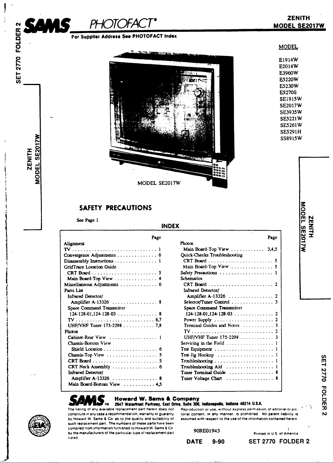
MODEL SE2017W
E1914W
E2014W
E3960W
E5220W
E5230W.
E5270S
SE1915W
SE2017W
SE3935W
SE5221W
SE5261W
SE5291H
SS8915W
:.
---.,:
"0 .•••
e
Alignment
lY 1
Convergence Adjustments . . . . . . . . . . . . . . ~
Disassembly Instructions . . . . . . . . . . . . . .. 1
GridTl1ICeLocatioo Guide
CRT Board . . . . . . . . . . . . . . . . . . . . . . . 5
Main Board-Top View 4
Miscellaneous Adjustments . . . . . . . . . . . . . 6
Pans List
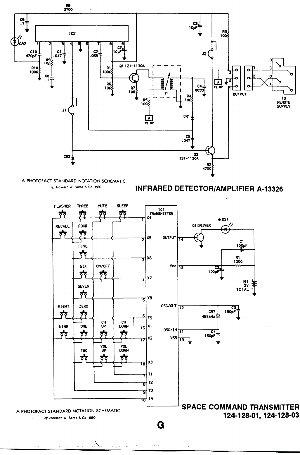
Infrared Detector!
Amplifier A·13326 8
Space Command Transmitter
124-128-01,124-128-03 8
lY 6,7
UHF/yHF Tuner 175-2298 7,8
Photos
Cabinet-Rear View .
Chassis-Botlom View
Shield Location . . . . . . . . . . . . . . . . . . . 6
Chassis-Top View ... . . . . . . . . . . . . . . . 5
CRT Board . . . . . . . . . . . . . . . . . . . . . . . 5
CRT Neck Assembly . . . . . . . . . . . . . . .. 6
Infrared Detector!
Amplifier A-13326 8
Main Board-Bottcm View 4,5
I!
.a.1!
~ rM
The hstlng of any
constllule In anycasearecommendallon, warranly or guaranty lonal contenl. ,n any manner, " prOhibited No patent lIablllly "
by Howard W. Sam.&Co. as 10 lhe Quallly and sullablllty 01 a.sumed with respeCllo Ihe use olthe Inlormallon contaIned herein .
···,······
•uch replace";en! part. The n~mbers ollhe.e parts have been
compIled Irom ,nlormallon furnIShed to Howard W Sam.&Co
by the manufacturers ot the parlocular Iype 01replacemenl part
listed
Howard
2647 Wlterfrolt Plrtway, East
available replacement
W.
Sam.&Company
part herein does not Reproduction or use. without express permls~uon, 01
Photos
Main Board-Top View 3,4,5
Quick-Cbecks Trooblesbooling
CRT Board . . . . . . . . . . . . . . . . . . . . . . . 5
Main Board-Top View 5
Safety Precautions .. . . . . . . . . . . . . . . . .. 1
Schematics
CRT Board . . . . . • . . . . . . . . . . . . . . . . . 2
Infrared Detector!
Amplifier A-13326 2
Selector/TUDerCartrol . . . . . . . . . . . . . . . 3
Space Command Transminer
124-128-01,124-128-03 2
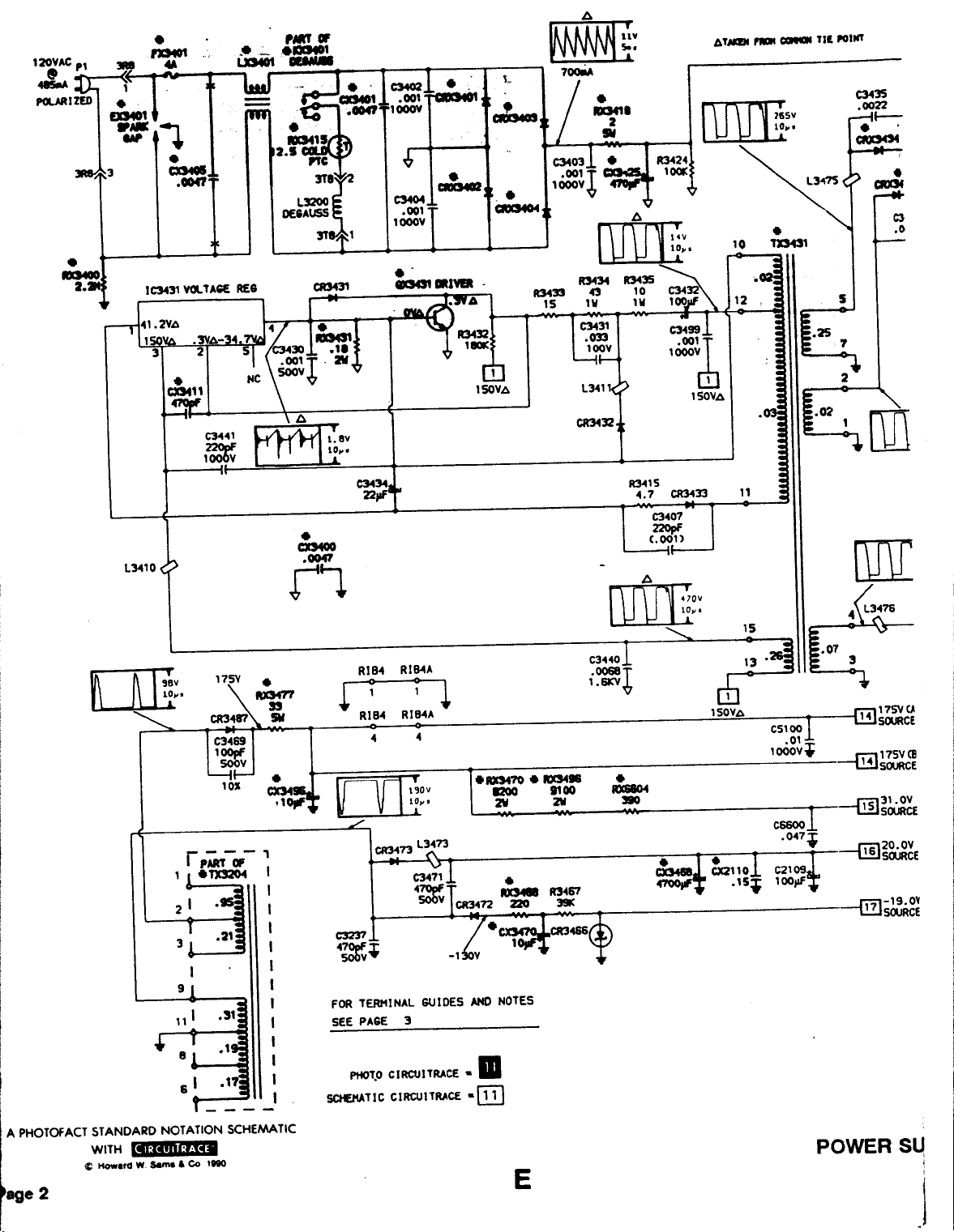
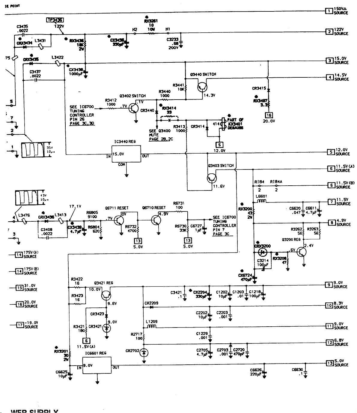
Power Supply .. . . . . . . . . . . . . . . . . . . . 2
Terminal Guides and Notes 3
lY 2
UHFfVHF Tuner 175-2298 3
Servicing in the Field . . . . . . . . . . . . . . . .. I
Test Equipmenl . . . . . . . . . . . . . . . . . . . .. 1
Test-Jig Hookup 1
Trooblesbooting . . . . . . . . . . . . . . . . . . . .. I
Trooblesbooting Aid 1
Tuner Terminal Guide 8
Tuner Voltage Chart 8
DrIYI,
Sultl 300,
IlId1InapoIII, IlId1Ina
41214 U.S.A.
ed,tor,al
or pIC-
Page 2
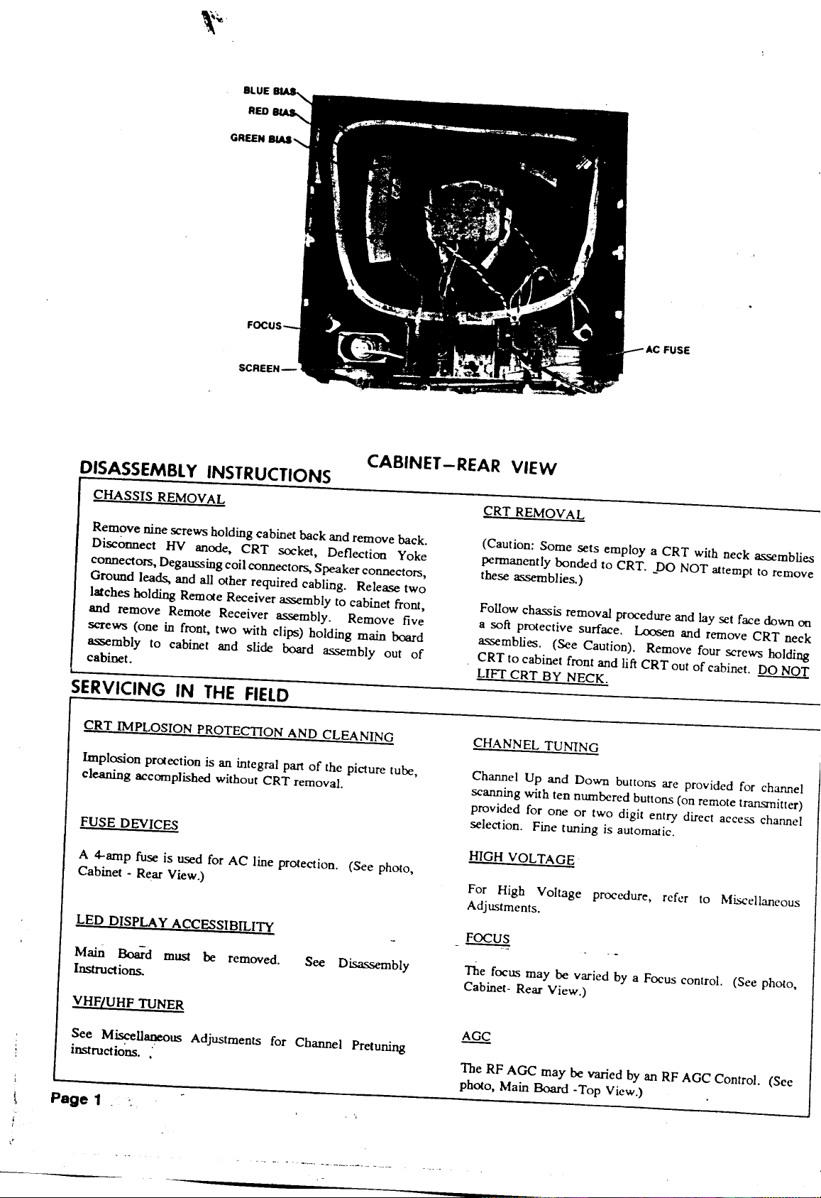
BLUE
REO
Remove nine screws holding cabinet back and remove back.
DiscOnnect HV anode, CRT socket, Deflection Yoke
connectors, Degaussingcoil connectors, Speaker connectors,
Ground leads, and all other required cabling. Release two
latches holding Remote Receiver assembly to cabinet front,
and remove Remote Receiver assembly. Remove five
screws (one in front, two with clips) holding main board
~mbly to cabinet and slide board assembly out of
cabinet.
Implosion protection is an integral part of the picture tube,
cleaning accomplished without CRT removal.
A 4-amp fuse is used for AC line protection. (See photo,
Cabinet - Rear View.)
Main
Boafd
must be removed.
Instruct ions.
(Caution: Some sets employ a CRT with neck assemblies
permanently bonded to CRT.
PO
NOT attempt to remove
these assemblies.)
Follow chassis removal procedure and lay set face down on
a soft protective surface. Loosen and remove CRT neck
assemblies. (See Caution). Remove four screws holding
CRT to cabinet front and lift CRT out of cabinet. DO NOT
LIFT CRT BY NECK.
Channel Up and Down bullons are provided for channel
scanning with ten numbered buttons (on remote transmiller)
provided for one or two digit entry direct access channel
selection. Fine tuning is automatic.
For High Voltage procedure, refer to Miscellaneous
Adjustments.
The focus may be varied by a Focus control. (See photo,
Cabinet- Rear View.)
See Miscellaneous Adjustments for Channel PretuDing
instruct ions. :
The RF AGC may be varied by an RF AGC Control. (See
photo, Main Board -Top View.)
Page 3
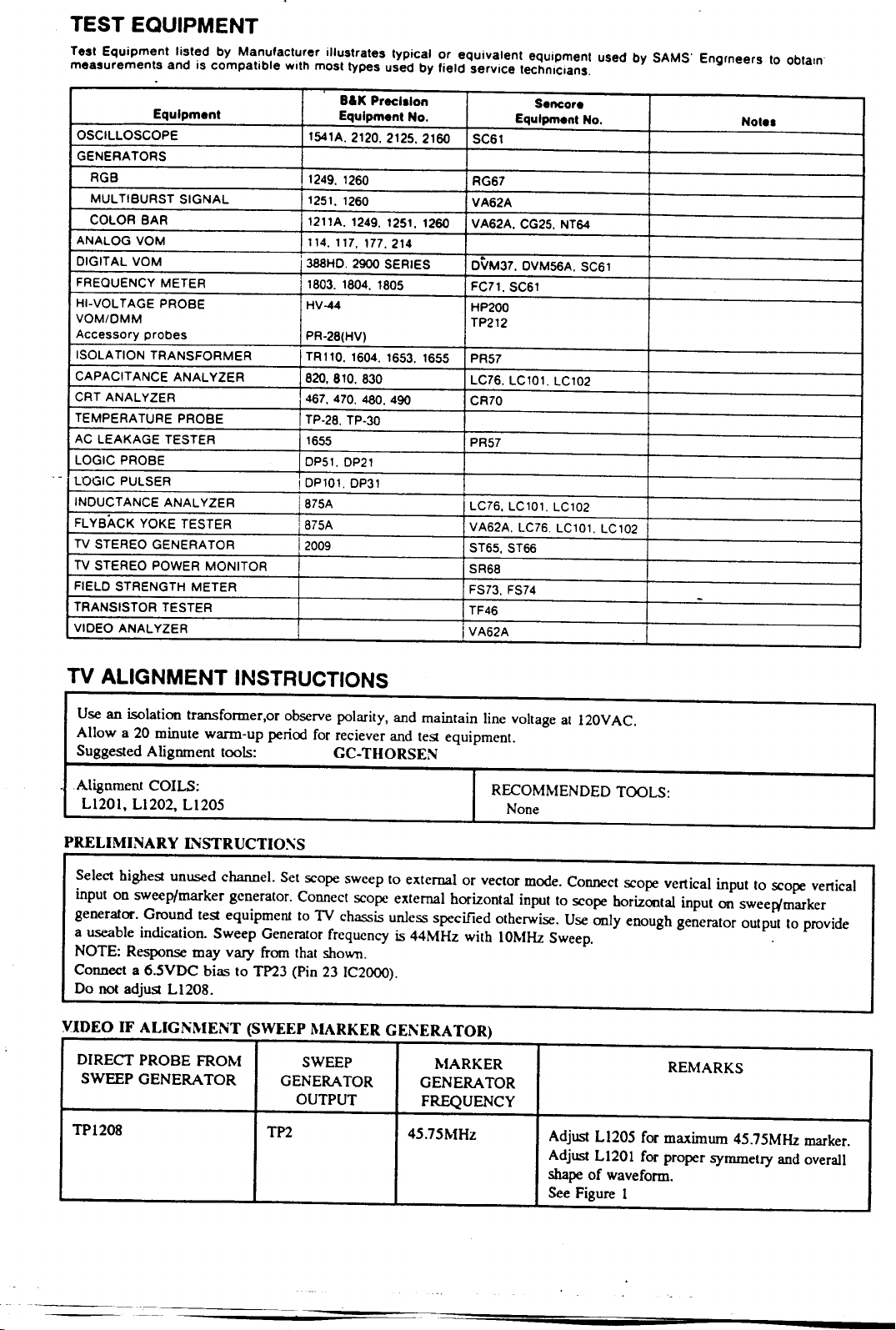
Test Equipment listed by Manufacturer illustrates typical or equivalent equipment used by SAMS' EngIneers to obtain
measurements and is compatible with most types used by field service technicians.
Equipment
OSCILLOSCOPE
GENERATORS
RGB
MUL T1BURST SIGNAL
COLOR BAR
ANALOG VOM
DIGITAL VOM
FREQUENCY METER
HI-VOL TAGE PROBE
VOM/DMM
Accessory probes
ISOLA TION TRANSFORMER
CAPACITANCE ANALYZER
CRT ANALYZER
TEMPERATURE PROBE
AC LEAKAGE TESTER
LOGIC PROBE
LOGIC PULSER
INDUCTANCE ANALYZER
FLYBACK YOKE TESTER
TV STEREO GENERA TOR
TV STEREO POWER MONITOR
FIELD STRENGTH METER
TRANSISTOR TESTER
VIDEO ANALYZER
BIK Precision
Equipment No.
t541A. 2120. 2125. 2160 SC61
1249. 1260
1251.1260
1211A. 1249.1251.1260
114. 117. 177. 214
388HD. 2900 SERIES DVM37. DVM56A. SC61
1803. 1804. 1805 FC71. SC61
HV-44
PR-28(HV)
TR110. 1604. 1653. 1655
820.810. 830
467.470. 480. 490
TP·28. TP-30
1655
DP51. DP21
I DP101. DP31
875A LC7S. LC10l. LC102
[875A
12009
RG67
VA62A
VA62A. CG25. NT64
HP200
TP212
PR57
LC76. LC101. LC102
CR70
PR57
VA62A. LC76. LC10l. LC102
ST65. ST66
SR68
FS73. FS74
TF46
VA62A
Senc:or.
Equipment No.
Note.
-
Use an isolation transformer,or observe polarity, and maintain line voltage at 120VAC.
Al10w a 20 minute wann-up period for reciever and test equipment.
Suggested Alignment tools:
GC-THORSEN
.Alignment COILS: RECOMMENDED TOOLS:
Ll20l, Ll202, Ll205 None
Select highest unused channel. Set scope sweep to external or vector mode. Connect scope vertical input to scope vertical
input on sweep/marker generator. Connect scope external horizontal input to scope horizontal input on swee(¥marker
generator. Ground test equipmern to TV chassis unless specified otherwise. Use only enough generator output to provide
a useable indication. Sweep Generator frequency is 44MHz with lOMHz Sweep.
NOTE: Response may vary from that shown.
Connect a 6.5VDC bias to TP23 (Pin 23 IC2000).
Do not adjust Ll208.
DIRECT PROBE FROM
SWEEP GENERATOR
TPl208 TP2
SWEEP
GENERATOR GENERATOR
OUTPUT
MARKER
FREQUENCY
45.75MHz
REMARKS
Adjust Ll205 for maximum 45.75MHz marker.
Adjust Ll20l for proper symmetry and overall
shape of waveform.
See Figure 1
Page 4
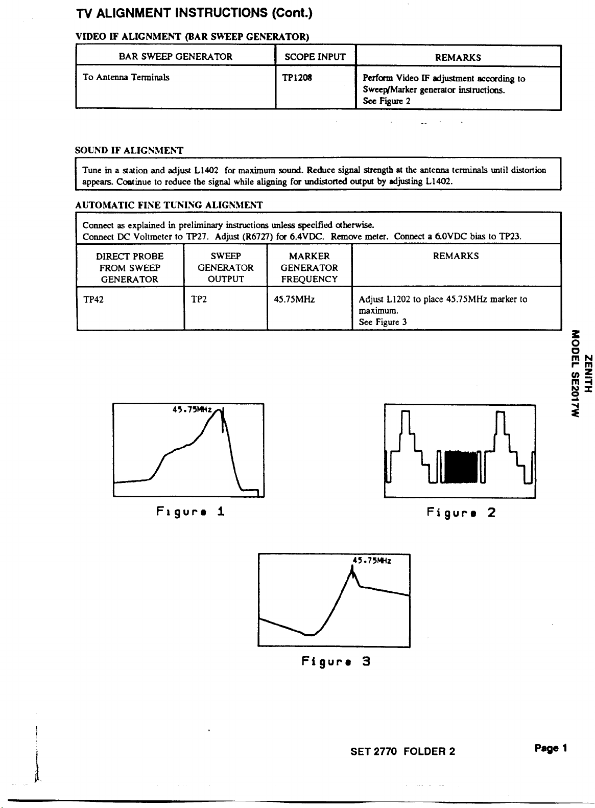
BAR SWEEP GENERATOR
SCOPE INPUT
REMARKS
To Antenna Terminals
Tune in a station and adjust L1402 for maximum sound. Reduce signal strength at the antenna terminals until distortion
appears. CODtinueto reduce the signal while aligning for undistorted outputbyadjusting L1402.
Connect as explained in preliminary instructions unless specified aherwise.
Connect DC Voltmeter to TP27. Adjust (R6727) for 6.4VDC. Remove meter. Connect a 6.0VDC bias to TP23.
DIRECT PROBE
FROM SWEEP
GENERATOR
TP42 TP2
SWEEP
GENERATOR
OUTPUT FREQUENCY
TP1208 Perform Video IF adjustment according to
Swee~Marker generator instructions.
See Figure 2
MARKER
GENERATOR
45.75MHz Adjust L1202 to place 45.75MHz marker to
maximum.
See Figure 3
REMARKS
Page 5
•
A'104OO
2.
•
~
3M ~
1
•
DI401
'="-.
•
ClIHlI
.0047
•
lDI301
.1'
2V
C3402
.001
l000v
C3404
.001
l000V
•
•
CIalHII
I
lSOVA
1.
c:,.
•
CIIDt04
1G433
A
f[ff[f]llV
7001iA
15 111 111
s••
•
10434 1G435
C3431
.033
L341
43
l00V
10
1G424
1001:
r---'
PlItT",
I .TX3204
~8V
~.
I
I
I
I
I
I
I
I
I
I
I
I
I
RIB4
RIB4A
o
1
~1
RIB4A
.Rll347O • D3418
1200
2V :N
•
U34II 10467
CA3472
FOR TERMINAL GUIDES AND NOTES
SEE PAGE :3
PHOT.O CIRCUlTRACE •
SCHEllATIC CIRCUITRACE •
II
[ill
Z20
1100
3!llC
CR3432
•
Rll6804
-
[II[
A PHOTOFACT STANDARD NOTATION SCHEMATIC
WITH
H'·Billi·f."'
c:
Howard W. Same&Co 1190
POWER S~
!
Page 6
------------------------------------------------m~
~ tb,
1 10
e
lllGUl
,.
2lI
•
CX343l1
l000Jlf
H2 1011 Ifl
C3233
,68T
2OOV·
SEE IC6700
TUNING
CONTROlLER
PIN 26
PAGE 3C,30
R3412
1000 .7V
113440 101C
1000
SEE 03400 1000
IlUTE
PAGE 2B,2C
Q6710RESET
4.
R3441
R3413
R6731
100
R6730
33lC
13
S.OV
C67Tl
lj1f
03403 S\lITCH
SEE IC6700 2l/
TltllN6
CONTROlLER
PIN 7
PAGE 3C
•
R)l32OO
43
CR3415
•
RX34I'1
3.
2O.0V
RIB4
2 2
L6601
•
16
RIB4A
R3262 R3263
Q32OORE6
56 56
S
6
6
12.0V
SOURCE
l1.SV(A)
SOURCE
".SVCB)
SOURCE
l1.SV
SOURCE
•
RX3201
C6625
10jlf
30
2W
6
11. SV(A)
1C6601 RE6
C2202
10""
C270S
4.7j1f
C6626
220""
C6630
.1~
Page 7
2
~3V
RSl00
100
.wwl
BAS 1000
2000
10•..•
CSl01
.001'
(.0022')
RS109
22
RSl1S
RS121
1500
RS103
1SIC
17SV~)
'"
H
lS100
f11Tl
I I
I
~lV
1tS'l0l
2200
I
£S1 00 SPAAII:
!6AP
to..,.
SEE TlC3201
PAGE 2
X
~V
~.
,
~5V
RS102
100
8l~AS
2000
~5V
RS'IOl
100
GREEN B AS
~
2000
to..,.
CSl03
.001'
(.0022>
10,...
C5102 RS110
.001'
(.0022>
RSll'
150
RSl11
RS117
RS123
QSl01
• 'TV
RS116
RS122
22
1000
1500
22
1000
1500
RS10S
liRE£N
RSl01
LSl02
1SIC
1"
H
17SVW
0t1T lS101
1SIC
1"
H
17SVW
f11Tl
•
I
f11Tl
I ,
I ,
~2V
I
•
17SVCA>
CS101 R5127
.01T 110f(
1 leV .••
10.,.
H
DAS TO CRT
FSHIElO
FOR TERHIN,4L iUlOES AND NOTES
SEE PAGE'
PtlO'TO CIRCUlTRACE •
SCttEI1ATlC CIRCUlTRACE •
CABLING.
HEAVY LINES REDUCE
USE Of MULTIPLE LINES
A PHOTOFACT STANDARD NOTATION SCHEMATIC
WITH
O,,-IYilli·f.Gi
©
Howard W Sam.&Co 1990
II
[ill
041
fA
CRT BOARD
SET 2770 FOLDER 2
Page 8
C10
470pF
R9
.0",,71
ISO
C8
C1
.068
C2
C3
10""
7
"1
A PHOTOFACT STANDARD NOTATION SCHEMATIC
©
Howard W Sams&Co 1990
IC1
TRAHSI1ITTER
X4
C5
.0",,71
Q2
121-1130A
.051
I
OUTPUT
II
TO
REI10TE
SUPPLY
C2
100""
81 '-
3V
-=-
TOTAL
-1
C4
lSOpF1
SPACE COMMAND TRANSMITIER
124-128-01, 124-128-03
Page 9

lOEO PROCESSOR
V 4. V J.7V
4 J2 R1404
Cl405
.22~
:.0681
--
IDYl YOIC!:~
I
I
I
7500
--
~v
~.
~V
~.
TAICDl IIITH
IIAIt SlI!fP lIOEltATOR
----
a-
-
,
51'1 L2201
4P4
162 6.9
PRESET
R2203
(470)
: R2206
22: lOOlC
: C2211 R2221
: .01.?SOO
: CR2204
I
I
I
I
-:-_1
700
750
,
I
I
1 -----.
R2294
PICTURE
101C
T
QJ400HUTE
R3401
22IC
RJ402 ~22
22IC
22jIF
(ll2lO
i---------------
, 24
,
I
R229S
I
I
COLOR
,
I
I
: 1SIC
I
I
I
I
I
I
: PART OF Ml (NON-REPAIRABLE)
101C
SQ::
C0804
l00jIF
PART
1C2000IF/VIOEO PROCESSOR
R2297
SHARP-
NESS
101C 8200
~
4P4l1
OF
S.JV
1
i-----------------i
I ,
: R2298 23:
I
__ : lEVEL
12K BRI6HTNESS
BLACK
SOO
1R22991
RA$E
SOOO
27
~---------------------------------------------------------------
10
B.2V
R222J
J900
C2219
1
C2220
R22169•
4700
I---
0V
JS3RJSJ
• I
CX32&1 :
2
.33; :
I
i----- .•~
CJ2571 RJ2S8
.Dr
101C
,------+
I
m
122V
TERMINAL GUIDES AND NOTES
PAGE 3
rlOTO CIRClJITRACE ••
1ATlC CIRCUITRACE •
[ill
SEE POWER
SUPPLY
PAGE 2E
SEE CRT X
FILAI1EHTS
MGE 2tl
SEE POWER
SUPPLY
PAGE 2E
.R324IA
FOCUS
•
11M!
HV ANODE
21.OKV TO
22.SK"i
•
RX3217
AJ A4
" "
•
RX3233
ZZO
,-.,.".,.,.--.
I I
, I
•
RlC3214
1
1
·CX3219
."
1X
S
12.0V
Page 10

R5124
RI B3 RI B3A (2200)
4?00
RIB3 RIB
2 2
R2216 9.0V
CIl2201 4700
i
R22t9 R2213
221J ]X
9
9
9.0V
CR2706
C2205
10pl'
R2212 C2214 1 • 1 39pF 2000
2.2" 1p1'
9
9.0V
L2301 C2303 R2304
14
17SVU)
C2304
.01.
rnn1'7ev
~.
11. SV(8)
~.v
TAaII 1I1T1l UII
MIP IUCAATQIt
6
10•.••
R2210 C2231
270
1 RIB3 RIB3A
C2209
270pF.
CR2207
3 3
4
R6704 R6703 C6704
3000 15K .001.
13
5.0V
SEE lC6700
TUNING CONTROLLER
PIN 12
PAg 3C
R2719
2000
r
RIB3
0 0
4
RIB3A
4
1
Page 11

CI223
1I.2pf
*.2SpF
RI23ll
5100
C68OO)
r -
I
TAICDl III TIt lWt
~5V
~.
PAg 3C
ITPl208J
SEE Q6l101
VOLlH:
PART Of'
1C2000 I' /'VID(O NDCUSOII
1 7V
1 R'
Rl407 Cl40S
510
.22.
C • ...,
~
RI236
1000
RIm! CI224
39lC~ .01.
,
m
9.0V
R2114
VERT
SIZE
201:
R2118
1 SIC
CI8K)
14
17SV CB)
C1201
.01 .•
R2101
2700 10.2V
R2103
•
CX2111
47O-,F
• Rll2118
33K
2.4
C1219
.01 .•
C2108
.01
lOll
C2105
.22.•
:~
1
CX3261
I
I
I
:
[
3S3"cf
.'
.33.•
,
c~J.
.33T
'--
F
R2715
3300
C27071 R32SS
.0000T 1100
I
••
6
11.SVCA)
6
11. SV (A)
C3202
470pF
SOOV
lOX
FOR TERMINAL 6UH
SEE P"GE ,
PHOTO CIRCUITR,\
SCHEMATIC CIRCUITR}
Page 12

n.SY
SEE IC6700
TUNING CONTROlLER
PIN 13
~
•
• 1230
11
9.0V
el227
.001. 58
1
5.1
RlC1211
C670S
.47";
RI238
1000
R12231 Cl224
39K~ .01.
I
m
9.0V
ffln73V
~.
•
RllS224
15
R2704 R270S CR2101
C27f12 C271S
~I1SOpf•.
R2714
100
PART Of
1C2000IF/vIDEO PROCESSOR
4.9V 4.6V OV
61 63 1
2200 430 SO
0012*
KHz
o
R2703
1000
C2708
4.1";
~V
LLLU..:i1
R2114
VERT
SIZE
20/(
R2118
15K
C18K)
R271S
3300
C27071 R325S
.0000T 1100
I
••
CABLING.
HEAVY LINES REDUCE
USE OF MULTIPLE LINES
A1 A2
ACT STANDARD NOTATION SCHEMATIC A -,---,------------------ _
WITH
Hi·Ailli,'·D-
© Howard W Sama
&
Co 19l1O
Page 13

.--------------------------------.--------------------------_
: ~ ~ " ~ ~ $
: OMICf'f
:
I
•
,
I
I
•
,
,
I
,
,
,
I
-'- -'- -'- -'- -'- -'-
58
All
Qt.
-'-
510
IWI)
-'-
,10 16 lB 12 14
L__
R6715 1000 1000 1000
1000
R6721
Qt •
511
10Ft
CM.• VCI..• VCI...• All
-'-
---------- ---------
R6720
C"BllNG.
HE"VY LINES REDUCE
USE OF MULTIPLE LINES
--------_.
R6719
13 19 15
----------
R6718
1000
SEE TUNER
=LER J67~OO L6700 ~~~7
PAGE 3B
REtIOTE CONTROL
15 NOT USED
IN ALL 11ODEL5
SEE RE/1OTE
PREAMP
PIN 1
PAGE 26
SEE REI10TE
PREAW
PIN 2
PAGE 26
SEE REI10TE
PR£Nt>
PIN 3
PAGE 26
...
-----
...
Qt ••
59
ADO
-'-
-----------
R6716 R6717
1000 1000
R6'709
4700
C870B
IOpf.
llllB
~
1
~
12.0V
-------------
R6'744
3300
R6743
3300
I
I
•
--------_.
C
,
C8711
,001.
C8710
,001•
C8712
.001.
C8713
.001.
C6714
,001.
C8715
.001.
C8709
.001.
R6799
1500 CR6700
C8702
91pf.
L6701
SEE Q6710
RESET
PAGE 2F
SEE Q'Z702
VERT SYNC
PAGE 20
SEE 1C2000
IFIVIOEO
PROCfSSOR
PIN 42
PAg 2A
R67'37
91
R6'738
91
R6739
91
R6740
91
R6741
91
.Jl6735
91
C8701
2Opf .•
IC6700
"' ••••• CONTROllER
'Z7 4.8V
2tl 4.8V
.8V
19
21 4.9V
23 2.BV
8V
242•
25 4.9V
.BY
lB
g1.6V
10 1. 4Y
161.SV
B 5.0V
22
9V
74•
0V
6
12 .BV
.2V
1.7V 15
OV 4
OV
1. 6V 14
"R67OB
4700
SEE 03402
SVITQl
PAg 2f,iI'
13
5.0V
13
5.0VB4.9Y
5.0V 4.9Y
Q67ooVCl..lIE
13 B
R6713
2000
.
~
7
l1.SV
Q6704 LED SIIITCM
~.
4.6V (C67201
I~ .•
m
4.9V
A PHOTOfACT STANDARD NOTATION SCHEMATIC
WITH
ltIi'·Ailli·e.'3'
'" Howard W Sama • Co 1990
Page 14

Q&7OOVOlllE
.
Q6701LEO SWITCH
8
1.9V
~
I1.SV
.0
R6605 Rli602 C6602 R6603
100 1. .01 _
R6600 C8601 C6&05 RS711
_ .047 •• 017. 100
15
31.0V
C6608
10pF
0S601 !iU'ER
SEE 1C2000
IFIVIDEO
PROCESSOR
PIN 30
PAGE 29
7
FOR TERMINAL GUIDES ANa NOTES
SEE PAGE 3
R6607 II.SV
1700
7
II.SV
7
IWCl
SWITCH 10pF
C&607
r
I1.SV
~
S.OV
SEE lUER
IH' TUoIIN$
VOlTA'f
PASE
P
SEE lUER
Vtf' Tlill N6
VOlTA'f
PASE 3A.3B
SEE TI.t€R
Vtf' 8+
+12V
PAGE
3A
SEE lUER
IH' 8+
+12V
PASE 38
SEE TUNER
SU'ER 8AND
SWITCH
PAg 3A.3B
SEE TUNER
Vtf' BAND
SWITCH
PAGE 3A
SEE TUNER
"
+12V
7 PAGE 3B
PRESCALER
13 pAGE 3D
SEE TUNER
8+ +SV
IXER
8+
PHOTO CIRCUITRACE •
SCHEtIATlC CIRCUlTRACE • [D]
81 B2 83 B1 as B6 B7 Be B9 810811 812813811 B15 816
lUll
a
81 813 B6 815 Be B9 B7 816 as 811 83 81281 810 B2 all
B
C7
I
c
Page 15

A
F
II ~
Xl
1"
C3
8.¥
L2~
102 Cl0l ::
¥
.001
~
103 L101 ~
:r
t
rrn
m lJfPFl
~
---
-
lJ
Ll02~
Ll03~
C9
26pF
cs
410pF
Cl 470pF 410pF
22pF
CR2
¥
R6
2700
~ ~
L4
~
r
¥
~t
CRI
L3~
CS
lic?PF
1¥
2700
R2
2700
A3
~
Rl01
2700
lloo
-
iim
R4
39K
Jl
U
~
I"
Rl02
2700
~
Ll04
CIOS CRl0l
4pF
C1(l~:;:
.001
Rl03
1200 1000
Rloo
C1S1
:oin
Cl52 Cl53
I
,
~l
UtF
Rll0
1000
AGe
Ll07
~
CRl02
Rl04
39K
~C¥
•
r--
001
L6
,;.;.
1
Vtf'
T
CRl0~
Cl08
l20pF
I
C12
C~~
4.7
"
JIll
L7~
L.:"
RIOS lOOlC
S6IC
~
~
~
Rl20
Cl54
I
.001
I
vtf'
~
~
Cl~:
410pF
C14
410pF
J2
Rl06
Rl07
lOOlC
Vtf'
Rf N'P
Q3
"
Ln-,
100
R24
S600
UtF
Ql
R7
1000 10lC
Rl08
1500
SC113
~.001
~
~
Rf ~
220
R11
-
~
R8
~
Rl09
270
R12
1000
R9
1.
Cll1
.~1
Cl'Qg
.~1
Rl14
22IC
C17
-
Cl0
.OOl!
J3
L9
I
-
L109I1~
L1~8
V
Rl12
1200
R113
1200
Lll
....---
RIll
•
i
C23
L112~
1117 ~
Rl17
1200
Jl0
I
I
I
Q1
I
I
W
Ll
Ll
I
1;1
.C
C21 C22
:JOpf
CHI
~
'.:::::7
RIO
15K
CIS
470pFI
10
Cl14
.O~!1
Rl1S
2700
Rl16
22IC
24pf'
ITh
~
•
Rl22
1500
Cl!~.
.001
Cll?
.001
RIS
15K
C116
.001
R20
1000
(
rnTI
CRl06
~104
C121
Cll~:
.001
R13
4700
1111 ~
CRl0S Ll14
.001
CR5
3pF
~~ I
vtf'
CT STANDARD NOT A TION SCHEMA TIC
~ Howard W. Sama&Co 19110
Page 16

C22
24pf
R15
151(
CIlS
m-.
'-"
C23
.001
I
l12
l13 C23
3!Ipf 20pf
111ll£R
DIODE
..
CR7
""'
l14 ~
R14
22K
C24
r
C20 2.7pf
.1¥
..
C'Z1
C2lI
l19
I
III
C33
2~¥
RIg
101C
I
~
~
R21
3000
C3~:
470pf
lH' OSC
Q2
w\ ~:
~ .Spf
-,g
C40
4pf
R23
511
I
,
C4~:
.022
112
R27
10lC
L21 (,
]3
l22~
R20 C30
1000
47Ft
..
~
R16
3000
L16 1000
rnTI
-
C116
.001
.
:
R124
1200
RID
!
I
I
(~'04
f
7
11 '148
Ll12~
LI14 Ll16
rnTl
CRl06 CRl07
C121
3pF
1117 ~ L118 ~
R117
1200
Cll~:
.001
Jl0
C~
I
I
I
vtf'
T\JlIN6
VOlTAGE
1800 Rl26
Ll13 ~
R118 .001 Rl30
'200
1
;0:,;
CRl08
rn1"l
Cl29
.001
Cl22
47pj
R119 3900 RI39
22IC
I
.
•
CRIll
1200 .001
Lll0§
,
(
~'09
C124
1t17.
R18
• Cl28
47pf
C;;
Cl~:
12Opl'
L119 ~
R121
5600
CRl10
C29
.~1
75
Cl30
.001
RI29
2000
C131
2.7pf
R131 CR112
2700
Cl~:~
62pF
RI28
1200
Rl32
1200
Jl04
RI27
5600
/JJ\
~
U
Cl~:
l.Spf
Cl~:
~~
R22
510
R28
20lC
Rl33
l2IC
vtf' OSC ~¥
Q6 1
CR113
L122§
4300
,
~
r;;
.~
C142
.001
~
Rl31
39IC
Cl~:
.001
Cl38
.022
CI37
.~1
H
C143
.~1
1126
-
;:;;m
Q4vtf' I1IXER
R141
2000
4 3 2
ICI PRESCAlER
r
5
~
CR114
L124 ~
C144
6pF
\6
foIC
R142
1127 C~:
rrin
220
!
~
C43
!!
.000I
Rl37
noo
R143
470
RI36
C~;::~
Ll2S~
CI39
4pf
511
Ll28~
Cl58
.2Di:.
IF AM'
(~
,47pf
I
as
R144
10lC
C1
.C
~
R"
Sf
Page 17

~
"'-=-',
-
470pf
_7~
470pf
n
'--
Rl06
os lOOK
6t
C13
C14
R24
S800
lH' RF
Ql
220
~
Rll
R7
1000 lC1C
Rl08
1500
R8
Lll
L9
C18
~
loW
¥
R12
1000
C17
470pF
~ J3 4700
R9
,.
I
Cl0
001
•
1
C21
3Opf'
CR4
.1i:\
~
RIO
R13
15K 15K
•••
CIS C116
47Opf1
Lll1 ~
C22
24pf:
RIS
.001
L12
C23
.001
C24
CRS
fJJ\
x;..' x;..'
C20
.1¥
R20
1000
C30
4iiF
L13 C23
CR7
UtI'
"IllER
DIODE
r
rnn rnn
3000
L17
R16
39pf
L14~
R14
22K
-
CRll1
at
20pf
C2lI
2.7pf
L16
L19
CR6
rm
R17
1000
R18
••• C128
47pf
LIe
,:
•
-
CD
2.¥
1
RIg
lC1C
C29
.0:9
7S
Cl30
.001
..
'
r---
~
RI29
2000
R131
ell
2700
Cl36
62pf
RI28
1200
C112
~
RI20
100
.
.
RIO?
lOOK
VIf'
Rf ""'
Q3
~
~,
~-,
5
-
C113
.001
Rl09
270
Cll1
.~1
ClOt
.~1
R1l4
22K
..
R124
Rl23
1200
R118
'200
1
101:1ti
.001
I
5U'fR
1800
L116
rrm
.
\
CRlce
C~;';
Cl29
.001
R119
22K
C124
.001
Rl26
1200
Lll0~
~
~'09
Rl30
3900
Rl32
1200
,
Cl26
3t'!'
Cl27
l20pf
L119~
R121
S600
CRll0
Rl22
1500
L109II~
L~8
F
RIll
10
RllS
R1l2
1200 47
R113
1200
2700
C114
.0:9
R116
22K
..
'
CRIOS
Cl~~ •
.001
Cll~ :
.001
(
L112~ L113~
Ll14
nrn
CRl06 CRl07
~
C121
3pF
C119
.001
~~ I
vtt'
L117~ L118~
R117
1200
Jl0
I
~'04
Jl04 (
R12'l
5&OC
,
Page 18

I
L1.
R21
01
47llpF
R26
750
1/4'1
R28
20lC
Cl'30
,001
Rl33
l2IC
r
Rl29 Ytf' OSC Cl33 J6
2000
R131
2700
C136
62pF
R128 L125
1200 CR114
Jl04
R132
1200 .001
Q6
L122
Rl,..
-
1
CI38
.022
C137
C143 R142 C147
.001 220 .001
L124
Rl37
3300
L26
L23
L24
JS
J4
R130
3900
Rl27
S600
R139
4300
CIS?
1
"I
+12V
leER
B+
L126
Q4 vtf' "I
R141
2000
leER
C144
6pF
L127
R143
470
1
6pF
L128
Clse
l
IF
CUlM
If AW
as
1:148
47
I
R144
10K
p1'
R146
S600
"'04 "'OS
C1S9
.001
I
\H'
B+ 8+
+12V
C1SO
001
•
1 ~
f"RESCALER
+5V
Page 19

TEST JIG HOOKUP
FUNCTION
CRT
YOKE
YOKE SEl1lNG
Check the AC Fuse (FX3401). If Fuse FX3401 is open,
check Bridge Rectifier Diodes (CRX3401 thru CRX3404),
Capacitors C3402. C3403, C3404 and C3405, Electrolytic
C3425. Apply 120V AC and check for 150V* at the
cathode of Diode CRX3403. If this voltage is missing,
check Line Filter (LX3401). If 150V* is presem, press the
Power Switch and check for 122V at TP3436. If 122V is
missing at TP3436, check the voltages and components
associated with the Voltage Regulator IC (lC3431), Driver
Transistor (Q3431) and the Horizontal Output Transistor
(QX320S). If the proper voltage is present at TP3436 refer
to the -Horizomal" section of this Troubleshooting guide.
Chek-A-Color
ADAPTER
B239
04141 PLUGI2AJ
FOCUS TAP
NO.
YPJ
P.C. BOARD
PLUG' 3S3
PINS 1,2
PINS 3,4
PIN 1 YELLOW
PIN 2 GREEN
If there is no video at TPI20S, apply AGC bias to pin 23
of the IF/Video Processor IC (lC2000). If video is now
present at TP120S, check the voltages, waveforms and
componems associated with pins 18 thru 27,29,37 thru 47
of IC2000, SWIF Driver Transistor (QI202) and the Video
Amp Transistor (Ql208). A defective AGC circuit can
cause an overloaded picture, excessive snow or loss of
audio and video. See the AGC Voltage Chart for AGC
voltages with signal.
BLUE
RED
AGC VOLTAGE CHART
IC2000
Pin 18 2.8V
Pin 23 5.7V
Pin 46 4.2V
Determine if TV is in shutdown, refer to the "High Voltage
Shutdown" section of this Troubleshooting guide. If TV is
not in shutdown, inject a horizontal signal at the base of the
Horizontal Output Transistor (QX3208). If horizontal
deflection is now present, check the voltages, waveforms
and componems associated with pins 60 thru 64 of the
IFfVideo Processor IC (lC2000), Horizontal Amp Tran-
sistors (Q3201, Q3202) and the Horizontal Driver Transistor
(Q3206). If there is still no horizontal sweep, check the
voltages, waveforms and componems associated with
(QX320S) and Transformer (TX3204). Check the voltages
and components associated with Diodes (CR3472, CR3473,
CR34S7) for defects. The high voltage rectifier is part of
Transformer TX3204 and if defective, will affect the
perf<X1D8OCeof the horizontal circuits. If the horizontal
oscillator is off frequency, check the voltages, waveforms
and components associated with pins 61, 62 and 63 of
IC2000. Horizontal linearity or foldover problems may be
caused by Capacitors CX322S and CX3229 being defective.
Inject a video IF signal at the IF input and check for video
on the CRT. If there is no video on the CRT, check for a
video waveform at TP1208. If video is present at TPl20S,
refer to the ·Video· section of this Troubleshooting guide.
Inject a video signal at TP1208 and check for video on the
CRT. If video is present, refer to the "IF-AGC" section of
this Troubleshooting guide. If there is no video on the
CRT, check for a video waveform at pin 53 of IC2000,
check the voltages, waveforms and components associated
with the Video Amp Transistor (QI203) and pin 53 of
IC2000. If video is present at pin 53, check for a video
waveform at TP5104. If the waveform is missing, check
the voltages, waveforms and components associated with
pins S, 13 thru 17,51,52,53 and Video Amp Transistor
Q5104. If the waveform is present at TP5104, check the
voltages, waveforms and components associated with the
Red, Blue and Green Output Transistors (Q5101, Q5102).
If the brightness is inadequate or cannot be controlled,
check the voltages, waveforms and components associated
with pins 14 and 15 of IC2000.
Check for a chroma waveform at pin 49 of the IF/Video
Processor IC (lC2000). If the waveform is missing, check
the components associated with pin 49. If a chroma
waveform is present at pin 49 of IC2000, check for the
proper waveforms at pins 9, 10, 11 of IC2000. If these
waveforms are missing, check the voltages, waveforms and
components associated with pins 2 thru 7, 9, 10, 11, 12 of
IC2000. Check the 3.5SMHz oscillator at pins 4 and 6 of
Page 20

IC2000. Check the voltages and components associaled
with the color control and pin 3 of IC2000. If thcre is
inadequate tint range, check the voltages. wavefonns and
components associated with the tint control and pin 2 of
IC2000. If the proper wavefonns are present at pins 9,
10,11 of IC2000, refer to the wRaster" section of this
Troubleshooting guide.
Inject a vertical drive signal at pin 54 of the IF/Video
Processor IC (lC2000). If vertical deflection is now
present, check voltages, waveforms and components
associated with pins 54, 55, 56 of IC2000. If there is still
no vertical deflection. check the voltages, wavefonns and
components associated with the Vertical Output IC
(IC2101). Yerticallinearity or foldover problems may be
caused by vertical feedback and bias circuits, check Electro-
lytics C2101, C2102, CX2107, CX2111 and C2112 forde-
fects.
Select an active TV channel and check for an audio
waveform aI pin 28 of the IF/Yideo Processor IC (IC2000).
If there is no audio, check the voltages, wavefonns and
components associated with pins 28, 30 thru 36 of IC2000.
If audio is present at pin 28, check for audio at pin 4 of the
Audio Output IC (IC0810). If audio is missing, check the
voltages, wavefonns and components associaled with
IC0801. Check pin 30 of IC2000 for 1.2V at mute and
5.0V at Maximum volume.
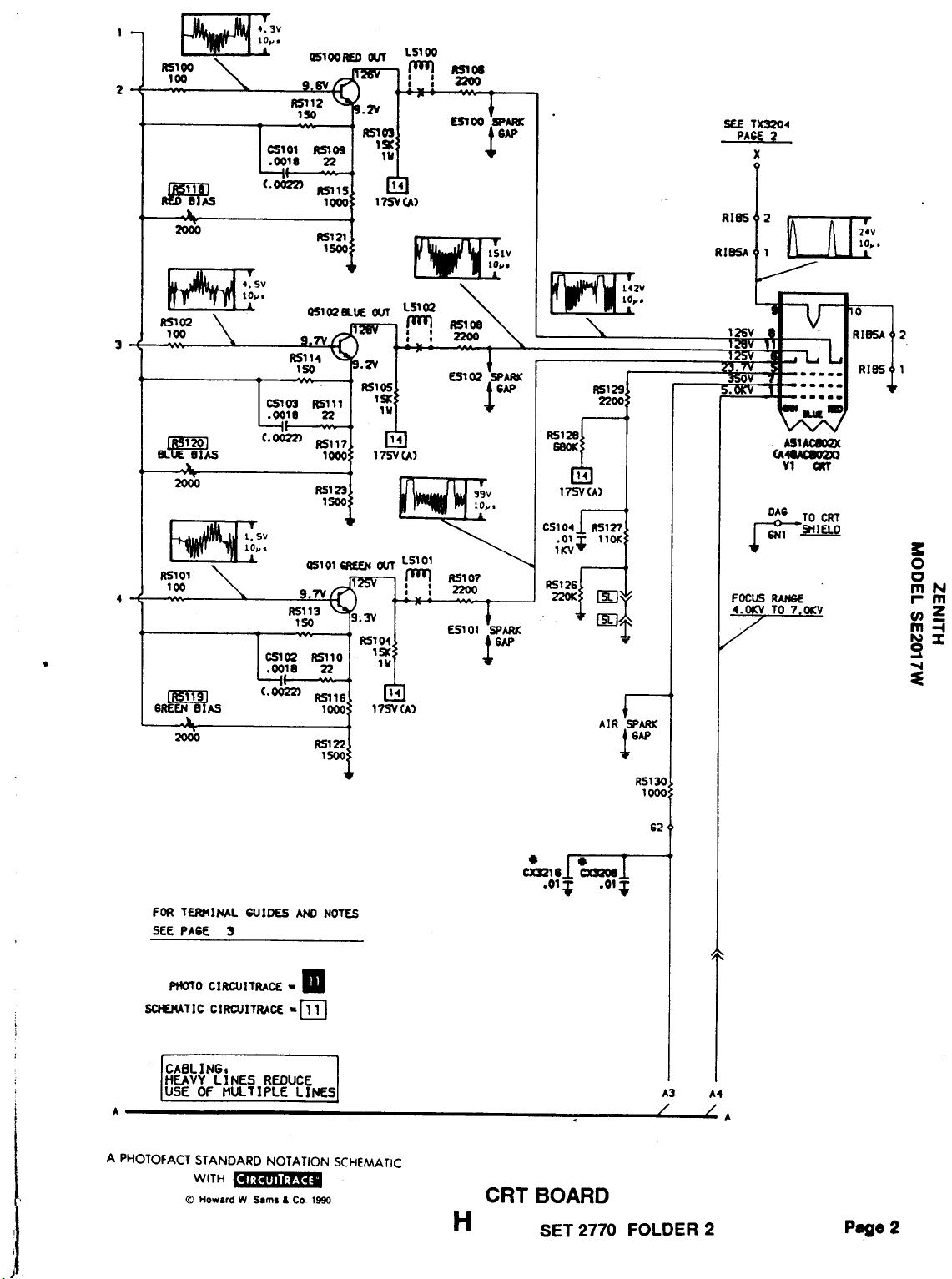
(Q5100). If there is no green, check the voltages and
components associated with pin 10 of IC2000, and Green
Output Transistor (Q5101). If there is no blue, check the
voltages and components associated with pin 11of IC2000,
and Blue Output Transistor (Q5102). If the raster has a
keystone shape, check the Deflection Yoke (DYl). If the
raster has height or width problems, refer to the WYerticalw,
wHorizontalWand wPower"sectioos of this Troubleshooting
guide.
The high voltage is monitored by DiodeCR3206, rectifying
pulses from the Horizontal Output Transformer (TX3204).
Should the high voltage increase, the rectified voltage at the
base of the Shutdown Transistor (Q3299) will also increase
and trigger the shutdown circuit at pin 1 of IF/Video
Processor IC (lC2000). To troubleshoot, remove Diode
CR3206 from the circuit and use a variac for AC power.
Start at 90Y AC and increase as necC$U)' to locate the
defect. Return CR3206 to the circuit.
NOTE: Care should be taken in defeating the high voltage
shutdown circuit, as this may cause excessive X-radiation
and damage to the CRT, Transformer TX3204 and
associated components. Monitor the high voltage and
troubleshoot.
Voltages Taken with TV in Shutdown
IC2000
Pin 1 l.5V
TP3436 134V
If there is no vertical or horizontal sync, check the voltages,
wavefonns and components associated with pin 57 of the
IF/yideo Processor IC (lC2000). If there is no vertical
sync, check the voltages, waveforms and components
associated with pins 54, 55 and 57 of IC2000. If there is
no horizontal sync, check the voltages and components
associated with pins 57 and 64 of IC2000.
Check the CRT and CRT voltages. If there is no red, check
the voltages and components associated with pin 9 of the
IF/Yideo Processor IC (IC2000) and Red Output Transistor
Apply 120V AC, turn set On, set a1lcustomer controls for
normal operation and apply a 16.0V bias through an
isolation diode to the base of the Shutdown Transistor
(Q3299). If set docs not lose raster and sound the
shutdown circuit should be repaired To resume normal
operation, remove AC power and wait 30 seconds then turn
set On.
Page 21

SEMICONDUCTORS (Select reolacement for best results)
ITEM
No.
CR2101
CR2101 103-279-12A
CR2201,2,3,4
CR2205,6. 7 ..
CR2208
CR2209
CR2301
CR2702
CR2703
CR2704
CR2705,6 103-398
CR3206
CR3257
CR3414,15
CR3421
CR3422,23
CR3431,32,33
CR3440
CR3466
CR3472 103-284A
CR3473
CR3487
CR6702,3
CR6711
CRX3200
CRX3207
CRX3401 THRU
CRX3404
CRX3434
CRX3435
CRX3436
IC0801
IC2000
IC2101
IC3431
IC3440
IC6600
IC6601
IC6700
Q1202
Q1203
Q1203
Q2101
Q2701
Q2701
Q3200 121-966-03
MFGR.
PART No.1
TYPE No.
103-254-01
103-398
103-429
103-142-01
103-330A
103-398
103-279-14A
103-398
103-279-10A
103-326A
103-254-01
103-3~18A
103-398
103-344A
103-254-01
103-399-29
103-326A
103-398
103-398
103-279-08A
103-409A
103-315-06A
221-422-01
221-467
221-468
223-28
221-213-4
221-419
221-166
221-493
121-1158A
121-895A
121-986A
121-975A
121-895A
121-986A
NTE ECG
PART No.
NTE116 ECG1l6
NTEI77
NTE116 ECGl16
NTES014A ECG5014A
NTESOI0A ECG5010A
NTES52 ECG552
NTE116 ECG116
NTES018A ECG5018A
NTE116
NTE116 ECG1l6
NTES52
NTES52
NTESOO8A
NTES021 A ECG5021A
NTE116 ECG116
NTE1374
NTE1790 ECGI790
NTE123AP ECG123AP
NTE159 ECG159
NTE123AP ECGl23AP
NTE123AP ECGl23AP
NTE159
NTE152 ECG152
PART No.
ECGI77
ECGl16
ECG552
ECG552
ECG5008A
ECG1374
ECG159
TCE
PART No.
SK3313/116
SK9091/177
SK3312
SK6A8/5014A
SK5Al/5010A
SK9000/552
SK3313/l16
SK9Al/5018A
SK3313/116
SK3313/116
SK9000/552
SK9000/552
SK4A3/5008A
SK12A/5021A II
SK3313/116
SK3853/l374
SK9850
SK3854/ 123AP
SK3466I159
SK3854/l23AP
SK3854/123AP
SK3466/159
SK3893/152
N4
II
II
II
II
II
Page 22

PARTS LIST AND DESCRIPTION (Continued)
When ordering parts, slale Model, ParI Number, and Description
SEMICONDUCTORS (Select replacement for best results)
ITEM
No.
Q3201,2 121·97SA
Q3206
Q3299 121·973A
Q3400 121·97SA
Q3402
Q3403 121-1102A
Q3421
Q3440 121-1102A
QS100
llIRU
QSI02
QSI03
QSI04
Q66OO,l 121-1133A
Q6700,4.7 121-1133A
Q6710,l1
Q6801 121-11JOA
QX3208
QX3431
MFGR.
PART
TYPE
121-1037
121·1040-01A
121-966-03
121-1140A NTE399 ECG399
12l-1019A
121-89SA
121-11JOA
121-1141-O1
121-1040-01A
No.1
No.
NTE
PART
No.
NTE123AP ECGl23AP
NTEl71 ECGl71
NTE1S9 ECGlS9
NTE123AP ECGl23AP
NTE123AP ECGI 23AP
NTE290A
NTE1S2
NTE290A
NTE1S9 ECGlS9
NTEl23AP ECGl23AP
NTE2302 ECG2302
NTE123AP
KG
PART
No.
ECG290A
ECGlS2
ECG290A
ECGl23AP
TeE NOTES
PART
No.
SK38S4/ I23AP
SK320l/17I
SK3466ilS9
SK38S4/123AP
SK38S4/123AP
SK3114N290A
SK3893/1S2
SK3114N290A
SK93S2I399
SK3466ilS9
SK38S4/123AP
SK9422
SK38S4/123AP
1#
-
II
Page 23

PARTS LIST AND DESCRIPTION (Continued)
·
ITEM
No.
CX0803
CX0806
CX2107
CX2111
CX2204
CX3204
CX3219
CX3405
RATING
470 25V 20% 22-7860-12
220 16V 20%
100 35V 20%
22-7859-10
22-7861-09
470 25V 20% 22-7860-12
330 25V 20% 22-7860-11
100 20V 35%
68 25V 20%
33 25V 20%
.004720%
22-7861-09
22-7860-27A
22-7860-C17A
22-7431-06
MFGR.
PART No.
ITEM
No.
CX3425
CX3436
CX3438
CX3439
CX3468
CX3470
CX3496
CX6724
RATING
470200V 20%
330 200V 20%
1000 25V 20%
4.7 35V 20%
4700 25V 20%
10 200V 20%
10 315V
470 10V 20%
MFGR.
PART No.
22-7819-10
22-7908-018
22-7860-13
22-8135A
22-7860-16
22-7962-11
22-7999-018
22-7858-12
ITEM MFGR
No.
C1223
C1226
CI403
CX2110
CX3206
CX3208
CX3216
CX3222
CX3228
CX3229
RATING PART No.
8.2pF 50V ±.5pF
22-7985-27
30pF NPO 50V 5% 22-8033-23
4.7pF 50Y ±.25pF 22-7985-19
.1550V 10% 22-8049-26A
--.012KY 20%
.1 50V 5%
.01 2KY 20%
530pF 3KY 10%
530pF 3KY 10%
22-7523-018
22-8048-24A
22-7523-018
22-8063
22-8063
.0056 1.6KY 3% 22-7672-40
ITEM
No.
RATING
CX3261 .33 250V 5%
CX3400 .004720%
CX3401
CX3405
CX3410
CX3411
.004720%
.004720%
-- .001 20%
470pF lKY 10% 22-7811-0IA
.001 lKY 10% 22-7811A
530pF 3KV 10% 22-8063
CX3412
.001 500Y 10%
CX3433 .0047 1.6KY 5%
MFGR
PART No.
22-7876-18
22-7431-06
22-7431-06
22-7431-06
22-7431-04 .
22-7786C
22-7672-16
Page 24

Page7
PARTS LIST AND DESCRIPTION (Continued)
When ordering parts, state Model, Part Number, and Description
COILS (RF-IF)
ITEM
No.
L1201
L1202 AFC
L1203
L1205
L1206
L1207
L1208
L1209
L1210
L1402
L2203
L2301
L2303
FUNCTION PART No.
Peaking
RF Choke
Picture IF
Peaking (.38uH)
Peaking (.38uH) 20-3858-01
Output IF
RF Choke
RF Choke .(27uH)
Sound IF Detector
RF Choke (120uH)
Peaking (47uH) 20-3907-20A
RF Choke (5.6uH)
(8.2uH)
MFGR
20-4172-02A
20-4172-12A
20-3907-11A
20-4172-04A
20-3858-01
20-4172-04A
20-4216-01
2Q-4029A
20-4000A
20-42n-35A
20-3907-09A
ITEM MFGR
No. FUNCTION
L2304
L2701
LSl00
LSI01 22 Gauge Jumper
LSI02 22 Gauge Jumper
L6601
L6700
L6701
LX2202
LX3401
RF Choke (5.6uH)
Peaking
22 Gauge Jumper
Wire Peaking
Wire Peaking
Wire Peaking
RF Choke (l0uH)
Peaking (1CuH)
RF Choke (luH) 20-3907A
RF Choke (l CuH)
Line Filter
PART No.
20-3907-09A
20-4216-01
91-2053
91-2053
91-2053
20-3907-12A
20-3907-12A
20-3907-12A
95-3868-02
ITEM MFGR
No. FUNCTION PART No.
DYI
DYI
DYI
TX3204
TX3204
TX3205
TX3431 Chopper 95-3953-05
1#
For SAFETY use only equivalent part.
(2) Used in some 20" models.
(3) Used in 19- models.
Yoke 90· Horiz 2.94mH
Ven 20.2mH
Yoke 90· Hcriz 3.04mH
Ven 20.6mH
Yoke 90· Hcriz 2.2mH
Ven 33.5mH
Horizootal Output
Horizootal Output
Horizootal Driver
95-4023-05 (2)
95-4023-04 (2)
95-3705-05 (3)
95-4007-02 (2)
95-4007-01 (3)
95-4044
OTHER
IDENTIFICATION
NOTES
Page 25

ITEM
No. DESCRIPTION
MFGR. PART No.
NOTES
CR2302
CR2701
CR6700
ESlOO
QuaJtzCrystaJ
Ceramic Resonator 224-80 503kHz
QuanzCrystaJ
Spark Gap
ESIOI Spark Gap
ESl'02
II
EX 340 1 Spark Gap
II
FX3401 Fuse 4 Amp@2S0V
II
KX3401 Power Relay
L2201
Spark Gap
Delay Line 2()'4298
Delay Line
L3200
Degaussing Coil
224-27
224-328
52-2240-06A
52-2240-06A
52-2240-06A
38-102
136-113-23
195-138
2()'4016
2()'3918-31
Degaussing Coil 2()'39 18-34
L3210
L3410
L3411
L3413
L3431
L3432
L3473
L3474
L3475
L3476
MI
Ferrite Bead
Ferrite Bead
Ferrite Bead
Ferrite Bead
Ferrite Bead
Ferrite Bead
Ferrite Bead
Ferrite Bead
Ferrite Bead
Ferrite Bead
Secondary Conlrol~
149-454
149-454
149-454
149-454
149-454
148-454
149-509-01
149-454
149-576-01
149-576-01
A-14544-03
Channel Display
LED Assembly
II
PI
SI
AC Cord
Switch
A-973 1-09
(I)
S2 Switch (1) Channel Up
S3 Switch (1)
S4
S5 Switch
S6
S7
S8
S9 Switch
SIO
Sl1
UI201 Ceramic Filler
U1202 Ceramic Filter
UI203 SAW IF Filter
II
VI CRT
Switch (1)
(1)
Switch
Switch
Switch
(I)
(I)
(1)
(1)
Switch
Switch
(1)
(I)
224-23
224-4
224-85
A5IACB02X
CRT A48ACB02X
3T8
3T8
Cable Assembly
Cable Assembly
A-9941-06 Part of Degaussing Coil 2()'3918-31.
A-9941-06
3.58MHz
4KVDC
Model E1914W, SEI9ISW, E3960W, SE3935W, SS89ISW.
Model E2014W. SE2017W, ES220W, ES230W, ES270S,
SES221W,SES261W,SES29IH.
Used on CRX3436.
Used on CRX3434.
Used on CRX3435.
Used on CRX3473.
3R8
On/Off
Channel Down
Volume Up
Volume Down
All Channel Up
Skip
All Channel Up
Add
Band
AFC
4.5MMHz Trap
4.5MHz
45MHz
Models E2014W, ES220W, ES230W. ES270S,
SE2017W. SES221W,SES261W, SES291H.
Models E1914W, E3960W, SE1915W, SE3935W,
SS8915W.
Models: EI914W,SEI915W,E3960W,SS8915W.
Part of Degaussing Coil 2()'-3918-34.
Models: ES220W, ES230W, ES270S, SES22IW,
SES261W. SES291H.
II For SAFETY use only equivalent replacement part.
Page 26

UHrT
N;C
VHRS VHF'9+ VHrT
SBSW MIXB+ UHFB+
PRESB-t
-19.OV
VHF Low Band 1.5V
VHF' High Bond
UHF Band
NOTE: VHF Low Bond voltages token on chonnel 2.
VHF' High Bond voltage. taken on channel
UHF Bond voltage. taken on channel
10.2V
7.4V 8.0V
8.OV
8.OV
U
H
F'
T
11.5V
".5V
V V V
A
G
H H
C
B F
S
11.5'1
11.5'1
.9V
14.
S
H
B
F
S
T
8
+
W
1.5'1
-19.OV
10.2V -19.OV
7.4V
-19.0V
7.
M
I
I
F
X
B
+ +
11.5V
1'.5V
1'.5V
OV
OV 5.OV
11.3\1
5.OV
5.OV
3:
0
C
U
P
H
R
F
E
8
S
8
+
mN
.-m
Cf)~
m-t
~:c
..•
....•
~
INFRARED DETECTOR/AMPLIFIER A-13326
SET 2770 FOLDER 2
 Loading...