

YAMAHA YMF752-S Datasheet
Preliminary
YMF752
AC’97 Rev2.1 Audio CODEC with SRC
OVERVIEW
YMF752 is an AC’97 Audio CODEC LSI, which is fully compliant with the industry standard “Audio
CODEC ’97” component specification (Revision 2.1).
YMF752 includes a SRC (Sampling Rate Converter) for supporting variable sampling rate and an AC-Link
serial interface. Therefore, YMF752 is the best audio solution for both laptops and desktop PCs as well as
AMR (Audio Modem Riser) and MDC (Mobile Daughter Card).
YMF752 also supports low power cons umption w hile norm al operating and allow s for controllin g the pow er
down mode.
FEATURES
• AC’97 Revision 2.1 Compliant
• Exceeds PC98 / PC99 Audio Performance Requirements
• Analog Inputs:
- 4 Stereo Inputs: LINE, CD, VIDEO, AUX
- 2 Monaural Inputs: Speakerphone and PC BEEP Inputs
- 2 Independent Microphone Inputs
• PC BEEP can directly output to Line Out
• Internal +20dB amplifier circuitry for microphone
• Analog Outputs: Stereo LINE Output, True LINE Level and M onaural Output
• Supports 3D Enhancement (Wide Stereo)
• Supports Variable Sampling Rate (48k/44.1k/22.05k/16k/11.025k/8kHz)
• Programmable Power Down Mode
• Supports EAPD (External Amplifier Power Down)
• Power Supplies: Analog 5.0V, Digital 3.3V
• 48-Pin SQFP Package (YMF752-S)
The following functions are supported by using the software driver from YAMAHA.
• XG Wave Table Synthesizer
• Downloadable Sound (DLS)
• Legacy Audio (Sound Blaster Pro compatibility and FM Synthesizer) on Pure DOS
GENERAL MIDI logo is a trademark of Association of Musical Electronics Industry (AMEI),
and indicates GM system level 1 compliant.
XG logo is a trademark of YAMAHA Corporation.
The contents of thi s catalog are target specifications and are subject to ch ange
without prior notice. When using this device, please recheck the specifications.
YAMAHA
CORPORATION
CATALOG No.:LSI-4MF752A02
YMF752 CATALOG
Decembe 3, 1998
July 2, 1999
YMF752
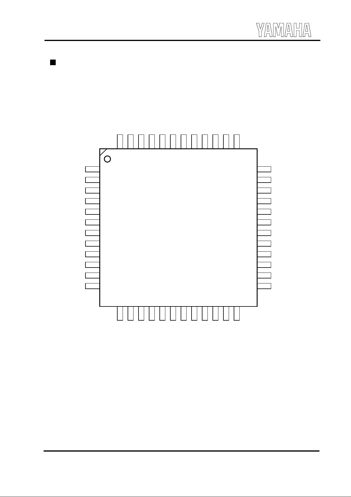
PIN CONFIGURATION
TEST
EAPD
CODEC ID1#
CODEC ID0#
(N.C.)
(N.C.)
AVss2
LNLVL_OUT_R
(N.C.)
LNLVL_OUT_L
AVdd2
MONO_OUT
48
47
46
45
44
43
42
41
40
39
38
37
DVdd1
XTL_IN
XTL_OUT
DVss1
SDATA_OUT
BIT_CLK
DVss2
SDATA_IN
DVdd2
SYNC
RESET#
PC_BEEP
10
11
12
24
LINE_IN_R
36
35
34
33
32
31
30
29
28
27
26
25
LINE_OUT_R
LINE_OUT_L
TEST
ENABLE
CAP4
CAP3
CAP2
CAP1
Vrefout
Vref
AVss1
AVdd1
1
2
3
4
5
6
7
8
9
13
14
15
16
17
18
19
20
21
22
23
MIC1
AUX_L
PHONE
AUX_R
VIDEO_L
CD_L
VIDEO_R
CD_R
CD_GND
MIC2
LINE_IN_L
48-Pin SQFP Top View
2
July 2, 1999
YMF752
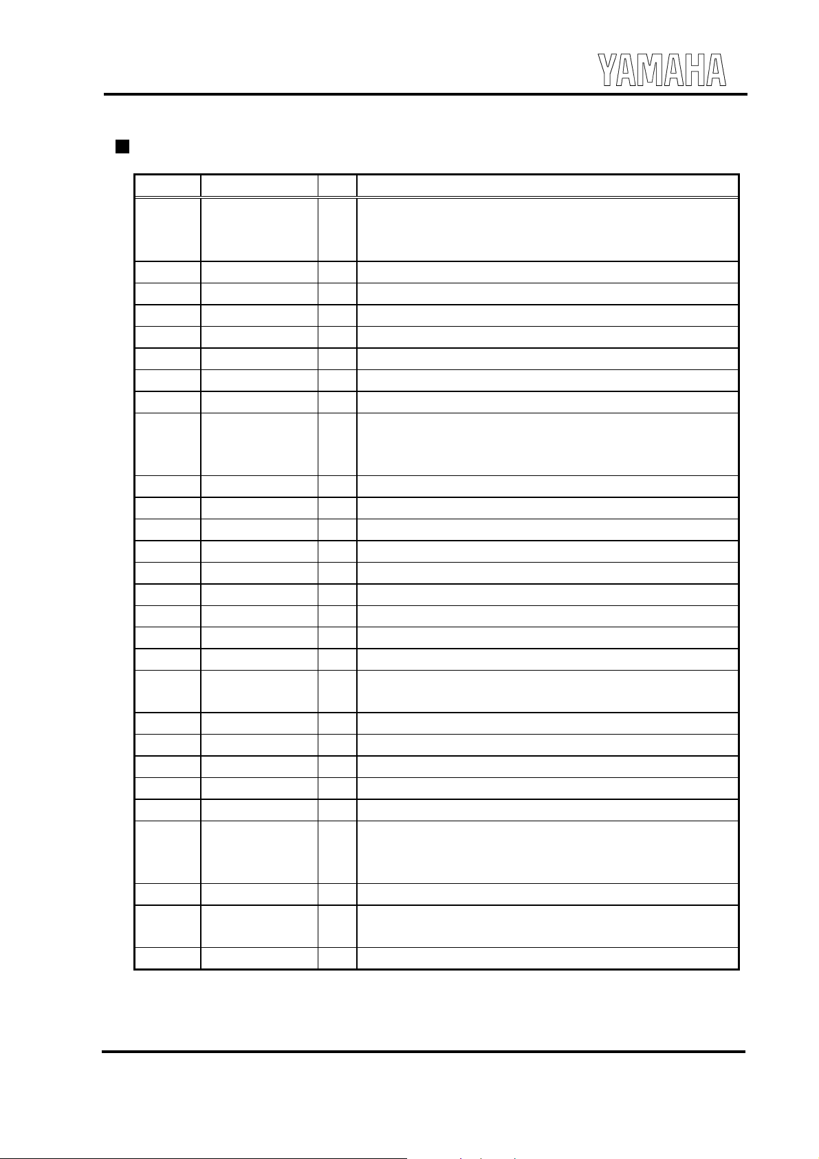
PIN DESCRIPTION
No. Name I/O Function
1 DVdd1 -
2 XTL_IN I 24.576MHz Clock Input
3 XTL_OUT O 24.576MHz Clock Output
4 DVss1 - Digital ground. Connect this pin to DVss2.
5 SDATA_OUT I AC’97 Serial Input Stream
6 BIT_CLK I/O AC’97 Bit Clock
7 DVss2 - Digital ground. Connect this pin to DVss1.
8 SDATA_IN O AC’97 Serial Output Stream
9 DVdd2 -
10 SYNC I SYNC Input (Fixed at 48kHz)
11 RESET# I Hardware Reset
12 PC_BEEP AI PC Speaker Beep
13 PHONE AI Telephony Input
14 AUX_L AI AUX Input Left Channel
15 AUX_R AI AUX Input Right Channel
16 VIDEO_L AI Video Audio Input Left Channel
17 VIDEO_R AI Video Audio Input Right Channel
18 CD_L AI CD Audio Input Left Channel
19 CD_GND AI
20 CD_R AI CD Audio Input Right Channel
21 MIC1 AI Microphone Input 1
22 MIC2 AI Microphone Input 2
23 LINE_IN_L AI Line Input Left Channel
24 LINE_IN_R AI Line Input Right Channel
25 AVdd1 -
26 AVss1 - Analog ground. Connect this pin to AVss2.
27 Vref AO
28 Vrefout AO Analog Reference Voltage Output
Digital power supply (+3.3V)
Connect to the digital ground with 0.1mF and 47mF capacitors.
Connect this pin to DVdd2.
Digital power supply (+3.3V)
Connect to the digital ground with 0.1mF and 47mF capacitors.
Connect this pin to DVdd1.
CD Audio Analog Ground
Connect this pin to CD Ground or Analog Ground.
Analog Power Supply (+5.0V)
Connect to the analog ground with 0.1mF and 47mF capacitors.
Connect this pin to AVdd2.
Analog Reference Voltage
Connect to the analog ground with 0.1mF and 10mF capacitors.
3
July 2, 1999
YMF752
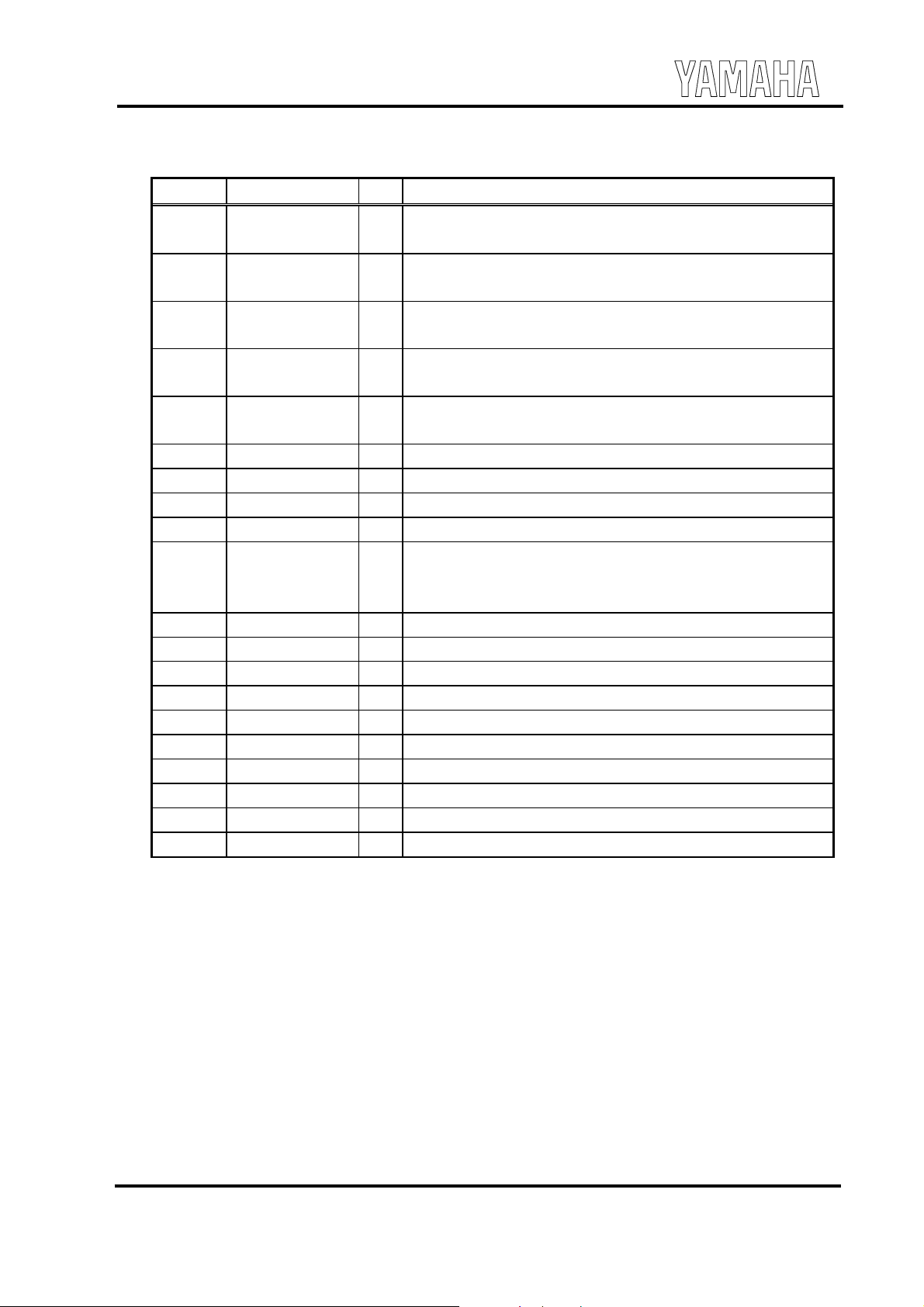
No. Name I/O Function
29 CAP1 A
30 CAP2 A
31 CAP3 A
32 CAP4 A
33 ENABLE I+
34 TEST I+ LSI Test Pin (Do not connect externally.)
35 LINE_OUT_L AO Line Output Left Channel
36 LINE_OUT_R AO Line Output Right Channel
37 MONO_OUT AO Monaural Output
38 AVdd2 -
39 LNLVL_OUT_L AO True LINE Level Output Left Channel
40 (N.C.) - Do not connect externally.
41 LNLVL_OUT_R AO True LINE Level Output Right Channel
42 AVss2 - Analog ground. Connect to Avss1.
43 (N.C.) - Do not connect externally.
44 (N.C.) - Do not connect externally.
45 CODEC ID0# I+ CODEC ID (Do not connect externally.)
46 CODEC ID1# I+ CODEC ID (Do not connect externally.)
47 EAPD O External Amplifier Power Down
48 TEST O LSI Test Pin (Do not connect externally.)
Note) AI: Analog Input Pin, AO: Analog Output Pin, I+: Input Pin with a Pull-up resistor
Capacitor Connection Pin
Connect to the analog ground with a 560pF capacitor.
Capacitor Connection Pin
Connect to the analog ground with a 560pF capacitor.
Capacitor Connection Pin
Connect to the analog ground with a 1000pF capacitor.
Capacitor Connection Pin
Connect to the analog ground with 0.1mF and 10mF capacitors.
Normally, do not connect externally.
In case of “low” level, YMF752 do not operate.
Analog power supply (+5.0V)
Connect to the digital ground with 0.1mF and 47mF capacitors.
Connect this pin to Avdd1.
4
July 2, 1999
YMF752
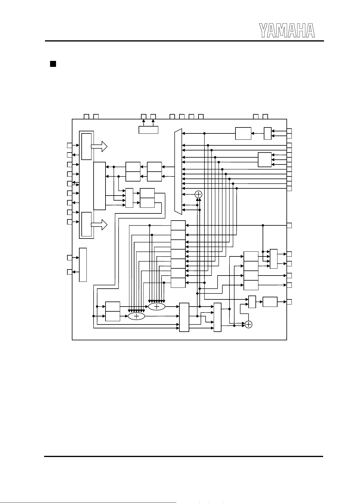
BLOCK DIAGRAM
DVdd(2)
DVss(2)
Vref
Vrefout
CAP4
CAP3
CAP2
CAP1
AVss(2)
AVdd(2)
ENABLE
EAPD
RESET#
SYNC
BIT_CLK
SDATA_OUT
SDATA_IN
CODEC ID0#
CODEC ID1#
XTL_IN
XTL_OUT
Power down
AC’97
digital
I/F
Volume
Timing Generator
VREF
Control
A/D
A/D
Record R
16step
Record L
16step
MUX
SRC
D/A
MUX
D/A
PC Beep
Left
16step
PHONE
32step
AUX
32step
VIDEO
32step
CD
32step
LINE
32step
MIC
32step
3D
MUX
Control
PCM L
32step
PCM R
32step
Right
0dB/
+20dB
CD Right
CD Left
Master L
Master R
L 32step
R 32step
32step
32step
LNLVL
LNLVL
MUX
BUF
Monaural
32step
MIC1
MUX
MUX
MIC2
LINE_IN_R
LINE_IN_L
CD_R
CD_GND
CD_L
VIDEO_R
VIDEO_L
AUX_R
AUX_L
PHONE
PC_BEEP
LINE_OUT_L
LINE_OUT_R
LNLVL_OUT_L
LNLVL_OUT_R
MONO_OUT
5
July 2, 1999
 Loading...