

Yamaha YMF744B Datasheet
YMF744B
Preliminary
DS-1S
OVERVIEW
YMF744B (DS-1S) is a high performance audio controller for the PCI Bus. DS-1S consists of two separated
functional blocks. One is the PCI Audio block and the other is the Legacy Audio block. PCI Audio block
allows Software Driver to handle maximum of 73 concurrent audio streams with the Bus Master DMA engine.
The PCI Audio Engine converts the sampling rate of each audio stream and the streams are mixed without
utilizing the CPU or causing system latency. By using the Software Driver from YAMAHA, PCI Audio
provides 64-voice XG wavetable synthesizer with Reverb and variation. It also supports DirectSound hardware
accelerator, Downloadable Sound (DLS) and DirectMusic accelerator.
Legacy Audio block supports FM Synthesizer, Sound Blaster Pro, MPU401 UART mode and Joystick
function in order to provide hardware compatibility for numerous PC games on real DOS without any software
driver. To achieve legacy DMAC compatibility on the PCI, DS-1S supports both PC/PCI and Distributed
DMA protocols. DS-1S also supports Serialized IRQ for legacy IRQ compatibility.
DS-1S supports the connection to AC’97 which provides high quality DAC, ADC and analog mixing, and it
can connect two AC’97s. In addition, it supports consumer IEC958, Audio Digital Interface (SPDIF), to
connect external audio equipment by digital.
FEATURES
• PCI 2.2 Compliant
• PC’98/PC’99 specification Compliant
• PCI Bus Power Management rev. 1.0 Compliant
(Support D0, D2 and D3 state)
• Supports clock run
• PCI Bus Master for PCI Audio
True Full Duplex Playback and Capture with
different Sampling Rate
Maximum 64-voice XG capital Wavetable
Synthesizer including GM compatibility
DirectSound Hardware Acceleration
DirectMusic Hardware Acceleration
Downloadable Sound (DLS) level-1
• Legacy Audio compatibility
FM Synthesizer
Hardware Sound Blaster Pro compatibility
MPU401 UART mode MIDI interface
Joystick
• Supports Serialized IRQ
• Supports PC/PCI and Distributed DMA for legacy
DMAC (8237) emulation
• Supports I
• Supports Consumer IEC958 Output (SPDIF OUT)
• Supports Consumer IEC958 Input (SPDIF IN)
• Supports AC’97 Interface (AC-Link) Revision 2.1
• AC’97 Digital Docking
• Supports 4-Channel Speaker
• Hardware Volume Control
• EEPROM Interface
• Single Crystal operation (24.576MHz)
• 3.3V Power supply (5V tolerant)
• 128-pin LQFP YMF744B-V : 0.5mm pin pitch
2
S serial input for Zoomed Video Port
YMF744B-R : 0.4mm pin pitch
The contents of this catalog are target specifications and are subject to change
without prior notice. When using this device, please recheck the specifications.
YAMAHA
CORPORATION
CATALOG No.:LSI-4MF744B00
YMF744B CATALOG
December 18, 1998
February 3, 1999

YMF744B
LOGOS
GENERAL MIDI logo is a trademark of Association of Musical Electronics Industry (AMEI),
and indicates GM system level 1 Compliant.
XG logo is a trademark of YAMAHA Corporation.
1. GM system level 1
GM system level 1 is a world standard format about MIDI synthesizer which provides voice arrangements
and MIDI functions.
2. XG
XG is a format about MIDI synthesizer that is proposed by YAMAHA, and keeps the upper compatibility of
GM system level 1. The good points are the voice arrangements kept extensively, a large number of the
voices, modification of the voices, 3 kinds of effects, and so on.
3. SONDIUS-XG
Products bearing the SONDIUS-XG logo are licensed under patents of Stanford University and YAMAHA
Corporation as listed on <http://www.sondius-xg.com>. The SONDIUS-XG produces acoustic sound
outputs by running a virtual simulation of the actual acoustic instrument operatio n. T herefore, it pr ovides
much more real-world acoustic sound outputs fundamentally different fr om the Wavetable sound generator
that simply processes the recorded acoustic sound sources only. The SONDIUS-XG adds the technology
of virtual acoustic sound to the XG format.
4. Sensaura
Sensaura is a technology which provides 3D positional audio and moving effect by HRTF (Head Related
Transfer Function) with 2 speakers or headphone. This feature makes it possible to enjoy invariable and
unchangeable sound feelings in all-positional area covering as wide as 360 degrees.
SONDIUS-XG logo is a trademark that Stanford University in the United States and
YAMAHA Corporation hold jointly.
Sensaura logo is a trad emark of Central Research Laboratories Limited.
-2-
February 3, 1999
YMF744B
PIN CONFIGURATION
YMF744B-V (0.5mm pin pitch)
AD27
AD26
PVDD2
AD25
AD24
CBE3#
IDSEL
AD23
PVSS4
AD22
AD21
AD20
AD19
AD18
AD17
AD16
CBE2#
PVSS3
FRAME#
IRDY#
TRDY#
DEVS EL#
PVDD1
STOP#
PERR#
SERR#
PAR
CBE1#
PVSS2
AD15
AD14
AD13
AD12
AD11
AD10
AD9
AD8
PVSS1
CBE0#
128
1
2
3
4
5
6
7
8
9
10
11
12
13
14
15
16
17
18
19
20
21
22
23
24
25
26
27
28
29
30
31
32
33
34
35
36
37
38
39
AD28
AD29
AD30
AD31
REQ#
127
40
PVSS5
126
41
125
42
124
43
123
44
122
45
GNT#
121
46
PCICLK
120
47
RST#
119
48
PVSS6
118
49
PVDD3
117
50
RESER VE0
116
51
INTA#
115
52
CVDD2
114
53
RESERV E1
113
54
GP7
112
55
GP6
111
56
GP5
110
57
GP4
109
58
GP3
108
59
GP2
107
60
GP1
106
61
GP0
105
62
TXD
104
63
RXD
103
102
101
100
99
98
97
96
95
94
93
92
91
90
89
88
87
86
85
84
83
82
81
80
79
78
77
76
75
74
73
72
71
70
69
68
67
66
65
64
TEST#
VDD2
VSS3
VDD1
CMCLK
CSDO
CBCLK
CSDI0
CSYNC
CRST#
VDD0
VSS2
RESE RVE2
RESE RVE3
CSDI2
DOCKEN#
VSS1
XI24
XO24
LOOPF
LVDD
CVDD1
ZVBCLK
ZVLRCK
ZVSDI
SPDI FOUT
SPDI FIN
IRQ11
IRQ10
IRQ9
IRQ7
IRQ5
GPIO2
GPIO1
GPIO0
RESE RVE8
RESE RVE9
RESER VE10
AD7
AD6
AD5
AD4
AD3
AD2
AD1
AD0
PVDD0
PVSS0
SERIRQ#
CVDD0
ROMDI
ROMDO/ VOLDW#
ROMSK/ VOLUP#
ROMCS
RESER VE14
RESER VE15
RESER VE16
PCGNT#
PCREQ#
CLKRUN#
RESER VE13
VSS0
RESER VE12
RESER VE11
128 Pin LQFP Top View
February 3, 1999
-3-
YMF744B
YMF744B-R (0.4mm pin pitch)
AD25
PVDD2
AD26
RST#
RESER VE0
PVDD3
REQ#
AD27
AD28
AD31
PVSS5
AD29
AD30
PVSS6
GNT#
PCICLK
RESE RVE1
CVDD2
INTA#
GP4
GP5
GP2
GP3
GP6
GP7
GP1
GP0
RXD
TXD
TEST#
VSS3
VDD2
AD24
CBE3#
IDSEL
AD23
PVSS4
AD22
AD21
AD20
AD19
AD18
AD17
AD16
CBE2#
PVSS3
FRAME#
IRDY#
TRDY#
DEVSEL#
PVDD1
STOP#
PERR#
SERR#
PAR
CBE1#
PVSS2
AD15
AD14
AD13
AD12
AD11
AD10
AD9
1
2
3
4
5
6
7
8
9
10
11
12
13
14
15
16
17
18
19
20
21
22
23
24
25
26
27
28
29
30
31
32
125
126
127
128
3334353637
102
59
101
60
999897
100
62
61
63
64
96
95
94
93
92
91
90
89
88
87
86
85
84
83
82
81
80
79
78
77
76
75
74
73
72
71
70
69
68
67
66
65
VDD1
CMCLK
CSDO
CBCLK
CSDI0
CSYNC
CRST#
VDD0
VSS2
RESERVE2
RESERVE3
CSDI2
DOCKEN#
VSS1
XI24
XO24
LOOPF
LVDD
CVDD1
ZVBCLK
ZVLRCK
ZVSDI
SPDIFOUT
SPDIFIN
IRQ11
IRQ10
IRQ9
IRQ7
IRQ5
GPIO2
GPIO1
GPIO0
108
107
109
110
111
112
113
114
115
116
117
118
119
120
121
122
123
124
54
53
52
51
50
49
48
47
46
45
44
43
42
41
40
39
38
55
105
56
57
103
58
104
106
AD8
AD7
AD6
AD5
AD4
AD3
AD2
AD1
PVSS1
CBE0#
PVDD0
AD0
PVSS0
SERIRQ#
CVDD0
ROMDI
ROMDO/ VOLDW#
ROMSK/ VOLUP#
ROMCS
RESER VE16
RESER VE15
RESER VE14
PCGNT#
PCREQ#
CLKRUN#
VSS0
RESERV E8
RESERV E9
RESER VE11
RESER VE12
RESER VE13
RESER VE10
128 Pin LQFP Top View
February 3, 1999
-4-
YMF744B
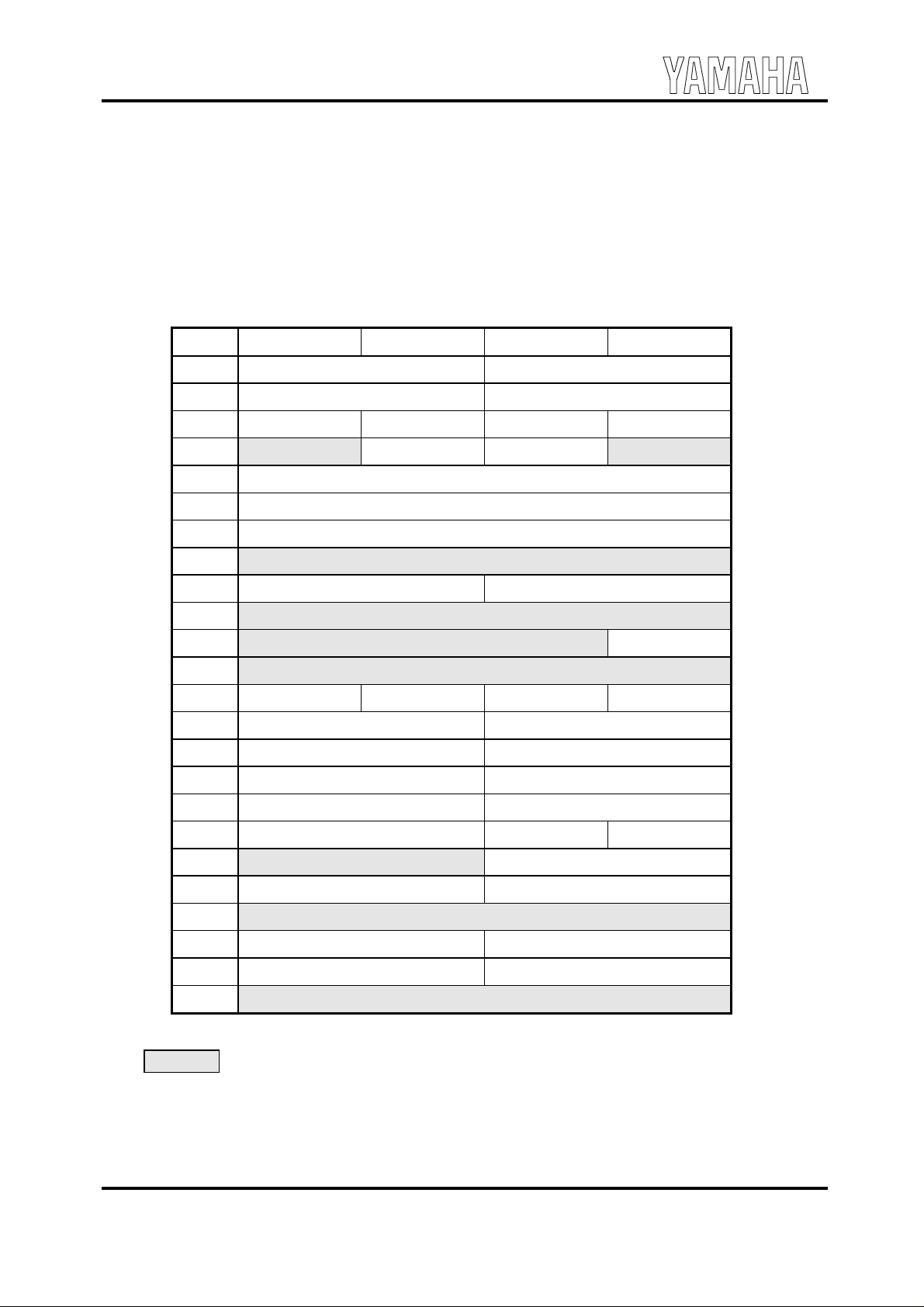
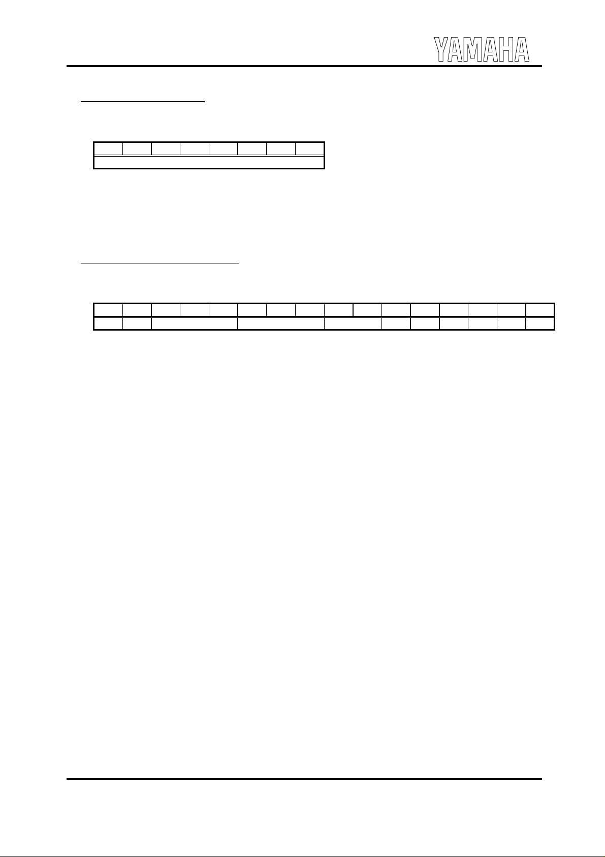
PIN DESCRIPTION
1. PCI Bus Interface (54-pin)
Name I/O Type Size Function
PCICLK I P PCI Clock
RST# I P Reset
AD[31:0] IO Ptr Address / Data
C/BE[3:0]# IO Ptr Command / Byte Enable
PAR IO Ptr Parity
FRAME# IO Pstr Frame
IRDY# IO Pstr Initiator Ready
TRDY# IO Pstr Target Ready
STOP# IO Pstr Stop
IDSEL I P ID Select
DEVSEL# IO Pstr Device Select
REQ# O Ptr PCI Request
GNT# I P PCI Grant
PCREQ# O Ptr PC/PCI Request
PCGNT# I P PC/PCI Grant
PERR# IO Pstr Parity Error
SERR# O Pod System Error
INTA# O Pod Interrupt signal output for PCI bus
SERIRQ# IO Ptr Serialized IRQ
CLKRUN# IO Ptr Clock Run
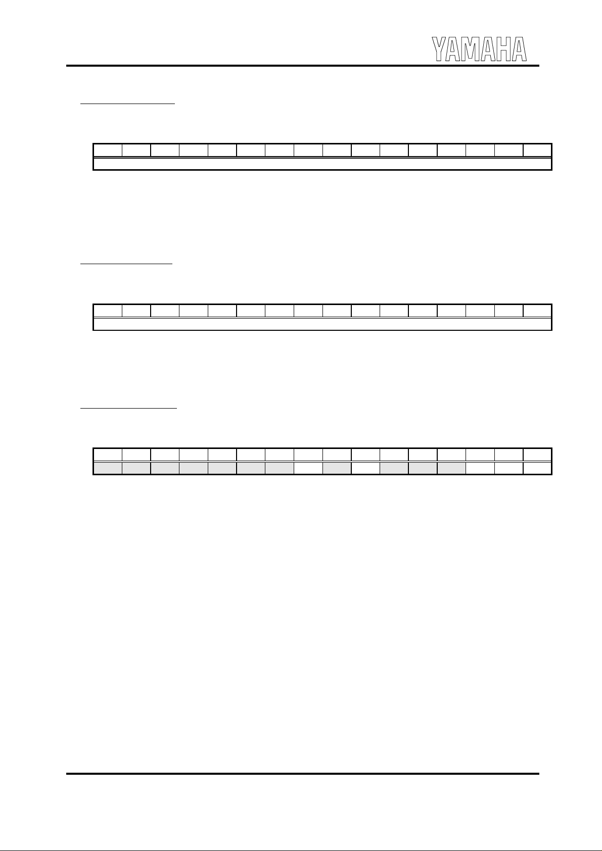
2. AC’97 Interface (8-pin)
Name I/O Type Size Function
CRST# O T 6mA Reset signal for AC’97
CMCLK O C 6mA Master Clock for AC’97 (24.576MHz)
CBCLK I T - AC-link: Bit Clock for AC’97 audio data
CSDO O T 6mA AC-link: AC’97 Serial audio output data
CSYNC O T 6mA AC-link: AC’97 Synchronized signal
CSDI0 I T - AC-link: AC’97 Serial audio input data (Primary)
CSDI2 I Tup - AC-link: AC’97 Serial audio input data (Secondary)
DOCKEN# I Tup - Docking Enable
February 3, 1999
-5-
YMF744B
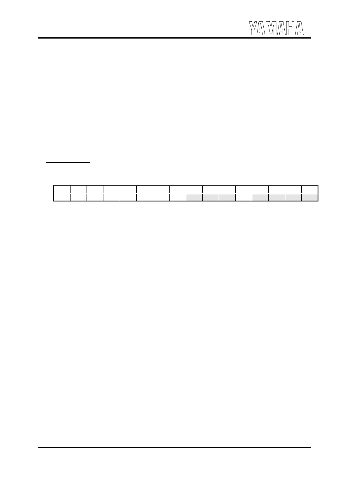
3. External Audio Interface (5-pin)
Name I/O Type Size Function
SPDIFOUT O T 2mA Digital Audio Interface output
SPDIFIN I Tup - Digital Audio Interface input
ZVBCLK I Tup - Zoomed Video Port Bit Clock
ZVLRCK I Tup - Zoomed Video Port L/R Clock
ZVSDI I Tup - Zoomed Video Port Serial Data
4. Legacy Device Interface (15-pin)
Name I/O Type Size Function
Interrupt5 of Legacy Audio
IRQ5 O Ttr 12mA
IRQ7 O Ttr 12mA Interrupt7 of Legacy Audio
IRQ9 O Ttr 12mA Interrupt9 of Legacy Audio
IRQ10 O Ttr 12mA Interrupt10 of Legacy Audio
IRQ11 O Ttr 12mA Interrupt11 of Legacy Audio.
GP[3:0] I A - Game Port
GP[7:4] I Tup - Game Port
RXD I Tup - MIDI Data Receive
TXD O T 2mA MIDI Data Transfer
It is directly connected to the interrupt signal of
System I/O chip.
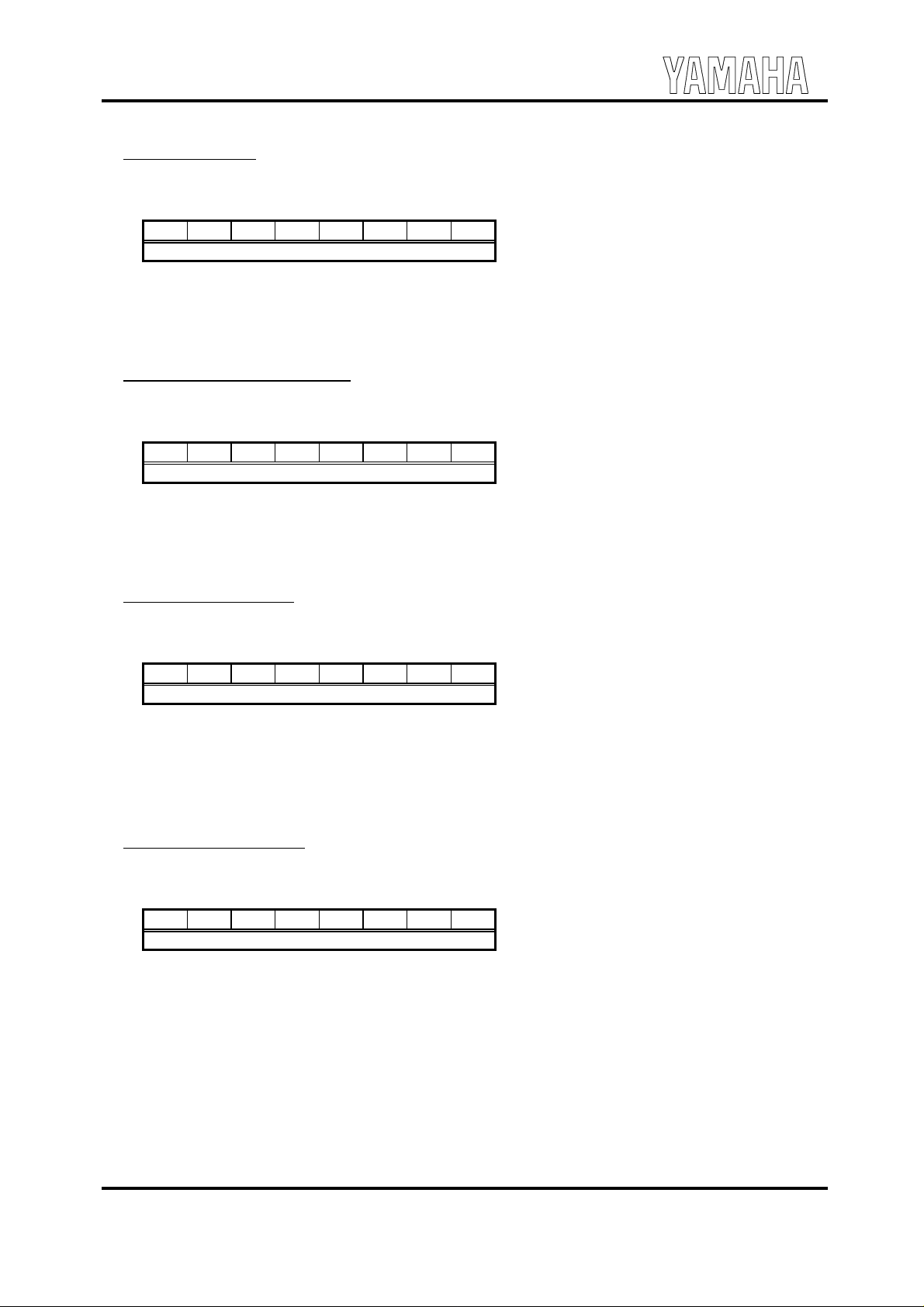
5. Miscellaneous (11-pin)
Name I/O Type Size Function
ROMCS O T 2mA Chip select for external EEPROM
ROMSK / VOLUP# IO Tup 2mA
ROMDO / VOLDW# IO Tup 2mA
ROMDI I Tup - Serial data input for external EEPROM
XI24 I C - 24.576 MHz Crystal
XO24 O C - 24.576 MHz Crystal
LOOPF I A - Capacitor for PLL
GPIO[2:0] IO Tup 2mA
TEST# I Tup - LSI Test pin (Do not connect externally.)
Serial clock for external EEPROM
or Hardware Volume (Up)
Serial data output for external EEPROM
or Hardware Volume (Down)
General purpose Input / Output
GPIO2 can use for a reset pin of Secondary AC’97.
February 3, 1999
-6-
YMF744B
6. Power Supply (22-pin)
Name I/O Type Size Function
PVDD[3:0] - - - 3.3V Power supply for PCI Bus Interface
PVSS[6:0] - - - Ground for PCI Bus Interface
CVDD[2:0] - - - 3.3V Power supply for Core logic
VDD[2:0] - - - 3.3V Power supply
VSS[3:0] - - - Ground
LVDD - - - 3.3V Power supply for PLL Filter
7. Reserve Pin (13-pin)
Name I/O Type Size Function
RESERVE0 O Pod RESERVE[3:2] I Tup RESERVE[16:8,1] - - -
Reserve pins (Do not connect externally.)
TYPE
T : TTL A : Analog Ptr : Tri-State PCI
Ttr : Tri-State TTL C : CMOS Pstr : Sustained Tri-Sate PCI
Tup : Pull up (Max. 300kohm) TTL P : PCI Pod : Open Drain PCI
-7-
February 3, 1999
YMF744B
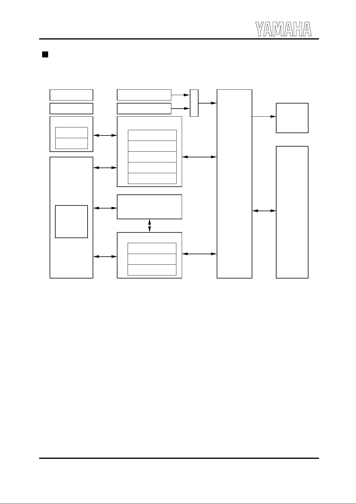
gReg
g
BLOCK DIAGRAM
EEPROM I/F
GPIO
PCI Side Band
PC/PCI
S-IRQ
PCI
Interfa ce
Aud io
Function
Confi
ister
SPDIF Input
ZV Port
Legacy Audio
FM Synthesizer
SB Pro
D-DMA Engine
MPU401
Joystick
PCI Bus Master
DMA Controller
PCI Native Audio
XG Synthesizer
DirectSound Acc.
Selector
SPDIF
Output
SRC
Samplin
Converter
AC-Link
Inte rfa ce
Revision2.1
Wave In/Out
February 3, 1999
-8-
YMF744B
FUNCTION OVERVIEW
1. PCI INTERFACE
DS-1S supports the PCI bus interface and complies to PCI revision 2.2.
1-1. PCI Bus Command
DS-1S supports the following PCI Bus commands.
1-1-1. Target Device Mode
C/BE[3:0]# Command
0000Interrupt Acknowledge (not support)
0001Special Cycle (not support)
0010I/O Read
0011I/O Write
0100reserved
0101reserved
0110Memory Read
0111Memory Write
1000reserved
1001reserved
1010Configuration Read
1011Configuration Write
1100Memory Read Multiple (not support)
1101Dual Address Cycle (not support)
1110Memory Read Line (not support)
1111Memory Write and Invalidate (not support)
DS-1S does not assert DEVSEL# when accessed with commands that are indicated as (not supported) or
reserved.
1-1-2. Master Device Mode
C/BE[3:0]# Command
0110Memory Read
0111Memory Write
When DS-1S becomes a Master Device, it generates only memory write and read cycle commands.
-9-
February 3, 1999
YMF744B
1-2. PCI Configuration Register
In addition to the Configuration Register defined by PCI Revision 2.2, DS-1S provides proprietary PCI
Configuration Registers in order to control legacy audio functio n, such as FM Synthesizer, Sound Blaster Pro,
MPU401 and Joystick. These additional registers are configured by BIOS or the configuration software
from YAMAHA Corporation.
The following shows the overview of the PCI Configuration Register.
Offset b[31..24] b[23..16] b[15..8] b[7..0]
00-03h Device ID Vendor ID
04-07h Status Command
08-0Bh Base Class Code Sub Class Code Programming IF Revision ID
0C-0Fh Reserved Header Type Latency Timer Reserved
10-13h PCI Audio Memory Base Addres s
14-17h Legacy Audio I/O Base Address (Dummy for S B, FM, MPU, D-DMA)
18-1Bh Legac y A udi o I/O Base Address (Dummy for Joysti ck)
1C-2Bh Reserved
2C-2Fh Subsystem ID Subsystem Vendor ID
30-33h Reserved
34-37h Reserved Cap Pointer
38-3Bh Reserved
3C-3Fh Maximum Latency Minimum Grant Interrupt Pin Interrupt Line
40-43h Extended Legacy Audio Control Legacy Audio Control
44-47h Subsystem ID Write Subsystem Vendor ID Write
48-4Bh DS-1S Power Control 1 DS-1S Control
4C-4Fh DS-1S Power Control 2 D-DMA Slave Configuration
50-53h Power Management Capabilities Next Item Pointer Capability ID
54-57h Res erved Power Management Control / Status
58-5Bh DS-1S Secondary AC’97 P ower Control ACPI Mode
5C-5Fh Reserved
60-63h Sound Blaster Base Address FM Synthesizer Base Address
64-67h Joystick Base Address MPU401 Base Address
68-FFh Res erved
Reserved registers are hardwired to “0”. All data written to these registers are discarded. The values
read from these registers are all zero.
DS-1S can be accessed by using any bus width, 8-bit, 16-bit or 32-bit.
February 3, 1999
-10-
YMF744B
00-01h: Vendor ID
Read Only
Default: 1073h
Access Bus Width: 8, 16, 32-bit
b15 b14 b13 b12 b11 b10 b9 b8 b7 b6 b5 b4 b3 b2 b1 b0
Vendor ID
b[15:0]........Vendor ID
This register contains the YAMAHA Vendor ID registered in Revision 2.2. This register is hardwired to
1073h.
02-03h: Device ID
Read Only
Default: 0010h
Access Bus Width: 8, 16, 32-bit
b15 b14 b13 b12 b11 b10 b9 b8 b7 b6 b5 b4 b3 b2 b1 b0
Device ID
b[15:0]........Device ID
This register contains the Device ID of DS-1S. This register is hardwired to 0010h.
04-05h: Command
Read / Write
Default: 0000h
Access Bus Width: 8, 16, 32-bit
b15 b14 b13 b12 b11 b10 b9 b8 b7 b6 b5 b4 b3 b2 b1 b0
- - - - - - - SER - PER - - - BME MS IOS
b0................IOS: I/O Space
This bit is a dummy one that is capable of writing. This bit indicates for BIOS or OS that DS-1S
includes I/O devices.
b1................MS: Memory Space
This bit enables DS-1S to response to Memory Space Access.
“0”: DS-1S ignores Memory Space Access. (default)
“1”: DS-1S responds to Memory Space Access.
b2................BME: Bus Master Enable
This bit enables DS-1S to act as a master device on the PCI bus.
“0”: Do not set DS-1S to be the master device. (default)
“1”: Set DS-1S to be the master device.
-11-
February 3, 1999
YMF744B
b6................PER: Parity Error Response
This bit enables DS-1S responses to Parity Error.
“0”: DS-1S ignores all parity errors.
“1”: DS-1S performs error operation when DS-1S detects a parity error.
b8................SER: SERR# Enable
This bit enables DS-1S to drive SERR#.
“0”: Do not drive SERR#. (default)
“1”: Drives SERR# when DS-1S detects an Address Parity Error on normal target cycle or a Data Parity
Error on special cycle.
06-07h: Status
Read / Write Clear
Default: 0210h
Access Bus Width: 8, 16, 32-bit
b15 b14 b13 b12 b11 b10 b9 b8 b7 b6 b5 b4 b3 b2 b1 b0
DPE SSE RMA RTA STA DEVT DPD - - - CAP - - - -
b4................CAP: Capability (Read Only)
This bit indicates that DS-1S supports the capability register. This bit is read only. When 58-59h :
ACPI Mode register, ACPI bit is “0”, the bit is “1”. When ACPI bit is “1”, the bit is “0”.
b8................DPD: Data Parity Error Detected
This bit indicates that DS-1S detects a Data Parity Error during a PCI master cycle.
b[10:9] ........DEVT: DEVSEL Timing
This bit indicates that the decoding speed of DS-1S is Medium.
b11..............STA: Signaled Target Abort
This bit indicates that DS-1S terminates a transaction with Target Abort during a target cycle.
b12..............RTA: Received Target Abort
This bit indicates that a transaction is terminated with Target Abort while DS-1S is in the master memory
cycle.
b13..............RMA: Received Master Abort
This bit indicates that a transaction is terminated with Master Abort while DS-1S is in the master memory
cycle.
b14..............SSE: Signaled System Error
This bit indicates that DS-1S asserts SERR#.
b15..............DPE: Detected Parity Error
This bit indicates that DS-1S detects Address Parity Error or Data Parity Error during a transaction.
February 3, 1999
-12-
YMF744B
08h: Revision ID
Read Only
Default: 02h
Access Bus Width: 8, 16, 32-bit
b7 b6 b5 b4 b3 b2 b1 b0
Revision ID
b[7:0]..........Revision ID
This register contains the revision number of DS-1S. This re giste r is hardwired to 02h.
09h: Programming Interface
Read Only
Default: 00h
Access Bus Width: 8, 16, 32-bit
b7 b6 b5 b4 b3 b2 b1 b0
Programming Interf ace
b[7:0]..........Programming Interface
This register indicates the programming interface of DS-1S. This register is hardwired to 00h.
0Ah: Sub-class Code
Read Only
Default: 01h
Access Bus Width: 8, 16, 32-bit
b7 b6 b5 b4 b3 b2 b1 b0
Sub-class Code
b[7:0]..........Sub-class Code
This register indicates the sub-class of DS-1S. T his register is hardwired to 01h. DS-1S belongs to the
Audio Sub-class.
0Bh: Base Class Code
Read Only
Default: 04h
Access Bus Width: 8, 16, 32-bit
b7 b6 b5 b4 b3 b2 b1 b0
Base Class Code
b[7:0]..........Base Class Code
This register indicates the base class of DS-1S. This register is hardwired to 04h. DS-1S belongs to
the Multimedia Base Class.
February 3, 1999
-13-
YMF744B
0Dh: Latency Timer
Read / Write
Default: 00h
Access Bus Width: 8, 16, 32-bit
b7 b6 b5 b4 b3 b2 b1 b0
Latency Timer
b[7:0]..........Latency Timer
When DS-1S becomes a Bus Master device, this register indicates the initial value of the Master Latency
Timer.
0Eh: Header Type
Read Only
Default: 00h
Access Bus Width: 8, 16, 32-bit
b7 b6 b5 b4 b3 b2 b1 b0
Header Type
b[7:0]..........Header Type
This register indicates the device type of DS-1S. This is hardwired to 00h.
10-13h: PCI Audio Memory Base Address
Read / Write
Default: 00000000h
Access Bus Width: 8, 16, 32-bit
b15 b14 b13 b12 b11 b10 b9 b8 b7 b6 b5 b4 b3 b2 b1 b0
MBA - - - - - - - - - - - - - - -
b31 b30 b29 b28 b27 b26 b25 b24 b23 b22 b21 b20 b19 b18 b17 b16
MBA (higher)
b[31:15]......MBA: Memory Base Address
This register indicates the physical Memory Base address of the PCI Audio registers in DS-1S. The base
address can be located anywhere in the 32-bit address space. Data in the DS-1S register is not
prefetchable.
Size of the register to be mapped into the memory space is 32,768 bytes.
-14-
February 3, 1999
YMF744B
14-17h: Legacy Audio I/O Base Address (Dummy for SB, FM, MPU, D-DMA)
Read / Write
Default: 00000001h
Access Bus Width: 8, 16, 32-bit
b15 b14 b13 b12 b11 b10 b9 b8 b7 b6 b5 b4 b3 b2 b1 b0
IOBASE0 - - - - - I/O
b31 b30 b29 b28 b27 b26 b25 b24 b23 b22 b21 b20 b19 b18 b17 b16
- - - - - - - - - - - - - - - -
b0................IO (Read Only)
This bit indicates that the base address is assigned to I/O. This bit is hardwired to “1”.
b[15:6]........IOBASE0
This register is used so that the OS may secure I/O resources for Sound Blaster Pro, FM Synthesizer,
MPU401 and D-DMA controller. Because this register is a dummy one, each for the I/O addresses of
the above blocks is assigned with the I/O addresses set to 4C-4Dh and 60-65h respectively by the software
driver.
18-1Bh: Legacy Audio I/O Base Address (Dummy for Joystick)
Read / Write
Default: 00000001h
Access Bus Width: 8, 16, 32-bit
b15 B14 b13 b12 b11 b10 b9 b8 b7 b6 b5 b4 b3 b2 b1 b0
IOBASE1 - I/O
b31 B30 b29 b28 b27 b26 b25 b24 b23 b22 b21 b20 b19 b18 b17 b16
- - - - - - - - - - - - - - - -
b0................IO (Read Only)
This bit indicates that the base address is assigned to I/O. This bit is hardwired to “1”.
b[15:2]........IOBASE1
This register is used so that the OS may secure I/O resource for the joystick port. Because this register is
a dummy one, the joystick I/O address is assigned with the I/O address set to 66-67h by the software
driver.
-15-
February 3, 1999
YMF744B
2C-2Dh: Subsystem Vendor ID
Read Only
Default: 1073h
Access Bus Width: 8, 16, 32-bit
b15 b14 b13 b12 b11 b10 b9 b8 b7 b6 b5 b4 b3 b2 b1 b0
Subsystem Vendor ID
b[15:0]........Subsystem Vendor ID
This register contains the Subsystem Vendor ID. In genera l, this ID is used to distinguish adapters or
systems made by different IHVs using the same chip by the same vendor. This register is read only. To
write the IHV’s Vendor ID, use 44-45h (Subsystem Vendor ID Write Register). IHVs must change this
ID to their Vendor ID in the BIOS POST routine.
In case of the system such as Sound Card which BIOS can not control, this ID can be changed by
connecting EEPROM externally. Then, Subsystem Vendor ID Write Register is invalid.
In case EEPROM is not externally, the default value is the YAMAHA's Vendor ID, 1073h.
2E-2Fh: Subsystem ID
Read Only
Default: 0010h
Access Bus Width: 8, 16, 32-bit
b15 b14 b13 b12 b11 b10 b9 b8 b7 b6 b5 b4 b3 b2 b1 b0
Subsystem ID
b[15:0]........Subsystem ID
This register contains the Subsystem ID. In general, this ID is used to distinguish adapter s or systems
made by different IHVs using the same chip by the same vendor. This register is read only. T o write
the IHV's Device ID, use 46-47h (Subsystem ID Write Register). IHVs must change this ID to their ID
in the BIOS POST routine.
In case of the system such as Sound Card which BIOS can not control, this ID can be changed by
connecting EEPROM externally. Then, Subsystem ID Write Register is invalid.
In case EEPROM is not externally, the default value is the YAMAHA's Device ID, 0010h.
-16-
February 3, 1999
YMF744B
34h: Capability Register Pointer
Read Only
Default: 50h
Access Bus Width: 8, 16, 32-bit
b7 b6 b5 b4 b3 b2 b1 b0
Capability Register Pointer
b[7:0]..........Capability Register Pointer
This register indicates the offset address of the Capabilities register in the PCI Configuration register
when 58-59h: ACPI Mode register, ACPI bit is “0”. DS-1S provides PCI Bus Power Management
registers as the capabilities. The Power Management registers are mapped to 50h - 57h in the PCI
Configuration register, and this register indicates “50h”.
When ACPI bit is “1”, this register indicates “00h”.
3Ch: Interrupt Line
Read / Write
Default: 00h
Access Bus Width: 8, 16, 32-bit
b7 b6 b5 b4 b3 b2 b1 b0
Interrupt Line
b[7:0]..........Interrupt Line
This register indicates the interrupt channel that INTA# is assigned to.
3Dh: Interrupt Pin
Read Only
Default: 01h
Access Bus Width: 8, 16, 32-bit
b7 b6 b5 b4 b3 b2 b1 b0
Interrupt Pin
b[7:0]..........Interrupt Pin
DS-1S supports INTA# only. This register is hardwired to 01h.
3Eh: Minimum Grant
Read Only
Default: 05h
Access Bus Width: 8, 16, 32-bit
b7 b6 b5 b4 b3 b2 b1 b0
Minimum Grant
b[7:0]..........Minimum Grant
This register indicates the length of the burst period required by DS-1S.
This register is hardwired to 05h.
-17-
February 3, 1999
YMF744B
3Fh: Maximum Latency
Read Only
Default: 19h
Access Bus Width: 8, 16, 32-bit
b7 b6 b5 b4 b3 b2 b1 b0
Maximum Latency
b[7:0]..........Maximum Latency
This register indicates how often DS-1S generates the Bus Master Request.
This register is hardwired to 19h.
40-41h: Legacy Audio Control
Read / Write
Default: 907Fh
Access Bus Width: 8, 16, 32-bit
b15 b14 b13 b12 b11 b10 b9 b8 b7 b6 b5 b4 b3 b2 b1 b0
LAD SIEN MPUIRQ SBIRQ SDMA I/O MIEN MEN GPEN FMEN SBEN
b0................SBEN: Sound Blaster Enable
This bit enables the mapping of the Sound Blaster Pro block in the I/O space specified by the SBIO bits,
when LAD is set to “0”. The FM Synthesizer registers can be accessed via SB I/O space, while the SB
block is enabled, even if FMEN is set to “0”.
“0”: Disable the mapping of the SB block to the I/O space
“1”: Enable the mapping of the SB block to the I/O space (default)
b1................FMEN: FM Synthesizer Enable
This bit enables the mapping of the FM Synthesizer block in the I/O space specified by the FMIO bits,
when LAD is set to “0”. FM Synthesizer registers can be accessed via SB I/O space, while the SB block
is enabled, even if FMEN is set to “0”.
“0”: Disable the mapping of the FM Synthesizer block to the FMIO space
“1”: Enable the mapping of the FM Synthesizer block to the FMIO space (default)
After setting FMEN to “1”, about 100 msec is necessary before accessing these I/O space.
b2................GPEN: Gameport Enable
This bit enables the mapping of the Joystick block in the I/O space specified by the JSIO bits, when LAD
is set to “0”.
“0”: Disable the mapping of the Joystick block
“1”: Enable the mapping of the Joystick block (default)
b3................MEN: MPU401 Enable
This bit enables the mapping of the MPU401 block in the I/O space specified by the MPUIO bits, when
LAD is set to “0”.
“0”: Disable the mapping of the MPU401 block
“1”: Enable the mapping of the MPU401 block (default)
February 3, 1999
-18-
 Loading...