

Page 1
YMF740C
DS-1L
OVERVIEW
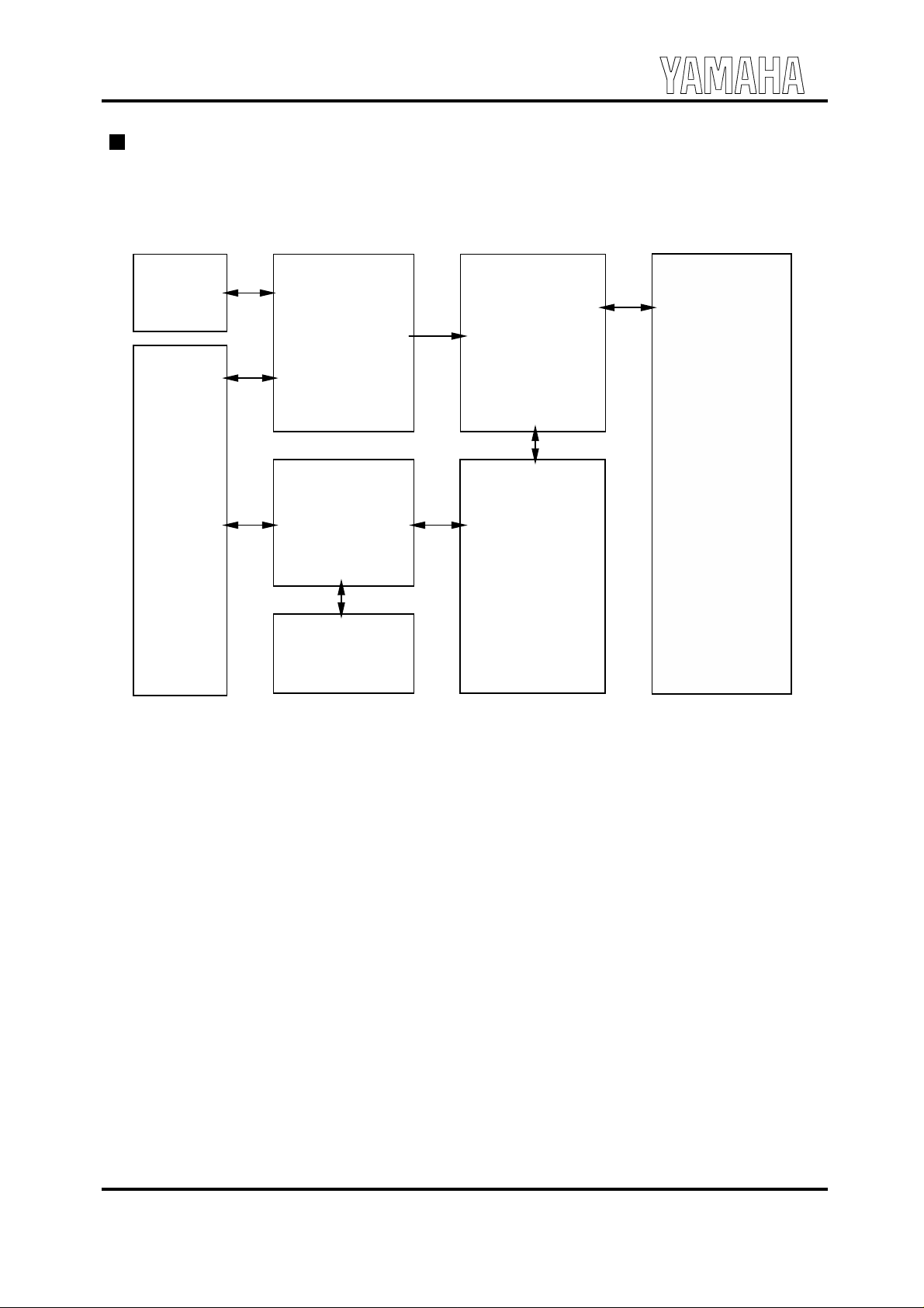
YMF740C (DS-1L) is a high performance audio controller for the PCI Bus. DS-1L consists of two separated
functional blocks. One is the PCI Audio block and the other is the Legacy Audio block. PCI Audio block
allows Software Driver to handle maximum of 41 concurrent audio streams with the Bus Master DMA engine.
The PCI Audio Engine converts the sampling rate of each audio stream and the streams are mixed without
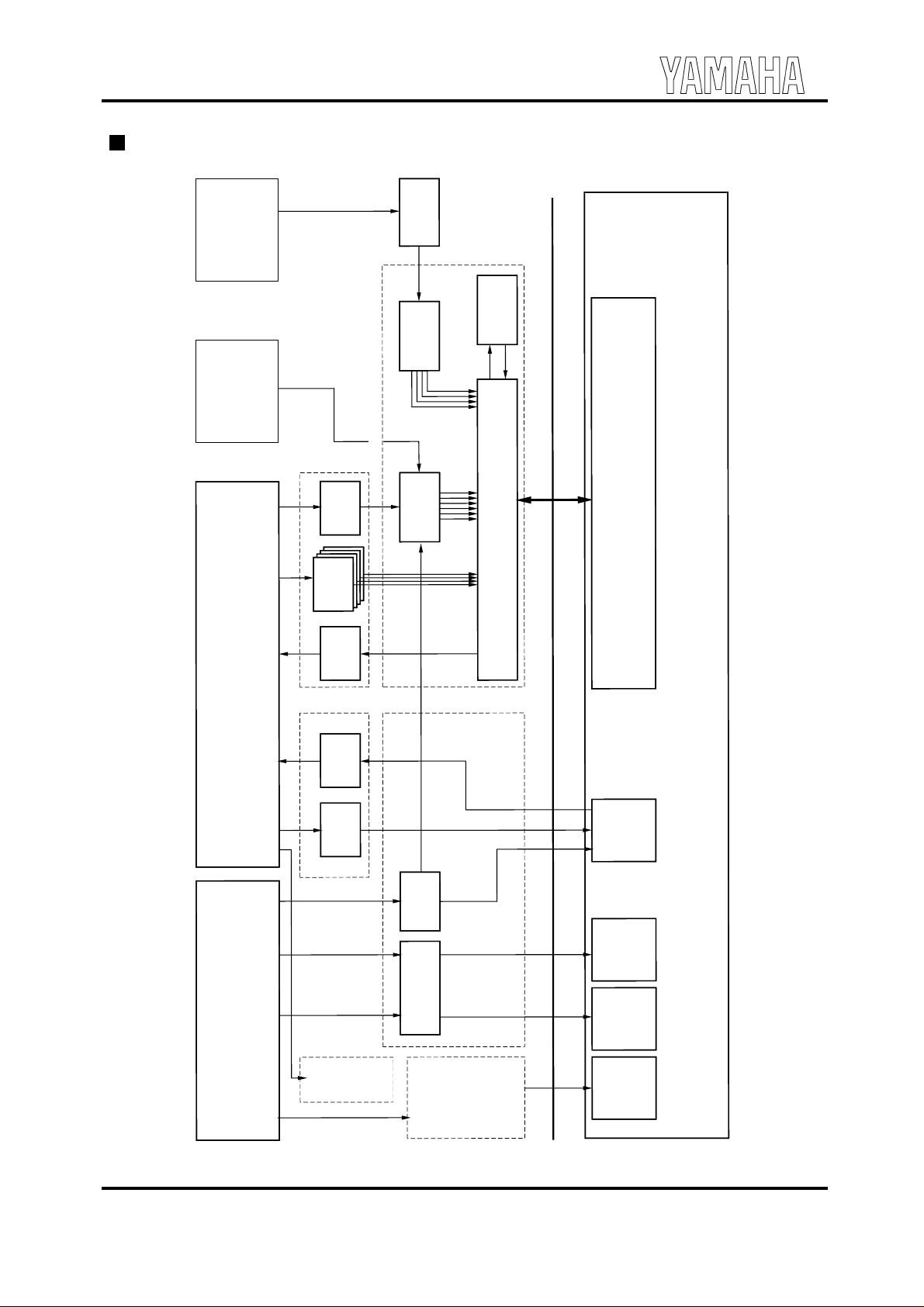
utilizing the CPU or causing system latency. By using the Software Driver from YAMAHA, PCI Audio
provides 32-voice XG wavetable synthesizer with Reverb and variation. It also supports DirectSound hardware
accelerator, Downloadable Sound (DLS) and DirectMusic accelerator.
Legacy Audio block supports FM Synthesizer, Sound Blaster Pro, MPU401 UART mode and Joystick
function in order to provide hardware compatibility for numerous PC games on real DOS without any software
driver. To achieve legacy DMAC compatibility on the PCI, DS-1L supports PC/PCI protocols.
DS-1L supports the connection to AC’97 which provides high quality DAC, ADC and analog mixing.
FEATURES
• PCI 2.1 Compliant
• PC’97/PC’98 specification Compliant
• PCI Bus Power Management rev. 1.0 Compliant
(Support D0, D2 and D3 state)
• PCI Bus Master for PCI Audio
True Full Duplex Playback and Capture with
different Sampling Rate
Maximum 32-voice XG capital Wavetable
Synthesizer including GM compatibility
DirectSound Hardware Acceleration
DirectMusic Hardware Acceleration
Downloadable Sound (DLS) level-1
• Supports PC/PCI DMA for legacy DMAC (8237)
emulation
• Legacy Audio compatibility
FM Synthesizer
Hardware Sound Blaster Pro compatibility
MPU401 UART mode MIDI interface
Joystick
• Supports AC’97 Interface (AC-Link)
• Hardware Volume Control
• Single Crystal operation (24.576MHz)
• 5V Power supply for I/O. 3.3V Power supply for
Internal core logic
• 144-pin LQFP (YMF740C-V)
GENERAL MIDI logo is a trademark of Associat ion of Musical Electronics Industry (AMEI),
and indicates GM system level 1 Compliant.
XG logo is a trademark of YAMAHA Corporation.
YAMAHA
CORPORATION
YMF740C CATALOG
CATALOG No.:LSI-4MF740C20
September 21, 1998
January 14, 1999
Page 2
YMF740C
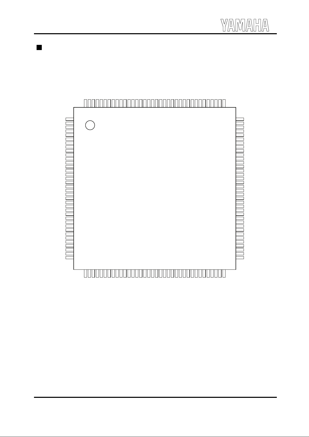
PIN CONFIGURATION
YMF740C-V
TEST2#
GP2
GP0
GP3
GP1
GREF
142
GP4
GP5
GP6
GP7
RXD
TXD
VOLDW#
VOLUP#
VDD5
VDD3
VSS
VSS
IRQ5
IRQ7
IRQ9
IRQ10
IRQ11
INTA#
VSS
RST#
VDD5
PVSS
PCICLK
PVDD
GNT#
REQ#
AD31
AD30
AD29
PVSS
AD28
AD27
AD26
PVSS
AD25
AD24
10
11
12
13
14
15
16
17
18
19
20
21
22
23
24
25
26
27
28
29
30
31
32
33
34
35
36
144
1
2
3
4
5
6
7
8
9
37
143
38
39
141
40
140
41
139
42
TEST0#
TEST1#
NC
138
136
137
44
43
45
LVSS
LOOPF1
134
135
46
47
LOOPF0
NC
LVDD
132
133
131
48
50
49
VDD5
TEST4#
XO24
128
130
129
52
51
53
XI24
VSS
126
127
54
55
VSS
125
56
VDD3
NC
124
123
58
57
TEST6#
TEST5#
TEST7#
122
120
121
60
59
61
CMCLK
CSDO
118
119
62
63
CBCLK
CSDI
117
116
64
65
CRST#
CSYNC
115
114
66
67
TEST3#
NC
NC
113
111
112
68
70
69
NC
110
71
NC
109
72
108
107
106
105
104
103
102
101
100
99
98
97
96
95
94
93
92
91
90
89
88
87
86
85
84
83
82
81
80
79
78
77
76
75
74
73
NC
NC
NC
NC
NC
NC
NC
NC
VSS
VSS
VDD3
VDD5
PVDD
NC
PCREQ#
PCGNT#
NC
AD0
AD1
PVSS
AD2
AD3
AD4
PVSS
AD5
AD6
AD7
PVSS
PVDD
CBE0#
AD8
AD9
PVSS
AD10
AD11
AD12
PVDD
CBE3#
PVSS
IDSEL
AD22
AD23
PVSS
AD21
AD19
AD20
AD18
PVSS
AD17
AD16
PVDD
VSS
PVSS
VDD3
144 Pin LQFP Top View
-2-
CBE2#
FRAME#
IRDY#
TRDY#
PVSS
DEVSEL#
STOP#
PERR#
PVSS
SERR#
PAR
AD15
CBE1#
PVSS
PVDD
AD14
AD13
PVSS
January 14, 1999
Page 3
YMF740C
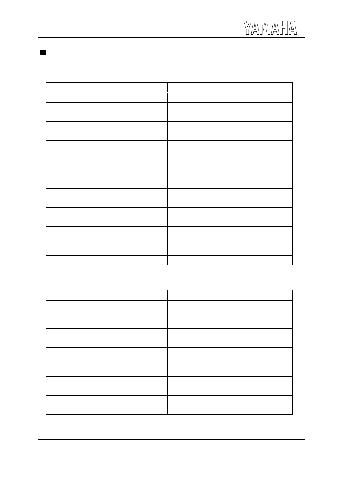
PIN DESCRIPTION
1. PCI Bus Interface (52-pin)
name I/O Type Size function
PCICLK I P PCI Clock
RST# I P Reset
AD[31:0] IO Ptr Address / Data
C/BE[3:0]# IO Ptr Command / Byte Enable
PAR IO Ptr Parity
FRAME# IO Pstr Frame
IRDY# IO Pstr Initiator Ready
TRDY# IO Pstr Target Ready
STOP# IO Pstr Stop
IDSEL I P ID Select
DEVSEL# IO Pstr Device Select
REQA# O P PCI Request
GNTA# I P PCI Grant
PCREQ# O Ptr PC/PCI Request
PCGNT# I Ptr PC/PCI Grant
PERR# IO Pstr Parity Error
SERR# O Pod System Error
INTA# O Pod Interrupt signal output for PCI bus
2. Legacy Device Interface (16-pin)
name I/O type size function
IRQ5 O Ttr 12mA Interrupt5 of Legacy Audio
It is directly connected to the interrupt signal of
System I/O chip.
IRQ7 O Ttr 12mA Interrupt7 of Legacy Audio
IRQ9 O Ttr 12mA Interrupt9 of Legacy Audio
IRQ10 O Ttr 12mA Interrupt10 of Legacy Audio
IRQ11 O Ttr 12mA Interrupt11 of Legacy Audio.
GP[3:0] I A - Game Port
GP[7:4] I Tup - Game Port
GREF I A - Reference for Game Port
RXD I Tup - MIDI Data Receive
TXD O T 3mA MIDI Data Transfer
-3-
January 14, 1999
Page 4
YMF740C
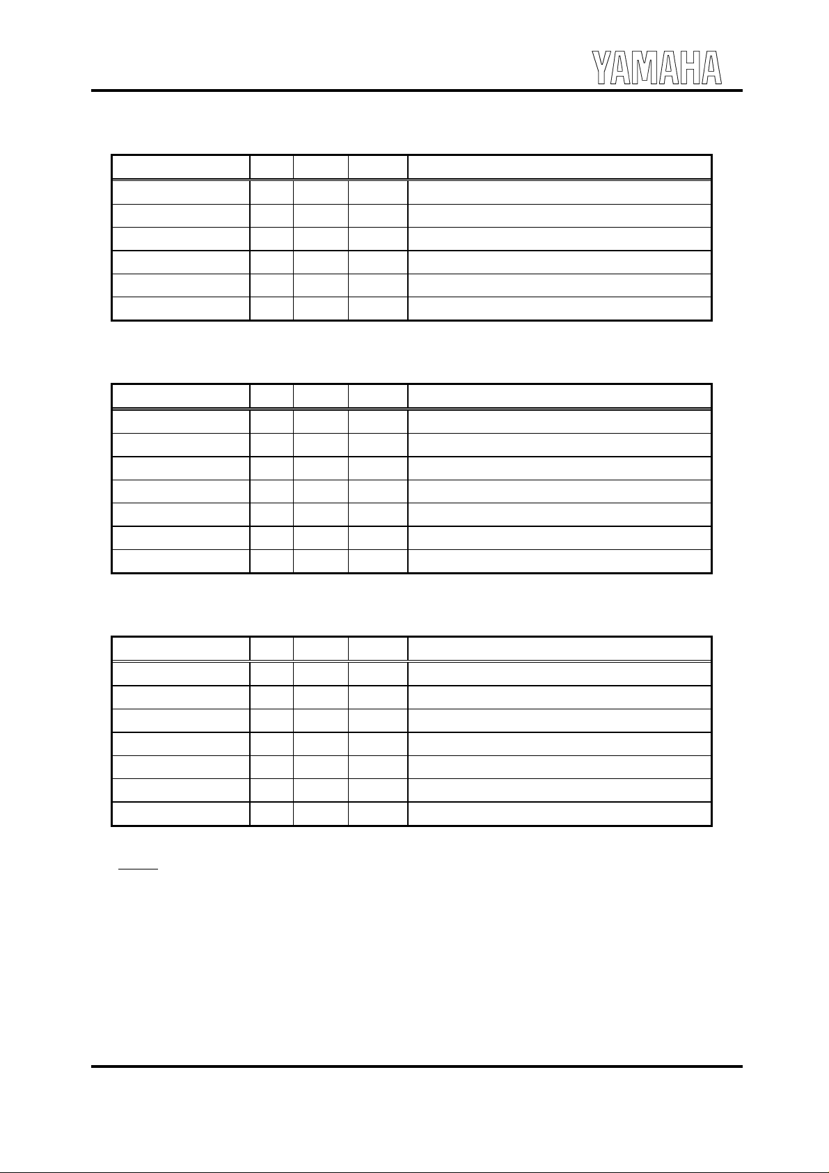
3. AC’97 Interface (6-pin)
name I/O Type Size function
CRST# O T 6mA Reset signal for AC’97
CMCLK O C - Master Clock of AC link (24.576MHz) and
CBCLK I T - AC-link: Bit Clock for AC’97 audio data
CSDO O T 6mA AC-link: AC‘97 Serial audio output data
CSDI I T - AC-link: AC’97 Serial audio input data
CSYNC O T 6mA AC-link: Synchronized signal
4. Miscellaneous (14-pin)
name I/O type size function
VOLUP# I Tup - Hardware Volume (Up)
VOLDW# I Tup - Hardware Volume (Down)
XI24 I C - 24.576 MHz Crystal
XO24 O C 2mA 24.576 MHz Crystal
TEST[7:4,2:0]# I Tup - Test pins (Do not connect externally)
TEST3# IO Tup 3mA Test pin (Connect to ground)
LOOPF[1:0] - - - Capacitor of PLL
5. Power Supply (39-pin)
name I/O type size function
PVDD[5:0] - - - Power supply for PCI Bus Interface (+5.0)
PVSS[14:0] - - - Ground for PCI Bus Interface
LVDD - - - Power supply for PLL Filter (+3.3)
LVSS - - - Ground for PLL Filter
VDD3[3:0] - - - Power supply (+3.3V)
VDD5[3:0] - - - Power supply (+5.0V)
VSS[7:0] - - - Ground
TYPE
T : TTL A : Analog Ptr : Tri-State PCI
Ttr : Tri-State TTL C : CMOS Pstr : Sustained Tri-Sate PCI
Tup : Pull up (Max. 300kohm) TTL P : PCI Pod : Open Drain PCI
Note) All pins except the above pins are NC (No Connection) pins. Do not connect externally.
-4-
January 14, 1999
Page 5
YMF740C
BLOCK DIAGRAM
PC-PCI
PCI Bus
Interface
Legacy Audio
SB Pro
FM
MPU401
Joystick
BUS Master
DMA Controller
Memory
Rate Converter
/ Mixer
AC'97
Interface
PCI Audio
XG Synthesizer
Direct Sound Acc.
Wave In/Out
-5-
January 14, 1999
Page 6
YMF740C
SYSTEM DIAGRAM
DirectX
Application
DLS
Appllication
VxD
DirectSound
Win32API
Soft
Effect
HAL
DirectSound
VxD for PCI Audio
Win16API
MMSystem
Device
MidiOut
Device
WaveOut
Device
WaveIn
MidiIn
Device
Device
MidiOut
DRV for PCI Audio
Engine
XG/DLS
DRV for Legacy
I/O Traps
PCI Audio
DS-1L Slot Manager (Up to 32-sound)
YMF740C(DS-1L)
VxD for Legacy
MPU401
VM
DOS
I/O Traps
Msjstck.drv
FM SB Pro
Vjoyd.vxd
Joystick
January 14, 1999
-6-
Page 7
YMF740C
FUNCTION OVERVIEW
1. PCI INTERFACE
DS-1L supports the PCI bus interface and complies to PCI revision 2.1.
1-1. PCI Bus Command
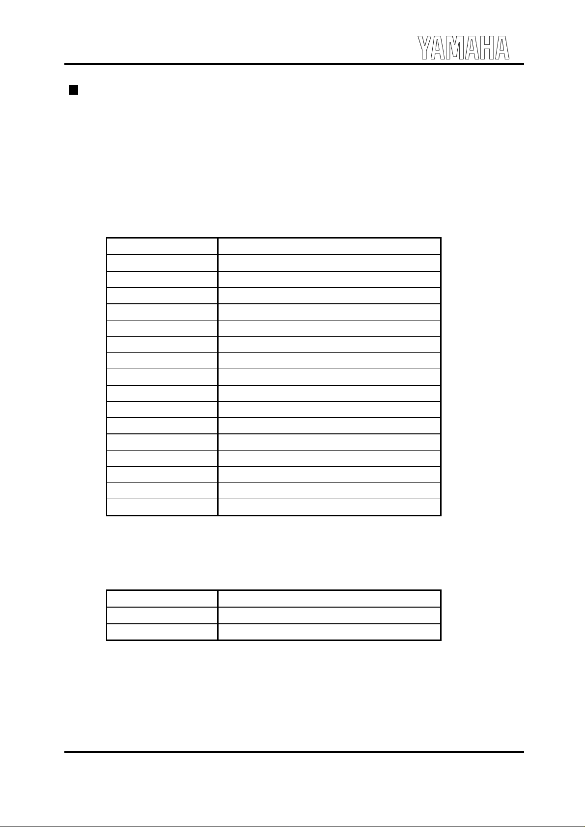
DS-1L supports the following PCI Bus commands.
1-1-1. Target Device Mode
C/BE[3:0]# Command
0000Interrupt Acknowledge (not support)
0001Special Cycle (not support)
0010I/O Read
0011I/O Write
0100reserved
0101reserved
0110Memory Read
0111Memory Write
1000reserved
1001reserved
1010Configuration Read
1011Configuration Write
1100Memory Read Multiple (not support)
1101Dual Address Cycle (not support)
1110Memory Read Line (not support)
1111Memory Write and Invalidate (not support)
DS-1L does not assert DEVSEL# when accessed with commands that are indicated as (not supported) or
reserved.
1-1-2. Master Device Mode
C/BE[3:0]# Command
0110Memory Read
0111Memory Write
When DS-1L becomes a Master Device, it generates only memory write and read cycle commands.
-7-
January 14, 1999
Page 8
YMF740C
1-2. PCI Configuration Register
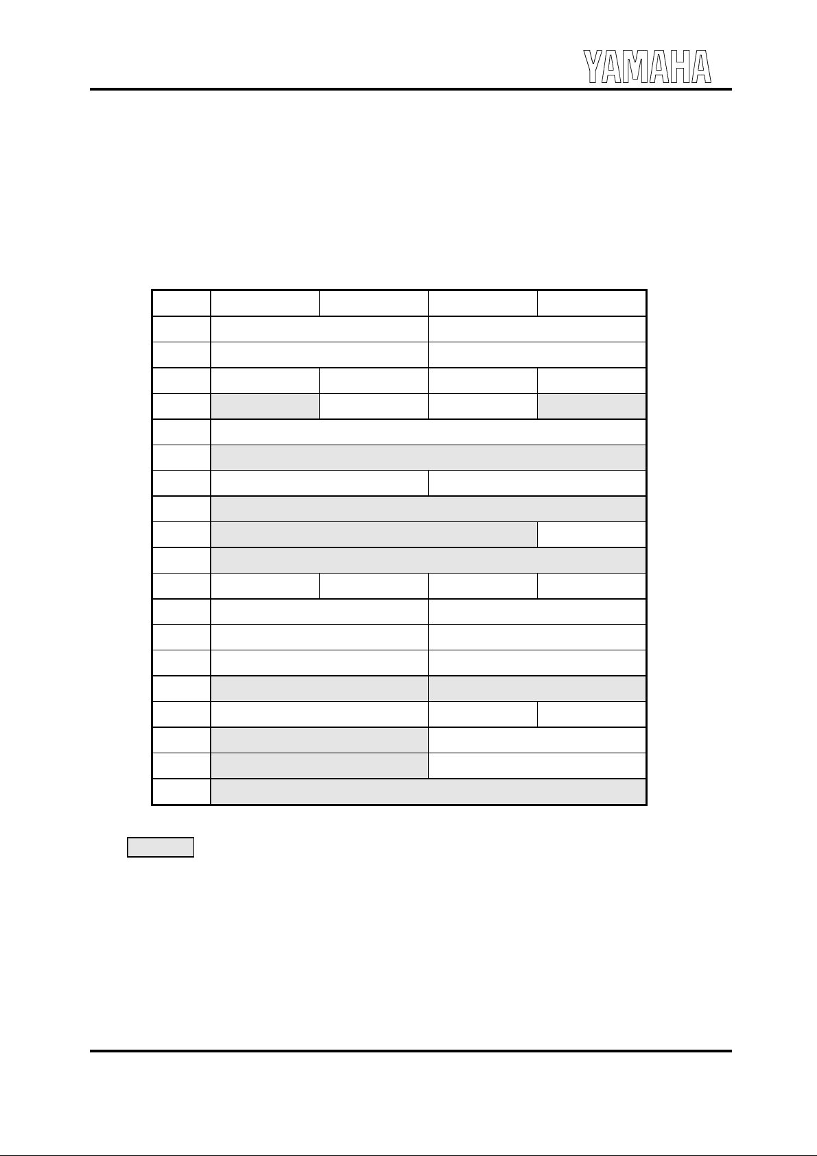
In addition to the Configuration Register defined by PCI Revision 2.1, DS-1L provides proprietary PCI
Configuration Registers in order to control legacy audio functio n, such as FM Synthesizer, Sound Blaster Pro,
MPU401 and Joystick. These additional registers are configured by BIOS or the configuration software
from YAMAHA Corporation.
The following shows the overview of the PCI Configuration Register.
Offset b[31..24] b[23..16] b[15..8] b[7..0]
00-03h Device ID Vendor ID
04-07h Status Command
08-0Bh Base Class Code Sub Class Code Programming IF Revision ID
0C-0Fh Reserved Header Type Latency Timer Reserved
10-13h PCI Audio Memory Base Addres s
14-2Bh Reserved
2C-2Fh Subsystem ID Subsystem Vendor ID
30-33h Reserved
34-37h Reserved Cap Pointer
38-3Bh Reserved
3C-3Fh Maximum Latency Minimum Grant Interrupt Pin Interrupt Line
40-43h Extended Legacy Audio Control Legacy Audio Control
44-47h Subsystem ID Write Subsystem Vendor ID Write
48-4Bh DS-1L Power Control DS-1L Control
4C-4Fh Reserved Reserved
50-53h Power Management Capabilities Next Item Pointer Capability ID
54-57h Reserved Power Management Control / Status
58-5Bh Reserved ACPI Mode
5C-FFh Reserved
Reserved registers are hardwired to “0”. All data written to these registers are discarded. The values
read from these registers are all zero.
DS-1L can be accessed by using any bus width, 8-bit, 16-bit or 32-bit.
-8-
January 14, 1999
Page 9
YMF740C
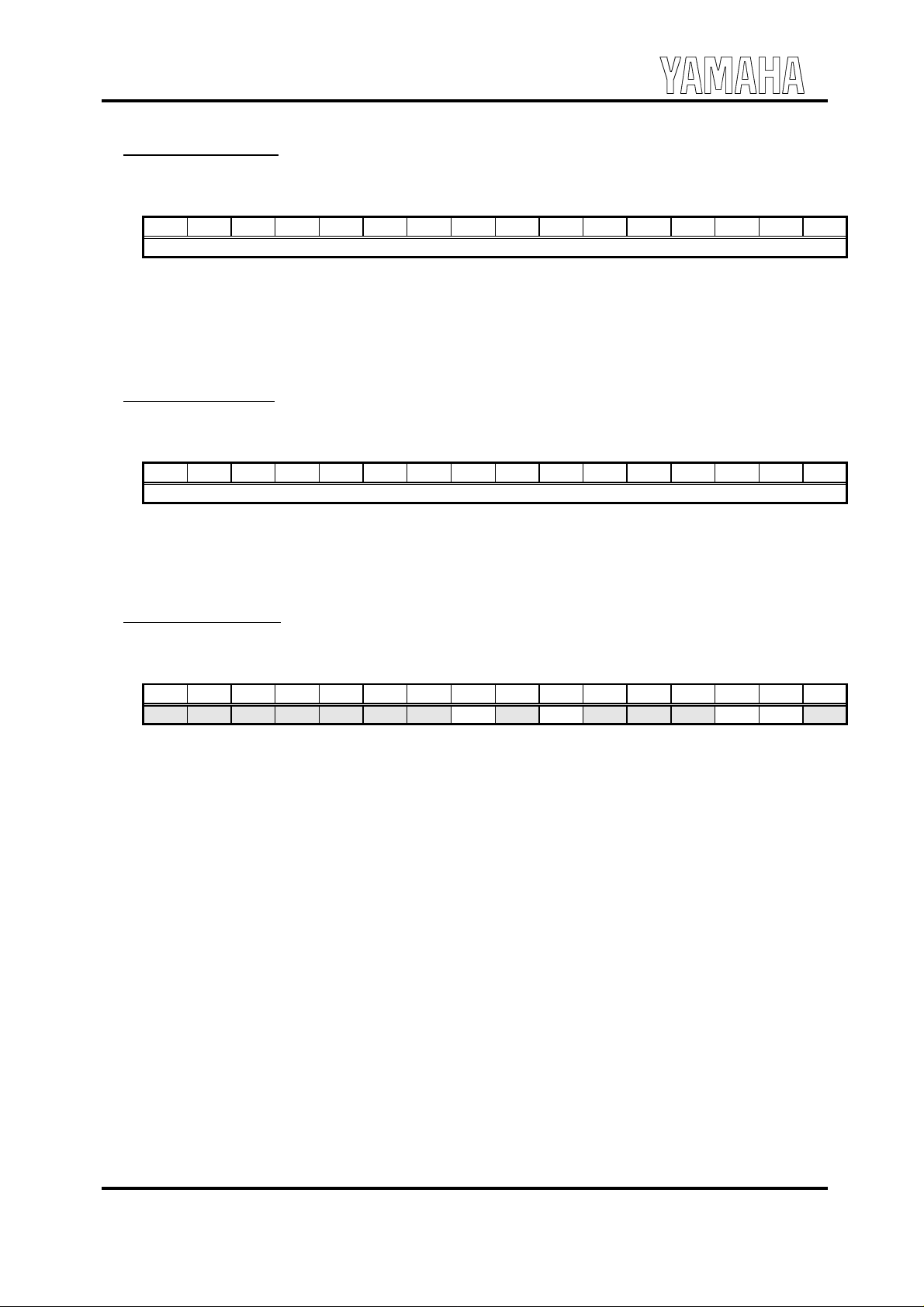
00 - 01h: Vendor ID
Read Only
Default: 1073h
Access Bus Width: 8, 16, 32-bit
b15 b14 b13 b12 b11 b10 b9 b8 b7 b6 b5 b4 b3 b2 b1 b0
Vendor ID
b[15:0]........Vendor ID
This register contains the YAMAHA Vendor ID registered in Revision 2.1. This register is hardwired to
1073h.
02 - 03h: Device ID
Read Only
Default: 000Ch
Access Bus Width: 8, 16, 32-bit
b15 b14 b13 b12 b11 b10 b9 b8 b7 b6 b5 b4 b3 b2 b1 b0
Device ID
b[15:0]........Device ID
This register contains the Device ID of DS-1L. This register is hardwired to 000Ch.
04 - 05h: Command
Read / Write
Default: 0000h
Access Bus Width: 8, 16, 32-bit
b15 b14 b13 b12 b11 b10 b9 b8 b7 b6 b5 b4 b3 b2 b1 b0
- - - - - - - SER - PER - - - BME MS -
b1................MS: Memory Space
This bit enables DS-1L to response to Memory Space Access.
“0”: DS-1L ignores Memory Space Access. (default)
“1”: DS-1L responds to Memory Space Access.
b2................BME: Bus Master Enable
This bit enables DS-1L to act as a master device on the PCI bus.
“0”: Do not set DS-1L to be the master device. (default)
“1”: Set DS-1L to be the master device.
b6................PER: Parity Error Response
This bit enables DS-1L responses to Parity Error.
“0”: DS-1L ignores all parity errors.
“1”: DS-1L performs error operation when DS-1L detects a parity error.
-9-
January 14, 1999
Page 10
YMF740C
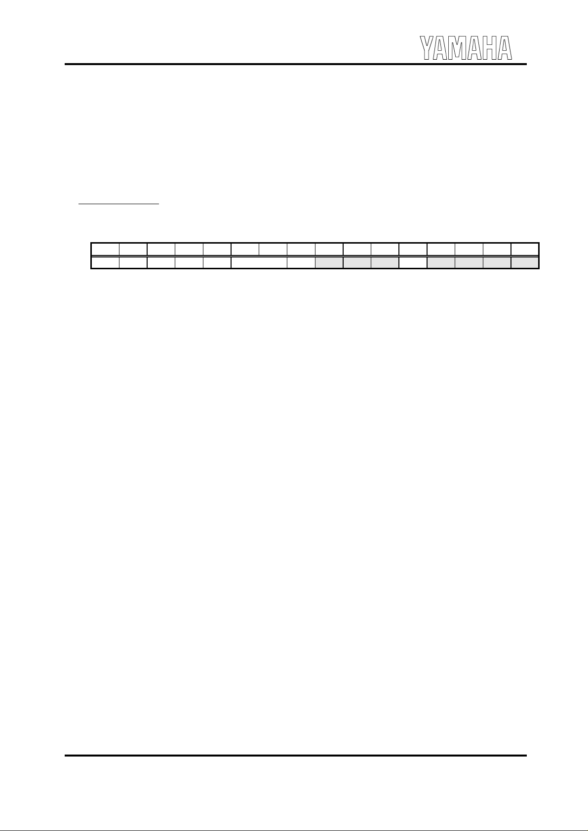
b8................SER: SERR# Enable
This bit enables DS-1L to drive SERR#.
“0”: Do not drive SERR# . (default)
“1”: Drives SERR# when DS-1L detects an Address Parity Error on normal target cycle or a Data Parity
Error on special cycle.
06 - 07h: Status
Read / Write Clear
Default: 0210h
Access Bus Width: 8, 16, 32-bit
b15 b14 b13 b12 b11 b10 b9 b8 b7 b6 b5 b4 b3 b2 b1 b0
DPE SSE RMA RTA STA DEVT DPD - - - CAP - - - -
b4................CAP: Capability (Read Only)
This bit indicates that DS-1L supports the capability register. This bit is read only. When 58-59h :
ACPI Mode register, ACPI bit is “0”, the bit is “1”. When ACPI bit is “1”, the bit is “0”.
b8................DPD: Data Parity Error Detected
This bit indicates that DS-1L detects a Data Parity Error during a PCI master cycle.
b[10:9] ........DEVT: DEVSEL Timing
This bit indicates that the decoding speed of DS-1L is Medium.
b11..............STA: Signaled Target Abort
This bit indicates that DS-1L terminates a transaction with Target Abort during a target cycle.
b12..............RTA: Received Target Abort
This bit indicates that a transaction is terminated with Target Abort while DS-1L is in the master memory
cycle.
b13..............RMA: Received Master Abort
This bit indicates that a transaction is terminated with Master Abort while DS-1L is in the master memory
cycle.
b14..............SSE: Signaled System Error
This bit indicates that DS-1L asserts SERR#.
b15..............DPE: Detected Parity Error
This bit indicates that DS-1L detects Address Parity Error or Data Parity Error during a transaction.
January 14, 1999
-10-
Page 11
YMF740C
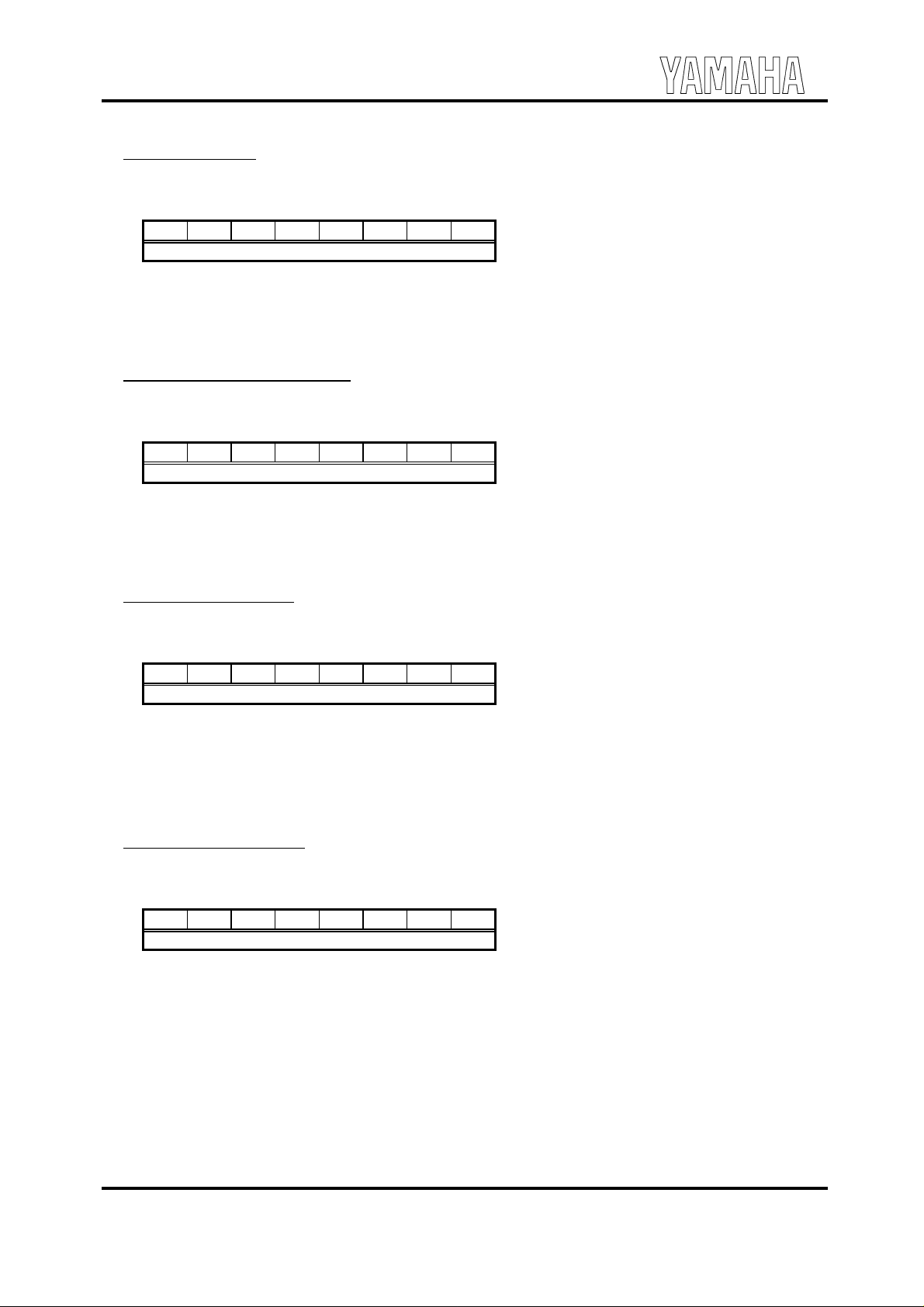
08h: Revision ID
Read Only
Default: 03h
Access Bus Width: 8, 16, 32-bit
b7 b6 b5 b4 b3 b2 b1 b0
Revision ID
b[7:0]..........Revision ID
This register conta i ns the revision number of DS-1L. This register is hardwired to 03h.
09h: Programming Interface
Read Only
Default: 00h
Access Bus Width: 8, 16, 32-bit
b7 b6 b5 b4 b3 b2 b1 b0
Programming Interf ace
b[7:0]..........Programming Interface
This register indicates the programming interface of DS-1L. This register is hardwired to 00h.
0Ah: Sub-class Code
Read Only
Default: 01h
Access Bus Width: 8, 16, 32-bit
b7 b6 b5 b4 b3 b2 b1 b0
Sub-class Code
b[7:0]..........Sub-class Code
This register indicates the sub-class of DS-1L. This register is hardwired to 01h. DS-1L belongs to the
Audio Sub-class.
0Bh: Base Class Code
Read Only
Default: 04h
Access Bus Width: 8, 16, 32-bit
b7 b6 b5 b4 b3 b2 b1 b0
Base Class Code
b[7:0]..........Base Class Code
This register indicates the base class of DS-1L. This register is hardwired to 04h. DS-1L belongs to
the Multimedia Base Class.
January 14, 1999
-11-
Page 12
YMF740C
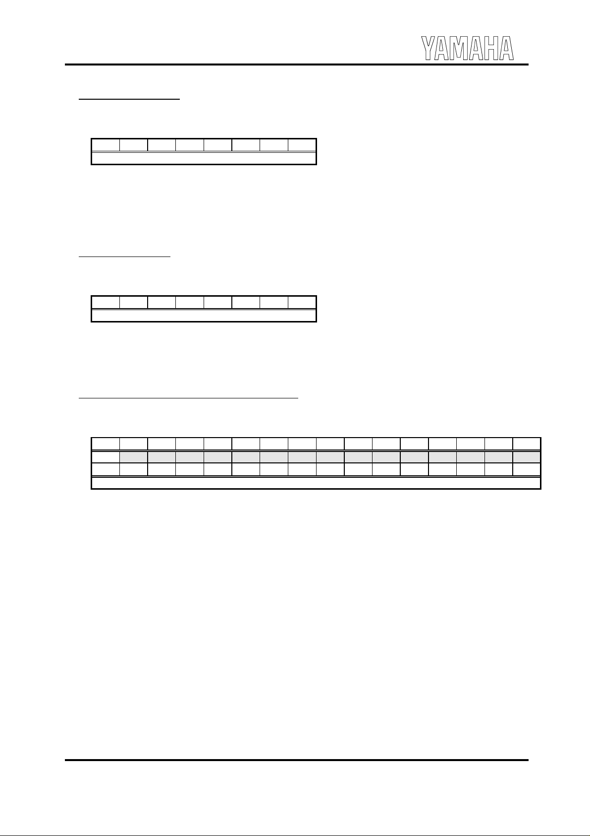
0Dh: Latency Timer
Read / Write
Default: 00h
Access Bus Width: 8, 16, 32-bit
b7 b6 b5 b4 b3 b2 b1 b0
Latency Timer
b[7:0]..........Latency Timer
When DS-1L becomes a Bus Master device, this register indicates the initial value of the Master Latency
Timer.
0Eh: Header Type
Read Only
Default: 00h
Access Bus Width: 8, 16, 32-bit
b7 b6 b5 b4 b3 b2 b1 b0
Header Type
b[7:0]..........Header Type
This register indicates the device type of DS-1L. This is hardwired to 00h.
10 - 13h: PCI Audio Memory Base Address
Read / Write
Default: 00000000h
Access Bus Width: 8, 16, 32-bit
b15 b14 b13 b12 b11 b10 b9 b8 b7 b6 b5 b4 b3 b2 b1 b0
MBA
b31 b30 b29 b28 b27 b26 b25 b24 b23 b22 b21 b20 b19 b18 b17 b16
b[31:15]......MBA: Memory Base Address
This register indicates the physical Memory Base address of the PCI Audio registers in DS-1L. T he base
address can be located anywhere in the 32-bit address space. Data in the DS-1L register is not
prefetchable.
DS-1L needs 32768-bytes of memory address space.
- - - - - - - - - - - - - - -
MBA (higher)
-12-
January 14, 1999
Page 13
YMF740C
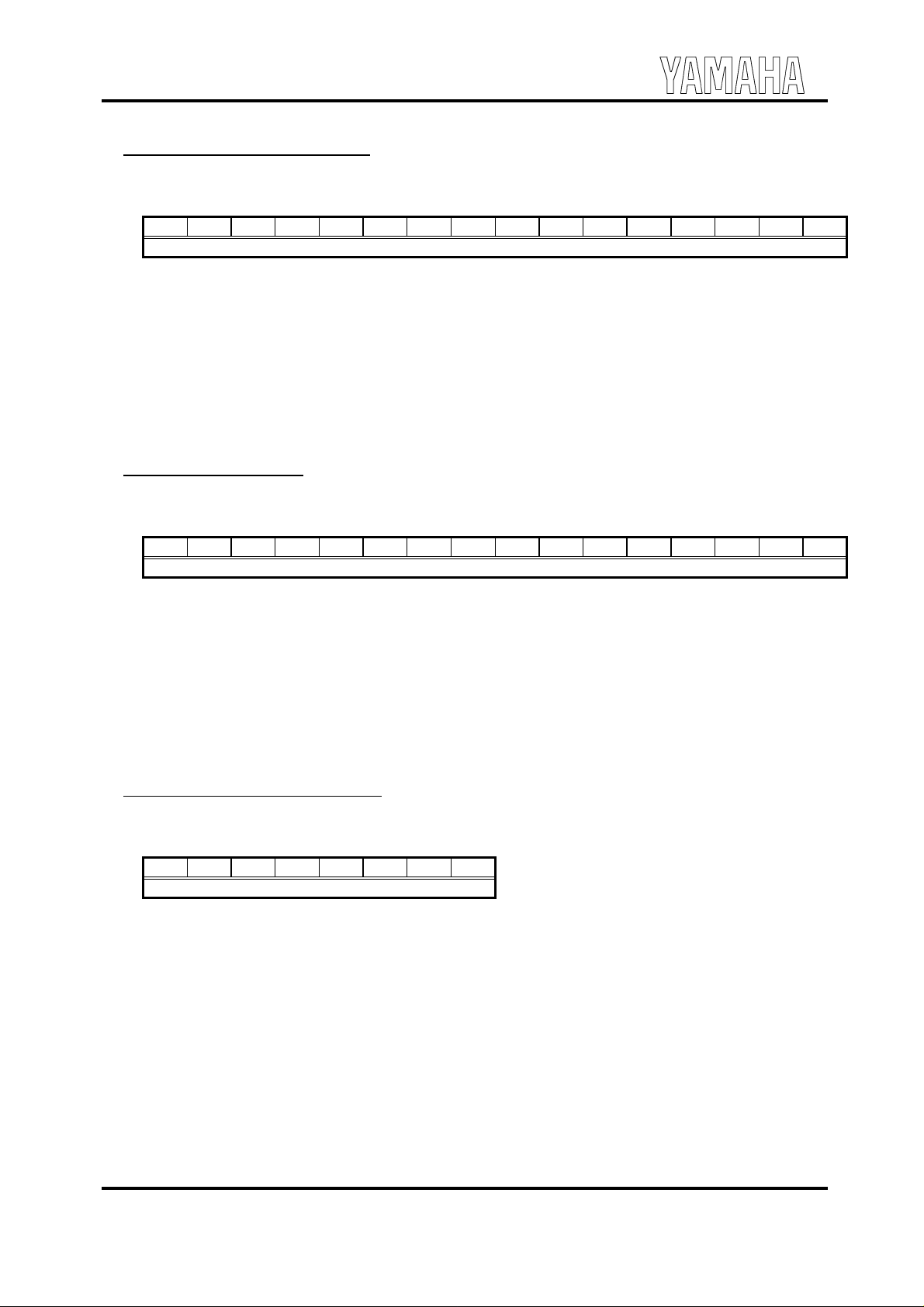
2C-2Dh: Subsystem Vendor ID
Read Only
Default: 1073h
Access Bus Width: 8, 16, 32-bit
b15 b14 b13 b12 b11 b10 b9 b8 b7 b6 b5 b4 b3 b2 b1 b0
Subsystem Vendor ID
b[15:0]........Subsystem Vendor ID
This register contains the Subsystem Vendor ID. In genera l, this ID is used to distinguish adapters or
systems made by different IHVs using the same chip by the same vendor. This register is read only. To
write the IHV’s Vendor ID, use 44-45h (Subsystem Vendor ID Write Register).
The default value is the YAMAHA's Vendor ID, 1073h. IHVs must change this ID to their Vendor ID in
the BIOS POST routine.
2E-2Fh: Subsystem ID
Read Only
Default: 000Ch
Access Bus Width: 8, 16, 32-bit
b15 b14 b13 b12 b11 b10 b9 b8 b7 b6 b5 b4 b3 b2 b1 b0
Subsystem ID
b[15:0]........Subsystem ID
This register contains the Subsystem ID. In general, this ID is used to distinguish adapters or systems
made by different IHVs using the same chip by the same vendor. This register is read only. To write
the IHV's Device ID, use 46-47h (Subsystem ID Write Register).
The default value is the YAMAHA's Device ID, 000Ch. IHVs must change this ID to their ID in the
BIOS POST routine.
34h: Capability Register Pointer
Read Only
Default: 50h
Access Bus Width: 8, 16, 32-bit
b7 b6 b5 b4 b3 b2 b1 b0
Capability Register Pointer
b[7:0]..........Capability Register Pointer
This register indicates the offset address of the Capabilities register in the PCI Configuration register
when 58-59h: ACPI Mode register, ACPI bit is “0”. DS-1L provides PCI Bus Power Management
registers as the capabilities. The Power Management registers are mapped to 50h - 57h in the PCI
Configuration register, and this register indicates “50h”.
When ACPI bit is “1”, this register indicates “00h”.
-13-
January 14, 1999
Page 14
YMF740C
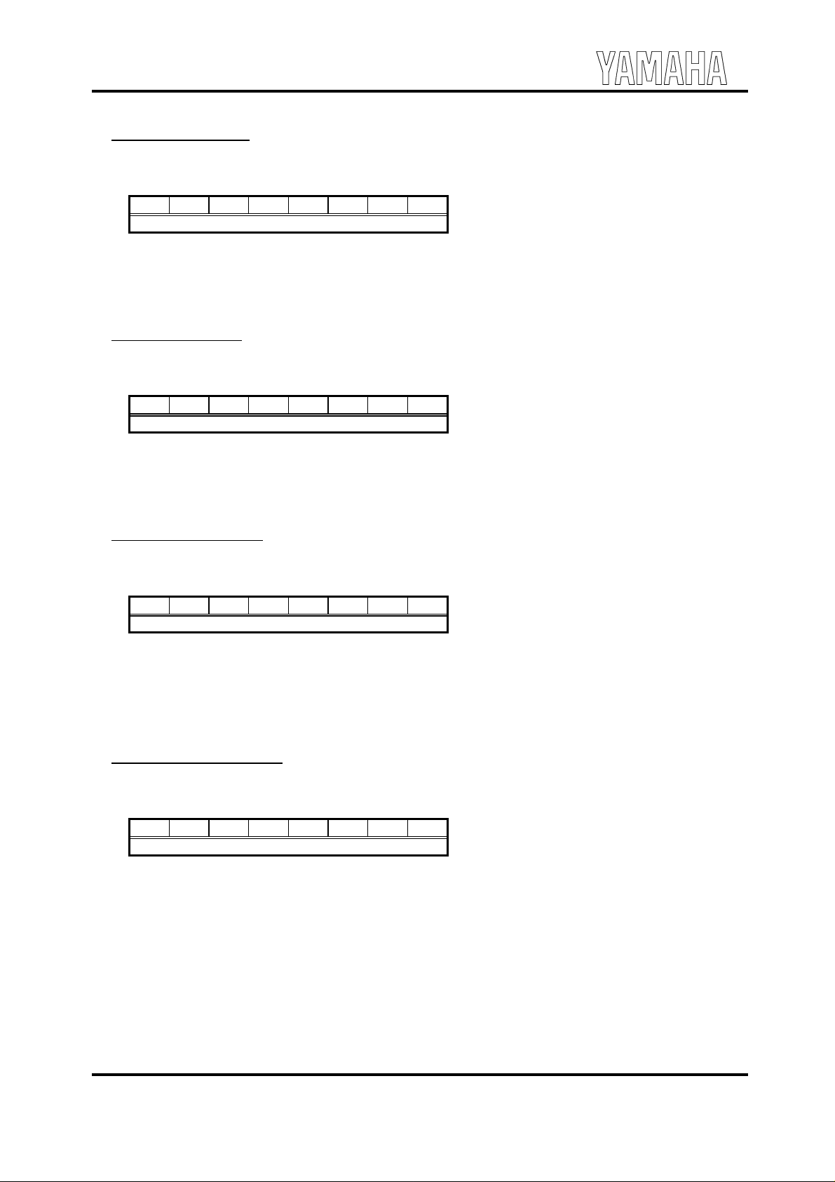
3Ch: Interrupt Line
Read / Write
Default: 00h
Access Bus Width: 8, 16, 32-bit
b7 b6 b5 b4 b3 b2 b1 b0
Interrupt Line
b[7:0]..........Interrupt Line
This register indicates the interrupt channel that INTA# is assigned to.
3Dh: Interrupt Pin
Read Only
Default: 01h
Access Bus Width: 8, 16, 32-bit
b7 b6 b5 b4 b3 b2 b1 b0
Interrupt Pin
b[7:0]..........Interrupt Pin
DS-1L supports INTA# only. This register is hardwired to 01h.
3Eh: Minimum Grant
Read Only
Default: 05h
Access Bus Width: 8, 16, 32-bit
b7 b6 b5 b4 b3 b2 b1 b0
Minimum Grant
b[7:0]..........Minimum Grant
This register indicates the length of the burst period required by DS-1L.
This register is hardwired to 05h.
3Fh: Maximum Latency
Read Only
Default: 19h
Access Bus Width: 8, 16, 32-bit
b7 b6 b5 b4 b3 b2 b1 b0
Maximum Latency
b[7:0]..........Maximum Latency
This register indicates how often DS-1L generates the Bus Master Request.
This register is hardwired to 19h.
-14-
January 14, 1999
Page 15

YMF740C
40 - 41h: Legacy Audio Control
Read / Write
Default: 907Fh
Access Bus Width: 8, 16, 32-bit
b15 b14 b13 b12 b11 b10 b9 b8 b7 b6 b5 b4 b3 b2 b1 b0
”0”
LAD
b0................SBEN: Sound Blaster Enable
This bit enables the mapping of the Sound Blaster Pro block in the I/O space specified by the SBIO bits,
when LAD is set to “0”. T he FM Synthesizer registers can be accessed via SB I/O space, while the SB
block is enabled, even if FMEN is set to “0”.
“0”: Disable the mapping of the SB block to the I/O space
“1”: Enable the mapping of the SB block to the I/O space (default)
b1................FMEN: FM Synthesizer Enable
This bit enables the mapping of the FM Synthesizer block in the I/O space specified by the FMIO bits,
when LAD is set to “0”. FM Synthesizer registers can be accessed via SB I/O space, while the SB block
is enabled, even if FMEN is set to “0”.
“0”: Disable the mapping of the FM Synthesizer block to the FMIO space
“1”: Enable the mapping of the FM Synthesizer block to the FMIO space (default)
After setting FMEN to “1”, about 100 msec is necessary before accessing these I/O space.
MPUIRQ SBIRQ SDMA I/O MIEN MEN GPEN FMEN SBEN
b2................GPEN: Gameport Enable
This bit enables the mapping of the Joystick block in the I/O space specified by the JSIO bits, when LAD
is set to “0”.
“0”: Disable the mapping of the Joystick block
“1”: Enable the mapping of the Joystick block (default)
b3................MEN: MPU401 Enable
This bit enables the mapping of the MPU401 block in the I/O space specified by the MPUIO bits, when
LAD is set to “0”.
“0”: Disable the mapping of the MPU401 block
“1”: Enable the mapping of the MPU401 block (default)
b4................MIEN: MPU401 IRQ Enable
This bit enables the interrupt service of MPU401, when LAD is set to “0” and MEN is set to “1”.
MPU401 generates an interrupt signal when it receives any kind of MIDI data from the RXD pin.
“0”: The MPU401 block can not use the interrupt service.
“1”: The MPU401 block can use interrupt signals determined by the MPUIRQ bits. (default)
b5................I/O: I/O Address Aliasing Control
This bit selects the number of bits to decode for the I/O address of each block.
“0”: 16-bit address decode
“1”: 10-bit address decode (default)
-15-
January 14, 1999
Page 16

YMF740C
b[7:6]..........SDMA: Sound Blaster DMA-8 Channel Select
These bits select the DMA channel for the Sound Blaster Pro block.
“0”: DMA ch0
“1”: DMA ch1 (default)
“2”: reserved
“3”: DMA ch3
b[10:8]........SBIRQ: Sound Blaster IRQ Channel Select
These bits select the interrupt channel for the Sound Blaster Pro block.
“0”: IRQ5 (default)
“1”: IRQ7
“2”: IRQ9
“3”: IRQ10
“4”: IRQ11
“5” - “7”: reserved.
b[13:11]......MPUIRQ: MPU401 IRQ Channel Select
When MIEN is set to “1”, these bits select the interrupt channel for the MPU401 block.
“0”: IRQ5
“1”: IRQ7
“2”: IRQ9 (default)
“3”: IRQ10
“4”: IRQ11
“5” - “7”: reserved
Same interrupt channels can be assigned to SBIRQ and MPUIRQ.
b14..............Reserved Bit
Hardwire to “0”.
b15..............LAD: Legacy Audio Disable
This bit disables the Legacy Audio block.
“0”: Enables the Legacy Audio block
“1”: Disables the Legacy Audio block (default)
When this bit is set to “1”, DS-1L does not respond to the I/O Target transaction for legacy I/O address on
the PCI bus.
-16-
January 14, 1999
Page 17

YMF740C
42 - 43h: Extended Legacy Audio Control
Read / Write
Default: 0000h
Access Bus Width: 8, 16, 32-bit
b15 b14 b13 b12 b11 b10 b9 b8 b7 b6 b5 b4 b3 b2 b1 b0
IMOD SBVER SMOD - - MAIM JSIO MPUIO SBIO FMIO
b[1:0]..........FMIO: FM I/O Address allocation
These bits determine the base I/O address for the of the FM Synthesizer block (FMBase).
FM Synthesizer block uses 4 bytes in the I/O address space.
“0”: 388h (default)
“1”: 398h
“2”: 3A0h
“3”: 3A8h
b[3:2]..........SBIO: SB I/O Address allocation
These bits determine the base I/O address for the Sound Blaster Pro block (SBBase). This block uses 16
bytes in the I/O address space.
“0”: 220h (default)
“1”: 240h
“2”: 260h
“3”: 280h
b[5:4]..........MPUIO: MPU I/O Address allocation
These bits determine the base I/O address for the MPU401 block (MPUBase). T his block uses 2 bytes
in the I/O address space.
“0”: 330h (default)
“1”: 300h
“2”: 332h
“3”: 334h
b[7:6]..........JSIO: Joystick I/O Address allocation
These bits determine the base I/O address for the Joystick block (JSBase). This blo ck uses 1 byte in the
I/O address space.
“0”: 201h (default)
“1”: 202h
“2”: 204h
“3”: 205h
b8................MAIM: MPU401 Acknowledge Interrupt Mask
This bit determine whether interrupt is asserted when the acknowledge, which is occurred by changing
MPU401 mode form default to UART, is returned.
“0”: Interrupt is asserted when the acknowledge is returned. (default)
“1”: Interrupt is masked when the acknowledge is returned.
-17-
January 14, 1999
Page 18
YMF740C
b[12:11]......SMOD: SB DMA mode
These bits determine the protocol to achieve the DMAC(8237) function on the PCI bus.
“0”: PC/PCI (default)
“1” - “3”: reserved
b[14:13]......SBVER: SB Version Select
These bits set the version of the SB Pro DSP . The value set in these bits is returned b y sending the E1h
DSP command.
“0”: ver 3.01 (default)
“1”: ver 2.01
“2”: ver 1.05
“3”: reserved
b15..............IMOD: Legacy IRQ mode
DS-1L supports 2 types of interrupt protocols: PCI interrupt (INTA#) and Legacy interrupt (IRQs). The
interrupt protocol is selected by IMOD as follows. T he interrupt channels for IRQs are determined by
SBIRQ and MPUIRQ. Only one protocol can be used at once.
“0”: Legacy interrupt (IRQs) (default)
“1”: PCI interrupt (INTA#)
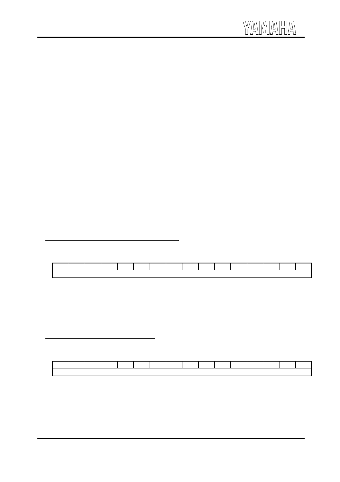
44-45h: Subsystem Vendor ID Write Register
Read / Write
Default: 1073h
Access Bus Width: 16-bit
b15 b14 b13 b12 b11 b10 b9 b8 b7 b6 b5 b4 b3 b2 b1 b0
Subsystem Vendor ID Write
b[15:0]........Subsystem Vendor ID Write Register
This register sets the Subsystem Vendor ID that is read from 2C-2Dh (Subsystem Vendor ID register).
The default value is the YAMAHA Vendor ID, 1073h. IHVs must change this ID to their Vendor ID in
the BIOS POST routine.
46-47h: Subsystem ID Write Register
Read / Write
Default: 000Ch
Access Bus Width: 16-bit
b15 b14 b13 b12 b11 b10 b9 b8 b7 b6 b5 b4 b3 b2 b1 b0
Subsystem ID Write
b[15:0]........Subsystem ID Write Register
This register sets the Subsystem ID that is read from 2E-2Fh (Subsystem ID register).
The default value is the DS-1L Device ID, 000Ch. IHVs must change this ID to their ID in the BIOS
POST routine.
-18-
January 14, 1999
Page 19
YMF740C
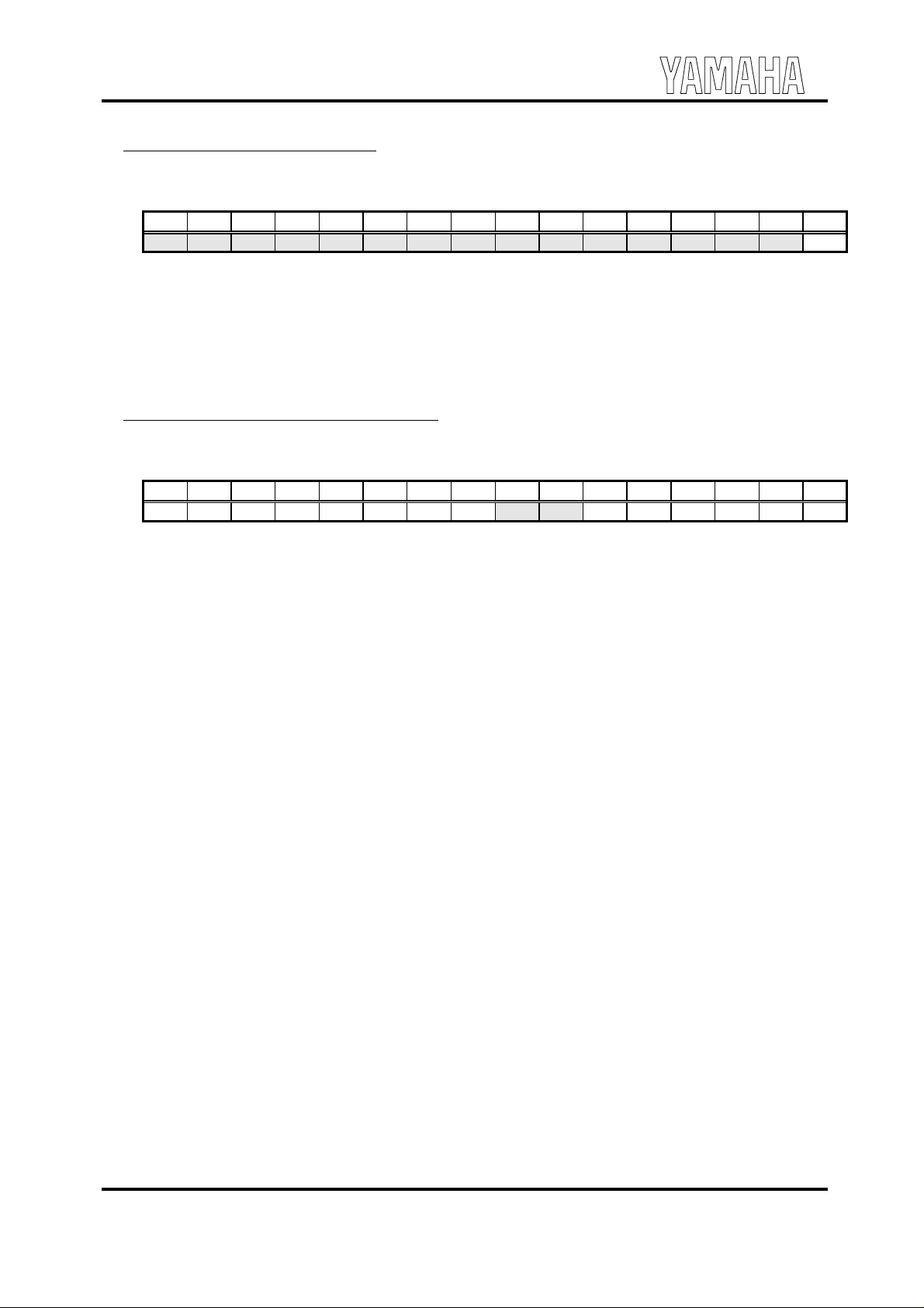
48-49h: DS-1L Control Register
Read / Write
Default: 0001h
Access Bus Width: 8, 16, 32-bit
b15 b14 b13 b12 b11 b10 b9 b8 b7 b6 b5 b4 b3 b2 b1 b0
- - - - - - - - - - - - - - - CRST
b0................CRST: AC’97 Software Reset Signal Control
This bit controls the CRST# signal.
“0”: Inactive (CRST#=High)
“1”: Active (CRST#=Low) (default)
4A-4Bh: DS-1L Power Control Register
Read / Write
Default: 0000h
Access Bus Width: 8, 16, 32-bit
b15 b14 b13 b12 b11 b10 b9 b8 b7 b6 b5 b4 b3 b2 b1 b0
PR7 PR6 PR5 PR4 PR3 PR2 PR1 PR0 - - PSN PSL1 PSL0 DPLL1 DPLL0 DMC
b0................DMC: Disable Master Clock Oscillation
Setting this bit to “1” disables the oscillation of the Master Clock (24.576 MHz).
“0”: Normal (default)
“1”: Disable
b1................DPLL0: Disable PLL0 Clock Oscillation
Setting this bit to “1” disables the oscillation of PLL for the Legacy Audio function.
“0”: Normal (default)
“1”: Disable
b2................DPLL1: Disable PLL1 Clock Oscillation
Setting this bit to “1” disables the oscillation of PLL for the PCI Audio function.
“0”: Normal (default)
“1”: Disable
b3................PSL0: Power Save Legacy Audio Block 0
Setting this bit to “1” stops providing the clock with the Legacy Audio function block 0. This block
includes FM Synthesizer and SB Pro engines.
“0”: Normal (default)
“1”: Power Save
b4................PSL1: Power Save Legacy Audio Block 1
Setting this bit to “1” stops providing the clock with the Legacy Audio function block 1. This block
includes MPU401 and Joystick.
“0”: Normal (default)
“1”: Power Save
January 14, 1999
-19-
Page 20

YMF740C
b5................PSN: Power Save PCI Audio block
Setting this bit to “1” stops pr oviding the clock with the P CI Audio function bl ock. This blo ck includes
PCI Audio, SRC, AC’97 I/F and H/W Vol.
“0”: Normal (default)
“1”: Power Save
b8................PR0: AC’97 Power down Control 0
This bit controls the power state of the ADC and Input Mux in AC’97.
“0”: Normal (default)
“1”: Power down
b9................PR1: AC’97 Power down Control 1
This bit controls the power state of the DAC in AC’97.
“0”: Normal (default)
“1”: Power down
b10..............PR2: AC’97 Power down Control 2
This bit controls the power state of the Analog Mixer (Vref still on) in AC’97. This power state retains
the Reference Voltage of AC’97.
“0”: Normal (default)
“1”: Power down
b11..............PR3: AC’97 Power down Control 3
This bit controls the power state of the Analog Mixer (Vref off) in AC’97. This power state removes
Reference Voltage of AC’97.
“0”: Normal (default)
“1”: Power down
b12..............PR4: AC’97 Power down Control 4
This bit controls the power state of the AC-link in AC’97.
“0”: Normal (default)
“1”: Power down
b13..............PR5: AC’97 Power down Control 5
Setting this bit to “1” disables the internal clock of AC’97. In case AC’97 is used with DS-1L, the
master clock is supplied from DS-1L. Therefore, when the clock of AC’97 is stopped completely, set
both PR5 and PSN bits to “1”.
“0”: Normal (default)
“1”: Disable
b[15:14]......AC’97 Power down Control 6 and 7
These bits control PR6 and PR7 status of the power control register in AC’97.
-20-
January 14, 1999
Page 21
YMF740C
PSL0
Legacy func. 0
Master
(24.576MHz)
DMC DPLL0
PLL0
33.87MHz
PLL1
49.152MHz
DPLL1
PSL1
PSN
FM Synthesizer
SB Pro
Legacy func. 1
MPU401
Joystick
PCI func. 0
AC'97 I/F
H/W V ol.
PCI Audio
SRC
PCI func. 1
PCICLK
(33MHz)
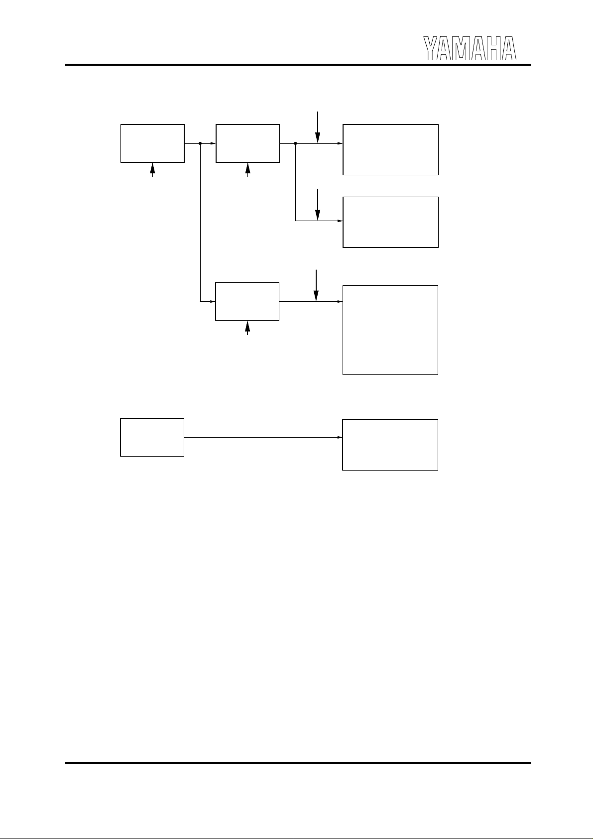
- Set DPLL0, DPLL1, PSL0, PSL1 and PSN bits to “1”, when DMC bit is set to “1”.
- Set PSL0 and PSL1 bits to “1”, when DPLL0 bit is set to “1”.
- Set PSN bit to “1”, when DPLL1 bit is set to “1”.
PCI I/F
PC/PCI
-21-
January 14, 1999
Page 22
YMF740C
50h: Capability ID
Read Only
Default: 01h
Access Bus Width: 8, 16, 32-bit
b7 b6 b5 b4 b3 b2 b1 b0
Capability ID
b[7:0]..........Capability ID: Capability Identifier
This register indicates that the new capability register is for Power Management control. This register is
hardwired to 01h.
51h: Next Item Pointer
Read Only
Default: 00h
Access Bus Width: 8, 16, 32-bit
b7 b6 b5 b4 b3 b2 b1 b0
Next Item Pointer
b[7:0]..........Next Item Pointer
DS-1L does not provide other new capability besides Power Management. This register is hardwired to
00h.
52-53h: Power Management Capabilities
Read Only
Default: 0401h
Access Bus Width: 8, 16, 32-bit
b15 b14 b13 b12 b11 b10 b9 b8 b7 b6 b5 b4 b3 b2 b1 b0
- - - - - D2S - - - - - - - Version
b[2:0]..........Version
These bits contain the revision number of the Power Management Interface Specification. They are
hardwired to 001b.
b10..............D2S: D2 Support
This bit indicates that DS-1L support “D2” of the power state. It is hardwired to “1”.
-22-
January 14, 1999
Page 23
YMF740C
54-55h: Power Management Control / Status
Read / Write
Default: 0000h
Access Bus Width: 8, 16, 32-bit
b15 b14 b13 b12 b11 b10 b9 b8 b7 b6 b5 b4 b3 b2 b1 b0
- - - - - - - - - - - - - - PS
b[1:0]..........PS: Power State
These bits determine the power state of DS-1L. DS-1L supports the following power states:
“0”: D0
“1”: D1 (not supported)
“2”: D2
“3”: D3
When the power state is changed from D3
DS-1L transits to D0 Uninitialized state.
Though the power state of this re gister is changed, the po wer consumption of DS-1 L is not c hanged. To
support low power, Windows driver controls DS-1L Power Control Register.
hot
to D0, DS-1L rese ts the PCI Configuration re gister 00-3Fh.
hot
DS-1L can support the power state of D0, D1, D2 and D3 with ACPI. In this case, set ACPI bit (58-59h:
ACPI Mode Register) to “1” to disable Capabilities of PCI Bus Po wer Management.
58-59h: ACPI Mode
Read / Write
Default: 0000h
Access Bus Width: 8, 16, 32-bit
b15 b14 b13 b12 b11 b10 b9 b8 b7 b6 b5 b4 b3 b2 b1 b0
- - - - - - - - - - - - - - - ACPI
b0................ACPI: ACPI Mode Select
This bit select either PCI Bus Power Management or ACPI Mode for power management of DS-1L.
“0”: PCI Bus Power Management is used. CAP bit (06-07h: Status Register) and Capab ilities Pointer
(34h) are enabled. (default)
“1”: ACPI Mode is used. CAP bit and Capabilities Pointer are hardwired “0”, and disabled.
-23-
January 14, 1999
Page 24
YMF740C
2. ISA Compatible Device
DS-1L contains the following functions to maintain the compatibility with the past ISA Sound Devices.
These devices are considered Legacy devices and the functions are referred to as Legacy Audio.
Legacy Audio is independent from PCI Audio and can be used simultaneously.
The configuration is set in the Legacy Audio Control Register in the PCI Configuration Register space.
Basically, these registers are configured by the BIOS.
Also, logical device IDs are assigned to the devices to support Plug and Play. Yamaha defines the following
logical IDs.
To control the device with the BIOS, the logical device IDs must be defined in the PnP BIOS extended ROM
space. The logical IDs are determined by how it is configured. IDs and configuration are as follows.
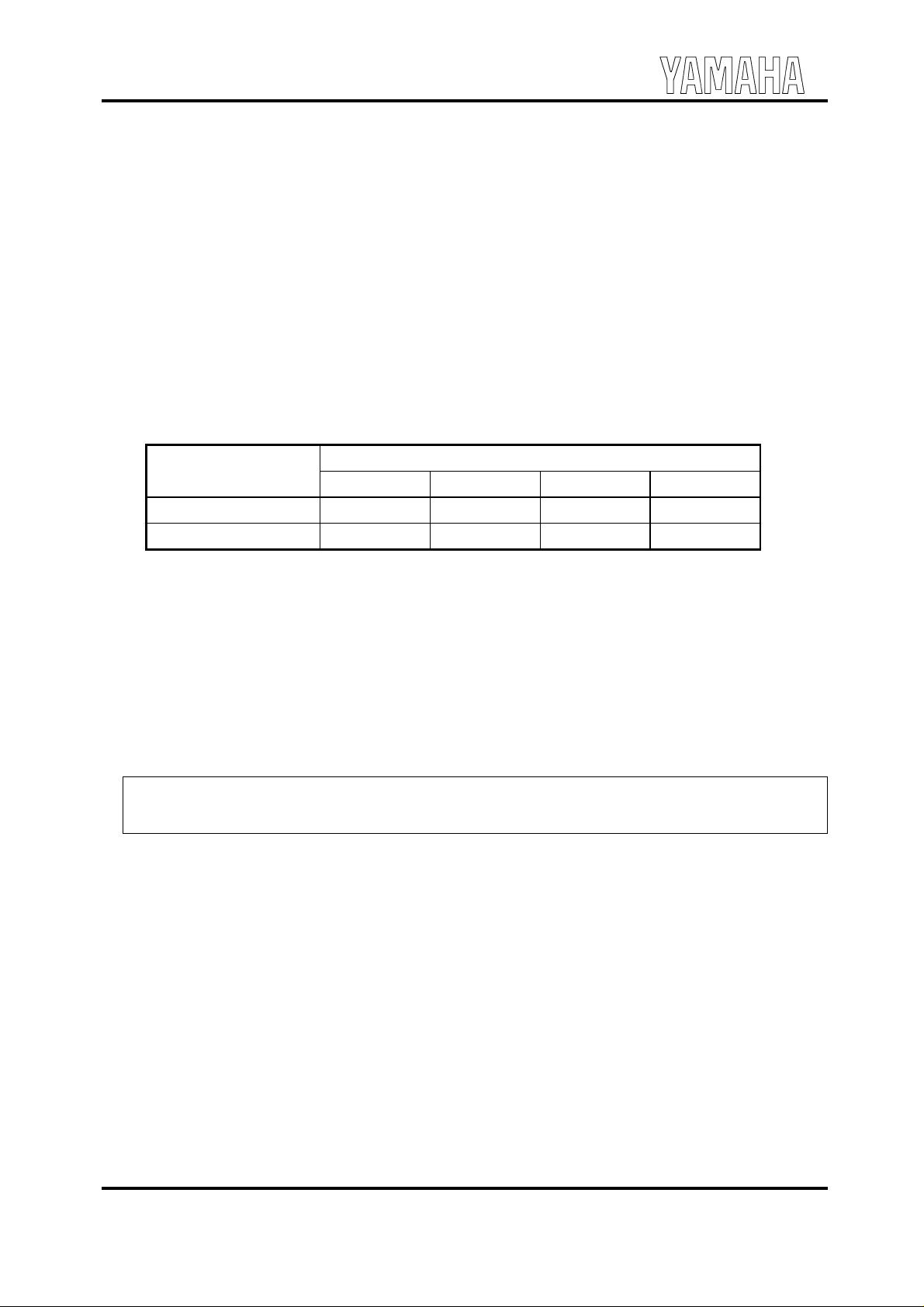
Logical Device ID
YMH0100 O O O
YMH0101 O
* The blocks pertain to the following.
FM: Points to the FM synthesizer mapped to AdLibBase (0x0388).
SB Pro: Points to the Voice Playback section only.
These devices are independent from each other, and can be Enabled/Disabled individually. However, both
AdLib and Sound Blaster must be disabled to disable the internal FM Synthesizer. Disabling just AdLib
only masks the access.
The driver by Yamaha supports only logical device ID, YMH0100. For YMH0101, use the driver provided
by Microsoft.
DS-1L supports PC/PCI protocol to emulate the DMA of SB Pro on the PCI. In addition, DS-1L supports
the old type of interrupts used by ISA.
The PCI-to-ISA bridge needs to support PC/PCI. IRQ is directly connected to the IRQ input pins on the
PCI-to-ISA bridge.
FM
(*)
Functions used (Block)
MPU401 SB Pro
(*)
Joystick
-24-
January 14, 1999
Page 25
YMF740C
2-1. FM Synthesizer Block
FM Synthesizer Block is register compatible with YMF289B. However, Power Management register
has been deleted because it is now controlled by the PCI Configuration Register.
The following shows the FMBase I/O map of FM Synthesizer.
FMBase (R) Status Register port
FMBase (W) Addr ess port for Register Array 0
FMBase+1 (R/W) Data port
FMBase+2 (W) Address port for Register Array 1
FMBase+3 (R/W) Data port
The default FMBase value is 0x0388.
The following shows the FM Synthesizer Blo ck registers.
2-1-1. Status Register
FM Synthesizer Status Register (RO):
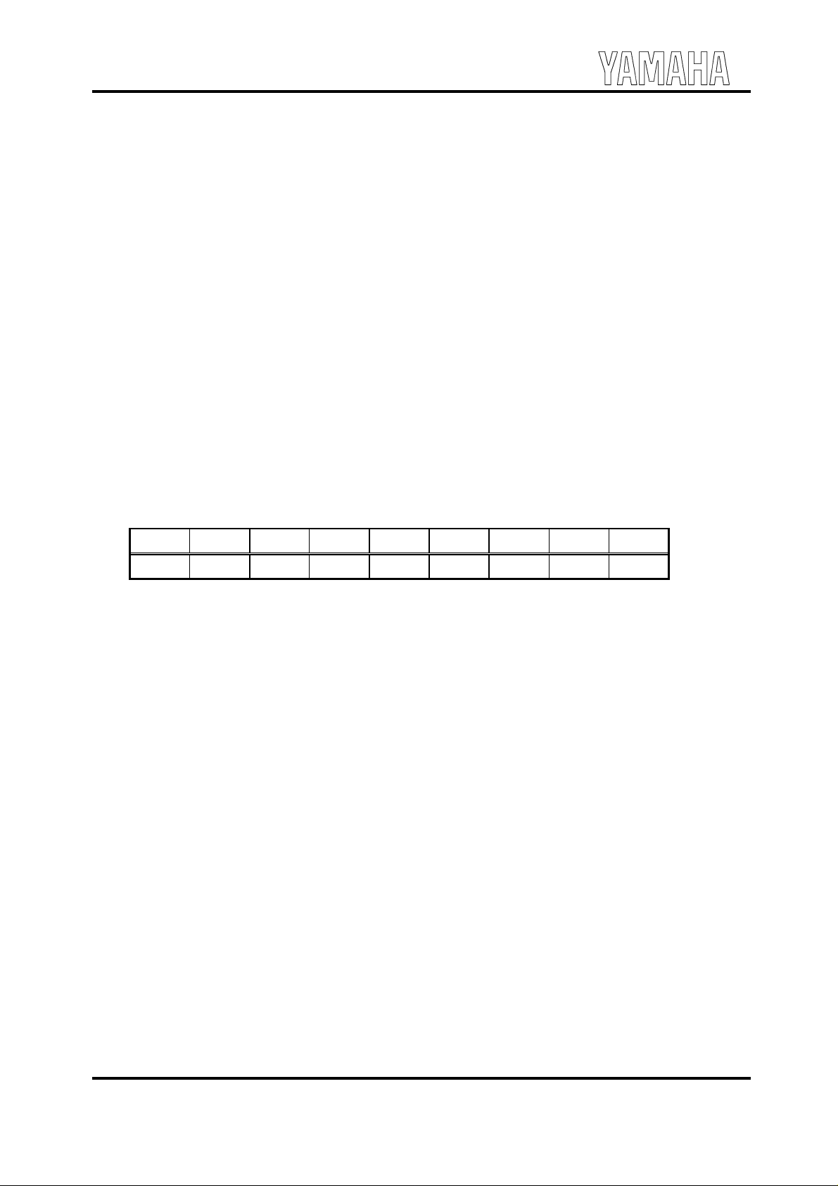
AddressD7D6D5D4D3D2D1D0
xxh IRQ FT1 FT2 - - BUSY - BUSY
-25-
January 14, 1999
Page 26
YMF740C
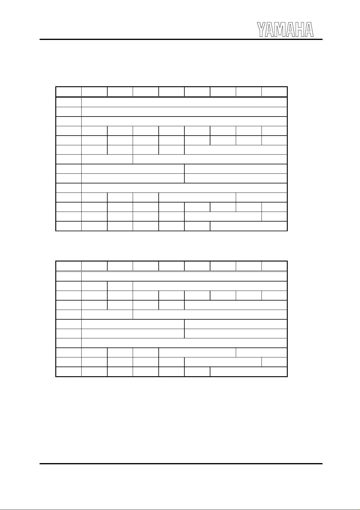
2-1-2. FM Synthesizer Data Register
FM Synthesizer Data Register Array 0 (R/W):
AddressD7D6D5D4D3D2D1D0
00-01h LSI TEST
02h TIMER 1
03h TIMER 2
04h RST MT1 MT2 - - - ST2 ST1
08h-NTS------
(*1)
20-35h
40-55h
60-75h
80-95h
A0-A8h F-NUM (L)
B0-B8h - - KON BLOCK F-NUM (H)
BDh DAM DVB RHY BD SD TOM TC HH
C0-C8h *6 *6 CHR CHL FB CNT
E0-F5h
AM VIB EGT KSR MULT
(*2)
(*3)
(*4)
(*5)
KSL TL
AR DR
SL RR
----- WS
FM Synthesizer Data Register Array 1 (R/W)
AddressD7D6D5D4D3D2D1D0
00-01h LSI TEST
04h - - CONNECTION SEL
05h - - - - - * * NEW
(*1)
20-35h
40-55h
60-75h
80-95h
A0-A8h F-NUM (L)
B0-B8h - - KON BLOCK F-NUM (H)
C0-C8h *6 *6 CHR CHL FB CNT
E0-F5h
AM VIB EGT KSR MULT
(*2)
(*3)
(*4)
(*5)
KSL TL
AR DR
SL RR
----- WS
*1 : 26h, 27h, 2Eh and 2Fh do not exist.
*2 : 46h, 47h, 4Eh and 4Fh do not exist.
*3 : 66h, 67h, 6Eh and 6Fh do not exist.
*4 : 86h, 87h, 8Eh and 8Fh do not exist.
*5 : E6h, E7h, EEh and EFh do not exist.
*6 : The bits exist, but do not function.
-26-
January 14, 1999
Page 27

YMF740C
2-2. Sound Blaster Pro Block
This block emulates the DSP commands of Sound Blaster and Sound Blaster Pro. Only playback
functions are supported (record functions are not supported). However, to maintain compatibility for
games, it is designed so that every DSP command receives a correct response.
The DMA transfer of this block uses PC/PCI protocol.
The following shows the SBBase I/O map of SB Pro.
SBBase (R) FM Synthesizer Status port
SBBase (W) FM Synthesizer Addr ess port for Register Array 0
SBBase+1h (R/W) FM Synthesizer Data register
SBBase+2h (W) FM Synthesizer Address port for Register Array 1
SBBase+3h (R/W) FM Synthesizer Data port
SBBase+4h (W) SB Mixer Address port
SBBase+5h (R/W) SB Mixer Data port
SBBase+6h (W) SB DSP Reset port
SBBase+8h (R) FM Synthesizer Status port
SBBase+8h (W) FM Synthesizer Address port for Register Array 0
SBBase+9h (R/W) FM Synthesizer Data port
SBBase+Ah (R) DSP Read Data port
SBBase+Ch (R) DSP Write-buffer status port
SBBase+Ch (W) DSP Write Command/Data port
SBBase+Eh (R) DSP Read-buffer status port
-27-
January 14, 1999
Page 28

YMF740C
2-2-1. DSP Command
The following shows the list of DSP Commands that are supported by the SB Pro engine. Both SB and
SB Pro commands are supported.
CMD Support Function
10h o 8bit direct mode single byte digitized sound output
14h o 8bit single-cycle DMA mode digitized sound output
16h 8bit to 2bit ADPCM single-cycle DMA mode digitized sound output
17h 8bit to 2bit ADPCM single-cycle DMA mode digitized sound output with ref. byte
1Ch o 8bit auto-init DMA mode digitized sound output
1Fh 8bit to 2bit ADPCM auto-init DMA mode digitized sound output with ref. byte
20h(*1) o 8bit direct mode single byte digitized sound input
24h(*1) o 8bit single-cycle DMA mode digitized sound input
2Ch(*1) o 8bit auto-init DMA mode digitized sound input
30h o Polling mode MIDI input
31h o Interrupt mode MIDI input
34h o UART polling mode MIDI I/O
35h o UART interrupt mode MIDI I/O
36h(*2) o UART polling mode MIDI I/O with time stamping
37h(*2) o UART interrupt mode MIDI I/O with time stamping
38h o MIDI output
40h o Set digitized sound transfer Time Constant
48h o Set DSP block transfer size
74h o 8bit to 4bit ADPCM single-cycle DMA mode digitized sound output
75h o 8bit to 4bit ADPCM single-cycle DMA mode digitized sound output with ref. byte
76h 8bit to 3bit ADPCM single-cycle DAM mode digitized sound output
77h 8bit to 3bit ADPCM single-cycle DMA mode digitized sound output with ref. byte
7Dh o 8bit to 4bit ADPCM auto-init DMA mode digitized sound output with ref. byte
7Fh 8bit to 3bit ADPCM auto-init DMA mode digitized sound output with ref. byte
80h o Pause DAC for a duration
90h o 8bit high-speed auto-init DMA mode digitized sound output
91h o 8bit high-speed single-cycle DMA mode digitized sound output
98h(*1) o 8bit high-speed auto-init DMA mode digitized sound input
99h(*1) o 8bit high-speed single-cycle DMA mode digitized sound input
A0h(*1) o Set input mode to mono
A8h(*1) o Set input mode to stereo
D0h o Pause 8bit DMA mode digitized sound I/O
D1h(*3) o Turn on speaker
D3h(*3) o Turn off speaker
D4h o Continue 8bit DMA mode digitized sound I/O
D8h o Get speaker status
DAh o Exit 8bit auto-init DMA mode digitized sound I/O
E1h o Get DSP version number
Note:
(*1) The SB Block responds correctly to the commands for recording and also executes the DMA transfer.
80h is always transferred.
(*2) Only output is supported for this command.
(*3) This command only changes Speaker Status (D8h).
Undocumented commands other than the ones listed above are also supported.
January 14, 1999
-28-
Page 29
YMF740C
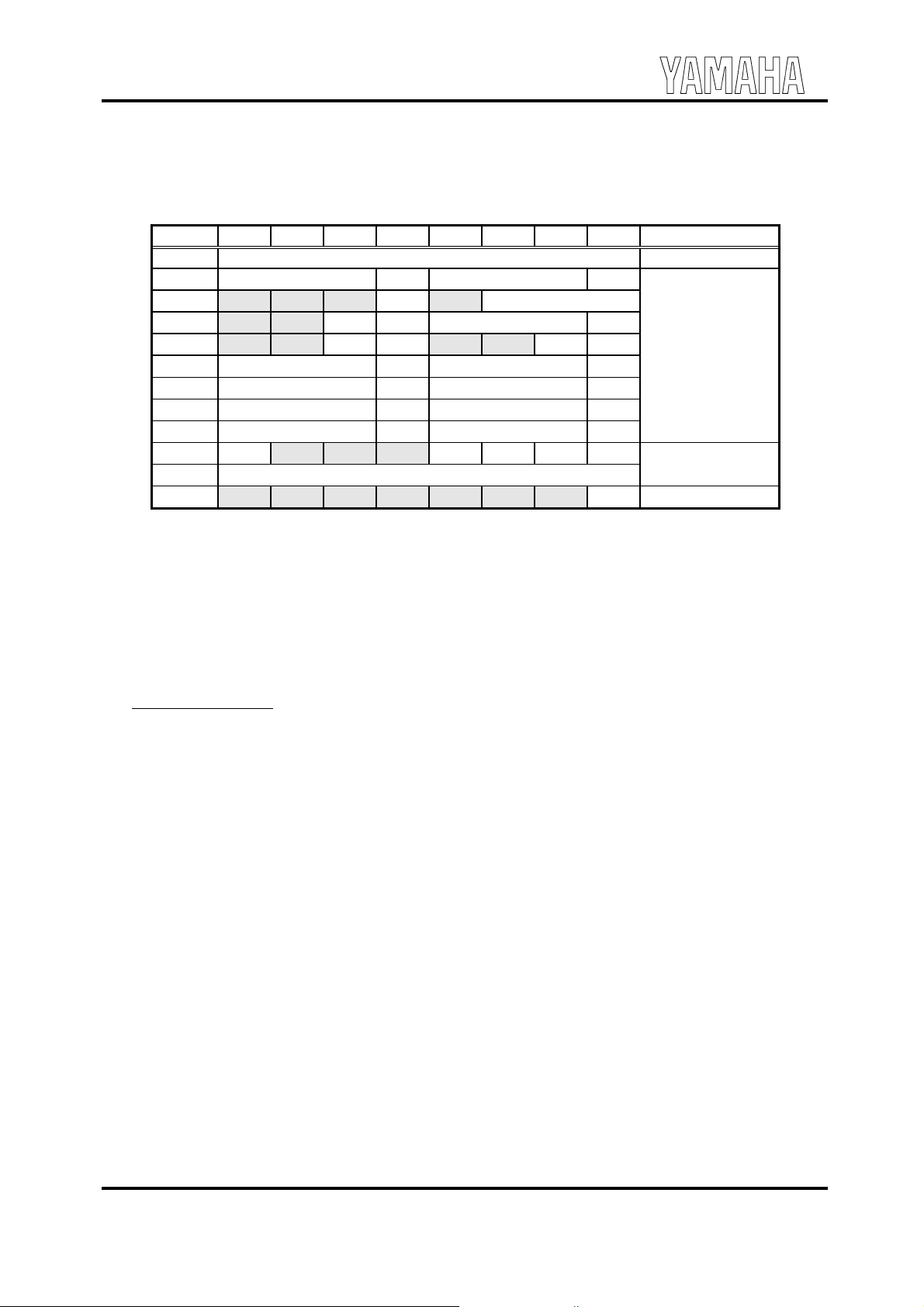
2-2-2. Sound Blaster Pro Mixer
The following shows the register map of the Mixer section of Sound Blaster Pro.
Addressb7b6b5b4b3b2b1b0 Remark
00h Reset
04h Voice Volume L "1" Voice Volume R "1"
0Ah - - - "1" - MIC Volume*
0Ch - 0Eh - - Ofilter* "1" - - St. SW "1"
22h Master V ol ume L "1" Master Volume R "1"
26h MIDI Volume L "1" MIDI Volume R "1"
28h CD Volume L* "1" CD Volume R* "1"
2Eh Line Volume L* "1" Line Volume R* "1"
F0h SBPDA - - - SS SM SE SBPDR
F1h SCAN DATA
F8h - - - - - - - SBI IRQ Status
Ifilter*
"1"
Input Source*
"1"
SB Pro Mixer
Suspend / Resume
The registers marked with * exist, but do not function.
DS-1L does not have the circuit that corresponds to the SB Mixer. T herefore, the volume settings on the
SB Mixer are converted to the DSP coefficients of DS-1L or to AC’97 register values.
The conversion for each case is described below.
(1) SB Mixer ® DSP
The volume of master, MIDI and Voice, are applied to this case.
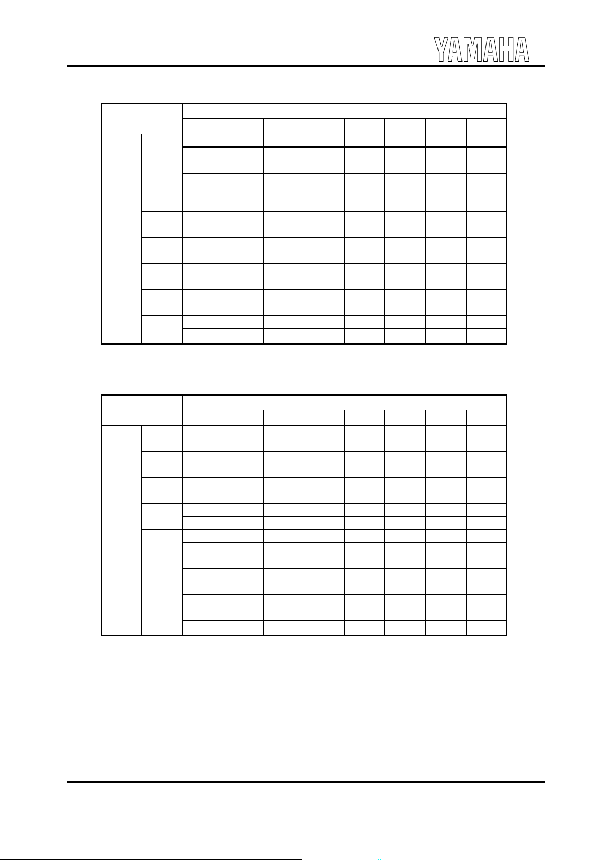
When the SB register is set, a 14-bit coefficient value is determined from the following conversion table
and used as the DSP coefficient. The attenuation value of Master Volume, MIDI, and voice are summed
together to obtain the coefficient.
These volumes cannot be controlled from PCI Audio block.
-29-
January 14, 1999
Page 30
YMF740C
(1) Volume for MIDI
0
1
2
3
4
Master Vol. (22h)
5
6
7
MIDI Vol. (26h)
01234567
mute mute mute mute mute mute mute mute
0000h 0000h 0000h 0000h 0000h 0000h 0000h 0000h
mute -52dB -42dB -36dB -32dB -30dB -28dB -26dB
0000h 0029h 0082h 0103h 019Bh 0206h 028Ch 0335h
mute -42dB -32dB -26dB -22dB -20dB -18dB -16dB
0000h 0082h 019Bh 0335h 0515h 0666h 080Eh 0A24h
mute -36dB -26dB -20dB -16dB -14dB -12dB -10dB
0000h 0103h 0335h 0666h 0A24h 0CC5h 1013h 143Dh
mute -32dB -22dB -16dB -12dB -10dB -8dB -6dB
0000h 019Bh 0515h 0A24h 1013h 143Dh 197Ah 2013h
mute -30dB -20dB -14dB -10dB -8dB -6dB -4dB
0000h 0206h 0666h 0CC5h 143Dh 197Ah 2013h 2861h
mute -28dB -18dB -12dB -8dB -6dB -4dB -2dB
0000h 028Ch 080Eh 1013h 197Ah 2013h 2861h 32D6h
mute -26dB -16dB -10dB -6dB -4dB -2dB 0dB
0000h 0335h 0A24h 143Dh 2013h 2861h 32D6h 3FFFh
The default is Master = 4, MIDI = 4 (-12dB).
(2) Volume for Voice
01234567
0
1
2
3
4
Master Vol. (22h)
5
6
7
mute mute mute mute mute mute mute mute
0000h 0000h 0000h 0000h 0000h 0000h 0000h 0000h
mute -56dB -46dB -40dB -36dB -34dB -32dB -30dB
0000h 0019h 0052h 00A3h 0103h 0146h 019Bh 0206h
mute -46dB -36dB -30dB -26dB -24dB -22dB -20dB
0000h 0052h 0103h 0206h 0335h 0409h 0515h 0666Eh
mute -40dB -30dB -24dB -20dB -18dB -16dB -14dB
0000h 00A3h 0206h 0409h 0666h 080Eh 0A24h 0CC5h
mute -36dB -26dB -20dB -16dB -14dB -12dB -10dB
0000h 0103h 0335h 0666h 0A24h 0CC5h 1013h 143Dh
mute -34dB -24dB -18dB -14dB -12dB -10dB -8dB
0000h 0146h 0409h 080Eh 0CC5h 1013h 143Dh 197Ah
mute -32dB -22dB -16dB -12dB -10dB -8dB -6dB
0000h 019Bh 0515h 0A24h 1013h 143Dh 197Ah 2013h
mute -30dB -20dB -14dB -10dB -8dB -6dB -4dB
0000h 0206h 0666h 0CC5h 143Dh 187Ah 2013h 2861h
The default is Master = 4, Voice = 4 (-16dB).
Voice Vol. (04h)
(2) SB Mixer ® AC’97
The volume of CD, Line and MIC are applied to this case. AC’97 volume are not updated automatically
when these values are changed. Thus, the SB Mixer values need to be written to the AC’97 register with
the software.
January 14, 1999
-30-
Page 31
YMF740C
2-2-3. SB Suspend / Resume
The SB block can read the internal state as to support Suspend and Resume functions. The internal state
is made up of 218 flip flops. T o read the state, these states are shifted in order and read 8 bits at a time
from the SCAN DATA register.
These registers are mapped to the SB Mixer space (see SB Mixer Register map). The registers have the
following functions.
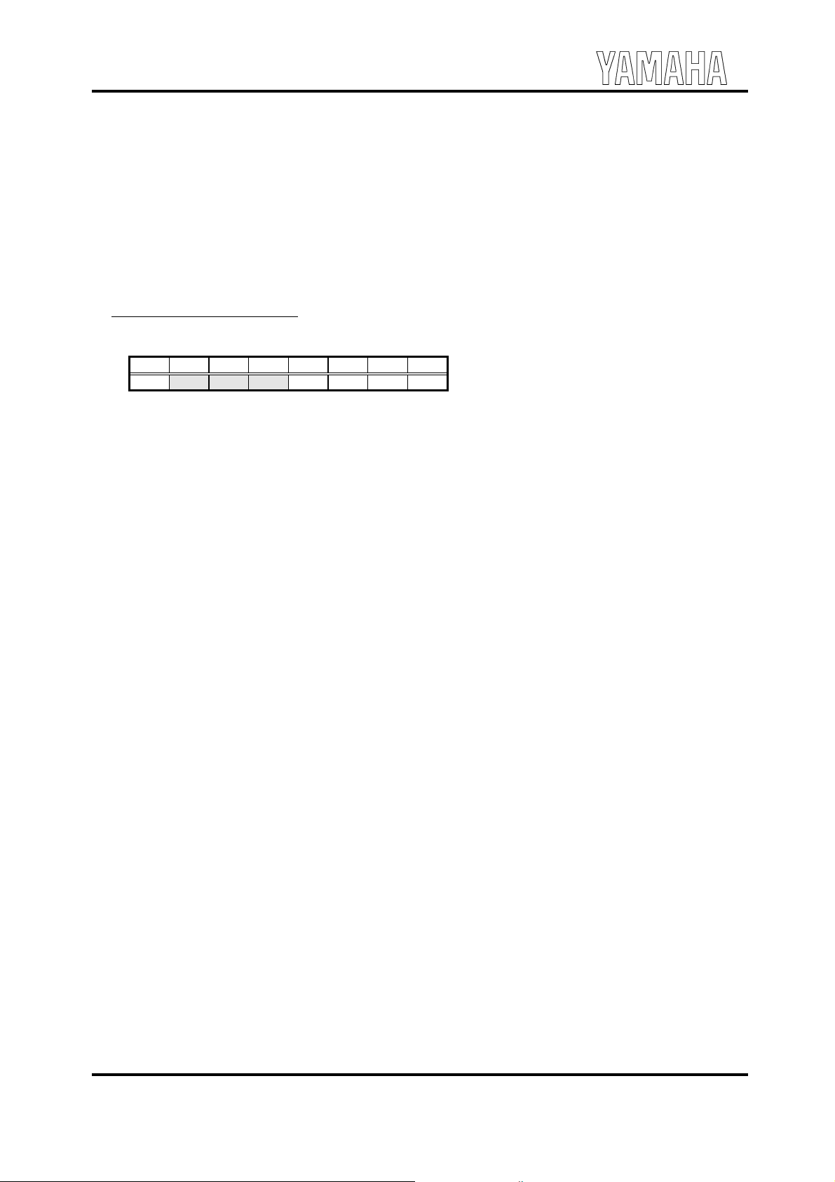
F0h: Scan In/ Out Control
Read / Write
Default: 00h
b7 b6 b5 b4 b3 b2 b1 b0
SBPDA
b0................SBPDR: Sound Blaster Power Down Request
This bit stops the internal state of the Sound Blaster blo c k.
“0”: Normal (default)
“1”: Stop
- - - SS SM SE
SBPDR
b1................SE: Scan Enable
This bit Shifts the internal state by 1 bit. Setting a “1” followed by a “0” shifts the internal state.
b2................SM: Scan Mode
This bit sets whether to read or write the state.
“0”: Write (default)
“1”: Read
b3................SS: Scan Select
This bit gives permission to read or write the internal data to the SCAN DATA register.
“0”: Normal operation (Do not allow read or write). (default)
“1”: Allow read and write.
b7................SBPDA: Sound Blaster Power Down Acknowledgement
This bit indicates that the SB Block is ready to read or write to the internal state after setting SBPDR.
This bit is read only.
“0”: Read/Write not possible
“1”: Read/ Write possible
-31-
January 14, 1999
Page 32
YMF740C
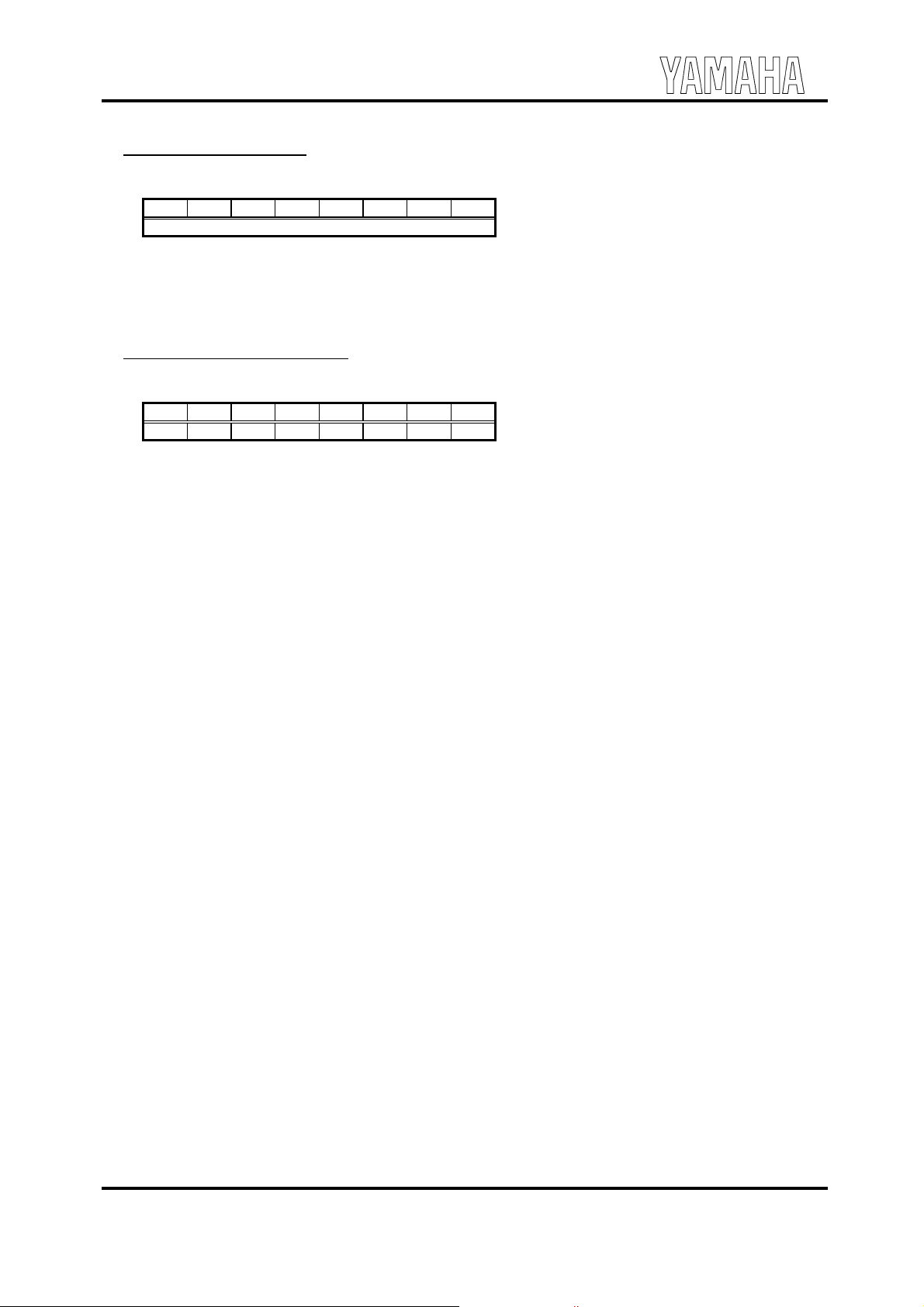
F1h: Scan In/ Out Data
Read / Write
Default: 00h
b7 b6 b5 b4 b3 b2 b1 b0
b[7:0]..........SCAN DATA
This is the data port for reading and writing the internal state.
F8h: Interrupt Flag Register
Read Only
Default: 00h
b7 b6 b5 b4 b3 b2 b1 b0
-------SBI
b0................SBI: SB Interrupt Flag
This bit indicates that the SB DSP occurs the interrupt. T his bit is read only. Thus, read the SB DSP
read port to clearing the interrupt and this bit. Then, the value of the read port is invalid.
SCAN DATA
-32-
January 14, 1999
Page 33
YMF740C
2-3. MPU401
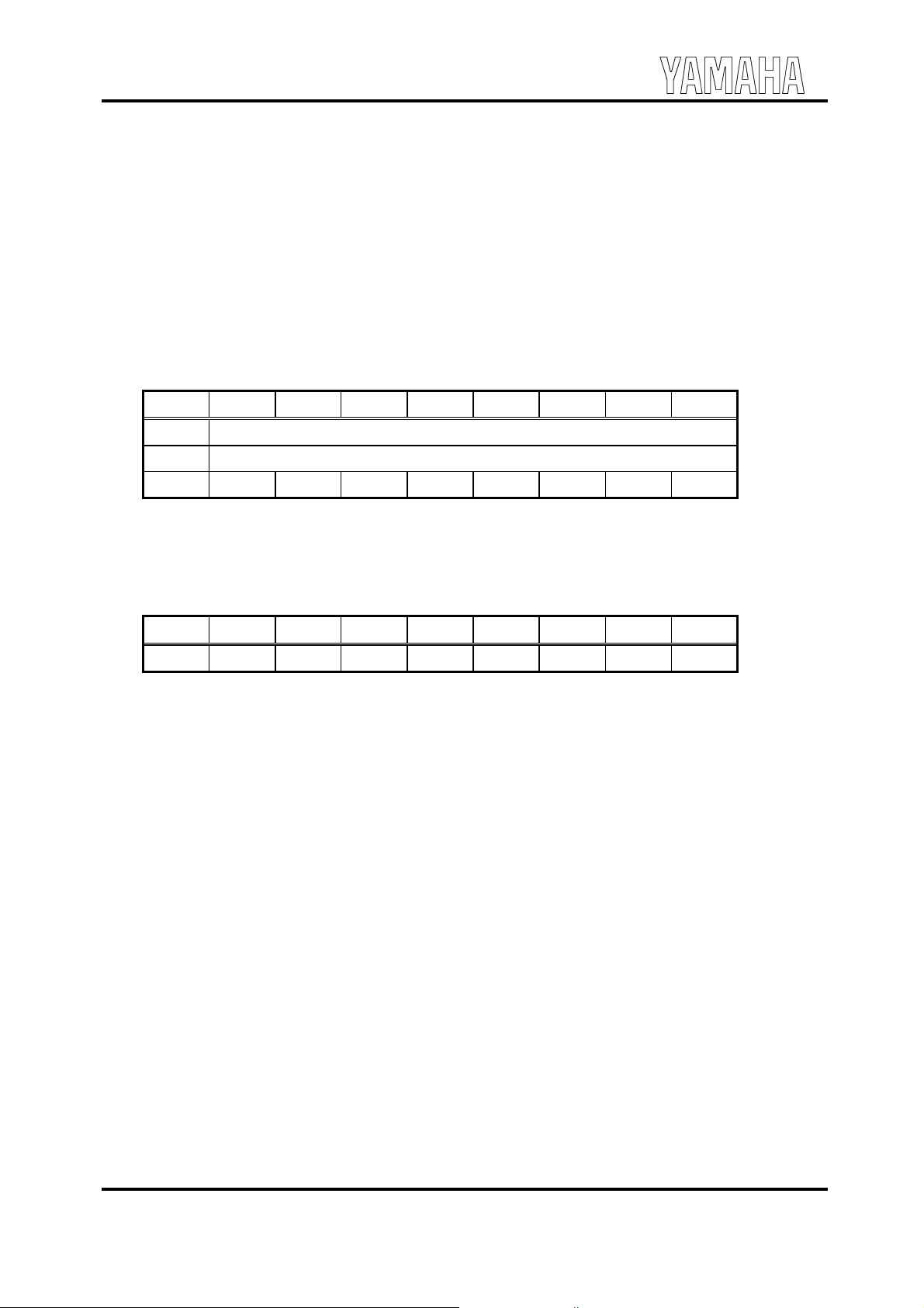
This block is for transmitting and receiving MIDI data. It is compatible with UART mode of “MPU401”.
Full duplex operation is possible using the 16-byte FIFO for each direction, transmitting and receiving.
The following shows the MPUBase I/O map for MPU401.
MPUBase (R/W) MIDI Data port
MPUBase + 1h (R) Status Register port
MPUBase + 1h (W) Command Register port
portD7D6D5D4D3D2D1D0
+0h Data
+1h (W) Command
+1h (R)/DSR/DRR------
2-4. Joystick
JSBase (R/W)
portD7D6D5D4D3D2D1D0
+0h JBB2 JBB1 JAB2 JAB1 JBCY JBCX JACY JACX
JACX... Joystick A, Coordinate X
JACY... Joystick A, Coordinate Y
JBCX... Joystick B, Coordinate X
JBCY... Joystick B, Coordinate Y
JAB1... Joystick A, Button 1
JAB2... Joystick A, Button 2
JBB1... Joystick B, Button 1
JBB2... Joystick B, Button 2
-33-
January 14, 1999
Page 34
YMF740C
g
3. DMA Emulation Protocol
The former synthesizer LSI for the ISA bus such as the Sound Blaster used the DMA controller (8237: ISA
DMAC) on the system to transfer the sound data from/to the host.
For DS-1L, however, ISA DMAC must be used to transfer the sound data to the Sound Blaster Pro Block of
the Legacy Audio Block.
Because signals to connect to the ISA DMAC are generally not available on the PCI bus, there is a way, that
is PC/PCI, proposed from the industry to emulate the ISA DMAC on the PCI bus.
DS-1L supports the protocol for transferring SB Pro sound data on the PCI bus.
3-1. PC/PCI
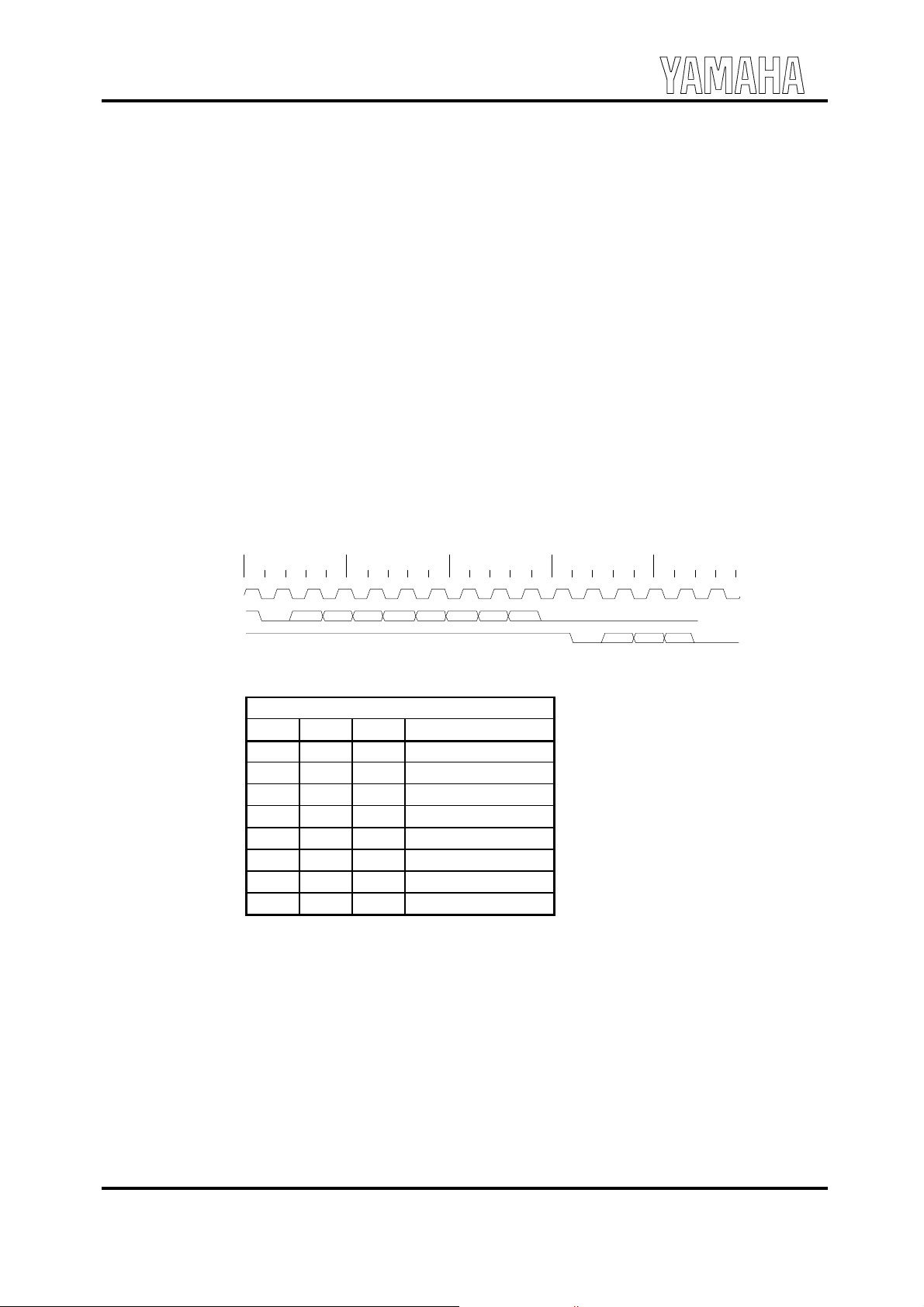
DS-1L provides two signals, PCREQ# and PCGNT# to realize the PC/PCI. The format of the signals is
shown below. DS-1L asserts PCREQ# and sets PCREQ# to “HIGH” using the PCICLK corresponding to
the DMA channel it is going to use.
In addition, DS-1L determines whether the next PCI I/O cycle is its own from the channel information that is
encoded in PCGNT#.
0ns 100ns 200ns 300ns 400ns
PCICLK
REQ#
GNT#
PCGNT# is encoded as follows.
DS-1L supports only 8-bit DMA channels (DMA Channel 0-3). It also only supports Single DMA transfer.
start CH0 CH1 CH2 CH3 CH4 CH5 CH6 CH7
GNT# Encodin
bit2 bit1 bit0
000
001
010
011
100
101
110
111
GNT# Bits
DMA Channel 0
DMA Channel 1
DMA Channel 2
DMA Channel 3
Reserved
DMA Channel 5
DMA Channel 6
DMA Channel 7
start bit0 bit1 bit2
January 14, 1999
-34-
Page 35
YMF740C
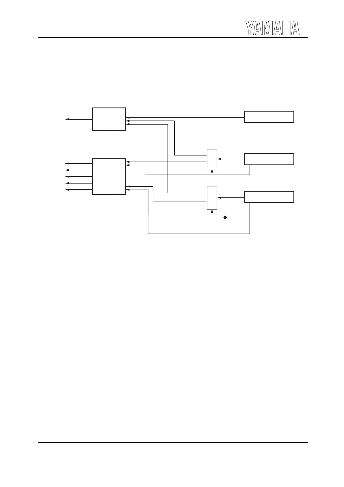
4. Interrupt Routing
DS-1L supports two types of interrupts, interrupt signal on the PCI bus (INTA#) and interrupt signal on the
ISA bus (IRQ[5,7,9,10,11]).
The IRQs on DS-1L are routed as shown below.
INTA#
IRQ5
IRQ7
IRQ9
IRQ10
IRQ11
INTA
ISA IRQ
IMOD=1
IMOD=0
IMOD=1
IMOD=0
IRQ
SelectorSelector
Select Signal
IRQ
IMOD
Select Signal
PCI Audio
Sound Blaster Pro
SBIRQ[2:0]
MPU401
MPUIRQ[2:0]
PCI Audio can only use INTA#, but the Sound Blaster Pro and MPU401 blocks of the Legacy Audio Block
can use any of the two protocols.
The protocol can be switched using 42-43h (Legacy Audio Control Register) of the PCI Configuration
Register.
-35-
January 14, 1999
Page 36
YMF740C
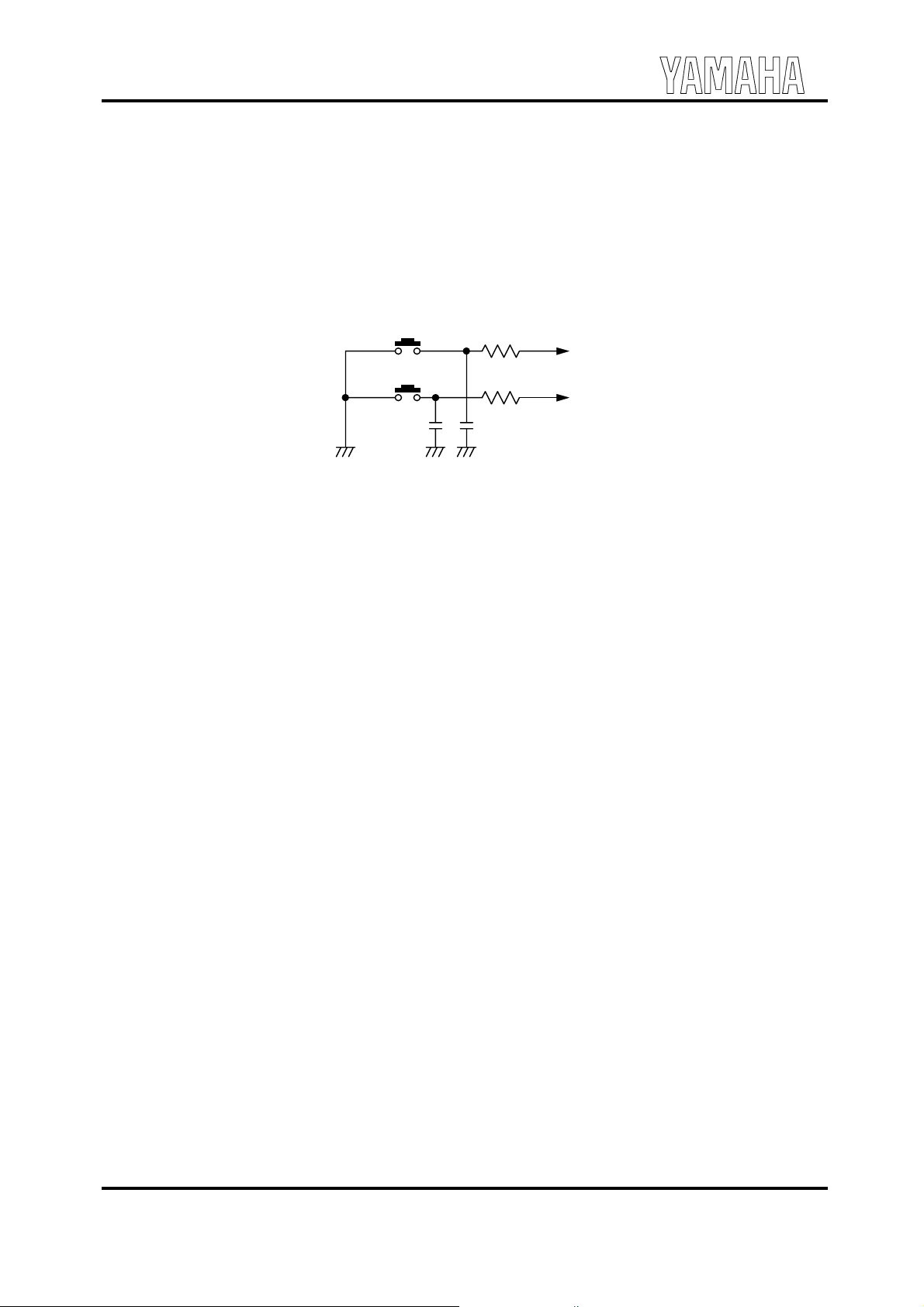
5. Hardware Volume Control
The hardware volume control determines the AC’97 master volume without using any software control using
the external circuit listed below.
Two pins, VOLUP# for increasing the volume and VOLDW# for decreasing the volume, are used.
Push SW
Push SW
1000p 1000p
DS-1L provides a shadow register for the AC’97 master volume. When the software accesses the AC’97
Master Volume, it is always reflected in the shadow register.
The value of the shadow register is incremented by 1.5dB on the rising edge of the signal input to the
VOLUP# pin. If it is already set to the maximum value, it does not change. T he value set in the shadow
register automatically updates the AC’97 master volume register through the AC-Link.
The value of the shadow register is decremented by 1.5dB on the rising edge of the signal input to the
VOLDW# pin. If it is already set to the minimum value, it does not change. The value set in the shadow
register automatically updates the AC’97 master volume register through the AC-Link.
Also, when both VOLUP#, VOLDW# pins are at LOW level, the MUTE bit of the shadow address is enabled
and the Master Volume Mute bit of the AC’97 register is automatically set through the AC-Link. When a
1k
VOLUP#
1k
VOLDW#
rising edge is dete cted on either VOLUP# or VOLDW#, the MUTE bit is reset through the AC-Link. The
Master Volume is set to the value before the Mute.
If the AC-Link is BUSY (when controlling the register from the AC’97 Control Register), the value in the
shadow register is set to AC’97 on the next frame. The AC’97 Control Register is set to BUSY in this case.
When the master volume changes or is muted due to VOLUP#, VOLDW#, an interrup t is generated at the
host.
The interrupt is used to notify the driver that the Master Volume has been changed from the outside.
January 14, 1999
-36-
Page 37
YMF740C
ELECTRICAL CHARACTERISTICS
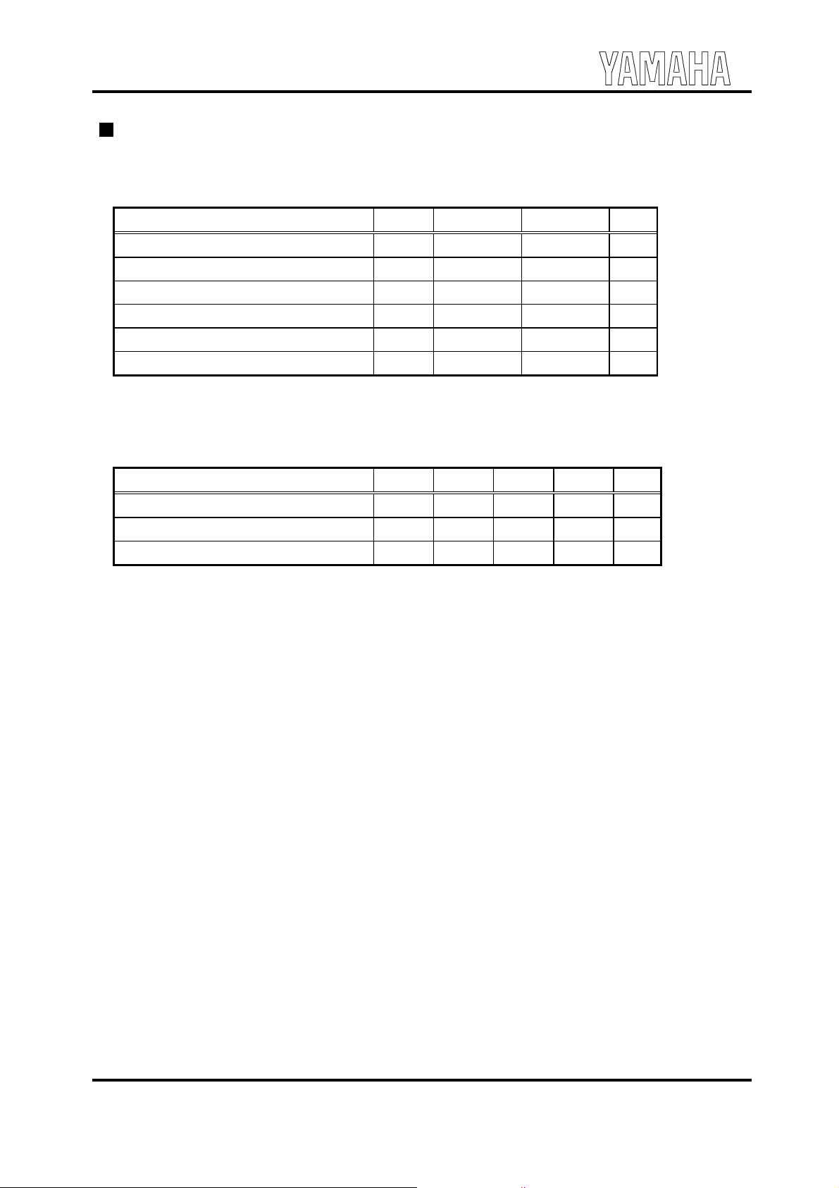
1. Absolute Maximum Ratings
Item Symbol Min. Max. Unit
Power Supply Voltage 1 (PVDD, VDD5) V
Power Supply Voltage 2 (VDD3, LVDD) V
Input Voltage 1 (PVDD, VDD5) V
Input Voltage 2 (VDD3, LVDD) V
Operating Ambient Temperature T
Storage Temperature T
DD5
DD3
IN5
IN3
OP
STG
Note : PVSS=LVSS=VSS=0[V]
2. Recommended Operating Conditions
Item Symbol Min. Typ. Max. Unit
Power Supply Voltage 1 (PVDD, VDD5) V
Power Supply Voltage 2 (VDD3, LVDD) V
Operating Ambient Temperature T
Note : PVSS=LVSS=VSS=0[V]
DD5
DD3
OP
-0.5 7.0 V
-0.3 4.6 V
-0.5 V
-0.3 V
+0.5 V
DD5
+0.3 V
DD3
070°C
-50 125 °C
4.75 5.00 5.25 V
3.00 3.30 3.60 V
02570°C
-37-
January 14, 1999
Page 38
YMF740C
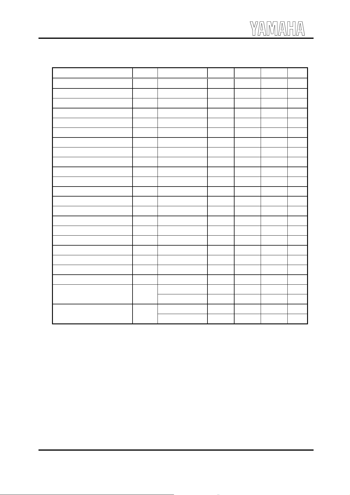
3. DC Characteristics
Item Symbol Condition Min. Typ. Max. Unit
High Level Input Voltage 1 V
Low Level Input Voltage 1 V
High Level Input Voltage 2 V
Low Level Input Voltage 2 V
High Level Input Voltage 3 V
Low Level Input Voltage 3 V
High Level Input Voltage 4 V
Low Level Input Voltage 4 V
Input Leakage Current I
High Level Output Voltage 1 V
Low Level Output Voltage 1 V
High Level Output Voltage 2 V
Low Level Output Voltage 2 V
High Level Output Voltage 3 V
Low Level Output Voltage 3 V
High Level Output Voltage 4 V
Low Level Output Voltage 4 V
Input Pin Capacitance C
Clock Pin Capacitance C
IDSEL Pin Capacitance C
Output Leakage Current I
*1 2.2 V
IH1
*1 -0.5 0.8 V
IL1
*2 2.2 V
IH2
*2 -0.5 0.6 V
IL2
*3 2.2 V
IH3
*3 0.8 V
IL3
*4 0.7V
IH4
*4 0.2V
IL4
0< VIN < V
IL
*5, I
OH1
*5, I
OL1
*6, I
OH2
*6, I
OL2
*7, I
OH3
*7, I
OL3
*8, I
OH4
*8, I
OL4
515pF
IN
515pF
CLK
515pF
IDSEL
OL
DD5
= -1mA 2.4 V
OH1
= 3mA 0.55 V
OL1
= -2mA 2.4 V
OH2
= 6mA 0.55 V
OL2
= -4mA 2.4 V
OH3
= 12mA 0.55 V
OL3
= -80µA V
OH4
= 2mA 0.4 V
OL4
DD5
-10 10 µA
-1.0 V
DD5
-10 10 µA
+0.5 V
DD5
+0.5 V
DD5
DD5
V
V
Power Supply Current 1 PVDD+VDD5 60 mA
(Normal Operation) VDD3 145 mA
Power Supply Current 2 *9, PVDD+VDD5 0.5 2 mA
(Power Save) *9, VDD3 6 10 mA
Note : Top = 0~70°C, PVDD=5.0±0.25[V], VDD5=5.0±0.25[V], VDD3=3.3±0.3[V], LVDD=3.3±0.3[V], CL=50 pF
*1: Applicable to all PCI Iuput/Output pins and Iunput pins except PCICLK and RST# pin.
*2: Applicable to RST# pin.
*3: Applicable to CBCLK, CSDI, GP[7:4], RXD and TEST[7:0]# pins.
*4: Applicable to XI24 pin.
*5: Applicable to AD[31:0], C/BE[3:0]#, PAR, REQ#, PCREQ#, SERIRQ# and TXD pins.
*6: Applicable to FRAME#, IRDY#, TRDY#, STOP#, DEVSEL#, PERR#, SERR#, CRST#, CSYNC and CSDO
pins.
*7: Applicable to IRQ5, IRQ7, IRQ9, IRQ10, IRQ11 and INTA# pins.
*8: Applicable to CMCLK and XO24 pins.
*9: DS-1L Power Control Register, DMC=DPLL0=DPLL1=PSN=PSL0=PSL1=“1”, PCICLK (33MHz) is stopped.
-38-
January 14, 1999
Page 39
YMF740C
4. AC Characteristics
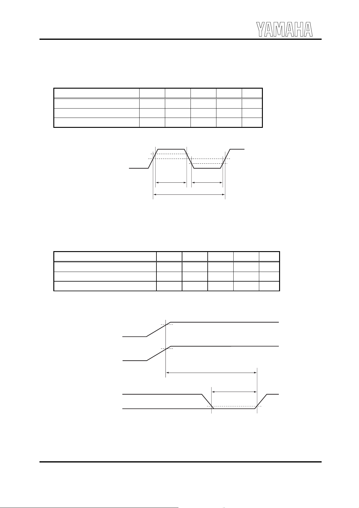
4-1. Master Clock (Fig.1)
Item Symbol Min. Typ. Max. Unit
XI24 Cycle Time t
XI24 High Time t
XI24 Low Time t
Note : Top = 0-70°C, PVDD=5.0±0.25 V, VDD5=5.0±0.25 V, VDD3=3.3±0.3 V, LVDD=3.3±0.3 V
XICYC
XIHIGH
XILOW
XI24
- 40.69 - ns
16 - 24 ns
16 - 24 ns
3.5 V
t
XIHIGH
t
XICYC
t
XILOW
2.5 V
1.0 V
Fig.1: XI24 Master Clock timing
4-2. Reset (Fig.2)
Item Symbol Min. Typ. Max. Unit
Reset Active Time after Power Stable t
Power Stable to Reset Rising Edge t
RST
RSTOFF
1--ms
10 - - ms
Reset Slew Rate - 50 - - mV/ns
Note : Top = 0-70°C, PVDD=5.0±0.25 V, VDD5=5.0±0.25 V, VDD3=3.3±0.3 V, LVDD=3.3±0.3 V, CL=50 pF
PVDD, VDD5
L VDD, VDD3
RST#
4.75 V
3.0 V
Fig.2: PCI Reset timing
-39-
t
RSTOFF
t
RST
0.6 V
January 14, 1999
Page 40
YMF740C
)
)
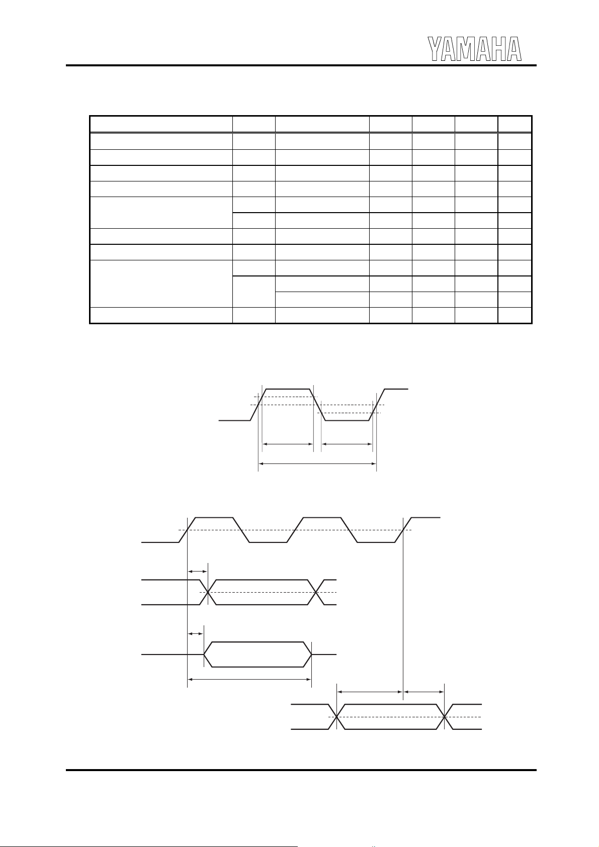
4-3. PCI Interface (Fig.3, 4)
Item Symbol Condition Min. Typ. Max. Unit
PCICLK Cycle Time t
PCICLK High Time t
PCICLK Lo w Time t
PCYC
PHIGH
PLOW
30 - - ns
11 - - ns
11 - - ns
PCICLK Slew Rate - 1 - 4 V/ns
t
PCICLK to Signal Valid Delay
Float to Active Delay t
Active to Float Delay t
PVAL
t
PVAL(PTP
PON
POFF
t
PSU
t
PSU(PTP
Input Hold Time for PCICLK t
Note : Top = 0-70°C, PVDD=5.0±0.25 V, VDD5=5.0±0.25 V, VDD3=3.3±0.3 V, LVDD=3.3±0.3 V, CL=50 pF
*10: This characteristic is applicable to REQ# and PCREQ# signal.
*11: This characteristic is applicable to GNT# and PCGNT# signal.
PCICLK
(Bused signal) 2 - 11 ns
(Point to Point) 2 - 12 ns
2--ns
--28ns
(Bused signal) 7 - - ns
*10 (Point to Point) 10 - - nsInput Setup Time to PCICLK
*11 (Point to Point) 12 - - ns
PH
2.2 V
0--ns
1.5 V
0.8 V
PCICLK
OUTPUT
Tri-State
OUTPUT
t
t
PVAL
PON
t
PHIGH
t
PCYC
Fig.3: PCI Clock timing
t
POFF
INPUT
t
PLOW
1.5 V
t
PSU
1.5 V
t
PH
1.5 V
Fig.4: PCI Bus Signals timing
January 14, 1999
-40-
Page 41
YMF740C
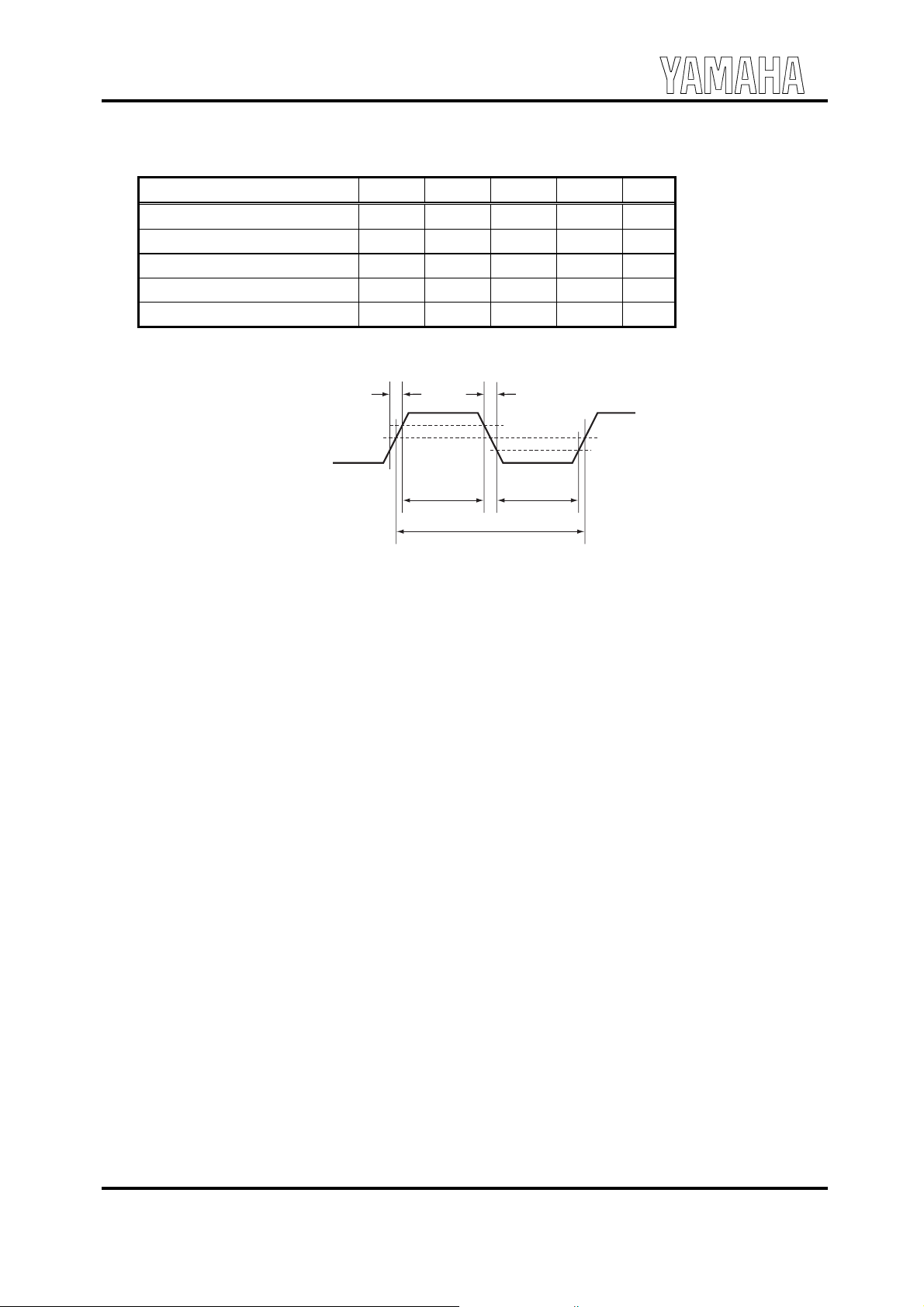
4-4. AC’97 Master Clock (Fig.5)
Item Symbol Min. Typ. Max. Unit
CMCLK Cycle Time t
CMCLK High Time t
CMCLK Low Time t
CMCLK Rising Time t
CMCLK Falling Time t
Note : Top = 0-70°C, PVDD=5.0±0.25 V, VDD5=5.0±0.25 V, VDD3=3.3±0.3 V, LVDD=3.3±0.3 V, CL=50 pF
t
CMR
CMCYC
CMHIGH
CMLOW
CMR
CMF
CMCLK
- 40.69 - ns
8--ns
8--ns
-4.6-ns
-2.1-ns
t
CMF
t
CMHIGH
t
CMCYC
3.5 V
t
CMLOW
2.5 V
0.4 V
Fig.5: Master Clock timing for AC’97
-41-
January 14, 1999
Page 42
YMF740C
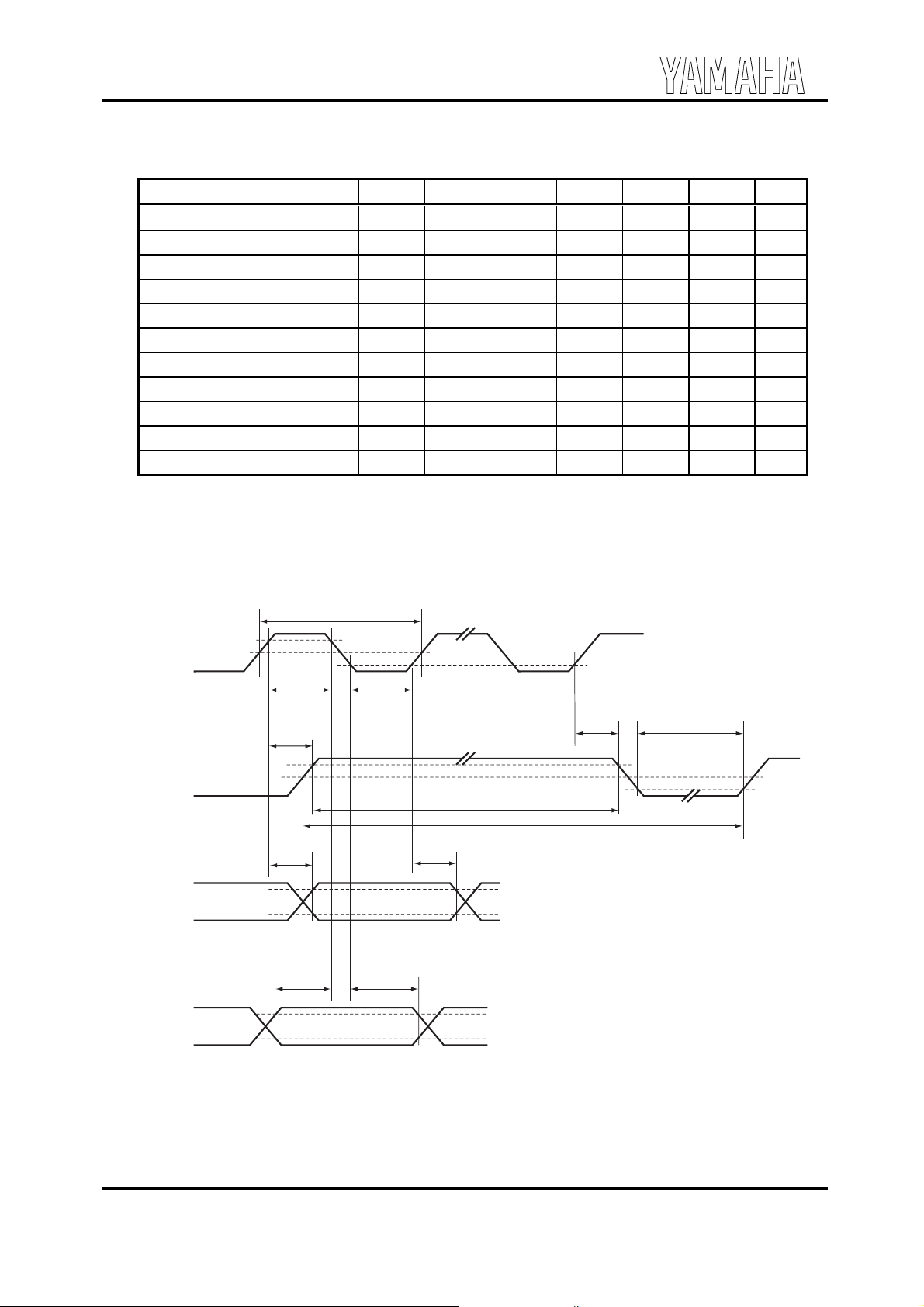
4-5. AC-link (Fig.6)
Item Symbol Condition Min. Typ. Max. Unit
CBCLK Cycle Time t
CBCLK High Time t
CBCLK Low Time t
CSYNC Cycle Time t
CSYNC High Time t
CSYNC Low Time t
CBCLK to Signal Valid Delay t
Output Hold Time for CBCLK t
Input Setup Time to CBCLK t
Input Hold Time for CBCLK t
CBICYC
CBIHIGH
CBILOW
CSYCYC
CSYHIGH
CSYLOW
CVAL
COH
CISU
CIH
*11 - - 20 ns
*11 0 - - ns
*12 15 - - ns
*12 5 - - ns
- 81.4 - ns
35 40.7 45 ns
35 40.7 45 ns
- 20.8 - ns
-1.3-ns
- 19.5 - ns
Warm Reset Width - 1.3 - µs
Note) Top = 0-70°C, PVDD=5.0±0.25 V, VDD5=5.0±0.25 V, VDD3=3.3±0.3 V, LVDD=3.3±0.3 V, CL=50 pF
*11: This characteristic is applicable to CSYNC and CSDO signal.
*12: This characteristic is applicable to CSDI signal.
t
CBICYC
2.2 V
CBCLK
t
CVAL
t
CBIHIGH
t
CBILOW
1.5 V
t
0.8 V
COH
2.2 V
t
CSYLOW
SYNC
t
CSYHIGH
1.5 V
0.8 V
CSDO
CSDI
t
CVAL
t
CISU
t
t
CIH
Fig.6: AC-link timing
-42-
COH
2.2 V
0.8 V
2.2 V
0.8 V
t
CSYCYC
January 14, 1999
Page 43
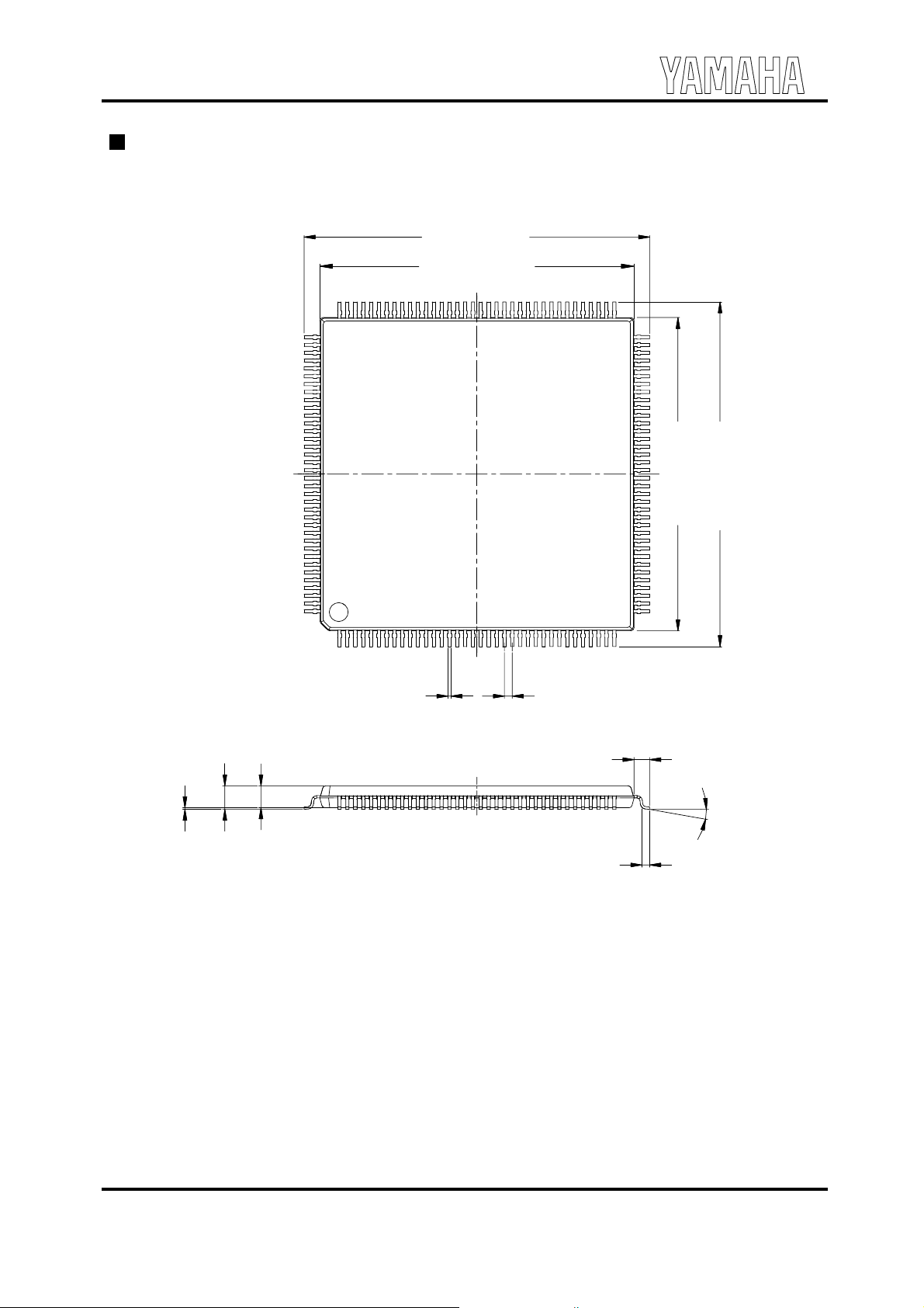
YMF740C
EXTERNAL DIMENSIONS
YMF740C-V
22.00±0.40
20.00±0.30
73108
109
144
1.70MAX.
1.40±0.20
0 MIN. (STAND OFF)
0.20±0.10 P-0.50TYP
72
20.00±0.30
22.00±0.40
37
361
(1.00)
0-10˚
LEAD THICKNESS : 0.15+0.10
-0.06
0.50±0.20
The shape of the molded corner may slightly different from the shape in this diagram.
The figure in the parenthesis ( ) should be used as a reference.
Plastic body dimensions do not include burr of resin.
UNIT : mm
Note : The LSIs for surface mount need especial consideration on storage and soldering conditions.
For detailed information, please contact your nearest agent of Yamaha.
January 14, 1999
-43-
Page 44
YMF740C
y
g
q
q
jury
IMPORTANT NOTICE
1. Yamaha reserves the right to make changes to its Products and to this document
without notice. The information contained in this document has been carefull
and is believed to be reliable. However, Yamaha assumes no responsibilities for
inaccuracies and makes no commitment to update or to keep current the information
contained in this document.
checked
2. These Yamaha Products are desi
applications, and are not suitable for other uses, such as medical life support e
nuclear facilities, critical care e
lead to death, personal in
uipment or any other application the failure of which could
or environmental or property damage. Use of the Products
ned only for commercial and normal industrial
uipment,
in any such application is at the customer's sole risk and expense.
3. YAMAHA ASSUMES NO LIABILITY FOR INCIDENTAL, CONSEQUENTIAL OR
SPECIAL DAMAGES OR INJURY THAT MAY RESULT FROM MISAPPLICATION OR
IMPROPER USE OR OPERATION O F THE PRO DUCTS.
4. YAMAHA MAKES NO WARRANTY OR REPRESENTATION THAT THE PRODUCTS
ARE SUBJECT TO INTELLECTUAL PROPERTY LICENSE FROM YAMAHA OR
ANYTHIRD PARTY, AND YAMAHA MAKES NO WARRANTY OR REPRESENTATION
OF NON-INFRINGEMENT WITH RESPECT TO THE PRODUCTS. YAMAHA
SPECIFICALLY EXCLUDES ANY LIABILITY TO THE CUSTOMER OR ANY THIRD
PARTY ARISING FROM OR RELATED TO THE PRODUCTS' I NFRING EMENT O F ANY
THIRD PARTY'S INTELLECTUAL PROPERTY RIGHTS, INCLUDING THE PATENT,
COPYRIGHT, TRADEMARK OR TRADE SECRET RIGHTS OF ANY THIRD PARTY.
5. EXAMPLES OF USE DESCRIBED HEREIN ARE MERELY TO INDICATE THE
CHARACTERISTICS AND PERFORMANCE OF YAMAHA PRODUCTS. YAMAHA
ASSUMES NO RESPONSIBILITY FOR ANY INTELLECTUAL PROPERTY CLAIMS OR
OTHER PROBLEMS THAT MAY RESULT FROM APPLICATIONS BASED ON THE
EXAMPLES DESCRIBED HEREIN. YAMAHA MAKES NO WARRANTY WITH
RESPECT TO THE PRODUCTS, EXPRESS OR IMPLIED, INCLUDING, BUT NOT
LIMITED TO THE WARRANTIES OF MERCHANTABILITY, FITNESS FOR A
PARTICULAR USE AND TITLE.
Note) The specifications of this product are subject to improvement change without prior notice.
AGENCY
Address inquires to :
Semi-conductor Sales Department
- Head Office
- Tokyo Office
- Osaka Office
- U.S.A. Office
-44-
YAMAHA CORPORATION
Iwata-gun, Shizuok a-ken, 438-0192
Tel. +81-539-62-4918 Fax. +81-539-62-5054
2-17-11, Takanawa, Minato-ku, Tokyo, 108-8568
Tel. +81-3-5488-5431 Fax. +81-3-5488-5088
1-13-17, Namba Naka, Naniwa-ku,
Osaka City, Osaka, 556-0011
Tel. +81-6-6633-3690 Fax. +81-6-6633-3691
YAMAHA Syst em Technology.
100 Century Center Court, San Jose, CA 95112
Tel. +1-408-467-2300 Fax. +1-408-437-8791
203, MatsunokiJima, Toyooka-mura.
January 14, 1999
 Loading...