


V9938
MSX-VIDEO
Technical Data Book
Programmer’s Guide
ASCII CORPORATION / NIPPON GAKKI CO., LTD.
© 2010-2015 Eugeny Brychkov
NIPPON GAKKI CO., LTD.
© 1985 ASCII CORP. / NIPPON GAKKI CO.
Page 1 of 108

This page is intentionally left blank
© 1985 ASCII CORP. / NIPPON GAKKI CO.
Page 2 of 108
© 2010-2015 Eugeny Brychkov

NOTE FROM THE EDITOR
This important technical book – including preface, dated back to 1985, had been
reworked and modified appropriately in order to give more detailed explanation of how
V9938 chip works and how to effectively program the system based on it.
While MSX gave up to the IBM PC standard as a computing platform in early 1990s, it
is still one of the powerful specimens in the field of 8-bit home entertainment and hobbyist
platforms. It is argued that modern PC architecture origins at the MSX standard; and it is
clear that initiative, taken by Microsoft and ASCII by institutionalizing software and
hardware compatibility was taken in further developments on the IT market.
V9938 is one of the most popular video-processors in the family of Texas Instruments
original chips, improved by a group of companies from Japan and US. Its follower, V9958,
was a VDP chip for limited release of MSX2+ and MSX Turbo-R machines, and the last VDP
in the family, V9990, can only be found in add-on cartridges.
The book is provided in PDF format and is searchable to allow internet search engines
indexing it so that potential readers would easily find it.
December, 2010
Eugeny Brychkov
Rev. 1.00 (Jan 06, 2011): Initial release
Rev. 1.01 (Jan 27, 2011): corrections per Daemos et al.
Rev. 1.01a (Mar 06, 2011): corrections per ARTRAG et al.
Rev. 1.01b (June 02, 2015): corrections per yzi and ARTRAG
Please log issues with this document to the following MSX Resource Center thread:
http://www.msx.org/forumtopic12176.html
© 1985 ASCII CORP. / NIPPON GAKKI CO.
Page 3 of 108
© 2010-2015 Eugeny Brychkov

This page is intentionally left blank
© 1985 ASCII CORP. / NIPPON GAKKI CO.
Page 4 of 108
© 2010-2015 Eugeny Brychkov

PREFACE
The V9938 introduced in this manual is a Very Large-Scale Integrated Circuit (VLSI)
that was developed as a video Display Processor (VDP) for the MSX2. The MSX personal
computer standard was introduced in 1983 by ASCII Corporation and Microsoft
Incorporated. At present, the MSX is manufactured and marketed worldwide. In order to
strengthen some of the functions of the original MSX, the MSX2 standard was developed in
1985. In addition to being software-compatible with the MSX, the MSX2 supports new
media and has video processing capabilities that are not available on conventional 8-bit
personal computers.
To make the MSX2 a reality, two requirements for the Video Processor were: upward
compatibility with the existing TMS9918A (the VDP for the MSX) software and increased
number of functions. The V9938 was developed through the joint efforts of ASCII
Corporation, Microsoft Incorporated, and YAMAHA.
The following functions are supported on the V9938:
Full bit-mapped mode
80-column text display
Access using X- and Y-coordinates for easier programming; the X-Y coordinates
are independent of the screen mode
Fundamental hardware commands to decrease the processing time and reduce
programming complexity
Digitize and external synchronization
Color palette (9 bits x 16 patterns)
Linear RGB video output
More sprites per horizontal line
Because the V9938 has the above functions, it provides superior video capabilities
that make it possible for its use in a variety of applications, including the MSX2. CAPTAIN
terminals and NAPLPS terminals using the V9938 have already been developed. We hope
that the V9938 will be a standard video processing device on a worldwide basis.
This manual was written to explain how to set parameters of the v9938 and is a
reference for developing applications and system software for it.
We are pleased that you have chosen to develop software for the V9938 and that you
have referred to this manual for assistance.
Finally, we would like to express our deep gratitude to the people at NTT as well as
other related manufacturers for their valuable opinions which contributed to the
development of the V9938.
August, 1985
ASCII Corporation
© 1985 ASCII CORP. / NIPPON GAKKI CO.
Page 5 of 108
© 2010-2015 Eugeny Brychkov

This page is intentionally left blank
© 1985 ASCII CORP. / NIPPON GAKKI CO.
Page 6 of 108
© 2010-2015 Eugeny Brychkov

CONTENTS
DEFINITIONS..............................................................................................9
1. BASIC INPUT AND OUTPUT.....................................................................13
1.1. Accessing the Control Registers ..............................................................13
1.1.1. Direct access to VDP registers.........................................................13
1.1.2. Indirect access to registers through R#17 (Control Register Pointer)..13
1.2. Accessing the Palette Registers...............................................................14
1.3. Accessing the Status Registers................................................................14
1.4. Accessing the Video RAM .......................................................................14
2. REGISTER FUNCTIONS............................................................................17
2.1. Control registers....................................................................................17
2.1.1. Mode registers...............................................................................17
2.1.2. Table Base address registers...........................................................18
2.1.3. Color registers ...............................................................................19
2.1.4. Display registers ............................................................................20
2.1.5. Access registers .............................................................................21
2.1.6. Command registers ........................................................................22
2.2. Status registers #0 to #9 .......................................................................23
3. SCREEN MODES.......................................................................................25
3.1. TEXT1 mode .........................................................................................25
3.2. TEXT2 mode .........................................................................................29
3.3. MULTICOLOR (MC) mode.......................................................................34
3.4. GRAPHIC1 (G1) mode ............................................................................38
3.5. GRAPHIC2 (G2) and GRAPHIC3 (G3) modes ............................................42
3.6. GRAPHIC4 (G4) mode ............................................................................47
3.7. GRAPHIC5 (G5) mode ............................................................................50
3.8. GRAPHIC6 (G6) mode ............................................................................55
3.9. GRAPHIC7 (G7) mode ............................................................................59
4. COMMANDS.............................................................................................63
4.1. Types of Commands ..............................................................................63
4.2. Page concept ........................................................................................64
4.3. Logical Operations .................................................................................65
4.4. Explanations of Commands.....................................................................66
4.4.1. HMMC (High-speed move CPU to VRAM)..........................................66
4.4.2. YMMM (High speed move VRAM to VRAM, y only) ............................69
4.4.3. HMMM (High speed move VRAM to VRAM).......................................71
4.4.4. HMMV (High-speed move VDP to VRAM)..........................................73
4.4.5. LMMC (Logical move CPU to VRAM).................................................75
4.4.6. LMCM (Logical move VRAM to CPU).................................................78
© 1985 ASCII CORP. / NIPPON GAKKI CO.
Page 7 of 108
© 2010-2015 Eugeny Brychkov

4.4.7. LMMM (Logical move VRAM to VRAM)..............................................81
4.4.8. LMMV (logical move VDP to VRAM) .................................................83
4.4.9. LINE .............................................................................................85
4.4.10. SRCH ..........................................................................................87
4.4.11. PSET...........................................................................................90
4.4.12. POINT.........................................................................................92
4.5. Speeding up the processing of commands ...............................................93
4.6. States of the registers after command execution ......................................94
5. SPRITES ..................................................................................................95
5.1. Sprite mode 1 (G1, G2, MC) ...................................................................96
5.2. Sprite mode 2 (G3, G4, G5, G6, G7)........................................................100
5.3. Special rules for sprite color settings .......................................................107
6. SPECIAL FUNCTIONS ..............................................................................108
6.1. Alternate display of two graphics screen pages ........................................108
6.2. Displaying two graphics screens at 60Hz..................................................108
6.3. Interlace display ....................................................................................108
© 1985 ASCII CORP. / NIPPON GAKKI CO.
Page 8 of 108
© 2010-2015 Eugeny Brychkov

DEFINITIONS
A
Attribute
The property of an object, which controls how object looks like on the screen. Attribute
can be a color, position of an object, or control which pixel should have specific color
B
Background
Is an
object. For example, for a character displayed on the screen the pixels of its image is said
to have foreground color, while other pixels to have background color. In case of sprites,
they may be said to appear in the foreground to the font patterns, as sprites overlap
images of the font. See also
C
Collision
Sprites are said to collide when their dots having color code 1 (simply saying – dots
identified with binary 1s in their sprite pattern generator table) overlap. In some
circumstances such behavior may be changed in favor or mixing sprite colors to have
pseudo-multi-colored sprites
Color
A property of the pixel on the screen. Color of the pixel may come from various sources:
from global color register, from pattern color table or from sprite color table. Colors can
also be coded in the palette registers through setup of red, green and blue components –
in this case, if color table of the patterns and sprites remain unchanged, actual colors,
associated with them, may be different
Command
A special sequence of VDP operations, a kind of hardware acceleration. Command is
expected to streamline CPU-VDP-VRAM operations, unload CPU and increase data transfer
speed.
E
Expansion RAM
This random access memory is used to store non-displayed data or register information,
and is not necessary for proper operation of the VDP. Maximal size or expansion RAM is
64K bytes. Due to specific purposes of this RAM, it is rarely used in applications.
object
or
property
which is perceived to be in the background to another property or
Foreground
© 1985 ASCII CORP. / NIPPON GAKKI CO.
Page 9 of 108
© 2010-2015 Eugeny Brychkov

L
Layout
A map of patterns or sprites which identify where to display specific object or which object
should be displayed in specific position. In case of patterns (font), Pattern generator Table
identifies the appearance of font, but in order to display these patterns in specific position,
programmer should put its number into Pattern Layout Table in respective location
O
Object
Font patterns or a sprite.
P
Pattern
A property of an object identifying how object looks like. Object can be a font pattern or a
sprite pattern. Pattern may be represented by one byte or 8 bytes in different modes; its
contents codes colors of the pixels displayed. For some modes, 8 bits (one byte) can code
8 pixels – 0 for background color and 1 for foreground color, in other modes 8 bits can
code 4 pixels – with colors 0, 1, 2, and 3. To display font patterns on the screen it may not
be enough to set its
pattern
, but also put its pattern number into the
layout
map. VDP,
when displaying the picture, reads the number of pattern to display, and then refers to its
actual image to font pattern generator table
Port
Is a physical latch with specific system address for CPU reads and writes to communicate
with VDP. VDP has four ports, port #0 is a read/write data port, port #1 is write register
set-up port, port #2 is write palette port, and port #3 is write register data port
R
Register
Register is a static place within VDP for control information about VDP’s mode, screen
property etc. Registers can be Status, Video or Command. They can be accessed directly
or indirectly. Access to the registers is made through consecutive writes to specific VDP
ports
, thus in order not to break the order and thus successful completion of specific
operation, programmer should disable interrupts.
RGB
Abbreviation for base colors Red, Green and Blue. It may be used to describe hardware
wiring with three analog signals; or to describe a color composition for the pixel. Note that
when coding RGB in VDP palette registers programmer uses 3 bits for every base color,
© 1985 ASCII CORP. / NIPPON GAKKI CO.
Page 10 of 108
© 2010-2015 Eugeny Brychkov

and when coding RGB in GRAPHIC 7 mode red and green occupy 3 bits each, but blue
occupies only 2 bits
T
Tile
Same as
font pattern
V
VRAM
Video Random Access Memory is a set of memory cells used by VDP to keep information
about picture displayed on the screen. VRAM is accessed for picture displaying purposes as
well as for picture modifications. Picture displaying occurs continuously when VDP is
enabled. V9938 may have 16K to 128K VRAM, and depending on the memory organization
and size may not be able to function properly in specific modes. See description of register
R#8’s bit VR for more information
© 1985 ASCII CORP. / NIPPON GAKKI CO.
Page 11 of 108
© 2010-2015 Eugeny Brychkov

This page is intentionally left blank
© 1985 ASCII CORP. / NIPPON GAKKI CO.
Page 12 of 108
© 2010-2015 Eugeny Brychkov
1. BASIC INPUT AND OUTPUT
1.1. Accessing the Control Registers
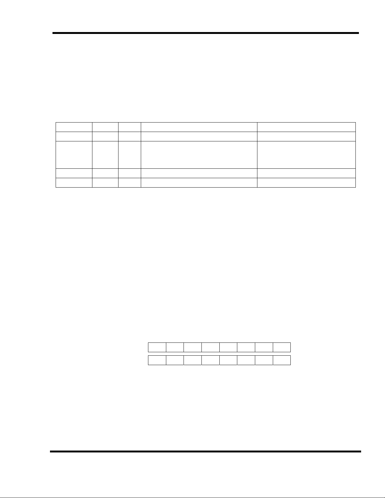
V9938 has 4 ports: port #0 – port #3; port number is selected by VDP address lines
A0 and A1. Table below also shows port address allocation for MSX compatible machine.
A1 A0 Operation Primary MSX port (Hex)
Port #0 0 0 VRAM Data (R/W) 98h
Port #1 0 1 Status Register (R)
VRAM Address (W)
Register set-up (W)
Port #2 1 0 Palette registers (W) 9Ah
Port #3 1 1 Register indirect addressing (W) 9Bh
There are two ways to set data in the MSX-VIDEO control registers (R#0 to R#46).
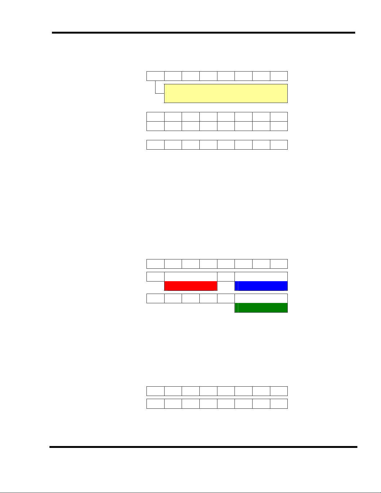
1.1.1. Direct access to VDP registers
Output the data and the register number in sequence to port #1. The order of reads
and writes to/from VDP ports is vitally important, thus you should keep in mind that this
order can be potentially interrupted by CPU interrupt routine which can write to or read
from VDP port(s) and thus break the proper sequence. In case of Z80 CPU, use DI
(disable interrupts) at the start and EI (enable interrupts) at the end of VDP your access
code.
Data byte is written first (bits D0-D7), and register number is written next to data
byte (bits R0-R5). If interrupt involving VDP operations will occur between these two
operations, it may cause unpredictable results.
MSB 7 6 5 4 3 2 1 0 LSB
Port #1 first byte D7 D6 D5 D4 D3 D2 D1 D0 Data
Port #1 second byte 1 0 R5 R4 R3 R2 R1 R0 Register #
1.1.2. Indirect access to registers through R#17 (Control Register Pointer)
Set the register number in R#17 using direct addressing and then send data to Port
#3. MSB of the value written to R#17 (AII) controls auto-incrementing of the register
number. If auto-incrementing is enabled, after each data read or write control register
pointer is incremented; if auto-incrementing is disabled then pointer value in R#17 remains
unchanged. Auto-increment mode is useful for bulk read or update of VDP registers.
99h
© 1985 ASCII CORP. / NIPPON GAKKI CO.
Page 13 of 108
© 2010-2015 Eugeny Brychkov
Note: data in register R#17 can not be changed by indirect addressing.
MSB 7 6 5 4 3 2 1 0 LSB
Register #17 AII 0 R5 R4 R3 R2 R1 R0 Register #
0: Auto-increment is enabled
1: Auto-increment is disabled
Port #3 first byte D7 D6 D5 D4 D3 D2 D1 D0 Data
Port #3 second byte D7 D6 D5 D4 D3 D2 D1 D0 Data
…
Port #3 nth byte D7 D6 D5 D4 D3 D2 D1 D0 Data
1.2. Accessing the Palette Registers
To set data in the MSX-VIDEO palette registers (P#0 to P#15) you must first set the
palette register number in register R#16 (Color palette address pointer) and subsequently
write two bytes of data (in specific order) into port #2. Every color consists of 3 sets of 3
bits: red, green and blue component (value 0…7).
Note: after writing pair of data to port #2 palette register number (pointer) in
register R#16 auto-increments.
MSB 7 6 5 4 3 2 1 0 LSB
Register #16 0 0 0 0 C3 C2 C1 C0 Palette #
Port #2 first byte 0 R2 R1 R0 0 B2 B1 B0 Data 1
Red data Blue data
Port #2 second byte 0 0 0 0 0 G2 G1 G0 Data 2
Green data
1.3. Accessing the status registers
To read the status registers of MSX-VIDEO (S#0 to S#9) you must first set the
register number in R#15 (Status register pointer) and then read data from port #1.
MSB 7 6 5 4 3 2 1 0 LSB
Register #15 (write) 0 0 0 0 S3 S2 S1 S0 Stat Reg #
Port #1 data (read) D7 D6 D5 D4 D3 D2 D1 D0 Data read
© 1985 ASCII CORP. / NIPPON GAKKI CO.
Page 14 of 108
© 2010-2015 Eugeny Brychkov

1.4. Accessing the Video RAM (VRAM)
A video RAM of 128K bytes plus an expansion RAM of 64K bytes can be attached to
the VDP. Memory map is shown below.
Address
1FFFFh
↑
↑
↑
↑
0FFFFh
10000h
↑
↑
↑
↑
Video RAM
(used for display)
00000h
Expansion RAM
(for data I/O
registers)
To access memory, use the following procedure:
1. Switch respective bank (VRAM or expansion RAM)
2. Set the address counter A16 to A14
3. Set the address counter A7 to A0
4. Set the address counter A13 to A8, and specify if following data command will be
read or write
5. Read or write data to the memory
Step 1: Switching banks (VRAM to expansion RAM)
Applications are used to work with Video RAM, thus re-specification of the bank is
rarely necessary. It will be required if your application will need to access expansion RAM.
After performing necessary operations on expansion RAM, ensure that you map the Video
RAM back.
MSB 7 6 5 4 3 2 1 0 LSB
Register #45 0 MXC MXD MXS DIY DIX EQ MAJ
0: Video RAM
1: Expansion RAM
Argument
register
(ARG)
© 1985 ASCII CORP. / NIPPON GAKKI CO.
Page 15 of 108
© 2010-2015 Eugeny Brychkov

Step 2: Setting the address counter A16 to A14
VDP can logically address 128K bytes in the address range of 00000h-1FFFFh through
16 address bits A16…A0. At this step we set up bits A16…A14 writing them into register
R#14 (VRAM access base address register).
MSB 7 6 5 4 3 2 1 0 LSB
Register #14 0 0 0 0 0 A16 A15 A14 Base reg
Step 3: Setting the address counter A7 to A0
Set the low-order eight bits A7…A0 of the address counter by writing data to port #1.
MSB 7 6 5 4 3 2 1 0 LSB
Port #1 A7 A6 A5 A4 A3 A2 A1 A0 A7…A0
Step 4: Setting the address counter A13 to A8 and operation mode
Set the remaining six bits A13…A8 of the address counter by writing data to the port
#1.
You also should specify which memory operation will follow – read or write. It is very
important, as if you specify that next operation will be a “read”, VDP will pre-fetch value
from the memory (specified by the address set up earlier) and will get ready for CPU data
read. If you will not do so and issue read command, VDP may not get enough timeslot to
read data from the VRAM and CPU may get invalid data.
If you specify that next command will be a “write”, then VDP does not do pre-fetch
and waits for write instead.
MSB 7 6 5 4 3 2 1 0 LSB
Port #1 0 W A13 A12 A11 A10 A9 A8
A13…A8
0: Next command is “Data Read”
1: Next command is “Data Write”
Step 5: Reading or writing data to memory
It is important to know that after every data read or data write operation from port
#0 address counter is being incremented. It is very useful when you need to read from or
write to the memory in sequential manner. However you should mind the timing, ensuring
that VDP has enough time to write cached data or read requested data. Please refer to the
data sheet for timings.
MSB 7 6 5 4 3 2 1 0 LSB
Port #0 D7 D6 D5 D4 D3 D2 D1 D0
Data
Addr ++
© 1985 ASCII CORP. / NIPPON GAKKI CO.
Page 16 of 108
© 2010-2015 Eugeny Brychkov

2. REGISTER FUNCTIONS
2.1. Control registers #0 to #23
#32 to #46
2.1.1. Mode registers
MSB 7 6 5 4 3 2 1 0 LSB
R#0 0 DG IE2 IE1 M5 M4 M3 0 Mode R#0
R#1 0 BL IE0 M1 M2 0 SI MAG Mode R#1
R#8 MS LP TP CB VR 0 SPD BW Mode R#8
R#9 LN 0 S1 S0 IL E0 *NT DC Mode R#9
* Indicates negative logic
R#0
DG
Digitize mode:
IE2 Enables interrupts from Light pen
IE1 Enables interrupt from horizontal retrace
M5 Screen mode flag (see Screen Modes chapter)
M4 Screen mode flag (see Screen Modes chapter)
R#1
M3 Screen mode flag (see Screen Modes chapter)
BL Blank screen: if set to 1, screen display is enabled. If set to 0, screen
display is disabled and no VRAM read operations are performed.
IE0 Enables interrupt from vertical retrace
M1 Screen mode flag (see Screen Modes chapter)
M2 Screen mode flag (see Screen Modes chapter)
SI
Sprite size:
8*8
R#8
MAG
MS
Sprite enlarging:
Mouse:
mouse. If set to 1, sets color bus into output mode and disables mouse
LP
Light pen:
TP Sets the color of code 0 to the color of the palette
CB
Color bus:
color bus into output mode
VR Selects the type and organization of VRAM. If set to 1, VRAM is 64Kx1Bit
or 64Kx4bits. If set to 0, VRAM is 16Kx1Bit or 16Kx4Bits. Affects how VDP
performs refresh on DRAM chips
SPD
Sprite disable:
are not performed.
BW Black/White: if set to 1, output is grayscale in 32 tones
when set to 1, sets the color bus into input mode and enables
sets the color bus to the input or output mode
when set to 1, sprite size is 16*16. If set to 0, sprite size is
If set to 1, sprites are enlarged (double size)
when set to 1, enables light pen
when set to 1, sets color bus into input mode. If set to 0, sets
if set to 1, sprites are not displayed and related VRAM reads
© 1985 ASCII CORP. / NIPPON GAKKI CO.
Page 17 of 108
© 2010-2015 Eugeny Brychkov
R#9
LN
Line:
if set to 1, vertical dot count is set to 212. If set to 0, vertical dot
count is 192
S1 Selects simultaneous mode
S0 Selects simultaneous mode
IL
EO
Interlace:
if set to 1, interlace; if set to 0, non-interlace mode
Even/Odd screens:
When set to 1, displays two graphic screens
interchangeably by even/odd field; if set to 0, displays same graphic
screen by even/odd field
*NT (RGB output only) If set to 1, PAL mode (313 lines, 50Hz); if set to 0,
NTSC mode (262 lines, 60Hz)
DC
Dot clock:
If set to 1, *DLCLK is in input mode; if set to 0, *DLCKL is in
output mode
2.1.2. Table Base address registers
When displaying information on the screen, VDP uses color, pattern, sprite and other
information from video RAM. It is important to set proper starting addresses of such VRAM
locations by writing to specified table base address registers.
Note: you should ensure that unused bits are set to 0. Further in the book bit set to
“0” will mean that this bit has to be set to 0, “1” will mean that this bit has to be set to 1,
and “*” will mean that value of the bit does not matter.
MSB 7 6 5 4 3 2 1 0 LSB
R#2 0 A16 A15 A14 A13 A12 A11 A10
Pattern layout
table
R#3 A13 A12 A11 A10 A9 A8 A7 A6 Color table low
R#10 0 0 0 0 0 A16 A15 A14 Color table high
R#4 0 0 A16 A15 A14 A13 A12 A11
R#5 A14 A13 A12 A11 A10 A9 A8 A7
R#11 0 0 0 0 0 0 A16 A15
R#6 0 0 A16 A15 A14 A13 A12 A11
Pattern
generator table
Sprite attribute
table low
Sprite attribute
table high
Sprite pattern
generator table
© 1985 ASCII CORP. / NIPPON GAKKI CO.
Page 18 of 108
© 2010-2015 Eugeny Brychkov
2.1.3. Color registers
Color registers are used to control MSX-VIDEO text and background screen colors,
blinking and other functions.
MSB 7 6 5 4 3 2 1 0 LSB
R#7 TC3 TC2 TC1 TC0 BD3 BD2 BD1 BD0
Text color in TEXT1 and
TEXT2 modes
Screen margin /
backdrop color
Text and screen
margin color
MSB 7 6 5 4 3 2 1 0 LSB
R#12 T23 T22 T21 T20 BC3 BC2 BC1 BC0
Color part 1 Color part 0
Text and
background
blink color
In TEXT2 mode, if attributes for blinking are set, color set in this register R#12 and in
register R#7 are displayed alternatively (blinked).
MSB 7 6 5 4 3 2 1 0 LSB
R#13 ON3 ON2 ON1 ON0 OF3 OF2 OF1 OF0
Display time for even
page
Display time for odd
page
Blinking period
register
In the TEXT2 mode and in bit map modes of GRAPHIC4 to GRAPHIC7 two pages can
be alternatively displayed (blinked). Write to this register R#13 in order for blinking to start.
MSB 7 6 5 4 3 2 1 0 LSB
R#20 0 0 0 0 0 0 0 0
R#21 0 0 1 1 1 0 1 1
R#22 0 0 0 0 0 1 0 1
Color burst
register 1
Color burst
register 2
Color burst
register 3
The above values of color burst registers are preset on power-on. If all the bits in all
three registers are set to 0, color burst of the composite video is not performed. If values
are returned to above values, VDP will start generating normal color burst signal.
© 1985 ASCII CORP. / NIPPON GAKKI CO.
Page 19 of 108
© 2010-2015 Eugeny Brychkov
2.1.4. Display registers
The display registers are used to control display position on the screen.
MSB 7 6 5 4 3 2 1 0 LSB
R#18 V3 V2 V1 V0 H3 H2 H1 H0
Display adjust
register
Register #18 controls horizontal and vertical alignment on the screen. Please refer to
the table below.
Value
7 … 1 0 15 … 8
H Left … … Center … … Right
V Top … … Center … .. Bottom
MSB 7 6 5 4 3 2 1 0 LSB
R#23 DO7 DO6 DO5 DO4 DO3 DO2 DO1 DO0
Vertical offset
register
This register R#23 sets the value of the first line to display on the screen. Virtual
screen size is 256 lines, visible vertical screen size can be 192 or 212 depending on LN bit
of register R#9. Setting R#23 to value other than 0 may display un-initialized parts of the
memory which may look as garbage. Display of virtual screen is performed in cycle,
meaning that when increasing value of R#23 top of virtual screen appears at the bottom of
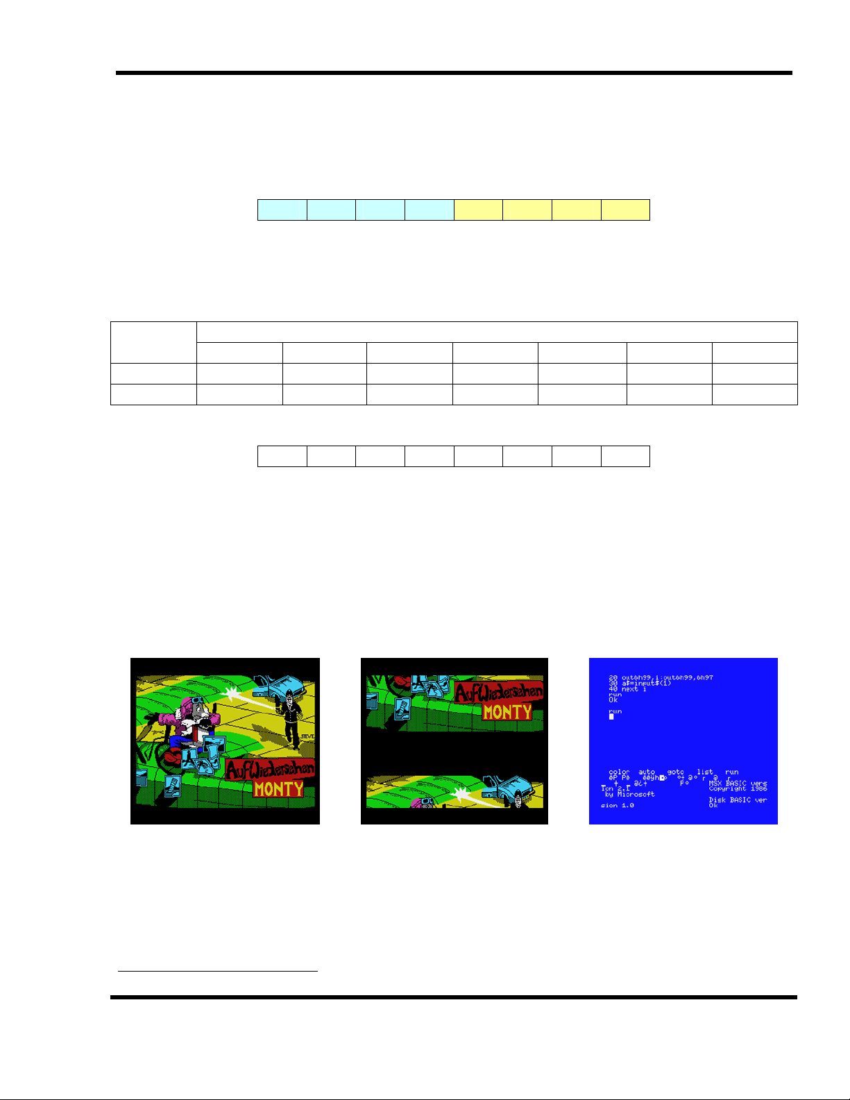
visible screen. Please see pictures below.
Original screen* in
GRAPHIC1 mode
Offset screen*, horizontal
scan line is 256 dots,
GRAPHIC1 mode, top
appears at the bottom
TEXT1 mode, horizontal
scan line is 240 dots,
garbage in un-initialized
memory space
* “Auf Wiedersehen Monty” image, a property of Gremlin Graphics. Used in this book for educational purposes only
© 1985 ASCII CORP. / NIPPON GAKKI CO.
Page 20 of 108
© 2010-2015 Eugeny Brychkov

MSB 7 6 5 4 3 2 1 0 LSB
R#19 IL7 IL6 IL5 IL4 IL3 IL2 IL1 IL0
Interrupt line
register
VDP generates interrupt when it starts to display respective scan line if bit 4 “IE1” of
register R#0 is set to 1. Write a value to this register R#19, and when VDP will start
displaying the specified line, it will set bit 0 “FH” of status register S#1 to 1.
2.1.5. Access registers
Access registers is the set of registers used for accessing other VDP registers or VRAM.
These registers include R#14, R#15, R#16 and R#17.
MSB 7 6 5 4 3 2 1 0 LSB
R#14 0 0 0 0 0 A16 A15 A14
VRAM access
base register
R#14 contains three senior bits of VRAM access address. In all modes, except
GRAPHIC1, GRAPHIC2, MULTICOLOR and TEXT1, if there’s a carry flag from A13 the value
in this register is automatically incremented.
MSB 7 6 5 4 3 2 1 0 LSB
R#15 0 0 0 0 S3 S2 S1 S0
Status register
pointer
R#15 points to the respective status register (S#0…S#9) to be read.
MSB 7 6 5 4 3 2 1 0 LSB
R#16 0 0 0 0 C3 C2 C1 C0
Color palette
address register
R#16 points to the respective color palette register (P#0…P#15) to be accessed.
MSB 7 6 5 4 3 2 1 0 LSB
R#17 AII 0 RS5 RS4 RS3 RS2 RS1 RS0
Control register
pointer
R#17 is a register used in indirect access to other VDP registers. It also has autoincrement flag (AII) which is used to control increment of value in this register.
© 1985 ASCII CORP. / NIPPON GAKKI CO.
Page 21 of 108
© 2010-2015 Eugeny Brychkov
2.1.6. Command registers
The following command registers are used when executing a command on the MSXVIDEO. Details on the use of these command registers will be presented in later chapter.
MSB 7 6 5 4 3 2 1 0 LSB
R#32 SX7 SX6 SX5 SX4 SX3 SX2 SX1 SX0
R#33 0 0 0 0 0 0 0 SX8
R#34 SY7 SY6 SY5 SY4 SY3 SY2 SY1 SY0
R#35 0 0 0 0 0 0 SY9 SY8
Source X low
register
Source X high
register
Source Y low
register
Source Y high
register
MSB 7 6 5 4 3 2 1 0 LSB
R#36 DX7 DX6 DX5 DX4 DX3 DX2 DX1 DX0
R#37 0 0 0 0 0 0 0 DX8
R#38 DY7 DY6 DY5 DY4 DY3 DY2 DY1 DY0
R#39 0 0 0 0 0 0 DY9 DY8
Destination X
low register
Destination X
high register
Destination Y
low register
Destination Y
high register
MSB 7 6 5 4 3 2 1 0 LSB
R#40 NX7 NX6 NX5 NX4 NX3 NX2 NX1 NX0
R#41 0 0 0 0 0 0 0 NX8
R#42 NY7 NY6 NY5 NY4 NY3 NY2 NY1 NY0
R#43 0 0 0 0 0 0 NY9 NY8
Number of dots
X low register
Number of dots
X high register
Number of dots
Y low register
Number of dots
Y high register
MSB 7 6 5 4 3 2 1 0 LSB
R#44 CH3 CH2 CH1 CH0 CL3 CL2 CL1 CL0
R#45 0 MXC MXD MXS DIY DIX EQ MAJ
R#46 CM3 CM2 CM1 CM0 LO3 LO2 LO1 LO0
Color register
Argument
register
Command
register
© 1985 ASCII CORP. / NIPPON GAKKI CO.
Page 22 of 108
© 2010-2015 Eugeny Brychkov
2.2. Status registers #0 to #9
The following status registers are read-only registers for VDP status reporting. Let’s
consider each register.
MSB 7 6 5 4 3 2 1 0 LSB
S#0 F 5S C 5SN Status register 0
7 F
6 5S
5 C
4…0 5SN The number of 5
S#1 FL LPS ID # FH Status register 1
7 FL
6 LPS
5…1 ID # The identification number of the VDP chip
0 FH
S#2 TR VR HR BD 1 1 EO CE Status register 2
7 TR
6 VR
5 HR
4 BD
1 EO
0 CE
Vertical scan interrupt flag.
Flag for 5th sprite.
Five (or nine in G3…G7 modes) sprites are aligned on
When S#0 is read, this flag is reset
the same horizontal line
Collision flag.
Two sprites have collided
th
(or 9th in G3…G7 modes) sprite
MSB 7 6 5 4 3 2 1 0 LSB
Light pen.
Is set if light pen detects light. If IE2 is set, interrupt is
generated. Reset when S#1 is read.
Mouse 2.
Is set if second button of mouse was pressed. This flag is not
reset when reading status register S#1
Light pen button.
Mouse 1.
Is set if first button of mouse was pressed
Is set when light pen button is pressed
This flag is not reset when reading status register S#1 in both set-ups
Horizontal scan interrupt flag.
Is set if VDP scans line specified in register
R#19. If IE1 is set, interrupt is generated. FH is reset when S#1 is read
MSB 7 6 5 4 3 2 1 0 LSB
Transfer ready flag.
If set to 1, indicates to the CPU that VDP is ready for
next transfer. Value of 0 means that VDP is not ready
Vertical retrace flag.
Is set during scanning of VBLANK area of the screen,
i.e. during vertical retrace plus while lower and upper borders of the
screen is drawn
Horizontal retrace flag.
Is set during scanning of HBLANK area of the
screen, i.e. when right and left borders of the screen are drawn
Color detect flag.
When the search command is executed, this flag is set if
specified color was detected
Display field flag.
If set to 0, indicates the first field. If set to 1, indicated
the second field
Command execution flag.
If set to 1, indicates that VDP is busy executing
a command
© 1985 ASCII CORP. / NIPPON GAKKI CO.
Page 23 of 108
© 2010-2015 Eugeny Brychkov
MSB 7 6 5 4 3 2 1 0 LSB
S#3 X7 X6 X5 X4 X3 X2 X1 X0
S#4 1 1 1 1 1 1 1 X8
S#5 Y7 Y6 Y5 Y4 Y3 Y2 Y1 Y0
S#6 1 1 1 1 1 1 Y9 Y8
Column register
low
Column register
high
Row register
low
Row register
high
The above registers S#3…S#6 contain coordinate information about collision location
of the sprites, or location of light pen, or relative movement of the mouse.
MSB 7 6 5 4 3 2 1 0 LSB
S#7 C7 C6 C5 C4 C3 C2 C1 C0 Color register
This color register is used when executing commands “POINT” and “VRAM to CPU”
and contains VRAM data.
MSB 7 6 5 4 3 2 1 0 LSB
S#8 BX7 BX6 BX5 BX4 BX3 BX2 BX1 BX0
S#9 1 1 1 1 1 1 1 BX8
Coded color X
register low
Coded color X
register high
When the search command is executed and coded color had been detected (see R#2),
this register contains its X coordinate.
© 1985 ASCII CORP. / NIPPON GAKKI CO.
Page 24 of 108
© 2010-2015 Eugeny Brychkov
3. SCREEN MODES
3.1. TEXT1 mode
Characteristics
Pattern size (w*h) 6 dots * 8 dots
Patterns 256 types
Screen size (w*h) 40 * 24 patterns
Pattern colors Two colors out of 512 (per screen)
VRAM area per screen 4K bytes
Controls
Pattern font VRAM pattern generator table
Screen pattern location VRAM pattern name table
Pattern color code 1 High-order four bits of R#7
Pattern color code 0 Low-order four bits of R#7
Background color code Low-order four bits of R#7
Mode flags
Bit M5 (R#0) M4 (R#0) M3 (R#0) M2 (R#1) M1 (R#1)
Value 0 0 0 0 1
MSX system default values
BASIC SCREEN number Pattern generator Pattern layout
0, width 1 … 40 00800h … 00FFFh 00000h … 003BFh
© 1985 ASCII CORP. / NIPPON GAKKI CO.
Page 25 of 108
© 2010-2015 Eugeny Brychkov
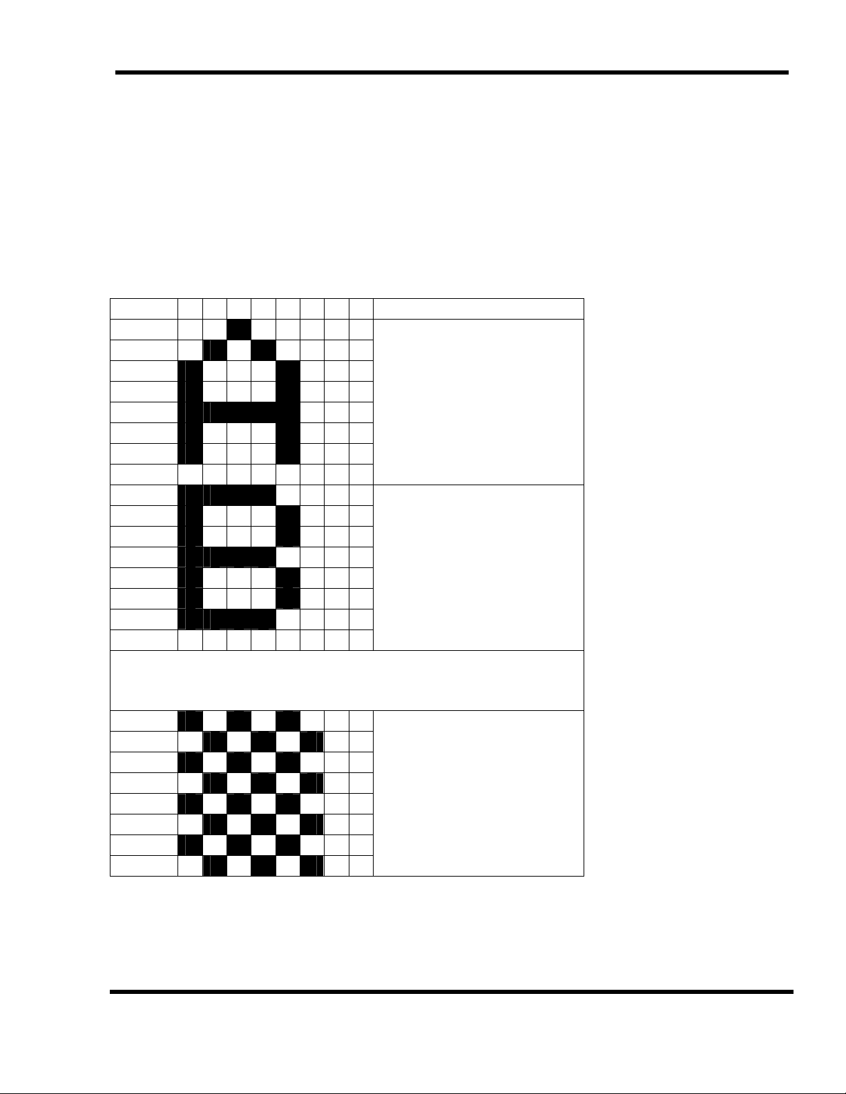
3.1.2. Pattern Generator Table
The pattern generator table is a location in VRAM that stores patterns (font). Each
pattern has number from PN0 to PN255. The font displayed on the screen for each pattern
is constructed from 8 bytes, with 6 high-order bits displayed and 2 low-order bits not
displayed. Pattern generator table base is stored in the register R#4.
Example of pattern generator table is provided below.
MSB LSB
Offset 7 6 5 4 3 2 1 0
0
1
2
3
Pattern number o (PN0)
4
5
6
7
8
9
10
11
Pattern number 1 (PN1)
12
13
14
15
● ● ●
● ● ●
● ● ●
2040
2041
2042
2043
2044
Pattern number 255
(PN255)
2045
2046
2047
© 1985 ASCII CORP. / NIPPON GAKKI CO.
Page 26 of 108
© 2010-2015 Eugeny Brychkov

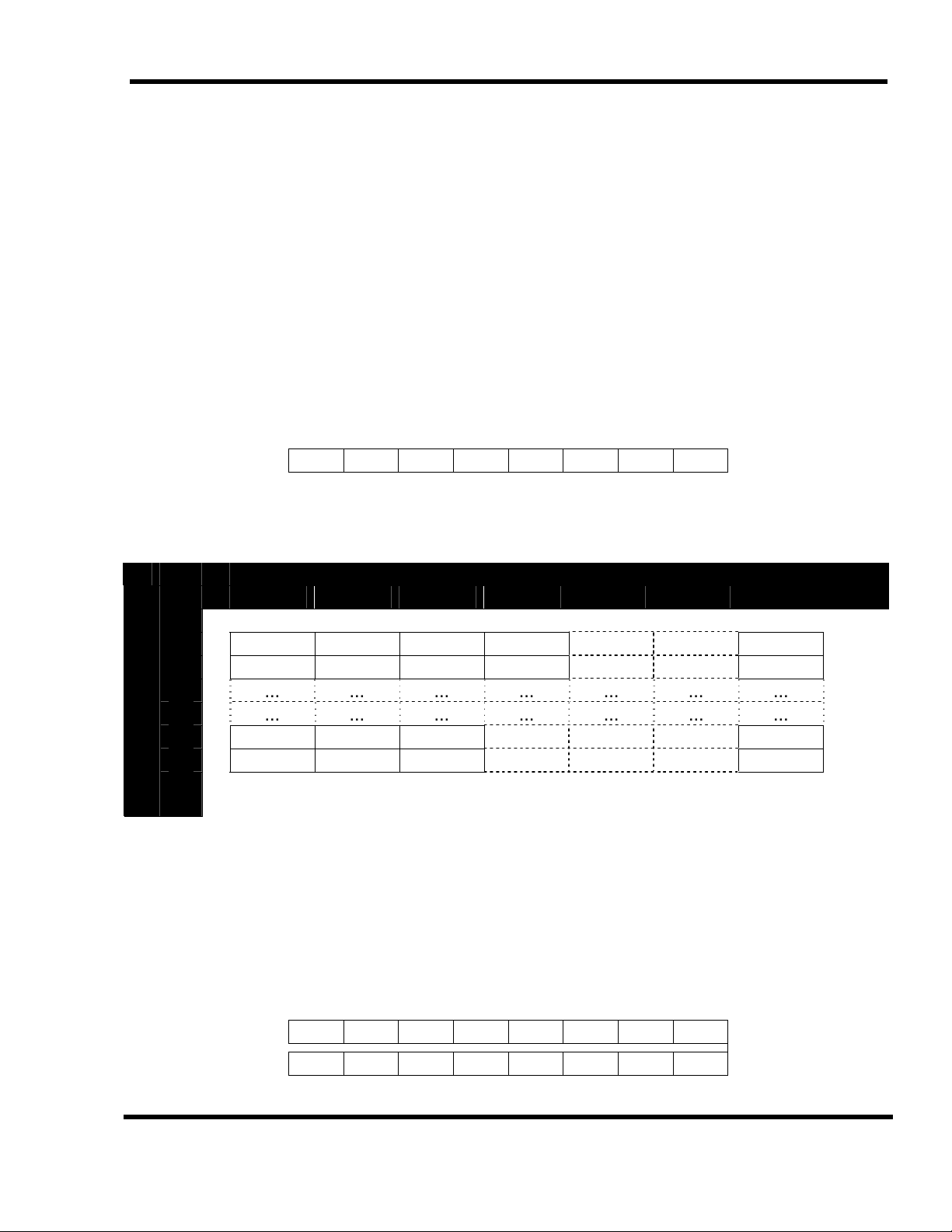
3.1.3. Pattern Layout Table settings
The pattern layout table is a map of the screen (per screen image). Every location of
the screen contains code of the pattern displayed at respective location. This table has
40*24 (960) locations where defined patterns can be displayed. Pattern layout table base
address is stored in register R#2, and corresponds to the cell (0, 0) with address 0 in the
picture below.
Columns
0 1 2 3 39
← X
0 0 1 2 3 … … 39
1 40 41 42 43 … … 79
… … … … … … …
… … … … … … …
Rows
22 880 881 882 … … … 919
23 920 921 922 … … … 959
↑
Y
3.1.4. Color register settings
Color settings are located in the register R#7. Bits TC3…TC0 specify pattern color
code of the pixels identified as “1” in the bitmap values of pattern generator table, bits
BD3…BD0 specify pattern color code of the pixels identified as “0” in the bitmap values of
pattern generator table as well as screen border color.
Note: screen border color is the same as the pattern backdrop color in TEXT1 mode.
© 1985 ASCII CORP. / NIPPON GAKKI CO.
Page 27 of 108
© 2010-2015 Eugeny Brychkov

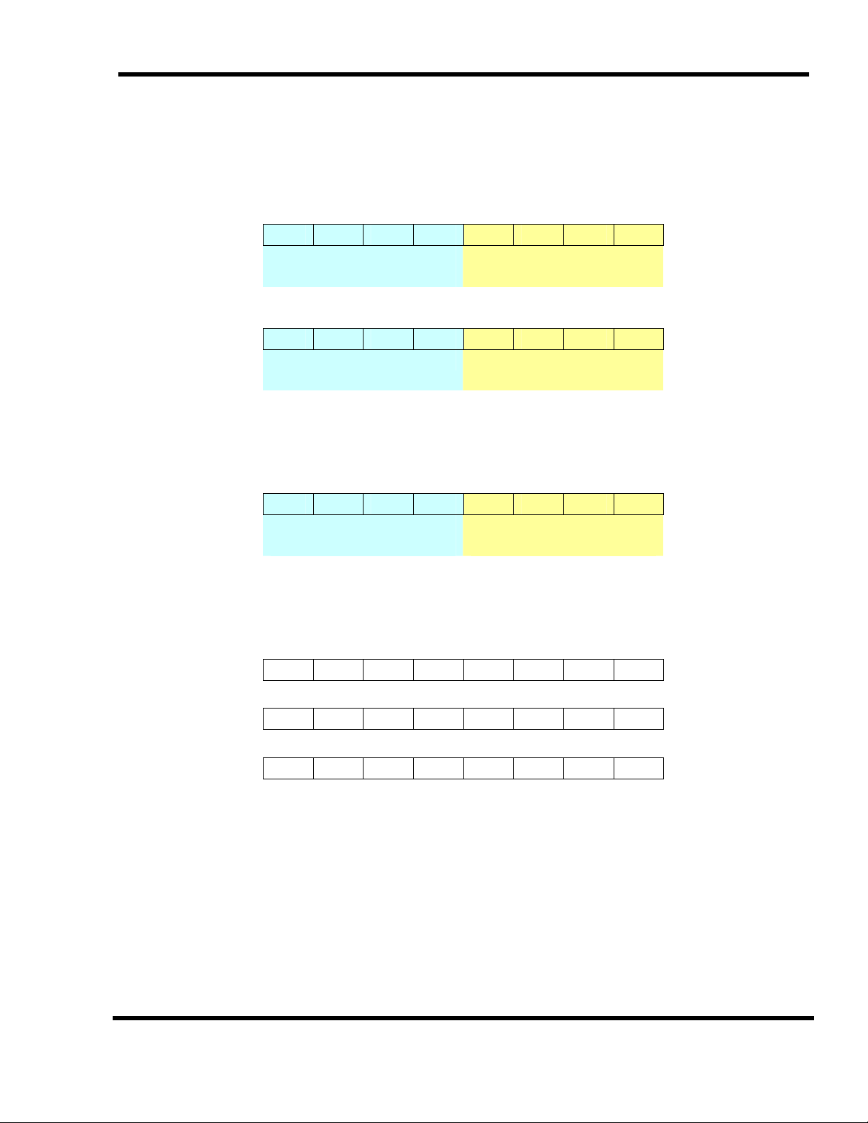
3.1.5. Example of VRAM allocation for TEXT1 mode
00000h
003BFh
00800h
00FFFh
01000h
Pattern layout
table 0
Pattern generator
table 0
Pattern layout
table 1
MSB 7 6 5 4 3 2 1 0 LSB
R#2 0 0 0 0 0
A16 A15 A14 A13
MSB 7 6 5 4 3
R#4 0 0 0 0 0 0 0 1
A16 A15 A14 A13 A12 A11
MSB 7 6 5 4 3
R#2 0 0 0 0 0
A16 A15 A14 A13 A12 A11 A10
013BFh
MSB 7 6 5 4 3
R#4 0 0 0 0 0 0 1 1
A16 A15 A14 A13 A12 A11
01800h
Pattern generator
table 1
01FFFh
1FFFFh
Maximum of 32 pages may be allocated in the same
manner if VDP has 128K bytes attached to it.
0 0 0
A12 A11 A10
2 1 0 LSB
2 1 0 LSB
1 0 0
2 1 0 LSB
© 1985 ASCII CORP. / NIPPON GAKKI CO.
Page 28 of 108
© 2010-2015 Eugeny Brychkov

3.2. TEXT2 mode
Characteristics
Pattern size (w*h) 6 dots * 8 dots
Patterns 256 types
Screen size (w*h) 80 * 24 patterns if LN bit of R#9 set to 0
80 * 26.5 patterns if LN bit of R#9 set to 1
Pattern colors Two colors out of 512 (per screen), four if using blinking
VRAM area per screen 8K bytes
Controls
Pattern font VRAM pattern generator table
Screen pattern location VRAM pattern name table
Pattern color code 1 High-order four bits of R#7
Pattern color code 0 Low-order four bits of R#7
Background color code Low-order four bits of R#7
Blinking pattern color
code 1
Blinking pattern color
code 0
Mode flags
Bit M5 (R#0) M4 (R#0) M3 (R#0) M2 (R#1) M1 (R#1)
Value 0 1 0 0 1
Other flags
LN bit of R#9 0: 24 lines displayed
MSX system default values
BASIC SCREEN number Pattern generator Pattern layout Pattern color table
0, width 41 … 80 01000h … 017FFh 00000h … 0077Fh
High-order four bits of R#12
Low-order four bits of R#12
1: 26.5 lines displayed
00000h … 0086Fh
00800h … 008EFh
00800h … 0090Dh
© 1985 ASCII CORP. / NIPPON GAKKI CO.
Page 29 of 108
© 2010-2015 Eugeny Brychkov
3.2.2. Pattern Generator Table
Organization of pattern generator table is the same as in TEXT1 mode. Register R#4
defines base address of the table.
3.2.3. Pattern layout table settings
The pattern layout table is a map of the screen (per screen image). Every location of
the screen contains code of the pattern displayed at respective location. This table has
80*27 (2160) locations where defined patterns can be displayed. Pattern layout table base
address is stored in register R#2 (see below), and corresponds to the cell (0, 0) with
address 0 in the picture below. Note that if LN bit of R#9 is set to 1, then 26 lines are
displayed, plus an upper half of 27th pattern line is displayed.
MSB 7 6 5 4 3 2 1 0 LSB
R#2 0 A16 A15 A14 A13 A12 1 1
Pattern layout
table
Screen mapping of pattern layout table is provided below.
Columns
0 1 2 3 79
← X
0 0 1 2 3 … … 79
1 80 81 82 83 … … 159
… … … … … … …
… … … … … … …
Rows
25 2000 2001 2002 … … … 2079
26 2080 2081 2082 … … … 2159
↑
Y
3.2.4. Color table settings
Each position on the screen has separate bit for the blinking attribute, and if this bits
is set to 1, blinking will be applied to the pattern placed in this area in the pattern layout
table. Table start address is set in registers R#3 and R#10.
MSB 7 6 5 4 3 2 1 0 LSB
R#3 A13 A12 A11 A10 A9 1 1 1
R#10 0 0 0 0 0 A16 A15 A14
Color table base
address
registers
© 1985 ASCII CORP. / NIPPON GAKKI CO.
Page 30 of 108
© 2010-2015 Eugeny Brychkov
 Loading...