

このサービスマニュアルはエコパルプ
(ECF:無塩素系漂白パルプ)を使用しています。
This document is printed on chlorine free (ECF) paper.
SERVICE MANUAL
■ CONTENTS (目次)
SPECIFICATIONS (総合仕様)..................................................................... 4
DIMENSIONS (寸法図).............................................................................. 7
PANEL LAYOUT (パネルレイアウト)......................................................... 8
CIRCUIT BOARD LAYOUT (ユニットレイアウト).................................... 9
DISASSEMBLY PROCEDURES (分解手順)............................................. 10
LSI PIN DESCRIPTION (LSI端子機能表).................................................. 17
IC BLOCK DIAGRAM (ICブロック図)...................................................... 23
CIRCUIT BOARDS (シート基板図)........................................................... 26
TEST PROGRAM (テストプログラム)................................................ 36/45
INSPECTIONS (検査).......................................................................... 54/57
UPDATING PROGRAM, BOOT, AND COMPONENT DATA
(プログラム、ブート、コンポーネントデータのアップデート)......... 60/64
INITIALIZING (初期化)........................................................................ 68/69
SYSTEM FLOW CHART (電源立ち上げシーケンス).......................... 70/71
DISPLAY MESSAGES (ディスプレイメッセージ)............................. 72/74
OUTPUT LEVEL CHANGE METHOD (出力レベル変更方法).................. 76
PARTS LIST
LEVEL DIAGRAM (レベルダイアグラム)
BLOCK DIAGRAM (ブロックダイアグラム)
WIRING DIAGRAM (基板結線図)
CIRCUIT DIAGRAM (回路図)
PA 011826
SP2060: 20060720-249900
HAMAMATSU, JAPAN
Copyright (c) Yamaha Corporation. All rights reserved. 06.06
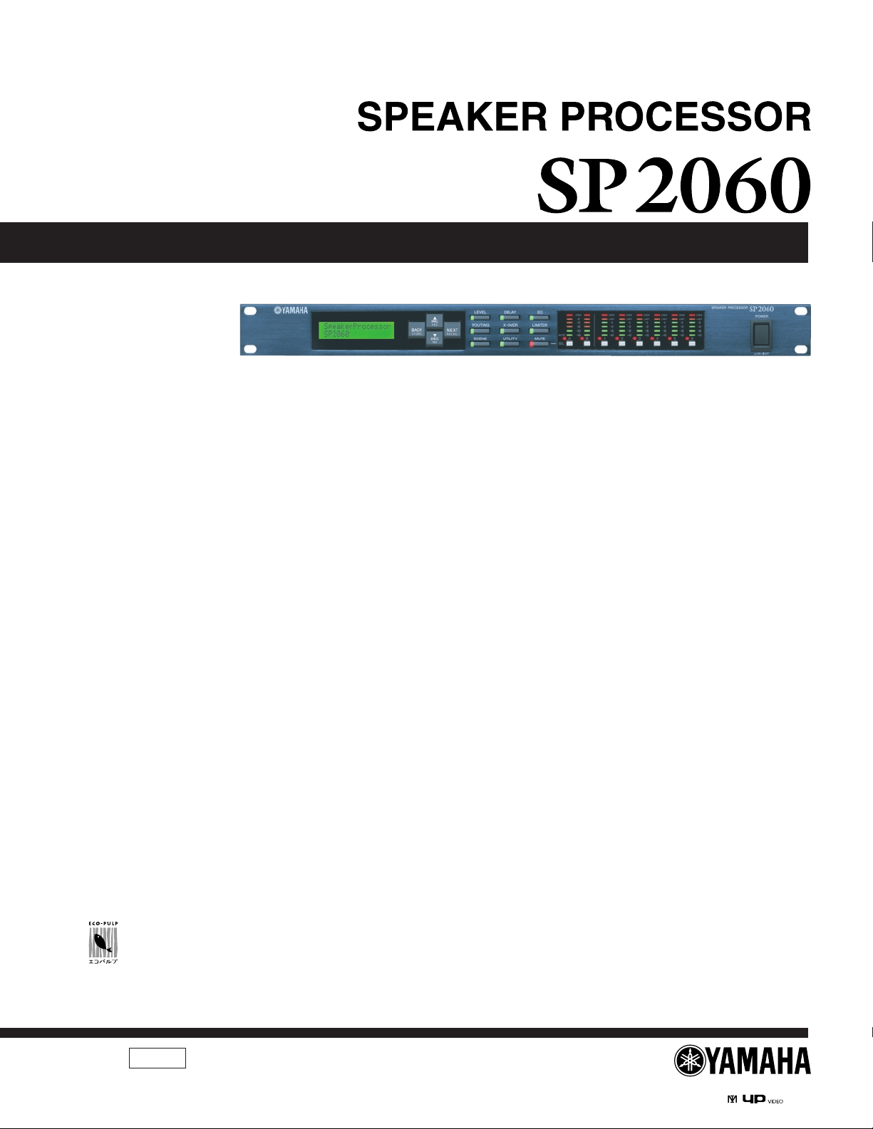
SP2060
IMPORTANT NOTICE
This manual has been provided for the use of authorized Yamaha Retailers and their service personnel. It has been assumed that basic service
procedures inherent to the industry, and more specifically Yamaha Products, are already known and understood by the users, and have
therefore not been restated.
WARNING: Failure to follow appropriate service and safety procedures when servicing this product may result in personal injury, destruc-
tion of expensive components and failure of the product to perform as specified. For these reasons, we advise all Yamaha
product owners that all service required should be performed by an authorized Yamaha Retailer or the appointed service
representative.
IMPORTANT: This presentation or sale of this manual to any individual or firm does not constitute authorization, certification, recognition of
any applicable technical capabilities, or establish a principal-agent relationship of any form.
The data provided is believed to be accurate and applicable to the unit(s) indicated on the cover. The research engineering, and service
departments of Yamaha are continually striving to improve Yamaha products. Modifications are, therefore, inevitable and changes in specification are subject to change without notice or obligation to retrofit. Should any discrepancy appear to exist, please contact the distributor’s Service
Division.
WARNING: Static discharges can destroy expensive components. Discharge any static electricity your body may have accumulated by
IMPORTANT: Turn the unit OFF during disassembly and parts replacement. Recheck all work before you apply power to the unit.
grounding yourself to the ground bus in the unit (heavy gauge black wires connect to this bus).
WARNING: CHEMICAL CONTENT NOTICE!
The solder used in the production of this product contains LEAD. In addition, other electrical/electronic and/or plastic (Where applicable)
components may also contain traces of chemicals found by the California Health and Welfare Agency (and possibly other entities) to cause
cancer and/or birth defects or other reproductive harm.
DO NOT PLACE SOLDER, ELECTRICAL/ELECTRONIC OR PLASTIC COMPONENTS IN YOUR MOUTH FOR ANY REASON WHAT SO
EVER!
Avoid prolonged, unprotected contact between solder and your skin! When soldering, do not inhale solder fumes or expose eyes to solder/flux
vapor!
If you come in contact with solder or components located inside the enclosure of this product, wash your hands before handling food.
IMPORTANT NOTICE FOR THE UNITED KINGDOM
Connecting the Plug and Cord
WARNING: THIS APPARATUS MUST BE EARTHED
IMPORTANT. The wires in this mains lead are coloured in accordance with the following code:
As the colours of the wires in the mains lead of this apparatus may not correspond with the coloured markings identifying the terminals in your
plug, proceed as follows:
The wire which is coloured GREEN and YELLOW must be connected to the terminal in the plug which is marked by the letter E or by the safety
earth symbol or colored GREEN or colored GREEN and YELLOW.
The wire which is coloured BLUE must be connected to the terminal which is marked with the letter N or coloured BLACK.
The wire which is coloured BROWN must be connected to the terminal which is marked with the letter L or coloured RED.
GREEN-AND-YELLOW: EARTH
BLUE: NEUTRAL
BROWN: LIVE
■ WARNING
Components having special characteristics are marked and must be replaced with parts having specification equal to those originally
installed.
印の部品は、安全を維持するために重要な部品です。交換する場合は、安全のために必ず指定の部品をご使用ください。
2

SP2060
LITHIUM BATTERY HANDLING
This product uses a lithium battery for memory back-up.
WARNING : Lithium batteries are dangerous because they can be exploded by improper handling. Observe the following
precautions when handling or replacing lithium batteries.
• Leave lithium battery replacement to qualified service personnel.
• Always replace with batteries of the same type.
• When installing on the PC board by soldering, solder using the connection terminals provided on the battery cells.
• Never solder directly to the cells. Perform the soldering as quickly as possible.
• Never reverse the battery polarities when installing.
• Do not short the batteries.
• Do not attempt to recharge these batteries.
• Do not disasemble the batteries.
• Never heat batteries or throw them into fire.
ADVARSEL!
Lithiumbatteri—Eksplosionsfare ved fejlagtig håndtering. Udskiftning må kun ske med batteri af samme fabrikat og type. Levér
det brugte batteri tilbage til leverandoren.
VARNING
Explosionsfara vid felaktigt batteribyte. Använd samma batterityp eller an ekvivalent typ som rekommenderas av apparattillverkaren.
Kassera använt batteri enligt fabrikantens instruktion.
VAROITUS
Paristo voi räjähtää, jos se on virheellisesti asennettu. Vaihda paristo ainoastaan laitevalmistajan suosittelemaan tyyppiin. Hävitä
käytetty paristo valmistajan ohjeiden mukaisesti.
The following information complies with Dutch official Gazette 1995. 45; ESSENTIALS OF ORDER ON THE COLLECTION OF
BATTERIES.
• Please refer to the diassembly procedure for the removal of Back-up Battery.
• Leest u voor het verwijderen van de backup batterij deze beschrijving.
リチウム電池の取り扱い
<注意>
● リチウム電池を誤って交換すると爆発する危険があります。交換する場合は、サービスマニュアルで指定された部品を使用してく
ださい。
■ SAVING DATA (データの保存)
When you exchange the CPU circuit board, the data stored in
the memory will be lost.
Before exchanging the CPU circuit board, save the data to an
external device (such as a computer) with the backup function
of the DME Designer (version 2.0 or later).
For more information on the saving operation, refer to the DME
Designer owner’s manual.
CPU基板を交換すると、メモリー内に保存されていた内容が失
われます。
基板交換の前に、DMEDesigner(バージョン2.0以上)のバック
アップ機能を使って、データをパソコンなどの外部機器に保存
してください。
操作方法の詳細は、DMEDesigner取扱説明書を参照してくだ
さい。
3
SP2060
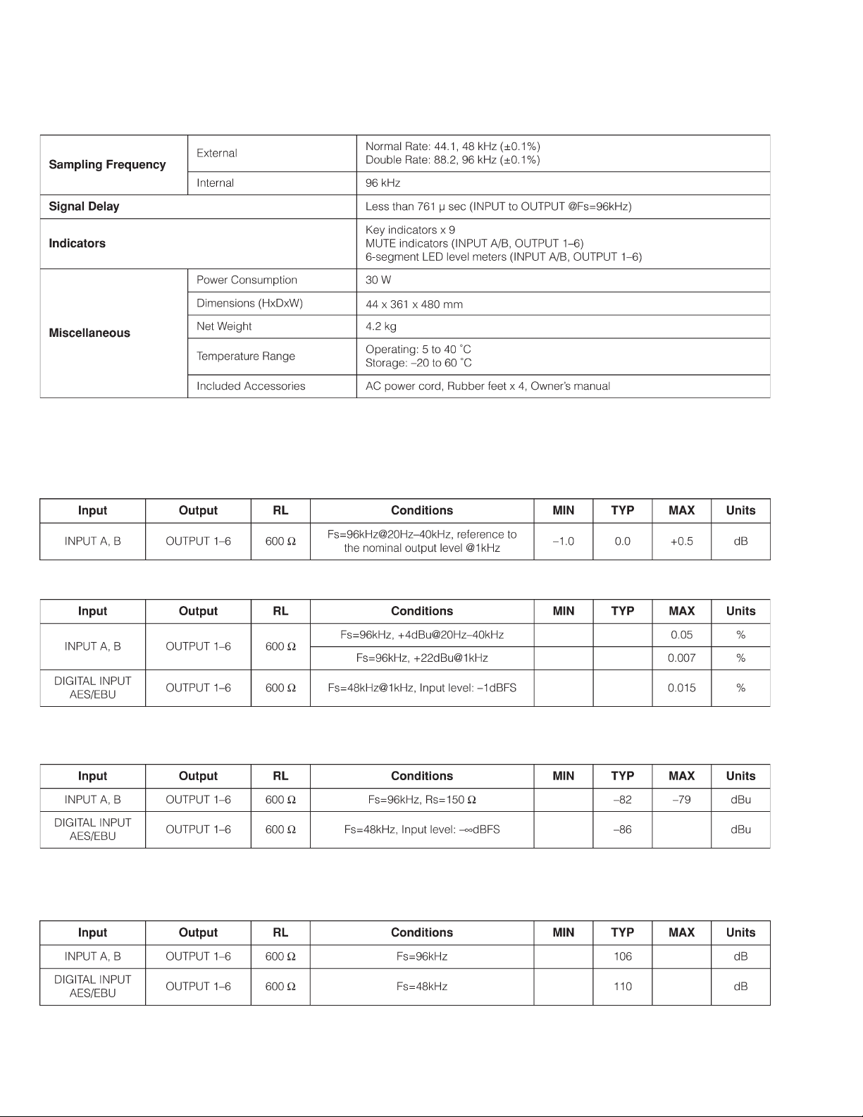
■ SPECIFICATIONS (総合仕様)
• General Specifications (一般仕様)
• Electrical Characteristics (電気的特性)
Output impedance of signal generator: 150 Ω
Frequency Response
Total Harmonic Distortion
* Total Harmonic Distortion is measured with a 18dB/octave filter @80kHz.
Hum & Noise
Dynamic Range
4
* Hum & Noise are measured with a 6dB/octave filter @12.7kHz; equivalent to a 20kHz filter with infinite dB/octave
attenuation.
* Dynamic range is measured with a 6dB/octave filter @12.7kHz; equivalent to a 20kHz filter with infinite dB/octave
attenuation.
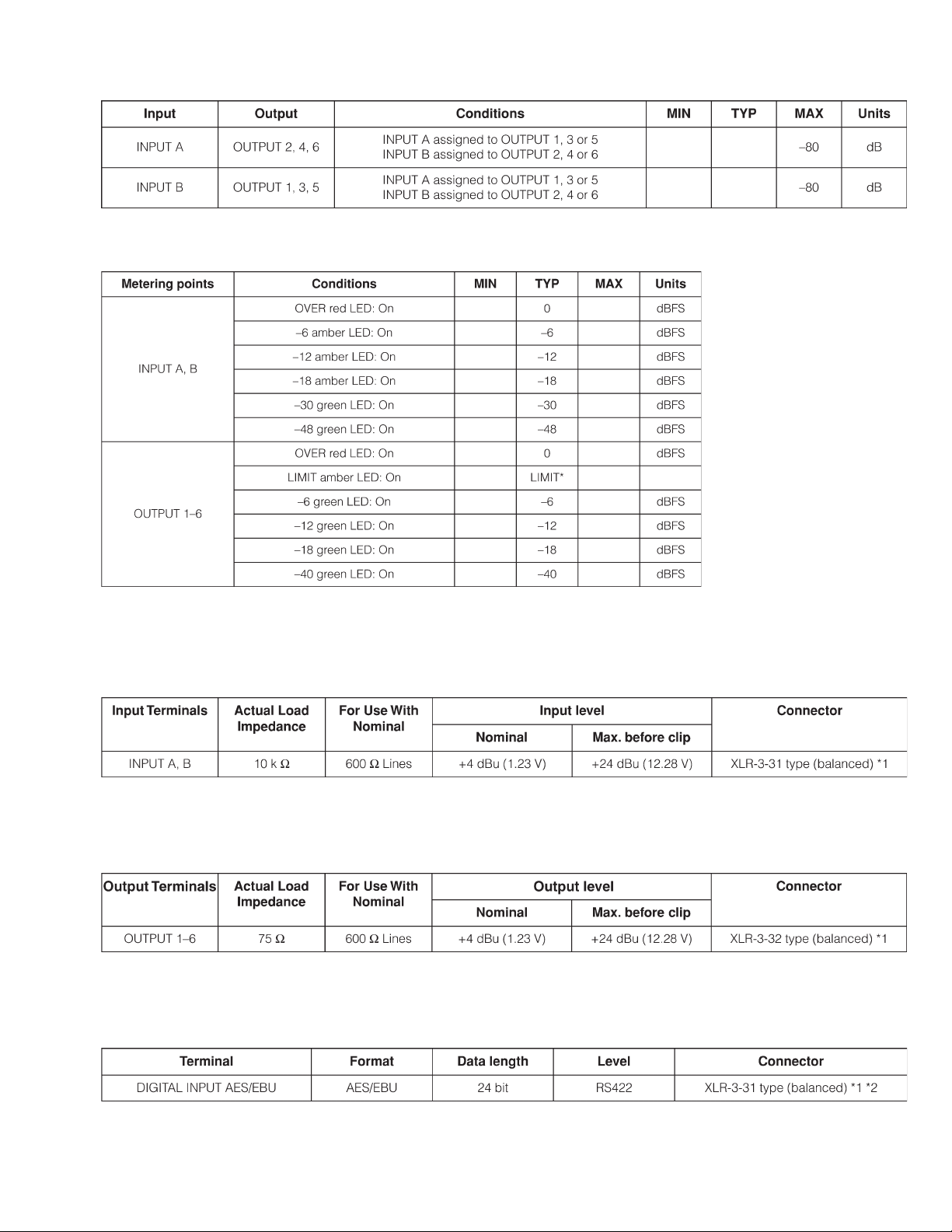
SP2060
Crosstalk @1KHz
LED Level Meters
Fs=96kHz
* Crosstalk is measured with a 18dB/octave filter @80kHz.
* The LED turns on when the internal limiter is activated.
• Input/Output Characteristics (入出力特性)
Analog Input Characteristics
*1.XLR-3-31 type connectors with latches are balanced. (1=GND, 2=HOT, 3=COLD)
*2.In these specifications, 0 dBu is referenced to 0.775 Vrms.
*3.All AD converters are 24-bit linear, 64-times oversampling. (Fs=96kHz)
Analog Output Characteristics
*1.XLR-3-32 type connectors are balanced. (1=GND, 2=HOT, 3=COLD)
*2.In these specifications, 0 dBu is referenced to 0.775 Vrms.
*3.All DA converters are 24-bit linear, 128-times oversampling (Fs=48kHz) or 64-times oversampling (Fs=96kHz).
Digital Input Characteristics
*1.XLR-3-31 type connector with latch is balanced. (1=GND, 2=HOT, 3=COLD)
*2.Only Double Speed Format is supported at 96 kHz. Double Channel or Single Format is not supported.
5
SP2060
Control I/O Characteristics
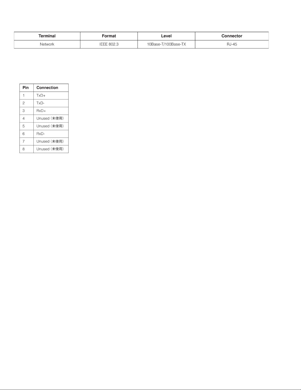
• Connector Pin Assignment (コネクターピンアサイン)
[NETWORK] Connector (100Base-TX Ethernet, RJ-45)
[NETWORK]端子(100Base-TXEthernet、RJ-45コネクター)
6
■ DIMENSIONS (寸法図)
361
SP2060
(4)
354
440
480
3
144
Unit: mm
単位:mm
7
SP2060
■ PANEL LAYOUT (パネルレイアウト)
• Front Panel (フロントパネル)
1 Display
2 [BACK/STORE] Key
3 [▲INC/YES]/[▼DEC/NO] Keys
4 [NEXT/RECALL] Key
5 [LEVEL] Key
6 [DELAY] Key
7 [EQ] Key
8 [ROUTING] Key
9 [X-OVER] Key
0 [LIMITER] Key
A [SCENE] Key
B [UTILITY] Key
C [MUTE] Key
D [SEL] Keys
E Meters
F [POWER ON/OFF] Key
2 4 5 6 731
YES
STORE RECALL
NO
8A9B0
E F
654321BA
C
1 ディスプレイ
2[BACK/STORE]キー
3[▲INC/YES]/[▼DEC/NO]キー
4[NEXT/RECALL]キー
5[LEVEL]キー
6[DELAY]キー
7[EQ]キー
8[ROUTING]キー
9[X-OVER]キー
0[LIMITER]キー
A[SCENE]キー
B[UTILITY]キー
C[MUTE]キー
D[SEL]キー
E メーター
F[POWERON/OFF]ボタン
D
• Rear Panel (リアパネル)
G H
G Ground Screw
H [AC IN] Connector
I [NETWORK] Connector
J [DIGITAL INPUT] Connector (AES/EBU)
K [OUTPUT] Connectors
L [INPUT] Connectors
8
I J K L
DIGITAL
INPUT
AES/EBU
G アース用ネジ
H[ACIN]端子
I[NETWORK]端子
J[DIGITALINPUT]端子(AES/EBU)
K[OUTPUT]端子
L[INPUT]端子
OUTPUT
123456
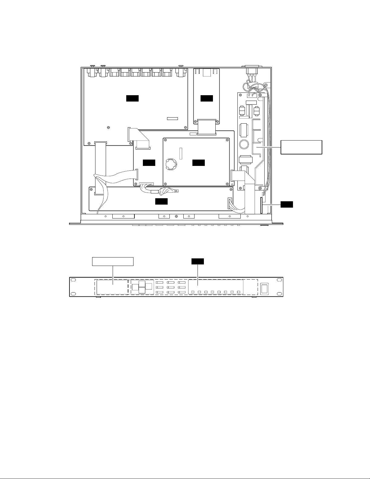
■ CIRCUIT BOARD LAYOUT (ユニットレイアウト)
ANA ENT
CPUDSP
SP2060
POWER SUPPLY
UNIT
LCD MODULE
DC
PS
PN
9
SP2060
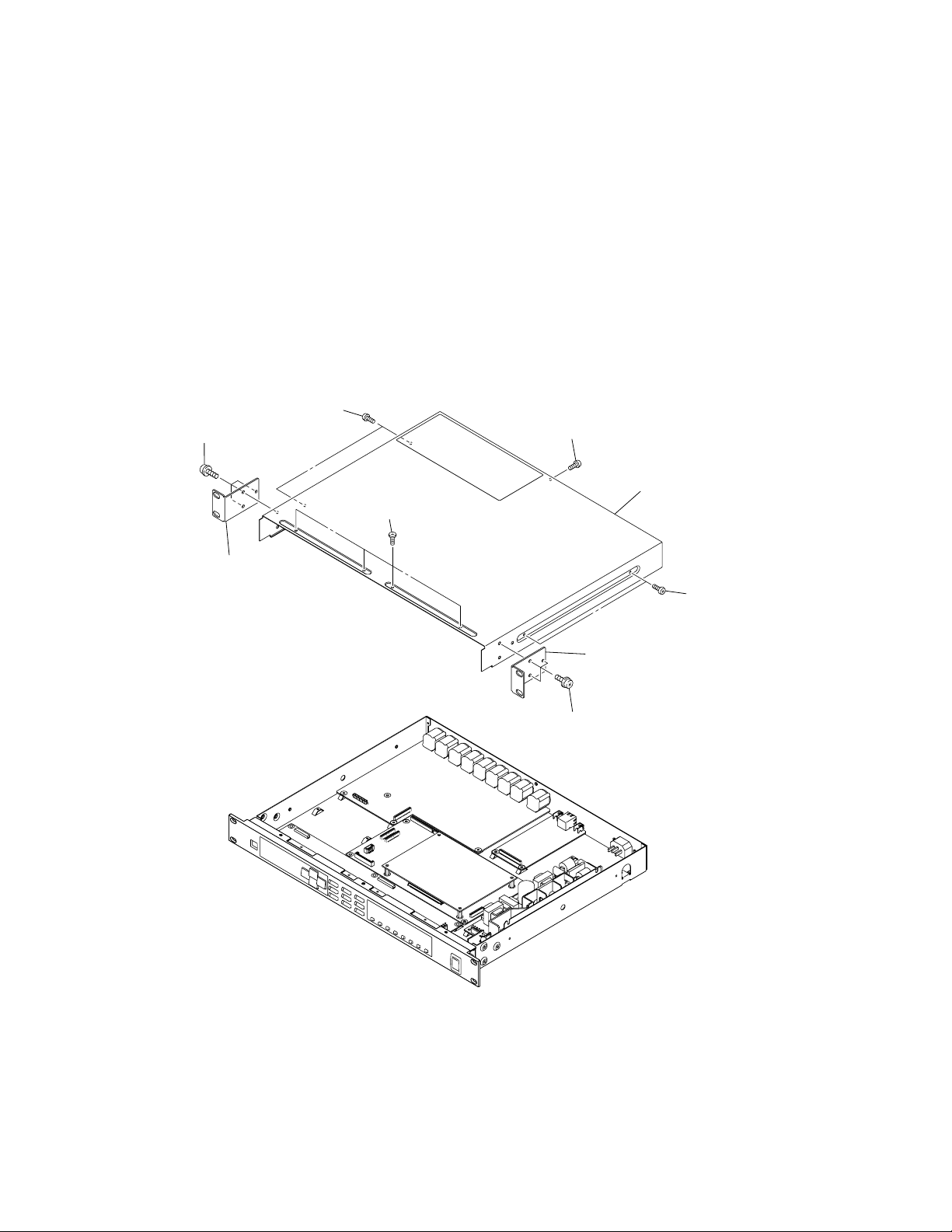
■ DISASSEMBLY PROCEDURES (分解手順)
1. Rack Angle (Time required: About 1 min.)
1-1. Remove the three (3) screws marked [1050]. The rack
angle L can then be removed. (Fig. 1)
1-2. Remove the three (3) screws marked [1020]. The rack
angle R can then be removed. (Fig. 1)
2. Top Cover (Time required : About 2 min.)
2-1. Remove the rack angle L and R. (See procedure 1)
2-2. Remove the five (5) screws marked [990] and four (4)
screws marked [980]. The top cover can then be removed.
[990]
[1050]
[980]
Rack angle L
(ラックアングルL)
1. ラックアングル(所要時間:約1分)
1-1. [1050]のネジ3本を外し、ラックアングルLを外しま
す。(図1)
1-2. [1020]のネジ3本を外し、ラックアングルRを外しま
す。(図1)
2. トップカバー(所要時間:約2分)
2-1. ラックアングルL、Rを外します。(1項参照)
2-2. [990 ]のネジ5本、[980]のネジ4本を外し、トップカ
バーを外します。(図1)
[990]
Top cover
(トップカバー)
[990]
Rack angle R
(ラックアングルR)
[1020]
[980]: Special Flat Head Screw-S 3x6 MFZN2B3 (WF054700) Sタイト
[990]: Bind Head Tapping Screw-S 3x6 MFZN2B3 (WE877800) Sタイト+BIND
[1020]: Bind Head Tapping Screw-B 4x8 MFZN2B3 (WE986200) Bタイト+BIND
[1050]: Bind Head Tapping Screw-B 4x8 MFZN2B3 (WE986200) Bタイト+BIND
10
(Fig. 1)
(図1)
SP2060
[940]
Front panel
(フロントパネル)
Bottom viewTop view
[950]
3. Front Panel (Time required: About 3 min.)
3-1. Remove the rack angle L and R. (See procedure 1)
3-2. Remove the top cover. (See procedure 2)
3-4. Remove the screw marked [940] and three (3) screws
marked [950].
The front panel can then be removed. (Fig. 2)
[940]: Special Flat Head Screw-S 3x6 MFZN2B3 (WF054700) Sタイト
[950]: Bind Head Tapping Screw-S 3x6 MFZN2B3 (WE877800) Sタイト+BIND
3. フロントパネル(所要時間:約3分)
3-1. ラックアングルL、Rを外します。(1項参照)
3-2. トップカバーを外します。(2項参照)
3-3. [940]のネジ1本と[950]のネジ3本を外し、フロントパ
ネルを外します。(図2)
(Fig. 2)
(図2)
11

SP2060
4. ANA Circuit Board (Time required: About 5 minutes.)
4-1. Remove the rack angle L and R. (See procedure 1)
4-2. Remove the top cover. (See procedure 2)
4-3. Remove the six (6) screws marked [240], twelve (12)
screws marked [250] and four (4) screws marked [260].
The ANA circuit board can then be removed. (Fig. 3, 4)
5. ENT Circuit Board (Time required : About 4 minutes.)
5-1. Remove the rack angle L and R. (See procedure 1)
5-2. Remove the top cover. (See procedure 2)
5-3. Remove the two (2) screws marked [500] and two (2)
screws marked [510]. The ENT circuit board can then
be removed. (Fig. 3, 4)
6. Power Supply Unit and Dividing Board (Time required : About 5 min.)
6-1. Remove the rack angle L and R. (See procedure 1)
6-2. Remove the top cover. (See procedure 2)
6-3. Remove the two (2) screws marked [760] and two (2)
screws marked [790].
The power supply unit and dividing board can then be
removed. (Fig. 4)
4. ANAシート(所要時間:約5分)
4-1. ラックアングルL、Rを外します。(1項参照)
4-2. トップカバーを外します。(2項参照)
4-3. [240]のネジ6本、[250]のネジ12本、[260]のネジ4本を
外し、ANAシートを外します。(図3、4)
5. ENTシート(所要時間:約4分)
5-1. ラックアングルL、Rを外します。(1項参照)
5-2. トップカバーを外します。(2項参照)
5-3. [500]のネジ2本、[510]のネジ2本を外し、ENTシート
を外します。(図3、4)
6. 電源ユニット、仕切り板R
(所要時間:約5分)
6-1. ラックアングルL、Rを外します。(1項参照)
6-2. トップカバーを外します。(2項参照)
6-3. [760]のネジ2本と[790]のネジ2本を外し、電源ユニッ
ト、および仕切り板Rを外します。(図4)
7. AC Inlet Assembly (Time required : About 3 min.)
7-1. Remove the rack angle L and R. (See procedure 1)
7-2. Remove the top cover. (See procedure 2)
7-3. Remove the two (2) screws marked [140] and screw
marked [150]. The AC inlet assembly can then be removed. (Fig. 3, 4)
8. DC Circuit Board (Time required : About 4 minutes.)
8-1. Remove the rack angle L and R. (See procedure 1)
8-2. Remove the top cover. (See procedure 2)
8-3. Remove the three (3) screws marked [100]. The DC cir-
cuit board can then be removed. (Fig. 4)
7. ACインレットAssy(所要時間:約3分)
7-1. ラックアングルL、Rを外します。(1項参照)
7-2. トップカバーを外します。(2項参照)
7-3. [140]のネジ2本、[150]のネジ1本を外し、ACインレッ
トAssyを外します。(図3、4)
8. DCシート(所要時間:約4分)
8-1. ラックアングルL、Rを外します。(1項参照)
8-2. トップカバーを外します。(2項参照)
8-3. [100]のネジ3本を外し、DCシートを外します。(図4)
12
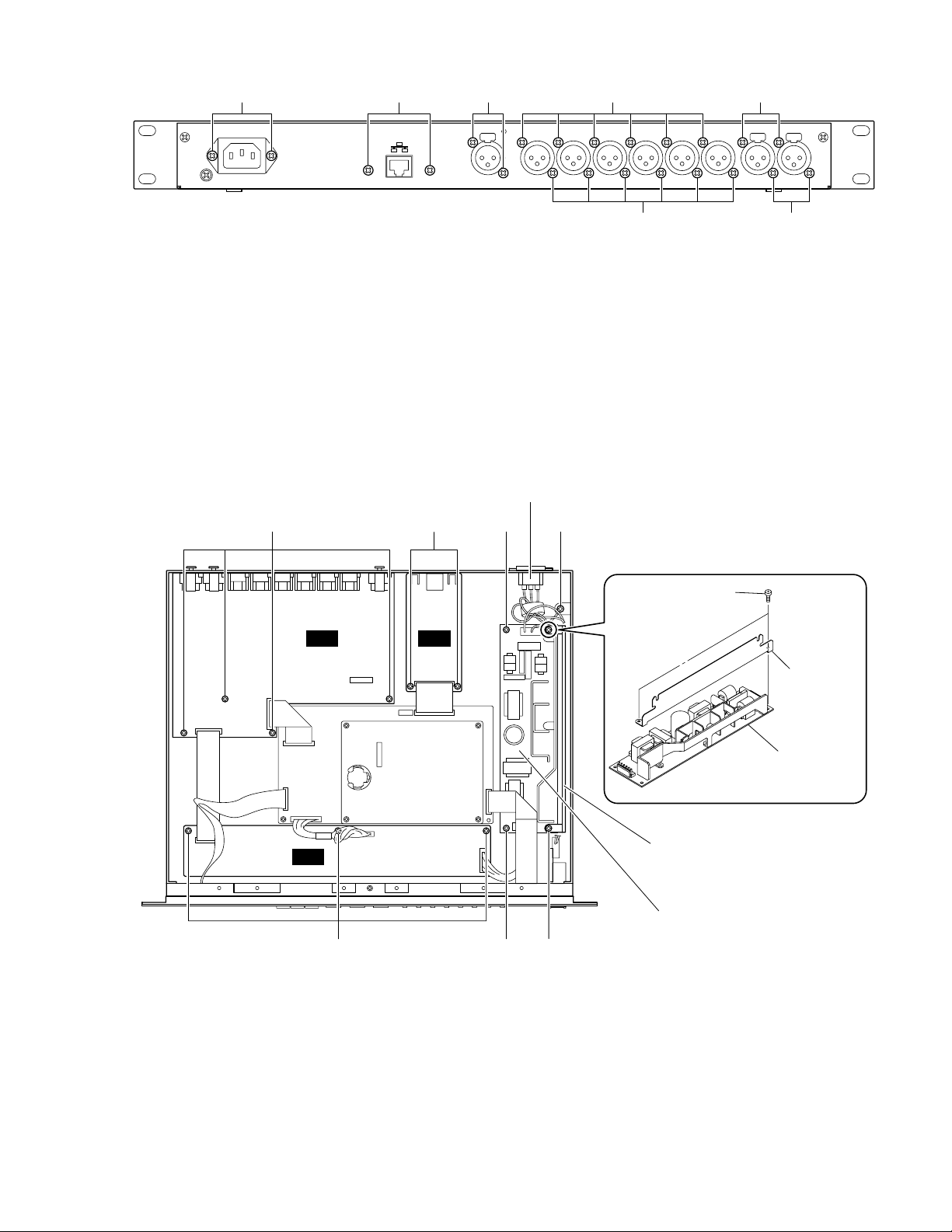
SP2060
[260]
[790]
[100]
AC inlet assembly
(ACインレットAss'y)
Power supply unit
(電源ユニット)
Power supply unit
(電源ユニット)
Dividing board
(仕切板R)
Dividing board
(仕切板R)
[760] [150]
[760] [790]
DC
ANA ENT
[510]
Rear view
[140] [500] [240][250]
[140]: Bind Head Tapping Screw-B 3x8 MFZN2B3 (WE774400) Bタイト+BIND
[240]: Bind Head Tapping Screw-B 3x8 MFZN2B3 (WE774400) Bタイト+BIND
[250]: Bind Head Tapping Screw-B 3x8 MFZN2B3 (WE774400) Bタイト+BIND
[500]: Bind Head Tapping Screw-S 3x6 MFZN2B3 (WE877800) Sタイト+BIND
[240]
[250] [240]
(Fig. 3)
(図3)
[100]: Bind Head Tapping Screw-S 3x6 MFZN2B3 (WE877800) Sタイト+BIND
[150]: Bind Head Tapping Screw-S 4x8 MFZN2B3 (WE994800) Sタイト+BIND
[260]: Bind Head Tapping Screw-S 3x6 MFZN2B3 (WE877800) Sタイト+BIND
[510]: Bind Head Tapping Screw-S 3x6 MFZN2B3 (WE877800) Sタイト+BIND
[760]: Bind Head Tapping Screw-S 3x6 MFZN2W3 (WH673900) Sタイト+BIND
[790]: Bind Head Tapping Screw-S 3x6 MFZN2W3 (WH673900) Sタイト+BIND
(Fig. 4)
(図4)
13

SP2060
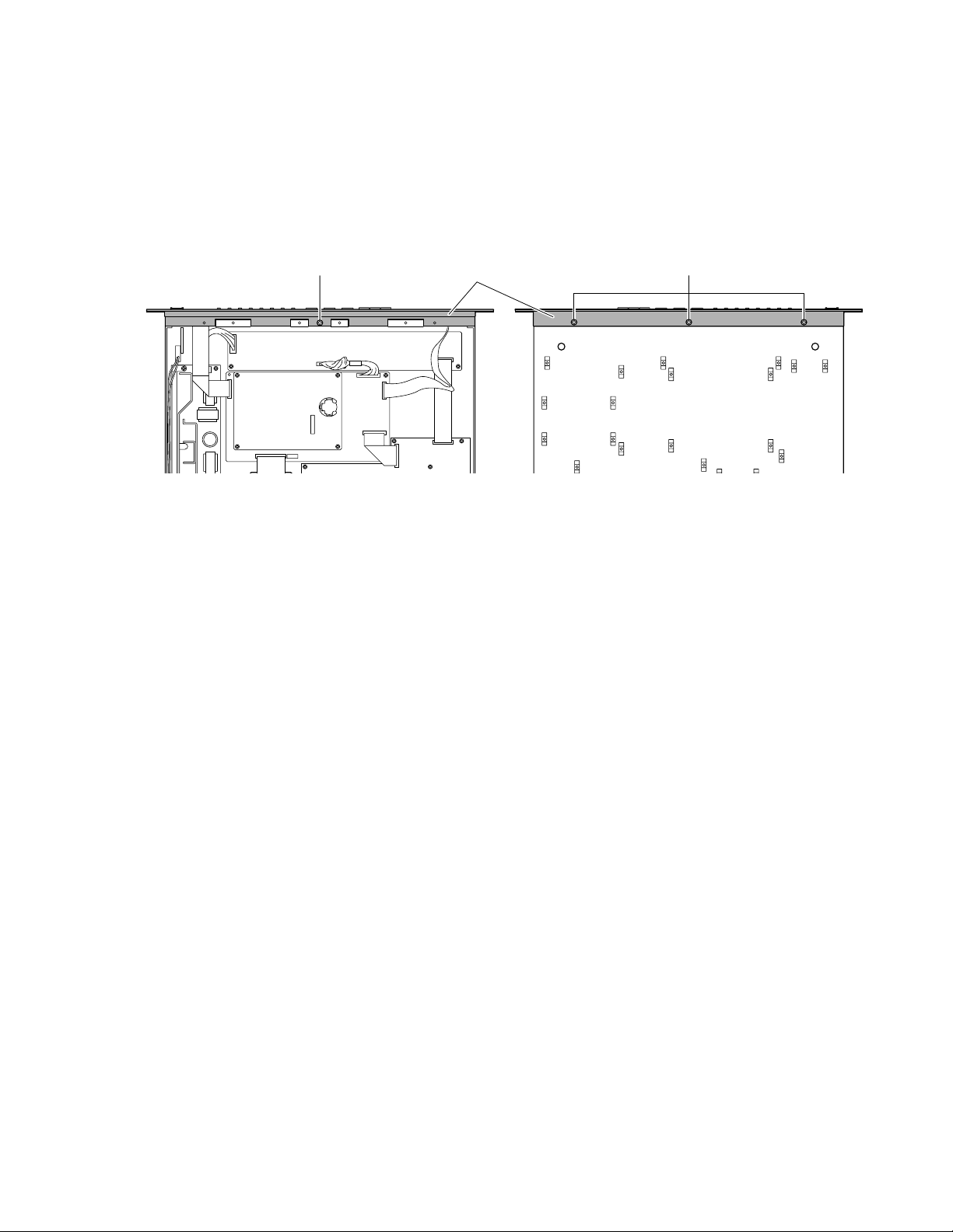
9. CPU Circuit Board (Time required : About 4 minutes.)
9-1. Remove the rack angle L and R. (See procedure 1)
9-2. Remove the top cover. (See procedure 2)
9-3. Remove the four (4) screws marked [70]. The CPU cir-
cuit board can then be removed. (Fig. 5)
10. Replacing the Lithium Battery (Time required : About 3 min.)
10-1. Remove the rack angle L and R. (See procedure 1)
10-2. Remove the top cover. (See procedure 2)
10-3. You can replace the lithium battery from the CPU circuit
board. (Fig. 5)
* The lithium battery is not part of the CPU circuit board.
When you replace the CPU circuit board, you should
remove the lithium battery from the CPU board on
the main unit, and install it in the holder on the new
CPU circuit board.
* Save the important data to an external device (such
as a computer) with the backup function of the DME
Designer (version 2.0 or later) in advance.
For more information on the operation, refer to the
DME Designer owner’s manual.
9. CPUシート(所要時間:約4分)
9-1. ラックアングルL、Rを外します。(1項参照)
9-2. トップカバーを外します。(2項参照)
9-3. [70]のネジ4本を外し、CPUシートを外します。(図5)
10. リチウム電池の交換(所要時間:約3分)
10-1. ラックアングルL、Rを外します。(1項参照)
10-2. トップカバーを外します。(2項参照)
10-3. CPUシート上よりリチウム電池を交換することができ
ます。(図5)
* リチウム電池は、CPUシートの構成部品ではありま
せん。
CPUシートを交換する際には、本体のCPUシートか
らリチウム電池を取り外して、新しいCPUシートに
取り付けてください。
* 重要なデータは、あらかじめDMEDesigner(バー
ジョン2.0以上)のバックアップ機能でパソコンなど
の外部機器に保存してください。
その操作方法の詳細は、DMEDesigner取扱説明書
を参照してください。
11. DSP Circuit Board (Time required : About 5 minutes.)
11-1. Remove the rack angle L and R. (See procedure 1)
11-2. Remove the top cover. (See procedure 2)
11-3. Remove the CPU Circuit Board. (See procedure 9)
11-4. Remove the two (2) screws marked [30] and four (4)
hexagonal spacers marked [40].
The DSP circuit board can then be removed. (Fig. 5)
11. DSPシート(所要時間:約5分)
11-1. ラックアングルL、Rを外します。(1項参照)
11-2. トップカバーを外します。(2項参照)
11-3. CPUシートを外します。(9項参照)
11-4. [30]のネジ2本、[40]の六角スペーサー4本を外し、
DSPシートを外します。(図5)
14
SP2060
● Lithium Battery(リチウム電池)
CPUDSP
Battery VN103500
VN103600(Battery holder for VN103500)
Notice for back-up battery removal
Push the battery as shown in figure,
then the battery will pop up.
Druk de batterij naar beneden zoals
aangeven in de tekening, de batterij
springt dan naar voren.
Battery
Battery holder
[40]
[40]
DSP
[70][30]
[70][30]
[30]: Bind Head Tapping Screw-S 3x6 MFZN2B3 (WE877800) Sタイト+BIND
[40]: Hexagonal Spacer L=13 (WG501800) 六角スペーサーM3
[70]: Bind Head Tapping Screw-S 3x6 MFZN2B3 (WE877800) Sタイト+BIND
(Fig. 5)
(図5)
15
SP2060
12. LCD Module
(Time required : About 4 minutes.)
12-1. Remove the rack angle L and R. (See procedure 1)
12-2. Remove the top cover. (See procedure 2)
12-3. Remove the front panel. (See procedure 3)
12-4. Remove the two (2) screws marked [640]. The LCD
module can then be removed. (Fig. 6)
13. Meter Assembly
(Time required : About 4 minutes.)
13-1. Remove the rack angle L and R. (See procedure 1)
13-2. Remove the top cover. (See procedure 2)
13-3. Remove the front panel. (See procedure 3)
13-4. Remove the screw marked [570]. The meter assembly
can then be removed. (Fig. 6)
14. PS Circuit Board (Time required : About 4 minutes.)
14-1. Remove the rack angle L and R. (See procedure 1)
14-2. Remove the top cover. (See procedure 2)
14-3. Remove the front panel. (See procedure 3)
14-4. Remove the button PSW. (Fig. 6)
14-5. Remove the two (2) screws marked [190]. The PS cir-
cuit board can then be removed. (Fig. 6)
12. 液晶ディスプレイ(所要時間:約4分)
12-1. ラックアングルL、Rを外します。(1項参照)
12-2. トップカバーを外します。(2項参照)
12-3. フロントパネルを外します。(3項参照)
12-4. [6 4 0 ]のネジ2本を外し、液晶ディスプレイを外しま
す。(図6)
13. メーターAssy(所要時間:約4分)
13-1. ラックアングルL、Rを外します。(1項参照)
13-2. トップカバーを外します。(2項参照)
13-3. フロントパネルを外します。(3項参照)
13-4. [570]のネジを外し、メーターAssyを外します。(図6)
14. PSシート(所要時間:約4分)
14-1. ラックアングルL、Rを外します。(1項参照)
14-2. トップカバーを外します。(2項参照)
14-3. フロントパネルを外します。(3項参照)
14-4. ボタンPSWを外します。(図6)
14-5. [190]のネジ2本を外し、PSシートを外します。(図6)
LCD Module
(液晶ディスプレイ)
[640] [190]
[190]: Bind Head Tapping Screw-S 3x6 MFZN2B3 (WE877800) Sタイト+BIND
[570]: Bind Head Tapping Screw-S 3x6 MFZN2B3 (WE877800) Sタイト+BIND
[640]: Bind Head Tapping Screw-B 2.6x8 MFZN2B3 (WE961700) Bタイト+BIND
Meter Assembly
(メーターAss'y)
(Fig. 6)
(図6)
[570] [190]
PS
Button PSW
(ボタンPSW)
16
SP2060
■ LSI PIN DESCRIPTION (LSI端子機能表)
CONTENTS (目次)
• AK4393-VF-E2 (XW029A00) DAC (Digital to Analog Converter) ......... 17
• AK5385BVF-E2 (X5364B00) ADC (Analog to Digital Converter) ......... 17
• HD6417727F160CV (X2890B00) CPU (Microprocessor 32 bit) ............ 18
• YSS919B-HZ (XZ693B00) DSP7 (Digital Signal Processor)................. 20
• KSZ872ISL (X5621A00) PHYceiver ........................................................ 22
• LC4032V-75TN48C (X7109A00)
CPLD (Complex Programmable Logic Device) ..................................22
• AK4393-VF-E2 (XW029A00) DAC (Digital to Analog Converter) ANA: IC101, 201, 301
Pin
Name I/O Function
no.
1
10
11
12
13
14
DVSS
2
DVDD
3
MCLK
4
PD
5
BICK
6
SDATA
7
LRCK
8
SMUTE
CS
9
DFS
DEM0
CCLK
DEM1
CDTI
DIF0
DIF1
DIF2
-
Digital Ground Pin
-
Digital Power Supply Pin, 3.3V or 5.0V
I
Master Clock Input Pin
I
Power-Down Mode Pin
When at “L”,the Ak4393 is in power-down mode and
is held in reset.
The AK4393 should always be reset upon powerup.
I
Audio Serial Data Clock Pin
The clock of 64fs or more than is recommended to
be input on this pin.
I
Audio Serial Data Input Pin
2’s complement MSB-first data is input on this pin.
I
L/R Clock Pin
I
Soft Mute Pin
When this pin goes “H”, soft mute cycle is initiated.
When returning “L”,the output mute releases.
I
Chip Select Pin in serial mode
I
Doubla speed sampling mode Pin (Internal pull-down
pin)
“L”: Normal Speed, “H”: Double Speed
I
De-emphasis Enable pin
I
Control Data Clock Pin in serial mode
I
De-emphasis Enable pin
I
Control Data Input Pin in serial mode
I
I
Digital Input Format Pin
I
Pin
Name I/O Function
no.
15
16
17
18
19
20
21
22
23
24
25
26
27
28
BVSS
VREFL
VREFH
AVD D
AVSS
AOUTR-
AOUTR+
AOUTL-
AOUTL+
VCOM
P/S
CKS0
CKS1
CKS2
I
Substrate Ground Pin, 0V
I
Low Level Voltage Reference Input Pin
-
High Level Voltage Reference Input Pin
-
Analog Power Supply Pin, 5V
O
Analog Ground Pin, 0V
O
Rch Negative analog output Pin
O
Rch Positive analog output Pin
O
Lch Negative analog output Pin
O
Lch Positive analog output Pin
O
Common Voltage Output Pin, 2.6V
Parallel/Serial Select Pin (Internal pull-up pin)
I
“L”: Serial control mode, “H”: Parallel control mode
I
I
Master Clock Select Pin
I
• AK5385BVF-E2 (X5364B00) ADC (Analog to Digital Converter) ANA: IC501
Pin
Name I/O Function
no.
1
10
11
12
13
14
VREFL
2
AVSS
3
VCOM
4
LIN+
5
LIN-
6
CKS0
7
DVDD
8
DVSS
9
OVF
PDN
DIF
M/S
LRCK
BICK
I
Lch voltage reference input
-
Analog ground
O
Common voltage output
I
Lch analog positive input
I
Lch analog negative input
I
Master clock select 0
-
Digital power supply
-
Digital ground
O
Analog input overflow detect
I
Power down mode
I
Audio interface format
I
Master / Slave mode
I/O
Output channel clock
I/O
Audio serial data clock
Pin
Name I/O Function
no.
15
16
17
18
19
20
21
22
23
24
25
26
27
28
SDTO
CKS1
MCLK
DFS0
HPFE
DFS1
BVSS
AVSS
AVD D
RIN-
RIN+
TEST
AVSS
VREFR
Audio serial date output
O
Master clock select
I
Master clock input
I
I
Sampling speed select 0
High pass filter enable
I
Sampling speed select 1
I
Substrate ground
Analog ground
Analog power supply
-
I
Rch analog negative input
Rch analog positive input
I
Test pin
I
Analog ground
Rch voltage reference input
I
17
SP2060
• HD6417727F160CV (X2890B00) CPU (Microprocessor 32 bit) CPU: IC002
Pin
no.
1
2
3
4
5
6
7
8
IRQ0/IRL0_/PTH[0]
9
IRQ1/IRL1_/PTH[1]
10
IRQ2/IRL2_/PTH[2]
11
IRQ3/IRL3_/PTH[3]
12
13
14
15
16
17
18
19
20
21
22
23
24
25
26
27
28
29
30
31
32
33
34
35
36
37
38
39
40
41
42
43
44
45
46
47
48
49
50
51
52
53
54
55
56
57
58
59
60
61
62
63
64
65
IRQ4/PTH[4]
D31/PTB[7]
D30/PTB[6]
D29/PTB[5]
D28/PTB[4]
D27/PTB[3]
D26/PTB[2]
D25/PTB[1]
D24/PTB[0]
D23/PTA[7]
D22/PTA[6]
D21/PTA[5]
D20/PTA[4]
D19/PTA[3]
D18/PTA[2]
D17/PTA[1]
D16/PTA[0]
Name I/O Function
Vcc-RTC
XTAL2
EXTAL2
Vss-RTC
MD1
MD2
NMI
VEPWC
VCPWC
MD5
/BREQ
/BACK
VssQ
CKIO2
VccQ
VssQ
VccQ
Vss
Vcc
D15
VssQ
D14
VccQ
D13
D12
D11
D10
D9
D8
D7
D6
VssQ
D5
VccQ
D4
D3
D2
D1
D0
A0
A1
A2
VssQ
A3
-
Power supply for RTC (1.9V)
-
Not in use (XTAL for internal RTC)
-
-
Power supply for RTC (0V)
-
Clock mode setting
-
-
Not in use (Non-maskable interrupt request)
I
I
I
External interrupt request
I
I
O
VEE control pin for LCD panel
-
VCC control pin for LCD panel
-
Big endian setting
-
Not in use (bus request)
-
Bus acknowledge
-
VssQ
-
System clock output
-
VccQ
I/O
I/O
I/O
I/O
Data bus
I/O
I/O
I/O
I/O
-
VssQ
I/O
Data bus
-
VccQ
I/O
I/O
Data bus
I/O
-
Vss
I/O
Data bus
-
Vcc
I/O
I/O
Data bus
I/O
-
-
VssQ
-
Data bus
-
VccQ
-
-
-
-
Data bus
-
-
-
-
-
VssQ
-
Data bus
-
VccQ
-
-
-
Data bus
-
-
-
-
Address bus
-
-
VssQ
-
Address bus
Pin
no.
66
67
68
69
70
71
72
73
74
75
76
77
78
79
80
81
82
83
84
85
86
87
88
89
90
91
92
93
94
95
96
97
98
99
100
101
102
103
104
105
106
107
108
109
110
111
112
113
114
115
116
117
118
119
120
121
122
123
124
125
126
127
128
129
130
Name I/O Function
VccQ
A4
A5
A6
A7
A8
A9
A10
A11
VssQ
A12
VccQ
A13
A14
A15
A16
A17
A18
A19
A20
VssQ
A21
VccQ
A22
A23
Vss
A24
Vcc
A25
BS_/PTK[4]
RD_
WE0_/DQMLL
WE1_/DQMLU/WE
WE2_/DQMUL/ICIORD_/PTK[6]
VssQ
WE3_/DQMUU/ICIOWR_/PTK{7}
VccQ
RD/WR_
PTE[7]/PCC0RDY/AUDSYNC_
/CS0
/CS2
/CS3
/CS4/PTK[2]
/CS5/CE1A_/PTK[3}
/CS6/CE1B_
CE2A_/PTE[4]
CE2B_/PTE[5]
AFE_HC1/USB1d_DPLS/PTK[0]
AFE_RLYCNT_/USB1d_DMNS/PTK[1]
VssQ
AFE_SCLK/USB1d_TXDPLS
VccQ
PTM[7]/PTINT[7]/AFE_FS/USB1d_RCV
PTM[6]/PTINT[6]/AFE_RXIN/USB1d_SPEED
PTM[5]/PTINT[5]/AFE_TXOUT/USB1d_TXSE0
PTM[4]/PINT[4]/AFE_RDET_/USB1d_TXDMNS
Reserved/USB1d_SUSPEND
USB1_ovr_crnt/USBF_VBUS
USB2_ovr_crnt_
RTS2_/USB1d_TXENL
PTE[2]/USB1_pwr_en
PTE[1]/USB2_pwr_en
CKE/PTK[5]
/RAS3/PTJ[0]
Reserved/PTJ[1]
-
VccQ
-
-
-
Address bus
-
-
-
-
-
VssQ
-
Address bus
-
VccQ
-
-
-
Address bus
-
-
-
-
-
VssQ
-
Address bus
-
VccQ
Address bus
-
-
Vss
-
Address bus
-
Vcc
-
Address bus
O
Not connected (bus cycle start signal)
-
Read strobe
O
Write 0 signal
O
Write 1 signal
O
Write 2 signal
-
VssQ
O
Write 3 signal
-
VccQ
O
Read/Write
O
I/O
-
Chip Select 0
-
Chip Select 2
-
Chip Select 3
O
Chip Select 4
O
Chip Select 5
O
Chip Select 6
O
Output port (SWP50 Reset)
O
Output port (PLG Board Reset)
O
SPD DATA
O
SPD CL
-
VssQ
I
Not in use (USB1 D+ transmission)
-
VccQ
I
I
I
Not in use
I
O
I
USB function VBUS
-
USB2_HOST2 over current detection
O
Not in use
O
USB1 voltage control
O
USB2 voltage control
O
Enable (SDRAM)
O
RAS for SDRAM
O
Not in use
18
Pin
no.
131
132
133
134
135
136
137
138
139
140
141
142
143
144
145
146
147
148
149
150
151
152
153
154
155
156
157
158
159
160
161
162
163
164
165
166
167
168
169
170
171
172
173
174
175
176
177
178
179
180
181
182
183
184
185
Name I/O Function
Reserved//CAS/PTJ[2]
VssQ
Reserved/PTJ[3]
VccQ
Reserved/PTJ[4]
Reserved/PTJ[5]
Vss
PTD[5]/CL1
Vcc
PTD[7]/DON
PTE[6]/M_DISP
PTE[3]/FLM
PTE[0]/TDO
PCC0RESET/DRACK0
PCC0DRV_/DACK0_
/WAIT
/RESETM
/ADTRG/PTH[5]
/IOIS16/PTG[7]
/ASEMD0
PTG[5]/ASEBRKAK_
PTG[4]
PCC0BVD2/PTG[3]/AUDATA[3]
PCC0BVD1/PTG[2]/AUDATA[2]
Vss
PCC0CD2/PTG[1]/AUDATA[1]
Vcc
PCC0CD1/PTG[0]/AUDATA[0]
VssQ
PTF[7]/PINT[15]/TRST_
VccQ
PTF[6]/PINT[14]/TMS
PTF[5]/PINT[13]/TDI
PTF[4]/PINT[12]/TCK
PTF[3]/PINT[11]/Reserved
PCCREG_/PTF[2]/Reserved
PCC0VS1_/PTF[1]/Reserved
PCC0VS2_/PTF[0]/Reserved
MD0
Vcc-PLL1
CAP1
Vss-PLL1
Vss-PLL2
CAP2
Vcc-PLL2
PCC0WAIT_/PTH[6]/AUDCK
Vss
Vcc
XTAL
EXTAL
LCD15/PTM[3]/PINT[10]
LCD14/PTM[2]/PINT[9]
LCD13/PTM[1]/PINT[8]
LCD12/PTM[0]
STATUS0/PTJ[6]
CAS for SDRAM
O
VssQ
Output port (DAC Reset)
O
VccQ
Output port (SIO Reset)
O
Output port (DAC Mute)
O
Vss
LCD line clock
O
Vcc
LCD DISPLAY ON
O
LCD alternater
O
LCD frame line marker
O
JTAG (test data output)
O
DMA request acceptance
O
DMA acknowledge
O
Hardware wait request
Manual reset request
Analog A/D trigger
I
I
-
Not in use
I
I
I
Vss
Not in use
I
Vcc
Not in use
I
VssQ
Not in use
I
VccQ
-
I
I
I
Not in use
I
I
I
I
Clock mode setting
Power supply for Vcc_PLL1 - PLL1(1.9V)
External capacitance for CAP1 _ PLL1
Power supply for Vss_PLL1 _ PLL1(0V)
Power supply for Vss_PLL2 _ PLL2 (0V)
External capacitance for CAP2 _ PLL2
Power supply for Vcc_PLL2 _ PLL2 (1.9V)
Not in use
I
Vss
Vcc
Clock oscillator
External clock
-
I
Not in use
I
I
Input port (Flash ROM RY/BY)
I
Output port (Flash ROM write protect)
O
Pin
no.
186
STATUS1/PTJ[7]
187
188
189
190
191
192
193
194
195
196
197
198
199
200
201
202
203
204
205
206
207
208
209
210
211
212
213
214
215
216
217
218
219
220
221
222
223
224
225
226
227
228
229
230
231
232
233
234
235
236
237
238
239
240
CL2/PTH[7]
TxD0/SCPT[0]
SCK0/SCPT[1]
TxD_SIO/SCPT[2]
SIOMCLK/SCPT[3]
TxD2/SCPT[4]
SCK_SIO/SCPT[5]
SIOFSYNC/SCPT[6]
RxD0/SCPT[0]
RxD_SIO/SCPT[2]
RxD2/SCPT[4]
SCPT[7]/CTS2_/IRQ5
LCD11/PTC[7]/PINT[3]
LCD10/PTC[6]/PINT[2]
LCD9/PTC[5]/PINT[1]
VssQ
LCD8/PTC[4]/PINT[0]
VccQ
LCD7/PTD[3]
LCD6/PTD[2]
LCD5/PTC[3]
LCD4/PTC[2]
LCD3/PTC[1]
LCD2/PTC[0]
LCD1/PTD[1]
LCD0/PTD[0]
DREQ0_/PTD[4]
LCK/UCLK/PTD[6]
/RESETP
CA
MD3
MD4
/Scan_testen
Avcc_USB
USB1_P
USB1_M
Avss_USB
USB2_P
USB2_M
Avcc_USB
Avss
AN[2]/PTL[2]
AN[3]/PTL[3]
AN[4]/PTL[4]
AN[5]/PTL[5]
Avcc
AN[6]/PTL[6]/DA[1]
AN[7]/PTL[7]/DA[0]
Avss
Name I/O Function
Output port (Flash ROM ACC)
O
LCD clock output
VssQ
CKIO
VccQ
Vss
Vcc
O
VssQ
System clock input/output (for SDRAM)
VccQ
Output port for SCI
O
O
Not in use
O
O
Output port for SCI
O
O
Not in use
O
Receiving data 0
I
Not in use
I
Vss
Receiving data 2
I
Vcc
Not in use
I
Output port (PLG CLOCK ON/OFF)
O
O
Not in use
O
VssQ
Not in use
O
VccQ
LCD DATA7
O
LCD DATA6
O
LCD DATA5
O
LCD DATA4
O
LCD DATA3
O
LCD DATA2
O
LCD DATA1
O
LCD DATA0
O
DMA request
I
USB clock
I
Power on reset request
Hardware standby request
Bus width setting for area0
-
Test pin (fixed to 3.3V)
USB analog power supply (3.3V)
USB1 data input/output (+)
I/O
USB1 data input/output (-)
I/O
USB analog power supply (0V)
USB2 data input/output (+)
I/O
USB2 data input/output (-)
I/O
USB analog power supply (3.3V)
A/D analog power supply (0V)
-
I
I
AD converter input
I
I
A/D analog power supply (3.3V)
AD converter input
I
DA converter output (LCD contrast)
O
A/D analog power supply (0V)
-
SP2060
CPU: IC002
19
SP2060
• YSS919B-HZ (XZ693B00) DSP7 (Digital Signal Processor) DSP: IC153
Pin
no.
10
11
12
13
14
15
16
17
18
19
20
21
22
23
24
25
26
27
28
29
30
31
32
33
34
35
36
37
38
39
40
41
42
43
44
45
46
47
48
49
50
51
52
Name I/O Function
1
2
3
4
5
6
7
8
9
PLLEN
/TEST
AVss
CPO
AVdd
Vss
Vdd
/IC
/MUTE
/SSYNC
MCKS
XI
BTYP
/CS
/WR
/RD
CA7
CA6
CA5
CA4
CA3
CA2
Vss
Vdd
CD31/CA1
CD30
CD29
CD28
CD27
CD26
CD25
CD24
Vdd
Vss
CD23
CD22
CD21
CD20
CD19
CD18
CD17
CD16
Vss
Vdd
CD15
CD14
CD13
CD12
CD11
CD10
CD09
CD08
I
PLL enable input (0: PLL unuse, 1: PLL use)
I
Test mode setting (0: TEST, 1: Normal)
Analog ground
PLL filter
Power supply (2.5 V)
Ground
Power supply (3.3 V)
I
Initial clear
I Mute control (0: SIO mute, 1: SIO nor mal in-out)
I
I
Serial I/O Sync. signal input
I
Serial I/O master clock input (128 x Fs)
I
System master clock input (60 MHz or 15 MHz)
I
Data bus type select (0: 16 bits, 1: 32 bits)
I
Chip select
I
Write enable input
I
Read enable input
I
I
I
CPU address bus
I
I
I
Ground
Power supply (3.3 V)
I/O
CPU data bus / CPU address bus
I/O
I/O
I/O
I/O
CPU data bus
I/O
I/O
I/O
Power supply (2.5 V)
Ground
I/O
I/O
I/O
I/O
CPU data bus
I/O
I/O
I/O
I/O
Ground
Power supply (3.3 V)
I/O
I/O
I/O
I/O
CPU data bus
I/O
I/O
I/O
I/O
Pin
no.
53
54
55
56
57
58
59
60
61
62
63
64
65
66
67
68
69
70
71
72
73
74
75
76
77
78
79
80
81
82
83
84
85
86
87
88
89
90
91
92
93
94
95
96
97
98
99
100
101
102
103
104
Name I/O Function
Vss
CD07
CD06
CD05
CD04
CD03
CD02
CD01
CD00
N.C.
Vdd
Vss
Vdd
SIO00
SIO01
SIO02
SIO03
SIO04
SIO05
SIO06
SIO07
Vss
SIO08
SIO09
SIO10
SIO11
SIO12
SIO13
SIO14
SIO15
Vss
Vdd
SIO16
SIO17
SIO18
SIO19
SIO20
SIO21
SIO22
SIO23
Vdd
Vss
SIO24
SIO25
SIO26
SIO27
SIO28
SIO29
SIO30
SIO31
Vss
Vdd
Ground
I/O
I/O
I/O
I/O
CPU data bus
I/O
I/O
I/O
I/O
No connect
Power supply (2.5 V)
Ground
Power supply (3.3 V)
I/O
I/O
I/O
I/O
Serial data bus
I/O
I/O
I/O
I/O
Ground
I/O
I/O
I/O
I/O
Serial data bus
I/O
I/O
I/O
I/O
Ground
Power supply (3.3 V)
I/O
I/O
I/O
I/O
Serial data bus
I/O
I/O
I/O
I/O
Power supply (2.5 V)
Ground
I/O
I/O
I/O
I/O
Serial data bus
I/O
I/O
I/O
I/O
Ground
Power supply (3.3 V)
20
Pin
no.
105
106
107
108
109
110
111
112
113
114
115
116
117
118
119
120
121
122
123
124
125
126
127
128
129
130
131
132
133
134
135
136
137
138
139
140
141
142
143
144
145
146
147
148
149
150
151
152
153
154
155
156
Name I/O Function
SIO32
SIO33
SIO34
SIO35
SIO36
SIO37
SIO38
SIO39
Vdd
Vss
SIO40
SIO41
SIO42
SIO43
SIO44
SIO45
SIO46
SIO47
Vss
Vdd
SIO48
SIO49
SIO50
SIO51
SIO52
SIO53
SIO54
SIO55
Vss
SIO56
SIO57
SIO58
SIO59
SIO60
SIO61
SIO62
SIO63
Vdd
Vss
Vdd
DA00
DA01
DA02
DA03
DA04
DA05
DA06
DA07
Vss
DA08
DA09
DA10
I/O
I/O
I/O
I/O
Serial data bus
I/O
I/O
I/O
I/O
Power supply (2.5 V)
Ground
I/O
I/O
I/O
I/O
Serial data bus
I/O
I/O
I/O
I/O
Ground
Power supply (3.3 V)
I/O
I/O
I/O
I/O
Serial data bus
I/O
I/O
I/O
I/O
Ground
I/O
I/O
I/O
I/O
Serial data bus
I/O
I/O
I/O
I/O
Power supply (2.5 V)
Ground
Power supply (3.3 V)
I/O
I/O
I/O
I/O
Memory data bus
I/O
I/O
I/O
I/O
Ground
I/O
Memory data bus
I/O
I/O
Pin
no.
157
158
159
160
161
162
163
164
165
166
167
168
169
170
171
172
173
174
175
176
177
178
179
180
181
182
183
184
185
186
187
188
189
190
191
192
193
194
195
196
197
198
199
200
201
202
203
204
205
206
207
208
Name I/O Function
DA11
DA12
DA13
DA14
DA15
Vss
Vdd
DA16
DA17
DA18
DA19
DA20
DA21
DA22
DA23
Vdd
Vss
DA24
DA25
DA26
DA27
DA28
DA29
DA30
DA31
Vss
Vdd
/WE
/CAS
SDCK
CKE
/RAS
Vdd
Vss
BA1
BA0
A12
A11
A10
A09
A08
Vss
Vdd
A07
A06
A05
A04
A03
A02
A01
A00
Vss
I/O
I/O
Memory data bus
I/O
I/O
I/O
Ground
Power supply (3.3 V)
I/O
I/O
I/O
I/O
Memory data bus
I/O
I/O
I/O
I/O
Power supply (2.5 V)
Ground
I/O
I/O
I/O
I/O
Memory data bus
I/O
I/O
I/O
I/O
Ground
Power supply (3.3 V)
Memory write enable signal
O
Column address strobe
O
Clock (SDRAM)
O
CKE (SDRAM)
O
Row address strobe
O
Power supply (2.5 V)
Ground
O
Bank select (SDRAM)
O
O
O
Memory address (SDRAM, DRAM)
O
O
O
Ground
Power supply (3.3 V)
O
O
O
O
Memory address (SDRAM, DRAM)
O
O
O
O
Ground
SP2060
DSP: IC153
21
SP2060
• KSZ872ISL (X5621A00) PHYceiver ENT: IC109
Pin
no.
1
2
3
4
5
6
7
8
9
10
11
12
13
14
15
16
17
18
19
20
21
22
23
24
Name I/O Function
MDIO
MDC
RXD3/PHYAD
RXD2/PHYAD2
RXD1/PHYAD3
RXD0/PHYAD4
VDDIO
GND
RXDV/CRSDV/PCS_LPBK
RXC
RXER/ISO
GND
VDDC
TXER
TXC/REFCLK
TXEN
TXD0
TXD1
TXD2
TXD3
COL/RMII
CRS/RMII_BTB
GND
VDDIO
I/O
Management Independent Interface (MII)
Data I/O.
I
MII Clock Input.
Ipd/O
Ipd/O
MII Receiver Data Output.
Ipd/O
Ipd/O
Pwr
Digital IO 2.5/3.3V tolerant power supply.
GND
Ground.
Ipd/O
MII Receiver Data Valid Output.
O
MII Receiver Clock Output. Operating at
25MHz=100Mbps, 2.5MHz=10Mbps.
Ipd/O
MII Receiver Error Output.
GND
Ground.
Pwr
Digital core 2.5V only power supply.
Ipd
MII Transmit Error Input.
I/O
MII Transmit Clock Output.
Ipd
MII Transmit Enable Input.
Ipd
Ipd
MII Transmit Data Input.
Ipd
Ipd
Ipd/O
MII Collision Detect Output.
Ipd/O
MII Carrier Sense Output.
GND
Ground.
Pwr
Digital IO 2.5/3.3V tolerant power supply.
Pin
no.
25
26
27
28
29
30
31
32
33
34
35
36
37
38
39
40
41
42
43
44
45
46
47
48
Name I/O Function
INT#/PHYAD0
LED0/TEST
LED1/SPD100/noFEF
LED2/
LED3/NWAYEN
PD#
VDDRX
RX-
RX+
FXSD/FXEN
GND
GND
REXT
VDDRCV
GND
TX-
TX+
VDDTX
GND
GND
XO
XI
VDDPLL
RST#
Ipd/O
Management Interface (MII) Interrupt Out.
Ipd/O
Link/Activity LED Output.
Ipd/O
Speed LED Output.
Ipd/O
Full-duplex LED Output.
Ipd/O
Collision LED Output.
Ipd
Power Down. 1=Normal operation, 0=Powerdown, Active low.
Pwr
Analog 2.5V power supply.
I
Receive Input: Differential receive input pins
for 100FX, 100BaseTX, or 10BaseT.
I
Ipd/O
Fiber Mode Enable/Signal Detect in Fiber
Mode.
GND
Ground.
GND
I
External resistor (6.49 kΩ) connects to
REXT and GND.
Pwr
Analog 2.5V power supply.
GND
Ground.
O
Transmit Outputs: Differential transmit output for 100FX, 100BaseTX, or 10BaseT.
O
Transmit Outputs: Differential transmit output for 100FX, 100BaseTX, or 10BaseT.
Pwr
Transmitter 2.5V power supply.
GND
Ground.
GND
O
XTAL feedback: Used with XI for Xtal application.
I
Crystal Oscillator Input: Input for a crystal
or an external 25 MHz clock.
Pwr
Analog PLL 2.5V power supply.
Ipu
Chip Reset. Active low, minimum of 50µs
pulse is required.
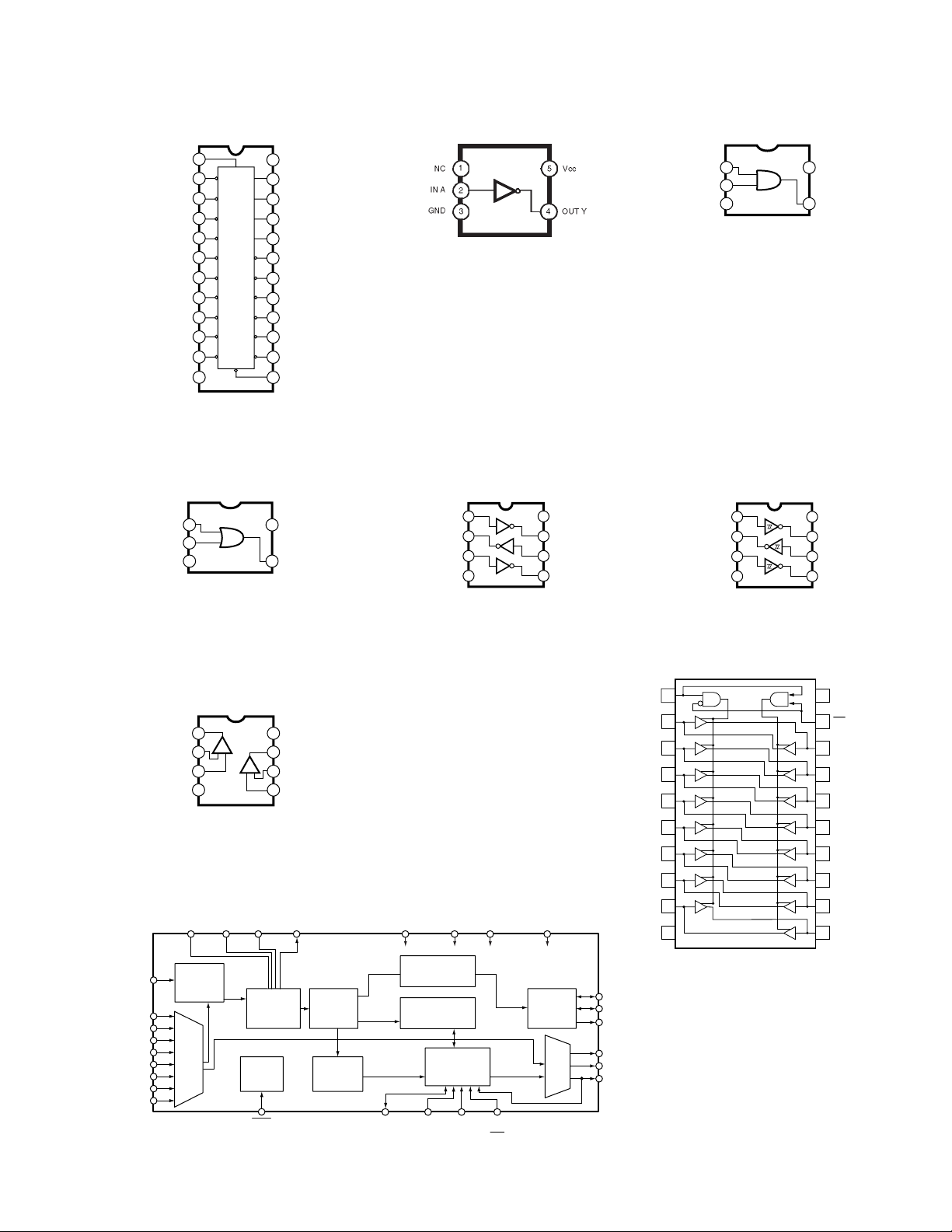
• LC4032V-75TN48C (X7109A00) CPLD (Complex Programmable Logic Device) CPU: IC014
PIN
No.
1
2
3
4
5
6
7
8
9
10
11
12
13
14
15
16
17
18
19
20
21
22
23
24
NAME
TDI
A5
A6
A7
GND0
VCCO0
A8
A9
A10
A11
TCK
VCC
GND
A12
A13
A14
A15
CLK1/I
CLK2/I
B0
B1
B2
B3
B4
I/O
I
Test data in
I/O
I/O
Input/Output
I/O
-
Ground
-
Power supply +3.3 V
I/O
I/O
Input/Output
I/O
I/O
I
Test clock input
-
Power supply +3.3 V
-
Ground
I/O
I/O
Input/Output
I/O
I/O
I/O
CLK input/Input
I/O
I/O
I/O
I/O
Input/Output
I/O
I/O
FUNCTION
PIN
NAME FUNCTION
No.
25
TMS
26
27
28
29
GND1
30
VCCO1
31
32
33
B10
34
B11
35
TDO
36
VCC
37
GND
38
B12
39
B13
40
B14
41
B15/GOE1
42
CLK3/I
43
CLK0/I
44
A0/GOE0
45
46
47
48
B5
B6
B7
B8
B9
A1
A2
A3
A4
I/O
I
Test mode select
I/O
I/O
Input/Output
I/O
-
Ground
-
Power supply +3.3 V
I/O
I/O
Input/Output
I/O
I/O
O
Test data out
-
Power supply +3.3 V
-
Ground
I/O
I/O
Input/Output
I/O
I/O
Input/Output / Global output enable input
I/O
CLK input/Input
I/O
I/O
Input/Output / Global output enable input
I/O
I/O
Input/Output
I/O
I/O
22
■ IC BLOCK DIAGRAM (ICブロック図)
SP2060
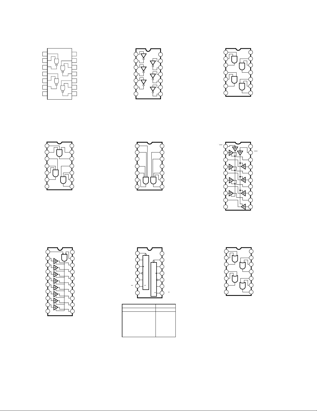
• 74VHC245MTCX_NF40 (X0296A00)
Bus Tranciever
CPU: IC003
V
CC
20
G
19
B1
18
B2
17
B3
16
B4
15
B5
14
B6
13
B7
12
B8
11
GND
1D1R
2
A1
A2
3
A3
4
A4
5
A5
6
A6
7
A7
8
A8
9
10
• NJM4556AL (XP844A00)
Operational Amplifier
ANA: IC105, 106, 205, 206, 305, 306
• NJM2068M-D (TE2) (X3505A00)
Operational Amplifier
ANA: IC401, 402
+-
+V
+DC Voltage
8
Supply
Output B
7
Inverting
6
Input B
Non-Inverting
5
Input B
Output A
Inverting
Input A
Non-Inverting
Input A
-DC Voltage Supply
1
2
+-
3
4
-V
• SN74AHC1G04DCKR (X4137A00)
Inverter
CPU: IC008
ENT: IC110
IN A
GND
1
NC
2
3
5
V
CC
4
OUT Y
• NJM2904V (TE1) (XR532A00)
Operational Amplifier
CPU: IC010
+DC Voltage
+-
+-
+V
8
Supply
Output B
7
Inverting
6
Input B
Non-Inverting
5
Input B
Output A
Inverting
Input A
Non-Inverting
Input A
Ground
1
2
3
4-V
• SN74AHC1G08DCKR AN (X3833A00)
Quad 2 Input AND
CPU: IC015
ENT: IC114
GND
1
A
2
B
3
5
Vcc
4
Y
• SN74AHC1G32DCKR (X4642A00)
Single 2 Input Positive OR Gate
ENT: IC111
Vcc5A1
B2
GND 3
Y4
• SN74AHCT08PWR (X3824A00)
Quad 2 Input AND
DSP: IC261
VSS
1
1A
2
1B
3
1Y
4
2A
5
2B
6
2Y
7
14
VDD
13
4B
12
4A
11
4Y
10
3B
9
3A
8
3Y
FUNCTION TABLE
INPUTS
AB Y
H
L
X
OUTPUT
H
X
L
H
L
L
• SN74AHCT245PWR (X2709A00)
Bus Tranceiver
DSP: IC016, 059, 250, 253, 258
1
D1R
GND
2
A1
3
A2
4
A3
5
A4
6
A5
7
A6
8
A7
A8
9
10
20
Vcc
19
G
18
B1
17
B2
16
B3
15
B4
14
B5
13
B6
12
B7
11
B8
23
SP2060
4B13
4A12
4Y11
3B10
3A9
3Y8
1B 2
1Y 3
2A 4
2B 5
2Y 6
GND 7
Vcc141A 1
• SN74LV00APWR (X4460A00)
Quad 2 Input Positive NAND Gate
DSP: IC050
• SN74LV11APWR (X3516A00)
Triple 3 Input AND
DSP: IC011
1
VSS
1A
1B
2
3
2A
4
2B
5
2C
6
2Y
7
14
VDD
1C
13
12
1Y
11
3C
10
3B
9
3A
8
3Y
• SN74LV04APWR (X5965A00)
Inverter
DSP: IC003, 018, 053, 257
Vss
1
1A
2
1Y
3
2A
4
2Y
5
3A
6
3Y
7
14
VDD
13
6A
12
6Y
11
5A
10
5Y
9
4A
8
4Y
• SN74LV21APWR (X2377A00)
Dual 4 Input AND
CPU: IC020
1
GND
1A
1B
2
3
NC
4
1C
5
1D
6
1Y
7
14
Vcc
2D
13
12
2C
11
NC
10
2B
9
2A
8
2Y
• SN74LV08APWR (X4463A00)
Quad 2 Input AND
DSP: IC051
1
VSS
1A
1B
2
1Y
3
4
2A
5
2B
6
2Y
7
14
VDD
4B
13
4A
12
11
4Y
10
3B
9
3A
8
3Y
• SN74LV244APWR (X3292A00)
Octal 3-State Bus Buffer
ANA: IC701, 703
DSP: IC152, 300, 450, 451
1A1
2Y4
1A2
2Y3
1A3
2Y2
1A4
2Y1
(GND) Vss
1 20
1G
2 19
3 18
4 17
5 16
6 15
7 14
8 13
9 12
10 11
VDD (Vcc)
2G
1Y1
2A4
1Y2
2A3
1Y3
2A2
1Y4
2A1
• SN74LV541APWRBUS B (X5966A00)
Octal 3-State Buffer
DSP: IC015
1
G1
2
A1
A2
3
4
A3
5
A4
6
A5
A6
7
A7
8
A8
9
10
GND
24
• SN74LV74APWR (X5534A00)
Dual D-Type Flip-Flop
DSP: IC056
20
Vcc
19
G2
18
Y1
17
Y2
16
Y3
15
Y4
Y5
14
13
Y6
12
Y7
11
Y8
1
1CLR
2
D
1D
3
1CK
1PR
GND
PR CLR CLK D Q Q
L
H
L
H
H
H
CK
4
PR
5
Q
1Q
6
Q
1Q
7
INPUTS OUTPUTS
X
H
X
L
X
L
f
H
f
H
L
H
14
VCC
13
CLR
X
X
X
H
L
X
2CLR
D
12
CLR
2D
11
CK
2CK
10
2PR
PR
9
Q
2Q
8
Q
2Q
H
L
H
H
L
O
Q
L
H
H
L
H
O
Q
• SN74LVC32APWR OR (X5405A00)
Quad 2 Input OR
ENT: IC115
1
GND
1A
1B
2
1Y
3
4
2A
5
2B
6
2Y
7
14
Vcc
4B
13
4A
12
11
4Y
10
3B
9
3A
8
3Y
SP2060
• SN74LVCC4245APWR (X3096A00)
Dual Supply Octal Bus Transceiver
DSP: IC251
1
VCCA
DIR
GND
GND
2
1
3
A1
2
4
A2
3
A3
5
4
6
A4
5
A5
7
6
8
7
A6
9
A7
8
10
9
A8
11
10 12
12
24
0
11
VCCB
23
VCCB
A
/G
22
B
B1
21
D
20
D
B2
19
G2
B3
18
G1
B4
15
17
B5
16
14
B6
15
13
B7
14
B8
13
GND
• TC7SH32FU (XW633A00)
Input OR Gate
ENT: IC111
IN B
1 5
2
IN A
3
GND
Vcc
4
OUT Y
• TC7SH04FU (XS775A00)
Inverter
ENT: IC110
• TC7WH04FU (XY363A00)
Triple Inverter
ANA: IC704
1
2
3Y
2A
3
GND
4
• TC7SH08FU (XR680A00)
2 Input AND Gate
ENT: IC114
IN B
1 5
2
IN A
3
GND
Vcc
4
OUT Y
• TC7WH14FU (XY806A00)
Schmitt Inverter
CPU: IC032
81A
Vcc
7
1Y
6
3A
5
2Y
GND
1
2
3Y
3
2A
4
81A
Vcc
7
1Y
6
3A
5
2Y
• uPC4570G2-E1-A (X7351A00)
Dual Operational Amplifier
ANA: IC103, 104, 203, 204, 303,
304, 403, 404
8
+-
V+
B OUTPUT
7
B
B -INPUT
6
B +INPUT
5
A OUTPUT
A -INPUT
A +INPUT
1
A
-+
2
3
4
V-
• CS8416-CZZR (X7363A00)
Digital Audio Interface Receiver
ANA: IC601
RXN
RXP0
RXP1
RXP2
RXP3
RXP4
RXP5
RXP6
RXP7
VA AGND FILT
Receiver
TX Passthrough
8:2
MUX
RMCK
Clock &
Data
Recovery
Misc.
Control
RST
AES3
S/PDIF
Decoder
Format
Detect
• SN74LV245APWR (X3693A00, XZ287A00)
Octal 3-State Bus Transceiver
ANA: IC702 (X3693A00)
CPU: IC021-026 (XZ287A00)
DSP: IC005-010 (X3693A00)
IC012-014 (X3693A00)
IC017 (X3693A00)
IC061-064 (X3693A00)
ENT: IC101-104 (X3693A00)
VD
VL DGND OMCK
De-emphasis
Filter
C & U bit
Data Buffer
Control
Port &
Registers
AD1/SCL/SDA/
Serial
Audio
Output
n:3
MUX
AD0/
DIR
A1
A2
A3
A4
A5
A6
A7
A8
GND
OLRCK
OSCLK
SDOUT
GPO0
GPO1
AD2/GPO2
1
2
3
4
5
6
7
8
9
10
20
Vcc
19
OE
18
B1
17
B2
16
B3
15
B4
14
B5
13
B6
12
B7
11
B8
25
SP2060
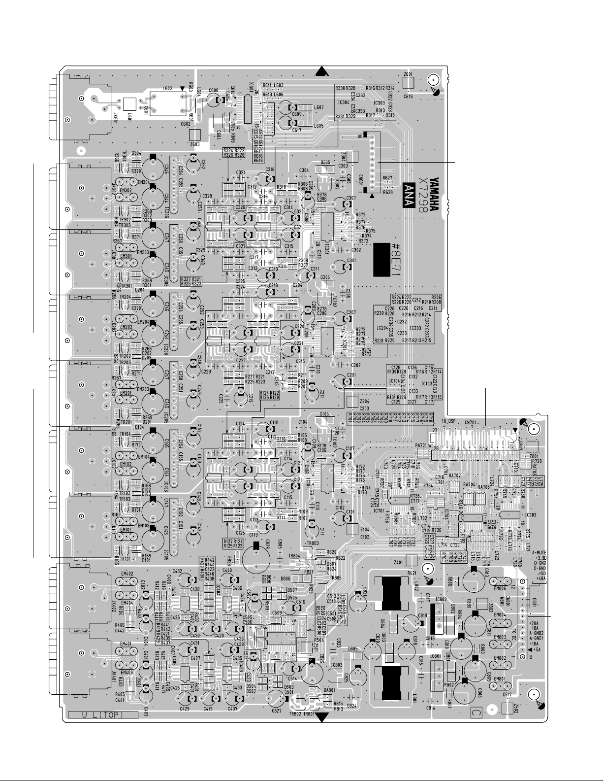
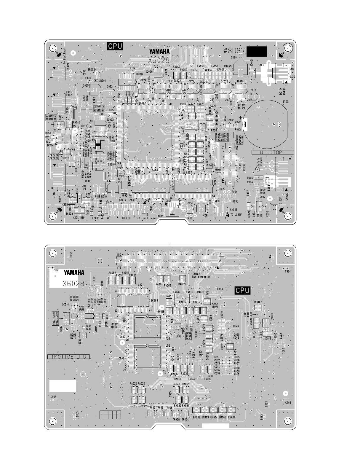
■ CIRCUIT BOARDS (シート基板図)
CONTENTS (目次)
• PS Circuit Board (X7297C0) ................................................26
• PN Circuit Board (X7297C0) ................................................27
• ANA Circuit Board (X7298C0) ................................................ 28
• CPU Circuit Board (X6028C0) ................................................30
• ENT Circuit Board (X7295C0) ................................................31
• DSP Circuit Board (X7296C0) ................................................ 32
• DC Circuit Board (X7297C0) ................................................34
Note: See parts list for details of circuit board component parts.
注:シートの部品詳細はパーツリストをご参照ください。
• PS Circuit Board
to AC INLET
to POWER SUPPLLY UNIT
Component side (部品側)
2NA-WG30340
POWER ON/OFF
Pattern side (パターン側)
2NA-WG30340
26
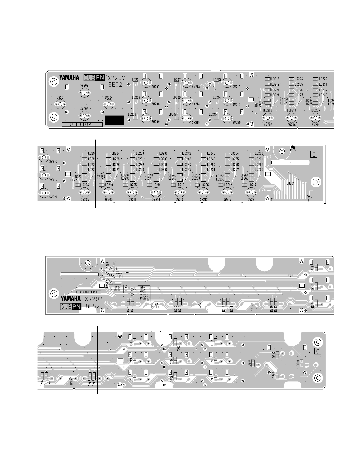
• PN Circuit Board
INC
BACK
NEXT
LEVEL
DELAY
SP2060
A'
EQ
DEC
ROUTING
SCENE
X-OVER
UTILITY
LIMITER
MUTE
A'
OVER
-6
-12
-18
-30
-48
B123456
A'
A
A'
OVER
LIMIT
-6
-12
-18
-40
to DSP- CN250
Component side (部品側)
B'
2NA-WG30340
B'
B'
B'
Pattern side (パターン側)
27
SP2060
• ANA Circuit Board
AES/EBU
Not used
OUTPUT
12 34 56
to DSP- CN450
to DC- CN103
INPUT A INPUT B DIGITAL INPUT
Component side (部品側)
28
2NA-WG30400
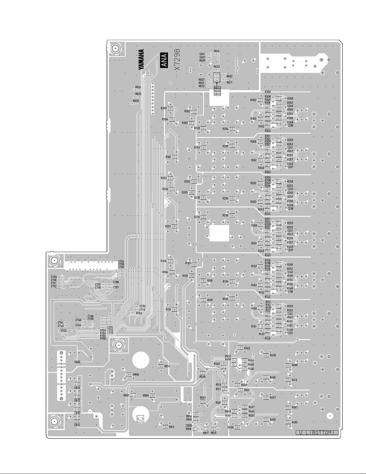
• ANA Circuit Board
SP2060
2NA-WG30400
Pattern side (パターン側)
29
SP2060
• CPU Circuit Board
to DSP- CN001
Component side (部品側)
30
Pattern side (パターン側)
2NA-WG30150
 Loading...