

Page 1
AV RECEIVER
RX-V579/TSR-5790
SERVICE MANUAL
Note:
When the DIGITAL P.C.B. or IC22 on DIGITAL P.C.B. is replaced, this unit will display “Internal Error” and will not
operate properly. The model name MUST be written to the backup IC (EEPROM: IC22 on DIGITAL P.C.B.) to have
proper operation. (For details, refer to “S5. SOFT SWITCH” menu of the self-diagnostic function.)
注意:
DIGITAL P.C.B. または DIGITAL P.C.B. の IC22 を交換すると、“Internal Error” が表示されて本機が正常に
なります
む必要があります。(詳細は、ダイアグの “S5. SOFT SWITCH” メニューを参照してください。)
。正常に動作させるために、モデル名をバックアップ IC(EEPROM:DIGITAL P.C.B. の IC22)へ書き込
動作しなく
■ CONTENTS
TO SERVICE PERSONNEL ........................................... 2
FRONT PANELS ............................................................ 3
REAR PANELS .......................................................... 4–7
REMOTE CONTROL PANEL ......................................... 8
SPECIFICATIONS / 参考仕様 .................................. 9–15
INTERNAL VIEW .........................................
S
ERVICE PRECAUTIONS / サービス時の注意事項 .... 16
DISASSEMBLY PROCEDURES / 分解手順 .......... 17–21
UPDATING FIRMWARE /
ファームウェアのアップデート ........................... 22–25
SELF-DIAGNOSTIC FUNCTION /
ダイアグ(自己診断機能) .................................... 26–62
POWER AMPLIFIER ADJUSTMENT /
パワーアンプ調整 ...................................................... 63
101337
................ 16
DISPLAY DATA ........................................
IC DATA .................................................................. 66–81
PIN CONNECTION DIAGRAMS ............................ 82–83
BLOCK DIAGRAMS ............................................... 84–85
WIRING DIAGRAMS .............................................. 86–87
PRINTED CIRCUIT BOARDS .............................. 88–102
SCHEMATIC DIAGRAMS .................................
REPLACEMENT PARTS LIST ............................115–137
REMOTE CONTROL .......................................... 138–139
CONFIGURING THE SYSTEM SETTINGS ................ 140
システム設定を変更する ............................................ 141
FIRMWARE UPDATING PROCEDURE ............. 142–147
ファームウェア更新手順 .................................... 148–153
.............. 6
..10
4–65
3–114
RX-V579/TSR-5790
IP
'15.10
Page 2
RX-V579/TSR-5790
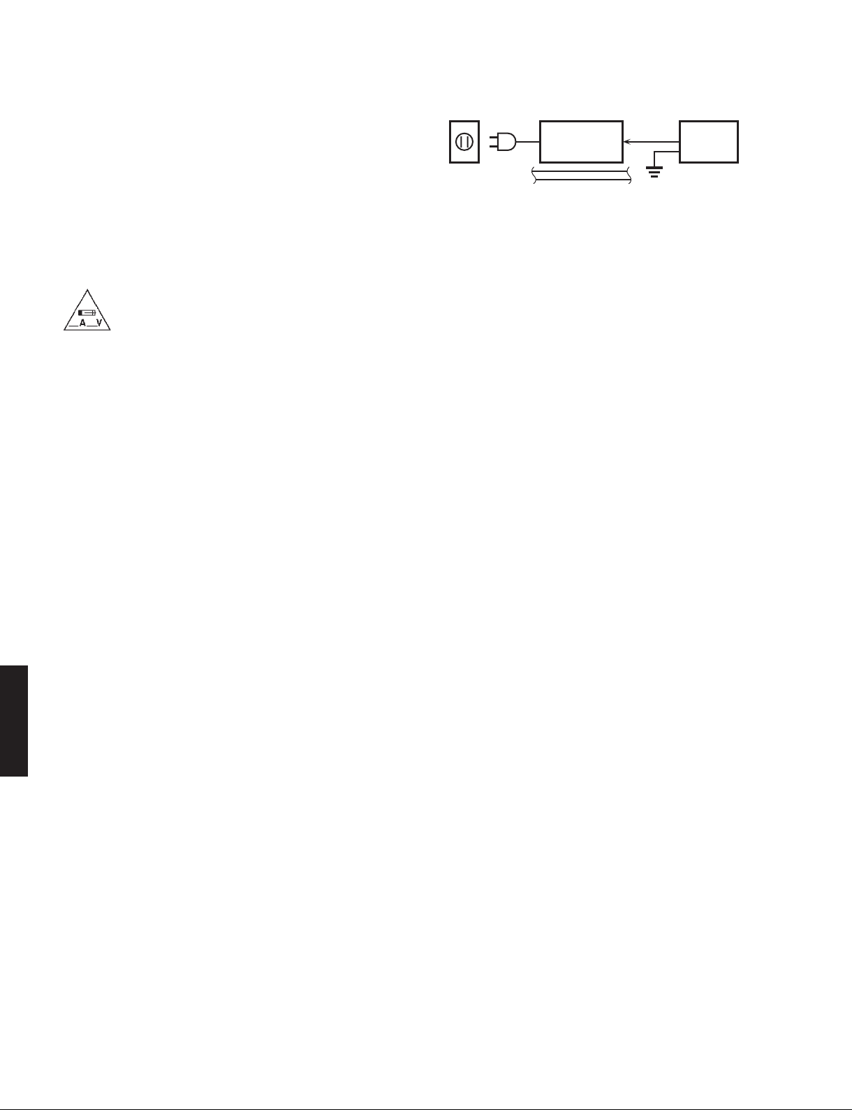
AC LEAKAGE
■ TO SERVICE PERSONNEL
1. Critical Components Information
Components having special characteristics are marked ⚠ and
must be replaced with parts having specifications equal to
those originally installed.
2. Leakage Current Measurement (For 120V Models Only)
When service has been completed, it is imperative to verify
that all exposed conductive surfaces are properly insulated
from supply circuits.
• Meterimpedanceshouldbeequivalentto1500ohmsshunted
by 0.15 μF.
For U model
“CAUTION”
“F5401: FOR CONTINUED PROTECTION AGAINST RISK OF FIRE, REPLACE ONLY WITH SAME TYPE 2A,
250V FUSE.”
“F5402: FOR CONTINUED PROTECTION AGAINST RISK OF FIRE, REPLACE ONLY WITH SAME TYPE 6A,
125V FUSE.”
For C model
CAUTION
F5401: REPLACE WITH SAME TYPE 2A, 250V FUSE.
F5402: REPLACE WITH SAME TYPE 6A, 125V FUSE.
ATTENTION
F5401: UTILISER UN FUSIBLE DE RECHANGE DE MÉME TYPE DE 2A, 250V.
F5402: UTILISER UN FUSIBLE DE RECHANGE DE MÉME TYPE DE 6A, 125V.
WALL
OUTLET
• Leakagecurrentmustnotexceed0.5mA.
• BesuretotestforleakagewiththeACpluginbothpolarities.
EQUIPMENT
UNDER TEST
INSULATING
TABLE
TESTER OR
EQUIVALENT
CALIFORNIA PROPOSITION 65 WARNING
This product contains chemicals known to the State of California to cause cancer, or birth defects or other reproductive
harm.
DO NOT PLACE SOLDER, ELECTRICAL/ELECTRONIC OR PLASTIC COMPONENTS IN YOUR MOUTH FOR ANY REASON
WHATSOEVER!
Avoid prolonged, unprotected contact between solder and your skin! When soldering, do not inhale solder fumes or
exp
ose eyes to solder/flux vapor!
If you come in contact with solder or components located inside the enclosure of this product, wash your hands before
handling food.
RX-V579/TSR-5790
About lead free solder / 無鉛ハンダについて
All of the P.C.B.s installed in this unit and solder joints are
soldered using the lead free solder.
Among some types of lead free solder currently available,
it is recommended to use one of the following types for
the repair work.
• Sn + Ag + Cu (tin + silver + copper)
• Sn + Cu (tin + copper)
• Sn + Zn + Bi (tin + zinc + bismuth)
Caution:
As the melting point temperature of the lead free solder is
about 30°C to 40°C (50°F to 70°F) higher than that of
the lead solder, be sure to use a soldering iron suitable to
each solder.
本機に搭載されているすべての基板およびハンダ付けに
よる接合部は無鉛ハンダでハンダ付けされています。
無鉛ハンダにはいくつかの種類がありますが、修理時に
は下記のような無鉛ハンダの使用を推奨します。
• Sn+Ag+Cu(錫 + 銀 + 銅)
• Sn+Cu(錫 + 銅)
• Sn+Zn+Bi(錫 + 亜鉛 + ビスマス)
注意:
無鉛ハンダの融点温度は通常の鉛入りハンダに比べ 30 〜
40℃程度高くなっていますので、それぞれのハンダに合っ
たハンダごてをご使用ください。
2
Page 3
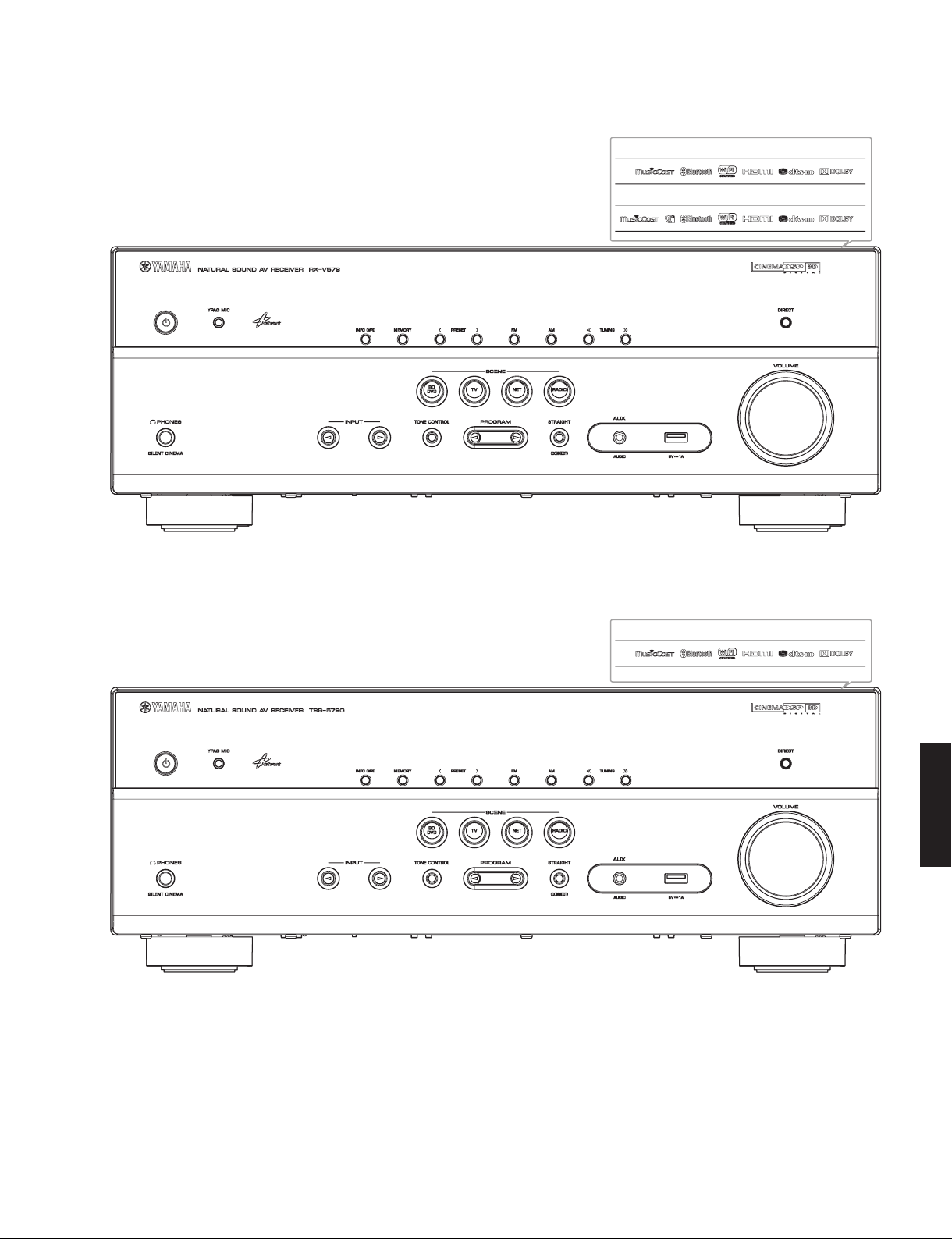
■ FRONT PANELS
RX-V579
RX-V579/TSR-5790
U, C, R, T, K, A, B, G, F, L, V, H models
J model
TSR-5790
RX-V579/TSR-5790
3
Page 4
RX-V579/TSR-5790
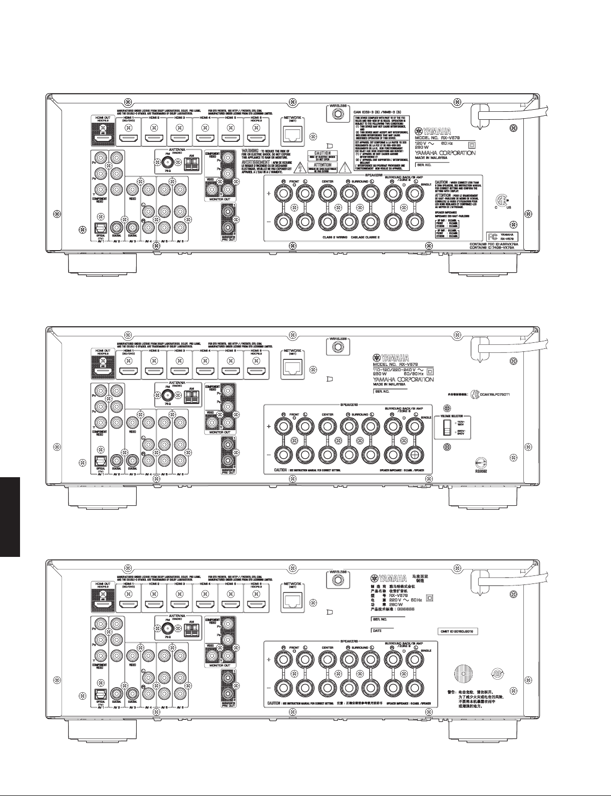
■ REAR PANELS
RX-V579 (U, C models)
RX-V579 (R, V models)
RX-V579/TSR-5790
RX-V579 (T model)
4
Page 5
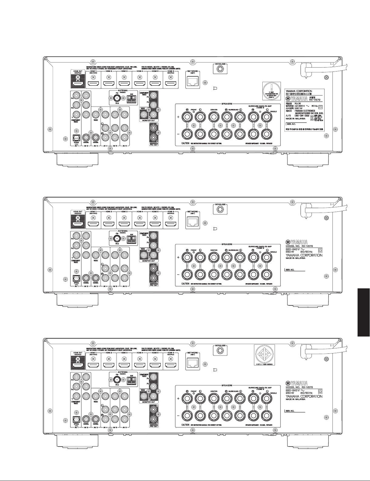
RX-V579 (K model)
RX-V579 (L model)
RX-V579/TSR-5790
RX-V579 (H model)
RX-V579/TSR-5790
5
Page 6
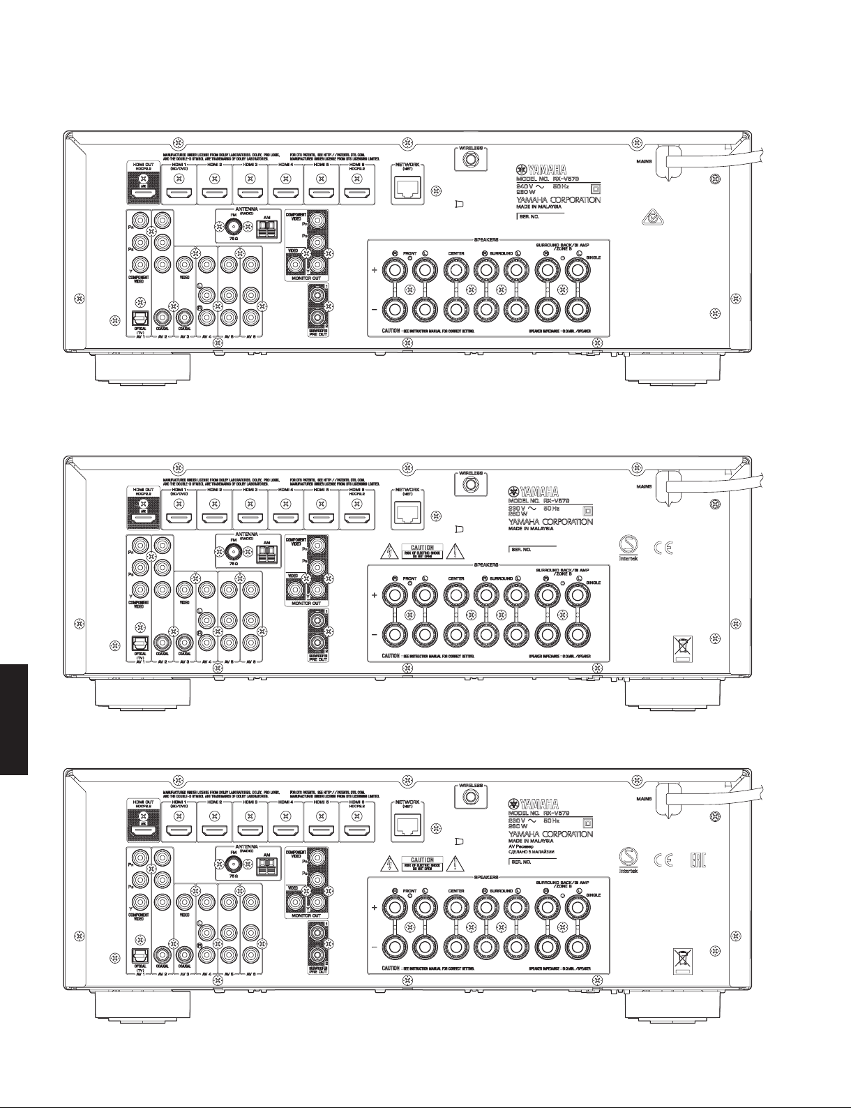
RX-V579/TSR-5790
RX-V579 (A model)
RX-V579 (B model)
RX-V579 (G, F models)
RX-V579/TSR-5790
6
Page 7
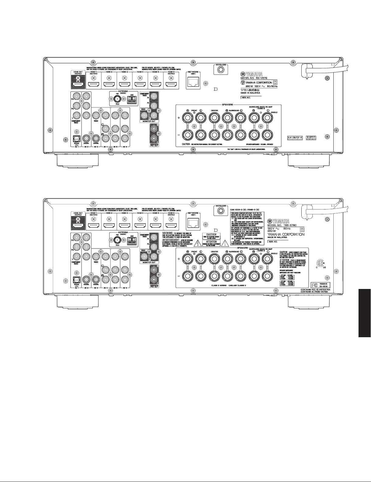
RX-V579 (J model)
TSR-5790 (U model)
RX-V579/TSR-5790
RX-V579/TSR-5790
7
Page 8
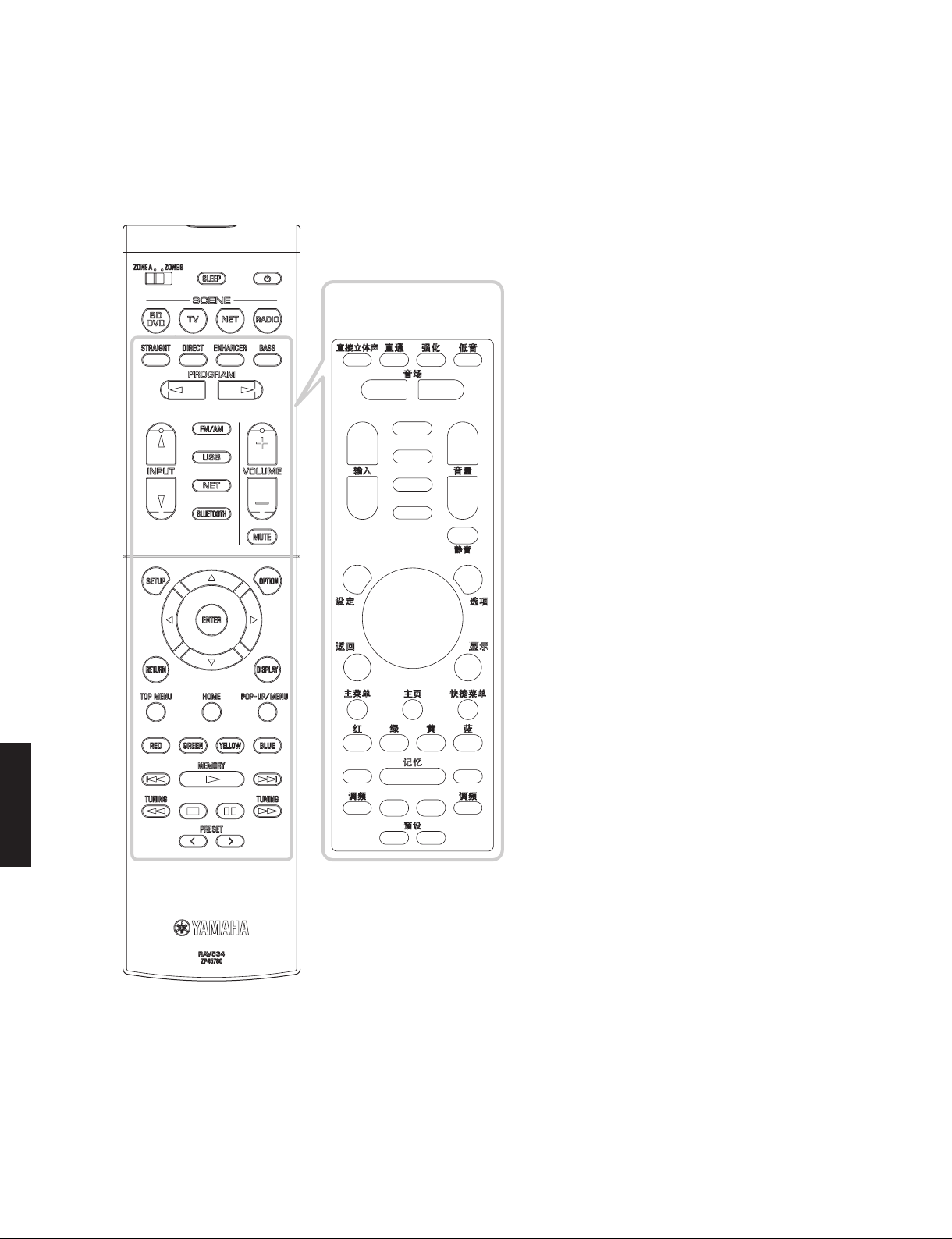
RX-V579/TSR-5790
RAV534
■ REMOTE CONTROL PANEL
Remote control sheet
(T model)
RX-V579/TSR-5790
8
Page 9

■ SPECIFICATIONS / 参考仕様
■ Audio Section / オーディオ部
RX-V579/TSR-5790
Rated Output Power (Power Amp. Section) /
定格出力(パワーアンプ部)
(1 kHz, 0.9 % THD)
– 1 channel driven –
U, C models (8 ohms)
FRONT L/R ..................................................................115 W/ch
CENTER .......................................................................115 W/ch
SURROUND L/R ..........................................................115 W/ch
SURROUND BACK L/R ...............................................115 W/ch
R, T, K, A, B, G, F, L, V, H, J models (6 ohms)
FRONT L/R ..................................................................115 W/ch
CENTER .......................................................................115 W/ch
SURROUND L/R ..........................................................115 W/ch
SURROUND BACK L/R ...............................................115 W/ch
– 2 channels driven simultaneously –
U, C models (8 ohms)
FRONT L/R ............................................................ 95 W + 95 W
CENTER ..............................................................................95 W
SURROUND L/R .................................................... 95 W + 95 W
SURROUND BACK L/R ......................................... 95 W + 95 W
(20 Hz to 20 kHz, 0.09 % THD)
– 2 channels driven simultaneously –
U, C models (8 ohms)
FRONT L/R ............................................................ 80 W + 80 W
R, T, K, A, B, G, F, L, V, H, J models (6 ohms)
FRONT L/R ............................................................ 80 W + 80 W
Maximum Effective Output Power / 実用最大出力
(1 kHz, 10 % THD, 1 channel driven)
R, T, K, A, B, G, F, L, V, H, J models (6 ohms)
FRONT L/R ...........................................................................135 W/ch
CENTER ...............................................................................135 W/ch
SURROUND L/R ..................................................................135 W/ch
SURROUND BACK L/R .......................................................135 W/ch
U, C models (8 ohms)
FRONT L/R ...........................................................................140 W/ch
CENTER ...............................................................................140 W/ch
SURROUND L/R ..................................................................140 W/ch
SURROUND BACK L/R .......................................................135 W/ch
Dynamic Power Per Channel / ダイナミックパワー
FRONT L/R (1 channel driven)
U, C models
(8 / 6 / 4 / 2 ohms) ....................................120 / 140 / 170 / 190 W
R, T, K, A, B, G, F, L, V, H, J models
(6 / 4 / 2 ohms) ..................................................120 / 140 / 170 W
Damping Factor / ダンピングファクタ
FRONT L/R to SPEAKER-A ..............................................100 or more
Input Sensitivity/Input Impedance / 入力感度/入力インピーダンス
(1 kHz, 100 W/8 ohms)
AV4 etc. ..............................................................200 mV / 47 k-ohms
Maximum Input Signal / 最大許容入力
AV4 etc. (EFFECT ON) ................................................................2.3 V
Output Level/Out
SUBWOOFER (2 ch stereo and FRONT SP: small)
............................................................................... 1 V / 1.2 k-ohms
put Impedance / 出力電圧/出力インピーダンス
(20 Hz to 20 kHz, 8 ohms)
(1 kHz, 0.5 % THD)
(JEITA)
(IHF)
Headphone Jack Rated Output/Output Impedance /
ヘッドホン出力/出力インピーダンス
AV4 etc. input.......................................................100 mV / 470 ohms
Frequency Response / 再生周波数帯域
AV4 etc., FRONT ................................................................... 0 / -3 dB
Signal to Noise Ratio / 信号対雑音比
AV4 etc. (DIRECT) to SP OUT (Input 1 k-ohm shorted)
................................................................................ 110 dB or more
Residual Noise / 残留ノイズ
FRONT L/R to SP OUT ................................................. 150 μV or less
Channel Separation / チャンネルセパレーション
AV4 etc. (Input 1 k-ohm shorted)
1 kHz / 10 kHz ................................. 70 dB or more / 50 dB or more
Volume Control/Step / 音量可変範囲/ステップ
........................................... MUTE / -80 dB to +16.5 dB / 0.5 dB step
Tone Control Characteristics / トーンコントロール特性
Bass
Boost/Cut ........................................ ±6 dB / 0.5 dB step, at 50 Hz
Turnover frequency ............................................................350 Hz
Treble
Boost/Cut ...................................... ±6 dB / 0.5 dB step, at 20 kHz
Turnover frequency ...........................................................3.5 kHz
Filter Characteristics / フィルタ特性
FRONT, CENTER, SURROUND, SURROUND BACK small (H.P.F.)
......................fc=40/60/80/90/100/110/120/160/200 Hz, 12 dB/oct.
SUBWOOFER small (L.P.F.)
......................fc=40/60/80/90/100/110/120/160/200 Hz, 24 dB/oct.
Optical Jack, Coaxial Jack Support Frequencies /
Optical 端子、Coaxial 端子 対応 fs
.................................................................................32 kHz to 96 kHz
■ Video Section / ビデオ部
Video Signal Type / ビデオ信号方式
U, C, R, K, V, J models...............................................................NTSC
T, A, B, G, F, L, H models ..............................................................PAL
Composite Video Signal Level / コンポジットビデオ信号
................................................................................ 1 Vp-p / 75 ohms
Component Video Signal Level / コンポーネントビデオ信号
Y .............................................................................. 1 Vp-p / 75 ohms
Pb/Pr .................................................................... 0.7 Vp-p / 75 ohms
Video Maximum Input Level / ビデオ最大許容入力
(VIDEO Conversion Off)
................................................................................. 1.5 Vp-p or more
Video Signal to Noise Ratio / ビデオ信号対雑音比
..................................................................................... 50 dB or more
Monitor Out Frequency Response / モニター出力周波数帯域
(VIDEO Conversion Off)
Component video signal level / コンポーネントビデオ信号
........................................................................ 5 Hz to 60 MHz, -3 dB
(IHF-A network)
(1 kHz, 50 mV, 8 ohms)
(10 Hz to 100 kHz)
(IHF-A network)
RX-V579/TSR-5790
9
Page 10

RX-V579/TSR-5790
■ FM Tuner Section / FM チューナー部
Tuning Range / 受信周波数範囲
U, C models .................................................. 87.5 MHz to 107.9 MHz
R, L
, V
, H models .......
T, K, A, B, G, F models ............................. 87.50 MHz to 108.00 MHz
J model ........................................................... 76.0 MHz to 94.9 MHz
50 dB Quieting Sensitivity /50 dB SN 感度
(1 kHz, 100 % MOD.)
Mono ...........................................................................3 μV (20.8 dBf)
Signal to Noise Ratio / 信号対雑音比
Mono ......................................................................................... 65 dB
Stereo ....................................................................................... 64 dB
Harmonic Distortion / 歪率
Mono ..........................................................................................0.5 %
Stereo ........................................................................................0.6 %
Antenna Input / アンテナ入力
.......................................................................... 75 ohms unbalanced
■ AM Tuner Section / AM チューナー部
Tuning Range / 受信周波数範囲
U, C models .............................................................530 to 1,710 kHz
R, L, V, H models .......................530 to 1,710 kHz / 531 to 1,611 kHz
T, K, A, B, G, F, J models .........................................531 to 1,611 kHz
Antenna / アンテナ
......................................................................................Loop antenna
■ General / 総合
Power Supply / 電源電圧
U, C models .............................................................. AC 120 V, 60 Hz
R, V models .................................. AC 110–120/220–240 V, 50/60 Hz
T model ..................................................................... AC 220 V, 50 Hz
K model ....................................................................AC 220 V, 60 Hz
A model ....................................................................AC 240 V, 50 Hz
B, G, F models .......................................................... AC 230 V, 50 Hz
L, H models ................................................. AC 220–240 V, 50/60 Hz
J model ................................................................ AC 100 V, 50/60 Hz
Power Consumption / 消費電力
RX-V579/TSR-5790
..................................................................................................260 W
Standby Power Consumption (reference data)
待機時消費電力(参考値)
Standby Through Off
(Selecting only when HDMI Control is Off) .............................0.1 W
Standby Through Auto (*1)
(INPUT: HDMI 1 (HDMI no signal)) .........................................0.4 W
Standby Through On
(INPUT: HDMI no signal) .........................................................1.6 W
Network Standby On (Wired)
Standby through Off ................................................................1.9 W
Standby through On ................................................................3.1 W
Network Standby On (Wireless)
Standby through Off ................................................................1.9 W
Standby through On ..................................................................2.8 W
Network Standby On (Wireless Direct)
Standby through Off ................................................................2.0 W
Standby through On ................................................................3.1 W
87.5 MHz to 108.0 MHz / 87.50 MHz to 108.00 MHz
(IHF)
(IHF)
(1 kHz)
/
Bluetooth Standby On
Standby through Off ................................................................2.0 W
Standby through On ................................................................3.1 W
(*1)
When HDMI no signal condition continues for 20 min., this product
makes the transition to "Stand by Through Off."
Maximum Power Consumption
..................................................................................................600 W
Dimensions (W x H x D) / 寸法(幅× 高さ× 奥行き)
.................................435 x 161 x 327 mm (17-1/8" x 6-3/8" x 12-7/8")
Reference Dimension with attaching wireless antenna (W x H x D)
/ 参照寸法(アンテナ直立時)(幅× 高さ× 奥行き)
................................435 x
Weight / 質量
.................................................................................8.1 kg (17.9 lbs.)
Finish / 仕上げ
[RX-V579]
T model ........................................................................... Gold color
U, C, R, T, K, A, B, G, F, L, V, H, J models .....................Black color
B, G, F, L models ....................................................... Titanium color
[TSR-5790]
U model..........................................................................Black color
Accessories / 付属品
Remote control............................................................................... x 1
Battery (R03, AAA, UM-4) .............................................................. x 2
FM antenna (1.4 m) ....................................................................... x 1
AM antenna (1 m) .......................................................................... x 1
YPAO microphone (6 m) ................................................................ x 1
Remote control sheet (T model) .................................................... x 1
Antenna isolator (T model) ............................................................ x 1
* Specifications are subject to change without notice.
※ 参考仕様および外観は、製品の改良のため予告なく変更すること
があります。
U ........................U.S.A. model
C ................. Canadian model
R .................... General model
T.....................Chinese model
K ......................Korean model
A .................Australian model
B .......................British model
[R, V models]
x 327 mm (17-1/8" x 8-3/4" x 12-7/8")
221
G ................. European model
F..................... Russian model
L................. Singapore model
V ...................... Taiwan model
H ...........................Thai model
J ...................Japanese model
10
Page 11
RX-V579/TSR-5790
Manufactured under license from Dolby Laboratories. Dolby, Pro
Logic, Surround EX, and the double-D symbol are trademarks of
Dolby Laboratories.
ドルビーラボラトリーズからの実施権に基づき製造されています。
Dolby、ドルビー、Pro Logic、Surround EX およびダブル D 記号はドルビー
ラボラトリーズの商標です。
For DTS patents, see http://patents.dts.com. Manufactured under license
from DTS Licensing Limited. DTS, DTS-HD, the Symbol, & DTS and the
Symbol together are registered trademarks, and DTS-HD Master Audio is
a trademark of DTS, Inc. © DTS, Inc. All Rights Reserved.
DTS の特許に関しては http://patents.dts.com をご覧ください。本製品は
DTS Licensing Limited のライセンスに基づき製造しています。
DTS、DTS-HD、それらのシンボルマークおよび DTS とそのシンボルマー
クの組み合せは、DTS 社
Inc. の商標です。
©DTS, Inc. All Rights Reserved.
“Made for iPod” and “Made for iPhone” mean that an electronic accessory
has been designed to connect specifically to iPod or iPhone, respectively,
and has been certified by the developer to meet Apple performance
standards.
Apple is not responsible for the operation of this device or its compliance
with safety and regulatory standards.
Please note that the use of this accessory with iPod or iPhone m
wireless performance.
iTunes, AirPlay,iPad, iPhone, iPod, iPod classic, iPod nano, and iPod touch
are trademarks of Apple Inc., registered in the U.S. and other countries.
iPad, iPhone, and iPod touch are trademarks of Apple Inc., registered in
the U.S. and other countries.
App Store is a service mark of Apple Inc.
「Made for iPod」、「Made for iPhone」とは、それぞれ iPod または iPhone
専用に接続するよう設計され、アップルが定める性
とデベロッパーによって認定された電子アクセサリーであることを示しま
す。
アップルは、これらの機器操作または、安全規制基準に関する一切の責任
を負いません。
本機を iPod または iPhone と使用する場合、無線通信の性能に影響する場
合があります。
iTunes、AirPlay、iPad、iPhone、iPod、iPod classic、iPod nano、iPod
touch は、米国およびその他の国々で登録されている Apple Inc. の商標で
す。
App Store は Apple Inc. のサービスマークです。
iPhone 商標は、アイホン株式会社のライセンスに基づき使用されていま
す。
This receiver supports network connections.
本機はネットワーク接続に対応しています。
の登録商標です。DTS-HD Master Audio は DTS,
ay affect
能基準を満たしている
HDMI, the HDMI Logo, and High-Definition Multimedia Interface are
trademarks or registered trademarks of HDMI Licensing LLC in the United
States and other countries.
HDMI、HDMI ロゴ、および High-Definition Multimedia Interface は、米国
およびその他の国々における HDMI Licensing LLC の商標または登録商標
です。
“x.v.Color” is a trademark of Sony Corporation.
「x.v.Color」は、ソニー株式会社の商標です。
“SILENT CINEMA” is a trademark of Yamaha Corporation.
「サイレントシネマ™ SILENT CINEMA ™」はヤマハ株式会社の登録商標
です。
DLNA™ and DLNA CERTIFIED™ are trademarks or registered trademarks
of Digital Living Network Alliance. All rights reserved. Unauthorized use is
strictly prohibited.
DLNA ™および DLNA CERTIFIED ™はデジタルリビングネットワークアラ
イアンスの登録商標です。無断使用は固く禁じられています。
Windows ™
Windows is a registered trademark of Microsoft Corporation in the United
States and other countries.
Windows は米国 Microsoft Corporation の米国およびその他の国における
登録商標です。
Intern et Explorer, Wi nd ow s Med ia Audio and Windows Media
Player are either registered trademarks or trademarks of Microsoft
Corporation in the United States and/or other countries.
Internet Explorer、Windows Media Audio、Windows Media Player は、
米国 Microsoft Corporation の米国およびその他の国における登録商標、
または商標です。
Android ™ Google Play ™
Android and Google Play are trademarks of Google Inc.
Android、Google Play は、Google Inc. の
AAC ロゴマーク はドルビーラボラトリーズの商標です。
The Wi-Fi CERTIFIED Logo is a certification mark of the Wi-Fi Alliance.
The Wi-Fi Protected Setup Identifier Mark is a mark of the Wi-Fi Alliance.
Wi-Fi CERTIFIED ロゴは Wi-Fi Alliance の認証マークです。
Wi-Fi Protected Setup マークは Wi-Fi Alliance のマークです。
商標または登録商標です。
RX-V579/TSR-5790
11
Page 12
RX-V579/TSR-5790
The Bluetooth® word mark and logos are registered trademarks owned by
Bluetooth SIG, Inc. and any use of such marks by Yamaha Corporation is
under license.
Bluetooth protocol stack (Blue SDK)
Copyright 1999-2014 OpenSynergy GmbH
All rights reserved. All unpublished rights reserved.
Bluetooth® のワードマー クおよびロゴは、Bluetooth SIG、Inc. が所有す
る登録商標であり、ヤマハ株式会社はこれらのマークをライセンスに基づ
いて使用しています。その他の商標およびトレードネームは、それぞれの
所有者に帰属します。
Bluetooth プロトコルスタック(Blue SDK)
© 1999-2014 OpenSynergy GmbH
rights reserved. All unpublished rights reserved.
All
Explanations regarding GPL
This product util izes GPL/LGPL open-source sof tware in some
sections. You ha ve th e rig ht to obta in, duplicate, modify, and
redistribute this open-source code only. For information on GPL/LGPL
open source software, how to obtain it, and the GPL/LGPL license,
refer to the Yamaha Corporation website (http://download.yamaha.
com/sourcecodes/musiccast/).
GPL/LGPL について
本製品は、GPL/LGPL ライセンスが適用されたオープンソースソフト
ウェアのコードを一部に使用しています。
お客様は GPL/LGPL ライセンスの条件に従い、これらのソフトウェア
のソースコードの入手、改変、再配布の権利があります。
GPL/LGPL ライセンスの適用を 受けるソフトウェア の概要、ソース
コードの入手、GPL/LGPL ライセンスの内容につきましては、以下の
弊社ウェブサイトをご覧ください。
http://download.yamaha.com/sourcecodes/musiccast
• DIMENSIONS
45
(1-3/4")
170 (6-5/8")
59
50
(2")
(2-3/8")
Ø 60
335 (13-1/4")
435 (17-1/8")
35
(1-3/8")
274 (10-3/4")
327 (12-7/8")
18
(11/16")
140 (5-1/2")
161 (6-5/16")
21
(7/8")
RX-V579/TSR-5790
Unit: mm (inch)
単位:mm(インチ)
12
Page 13

• SET MENU TABLE
RX-V579/TSR-5790
MAIN
MENU
Speaker Configuration Power Amp Assign [Basic] / BI-AMP / Zone B
HDMI Configuration HDMI Control [Off] / On (U, C, R, T, K, A, B, G, F, L, V, H models)
SUB-MENU PARAMETER VALUE [INITIAL VALUE]
Subwoofer [Use] / None
Front [Small] / Large
Center [Small] / Large / None
Surround [Small] / Large / None
Surround Back Small x1 / [Small x2] / Large x1 / Large x2 / None
Crossover
Subwoofer Phase [Normal] / Reverse
Extra Bass [Off
Virtual CINEMA FRONT [Off] / On
Distance Unit Meter / Feet
Level Front L
Equalizer EQ Select PEQ / [GEQ] / Off
Test Tone [Off
Front L
Front R
Center 0.30 to 24.00 m, [2.60 m], 0.05 m step
Surround L
Surround R
Surround Back L
Surround Back R
Subwoofer 0.30 to 24.00 m, [3.00 m], 0.05 m step
Front R
Center
Surround L
Surround R
Surround Back L
Surround Back R
Subwoofer -10.0 to +10.0 dB, [0.0 dB], 0.5 dB step
GEQ Edit Front L 63 Hz ···········||···········
Audio
Output
* This setting is available only when “HDMI Control” is set to “Off”.
Standby Through U, C, R, T, K, A, B, G, F, L, V, H models:
TV Audio Input AV1 / AV2 / AV3 / [AV4] / AV5 / AV6
Standby Sync Off / On / [Auto]
ARC Off / [On]
SCENE BD / DVD
* This setting is available only when “HDMI Control” is set to “On”.
Front R 160 Hz ···········||···········
Center 400 Hz ···········||···········
Surround L 1 kHz ···········||···········
Surround R 2.5 kHz ···········||···········
Surround Back L 6.3 kHz ···········||···········
Surround Back R 16 kHz ···········||···········
Amp Off / [On]
HDMI OUT (TV) [Off] / On
“HDMI Control” が “Off” の場合のみ設定可能
TV
NET
RADIO
“HDMI Control” が “On” の場合のみ設定可能
40 Hz / 60 Hz / [80 Hz] / 90 Hz / 100Hz / 110 Hz / 120 Hz / 160 Hz / 200 Hz
] / On
* This setting is not available when “Surround” is set to “None”.
“Surround が None” の場合、設定不可能
0.30 to 24.00 m, [3.00 m], 0.05 m step
1.0 to 80.0 ft, [10.0 ft], 0.2 ft step
1.0 to 80.0 ft, [8.6 ft], 0.2 ft step
0.30 to 24.00 m, [2.40 m], 0.05 m step
1.0 to 80.0 ft, [8.0 ft], 0.2 f
1.0 to 80.0 ft, [10.0 ft], 0.2 ft step
-10.0 to +10.0 dB, [0.0 dB], 0.5 dB step
-10.0 to +10.0 dB, [-1.0 dB], 0.5 dB step
* “PEQ” is available only wh
“PEQ” は自動測定(YPAO)実行後のみ選択可能
-6.0 to +6.0 dB, [0 dB], 0.5 dB step
] / On
Off / [On] (J model)
[Off] / Auto / On
J model:
Off / [Auto] / On
* The setting to “Off” is available only when “HDMI Control” is set to “Off”.
“Off” は “HDMI Control” が “Off” の場合のみ設定可能
* This setting is available only when “HDMI Control” is set to “On”.
“HDMI Control” が “On” の場合のみ設定可能
* This setting is available only when “HDMI Control” is set to “On”.
“HDMI Control” が “On” の場合のみ設定可能
* This setting is available only when “HDMI Cont
“HDMI Control” が “On” の場合のみ設定可能
Off / [On]
[Off] / On
t step
en the YPAO has been performed
RX-V579/TSR-5790
rol” is set to “On”.
13
Page 14
RX-V579/TSR-5790
MAIN
MENU
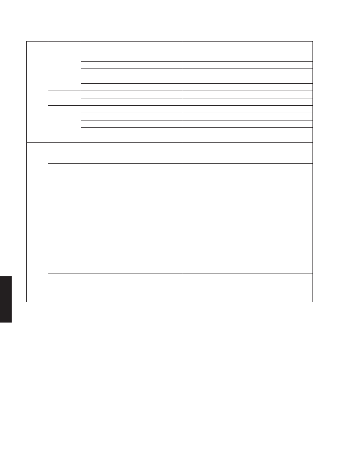
Sound DSP Parameter CINEMA DSP 3D Mode Off / [On]
ECO Auto Power
Function Input Rename Input sources: HDMI1 / HDMI2 / HDMI3 / HDMI4 / HDMI5 / HDMI6 /
SUB-MENU PARAMETER VALUE [INITIAL VALUE]
Panorama [Off] / On
Center Width 0 to 7, [3]
Dimension -3 to +3, [0]
Center Image 0.0 to 1.0, [0.3]
Lipsync Select Manual / [Auto]
Adjustment 0 to 500 ms, [0 ms], 1 ms step
Volume Scale [dB] / 0 to 97
Dynamic Range [Maximum] / Standard / Min/Auto
Max Volume
Initial Volume [Off] / Mute / -80.0 to +16.5 dB, 0.5 dB step
ZoneB Volume [Sync.] / Async.
Timer U, C, R, T, K, A, L, V, H, J models:
Standby
ECO Mode [Off] / On
Input Skip Input sources:
Dimmer -4 to 0 (higher to brighten), [0]
Memory Guard [Off] / On
Remote Color Key [Default] / Input / Program
-30.0 to +15.0 dB / +16.5 dB (Maximum volume), [+16.5 dB], 5.0 dB step
[Off] / 20 minutes / 2 hours / 4 hours / 8 hours /12 hours
B, G, F models:
Off / [20 minutes] / 2 hours / 4 hours / 8 hours / 12 hours
AV1 / AV2 / AV3
AUX
Default: HDMI 1~6 [Auto]
Others [Manual]
Input is possible to 14 characters
Input possible Character type
Capital: A to Z
Small: a to z
Figure: 0 to 9
Symbols: / ( ) = + , - etc.
Space
Preset name select: Blu-ray / DVD / SetTopBox / Game / TV / DVR /
CD / CD-R / Satellite / VCR / Tape / MD / PC /
iPod / HD DVD
HDMI1 / HDMI2 / HDMI3 / HDMI4 / HDMI5 / HDMI6/ AV1 /
AV2 / AV3 / AV4 / AV5 / AV6 / TUNER/ USB /NET/ Bluetooth / AUX
[Off] / On
Input: RED (HDMI2) / GREEN (HDMI6) / YELLOW (AV2) / BLUE (AUX)
Program: RED (MOVIE) / GREEN (MUSIC) / YELLOW (STEREO) /
BLUE (SUR.RECODE)
/ AV4 / AV5 / AV6 / USB / Bluetooh /
RX-V579/TSR-5790
14
Page 15
RX-V579/TSR-5790
MAIN
MENU
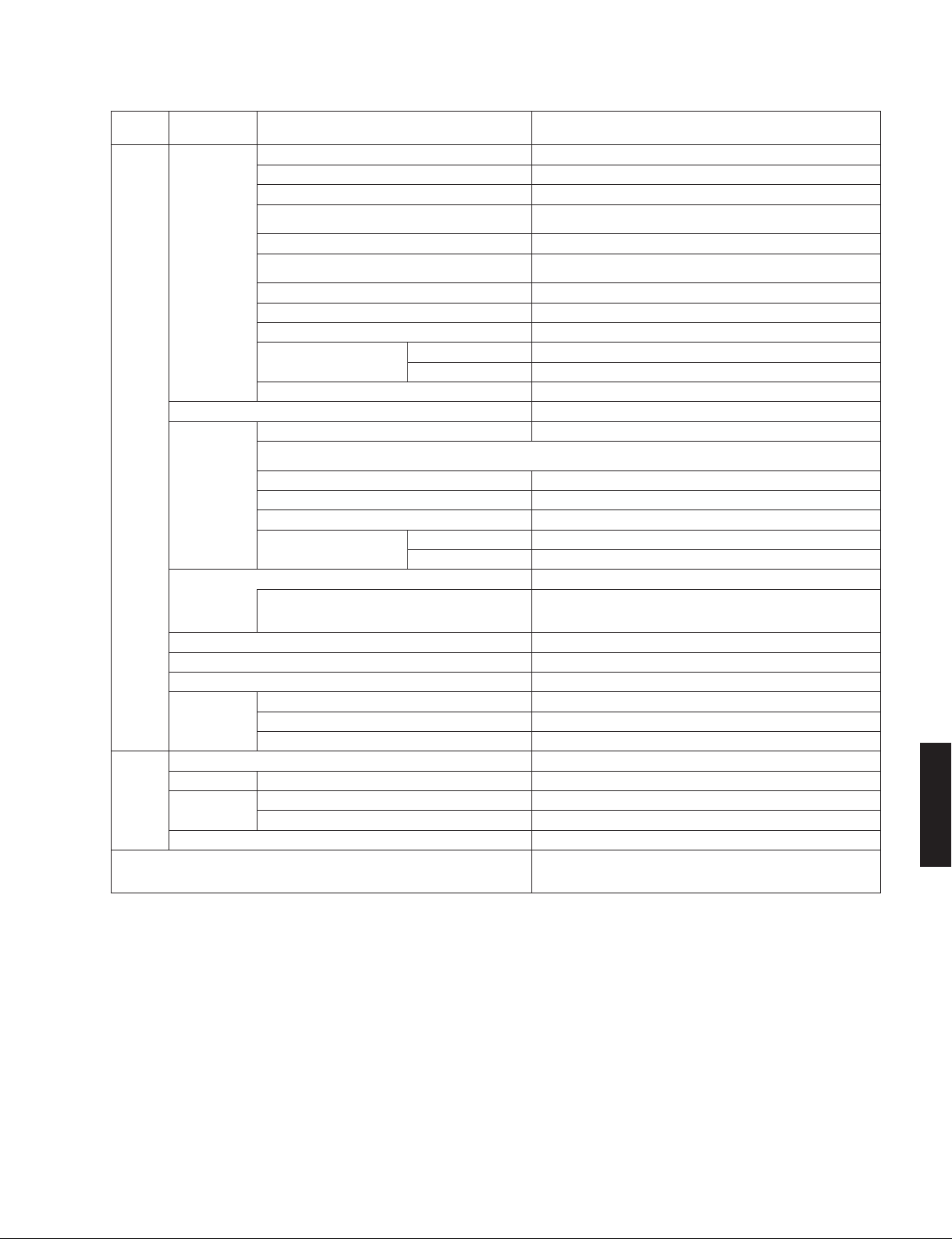
Network Information Status Disconnect / Connect (status of the NETWORK jack)
Bluetooth
Language English (English) / 日本語 (Japanese) / Français (French) /
SUB-MENU PARAMETER VALUE [INITIAL VALUE]
Connection Wired / Wireless (Wi-Fi) / Wireless Direct
SSID xxxx (when connection method is not Wired)
Security None / WPA2-PSK (AES) (Only when connection method is Wireless
MusicCast Network --- / Ready
MAC Address Ethernet : xx:xx:xx:xx:xx:xx
IP Address x
Subnet Mask xxx.xxx.xxx. x
Default Gateway xxx.xxx.xxx. x
DNS Server (Primary) xxx.xxx.xxx. x
(Secondary) xxx.xxx.xxx. x
vTuner (Internet radio) ID xxxxxxxxxxxx
Network Connection Wired / Wireless (Wi-Fi) / Wireless Direct
IP Address DHCP Off / [On]
* The following setting is available only when “DHCP” is set to “Off”.
以下は “DHCP” が “Off” の場合のみ設定可能
IP Address xxx.xxx.xxx. x
Subnet Mask xxx.xxx.xxx. x
ateway xxx.xxx.xxx. x
Default G
DNS Server (Primary) xxx.xxx.xxx. x
(Secondary) xxx.xxx.xxx. x
MAC Address Filter [Off] / On
MAC Address 1–10 xx:xx:xx:xx:xx:xx
DMC Control Disable / [Enable]
Network Standby Off / On / [Auto]
Network Name Input is possible to 15 characters
Network Update Perform Update
Firmware Version x
System ID xxxxxxxx
Bluetooth Off / [On]
Audio Receive Disconnect Terminates the Bluetooth connection
Audio Send Transmitter Off / [On]
Device Search Searches the Bluetooth device
Bluetooth Standby Off / [On]
Direct)
Wi-Fi : xx:xx:xx:xx:xx:xx
xx.xxx.xxx. x
* This setting is available only when “MAC Address Filter” is set to “On”.
“MAC Address Filter” が “On” の場合のみ設定可能
.xx
Deutsch (German) / Español (Spanish) /
Italiano (Italian) / 中文 (Chinese)
Русский
(Russian) /
RX-V579/TSR-5790
15
Page 16
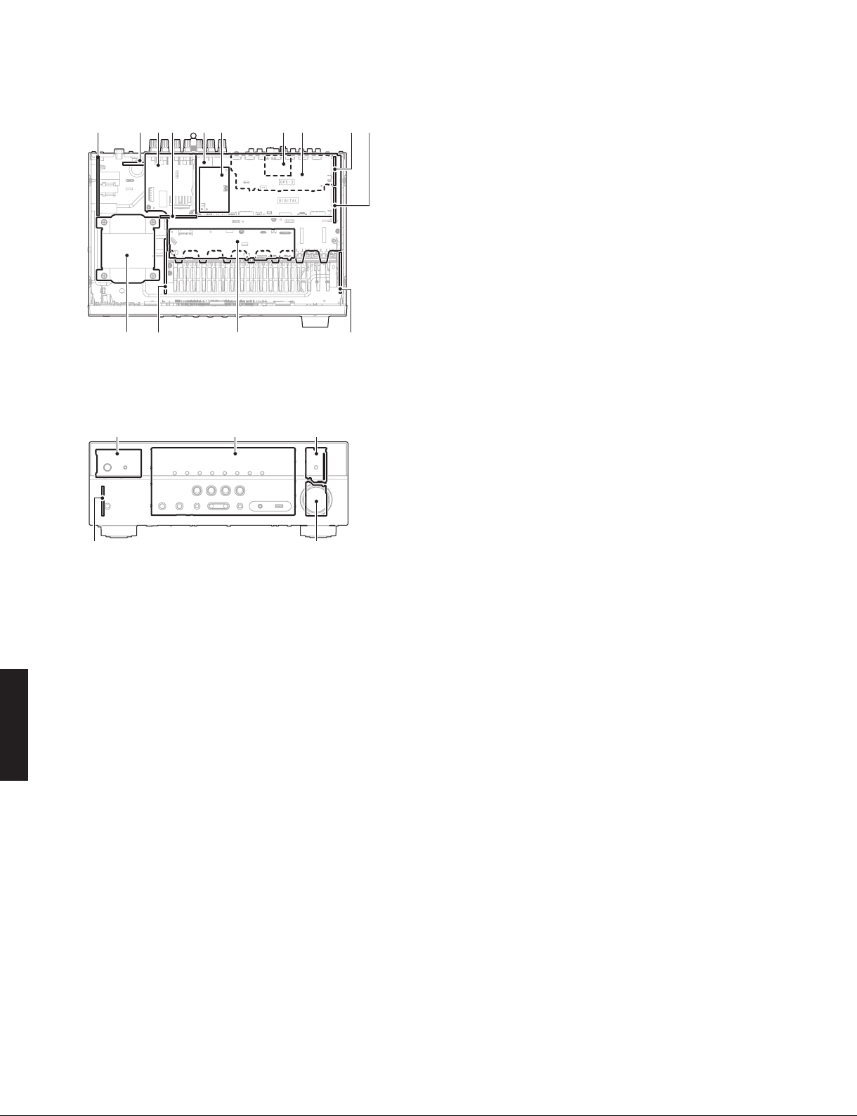
RX-V579/TSR-5790
■ INTERNAL VIEW
Top view
1 2 5 6
Front view
3 4
7 8
ln
p qo
9
j
a
OPERATION (2) P.C.B.
b
MAIN (4) P.C.B. (R, V models)
c
MAIN (1) P.C.B.
d
OPERATION (8) P.C.B.
e
DIGITAL P.C.B.
f
Network Module
g
AM/FM TUNER
h
OPERATION (3) P.C.B.
i
MAIN (3) P.C.B.
j
MAIN (2) P.C.B.
km
k
MAIN (5) P.C.B.
l
OPERATION (4) P.C.B.
m
N (6) P.C.B.
MAI
n
POWER TRANSFORMER
o
OPERATION (5) P.C.B.
p
OPERATION (1) P.C.B.
q
OPERATION (10) P.C.B.
r
OPERATION (6) P.C.B.
s
OPERATION (7) P.C.B.
s
■ SERVICE PRECAUTIONS / サービス時の注意事項
Safety measures
• Some internal par ts in this product contain high
voltages and are dangerous.
RX-V579/TSR-5790
Be sure to take safety measures during servicing, such
as wearing insulating gloves.
• Note t h a t th e ca p a citors in d i c a ted below ar e
dangerous even after the power is turned off because
an elec tric char ge rema ins and a high volt age
continues to exist there.
Before starting a
resistor (5 k-ohms/10 W) to the terminals of each
capacitor indicated below to discharge electricity.
The time required for discharging is about 30 seconds
per each.
C2185 and C2186 on MAIN (1) P.C.B.
C5419 on OPERATION (2) P.C.B.
For details, refer to “PRINTED CIRCUIT BOARDS”.
r
ny repair work, connect a discharging
安全対策
• この製品の内部には高電圧部分があり危険です。修理
の際は、絶縁性の手袋を使用するなどの安全対策を行っ
てください。
• 下記のコンデンサには電源を OFF にした後も電荷が残
り、高電圧が維持されており危険です。
修理作業前に放電用抵抗(5 k Ω /10 W)を下記の各コ
ンデンサの端子間に接続して放電してください。
放電所用時間は各々約 30 秒間です。
MAIN(1)P.C.B. の C2185、C2186
OPERATION(2)P.C.B. の C5419
詳しくは “PRINTED CIRCUIT BOARDS” を参照してく
ださい。
16
Page 17
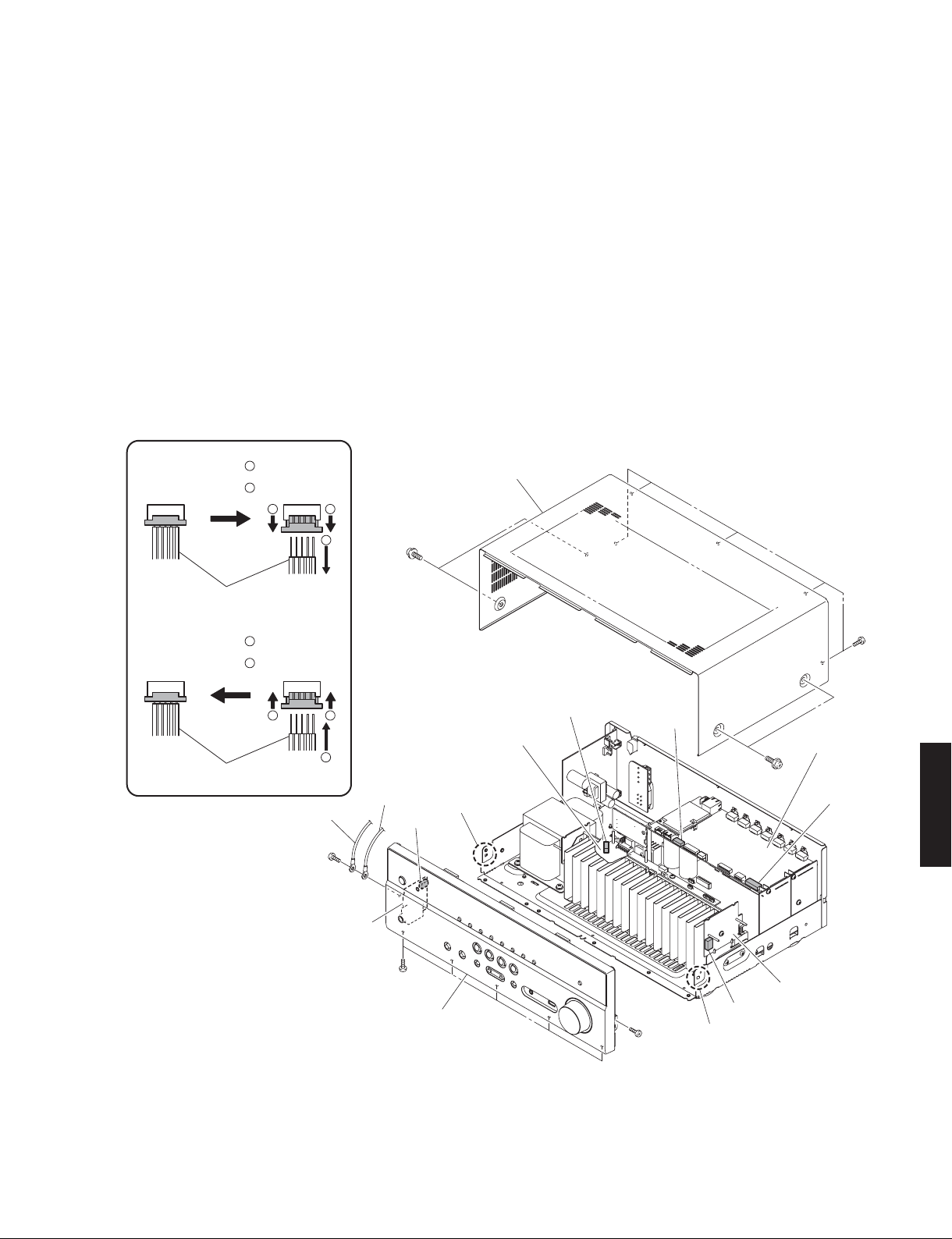
■ DISASSEMBLY PROCEDURES / 分解手順
(Remove parts in the order as numbered.)
Disconnect the power cable from the AC outlet.
(番号順に部品を外してください。)
RX-V579/TSR-5790
AC 電源コンセントから、電源コードを抜いてください。
1. Removal of Top Cover
a. Remove 4 screws (1) and 5 screws (2). (Fig. 1)
b. Lift the rear of the top cover to remove it. (Fig. 1)
2. Removal of Front Panel Unit
a. Remove 7 screws (3), and remove W4501 and
W4761. (Fig. 1)
b. Remove CB21, CB351, CB477 and CB953. (Fig.1)
c. Unlock and rem
d. Release 2 hooks on both ends and remove the front
panel unit. (Fig. 1)
Connected
接続
Connected
接続
ove CB525. (Fig. 1)
Remove CB525
ケーブル
Connect CB525
Cable
Unlock the connector
1
コネクターロック解除
Remove the cable
2
ケーブルを外す
Lock the connector
1
コネクターロック
Insert the cable
2
ケーブルを差し込む
1 1
2
①
1. トップカバーの外し方
a. 1のネジ 4 本、2のネジ 5 本を外します。(Fig. 1)
b. トップカバーの後部を持ち上げ、外します。(Fig. 1)
2. フロントパネルユニットの外し方
a. 3のネジ 7 本を外 し、W4501、W4761 を外します。
(Fig.1)
b. CB21、CB351、CB477、CB953 を外します。(Fig.1)
c. ロックを外し、CB525 を外します。(Fig. 1)
d. フック 2 箇所を外し、フロントパネルユニットを外し
ます。(Fig. 1)
Top cover
トップカバー
②
1 1
Cable
ケーブル
OPERATION (7) P. C.B.
W4761
③
CB525
OPERATION (4) P. C.B.
2
CB953
DIGITAL P. C.B.
RX-V579/TSR-5790
①
W4501
Hook
フック
CB21
CB477
③
Front panel unit
フロント パネルユニッ ト
③
Hook
フック
MAIN (5) P. C.B.
CB351
Fig. 1
17
Page 18
RX-V579/TSR-5790
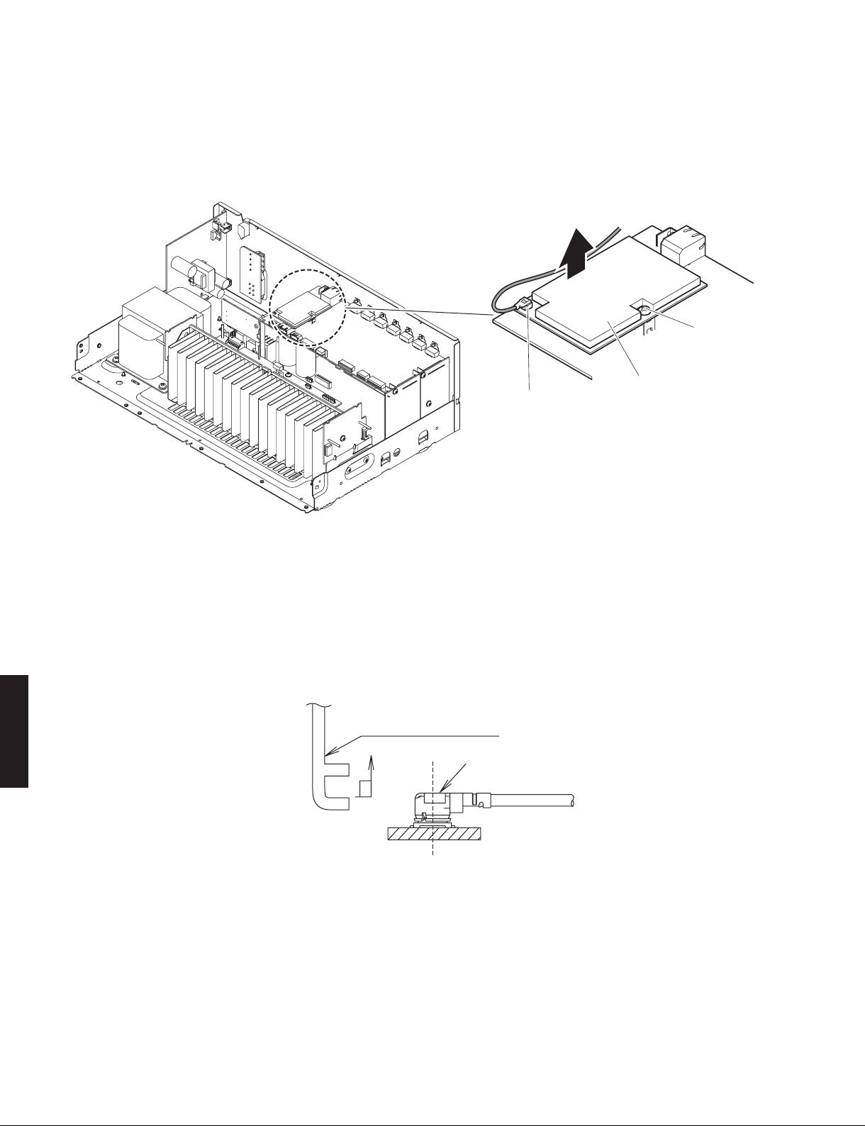
3. Removal of Network Module
a. The Wireless LAN Antenna Connector is removed by
using MHF Connector Remover. (Fig. 2)
b. Remove screw (4). (Fig. 2)
c. Remove the Network Module to upward.
3. ネットワークモジュールの外し方
a. MHF コネクター挿抜工具を使い、無線 LAN アンテナ
コネクターを外します。(Fig. 2)
b. 4のネジ 1 本を外します。(Fig. 2)
c. ネットワークモジュールを上方向に取り外します。
Network module
Wireless LAN
Antenna Connector
無線LAN アンテナ
コネクター
Fig. 2
ネットワークモジュール
④
CAUTION !
• To remove the Wireless LAN Antenna Connector, use
the special MHF Connector Remover. Hook the tip
of this tool on the cover of the Wireless LAN Antenna
Connector and pull it straight in the direction of t
engaging axis of the Wireless LAN Antenna Connector.
(Fig. 3)
Special removing tool
ZK708100: MHF Connector Remover
RX-V579/TSR-5790
• The Wireless LAN Antenna Connector should only be
plugged back to the Network Module after it has been
installed back onto the DIGITAL P.C.B.
• When plugging the Wireless LAN Antenna Connector
back to the Network Module, make sure to hold it and
insert it vertically using the MHF Co
Make sure not to insert the Wireless LAN Antenna
Connector at a sharp angle as it may break.
• The Wireless LAN Antenna Connector can be inserted
and removed up to 5 times only.
he
MHF Connector Remover /
MHF コネクター挿抜工具
nnector Remover.
注意!
• 無線 LAN アンテナコネクターを外す場合は、専用の
MHF コネクター挿抜工具の先端部を無線 LAN アンテ
ナコネクターふた部に引っかけ、無線 LAN アンテナコ
ネクターの嵌合軸に合わせ垂直
に引き抜いてください。
(Fig. 3)
専用の MHF 挿抜工具
ZK708100:MHF コネクター挿抜工具
Wireless LAN Antenna Connector /
無線 LAN アンテナコネクター
Fig. 3
• 無線 LAN アンテナコネクター挿入時は、ネットワーク
モジュールを DIGITAL P.C.B. に取り付けた状態で行っ
てください。
• 無線 LAN アンテナコネクター挿入時は、MHF コネク
ター挿抜工具を使って無線 LAN アンテナコネクターを
垂直に挿入してください。極端に斜めから挿入すると、
故障の原因になります。
• 無線 LAN アンテナコネクターの挿抜は 5 回までとして
ください。
18
Page 19
RX-V579/TSR-5790
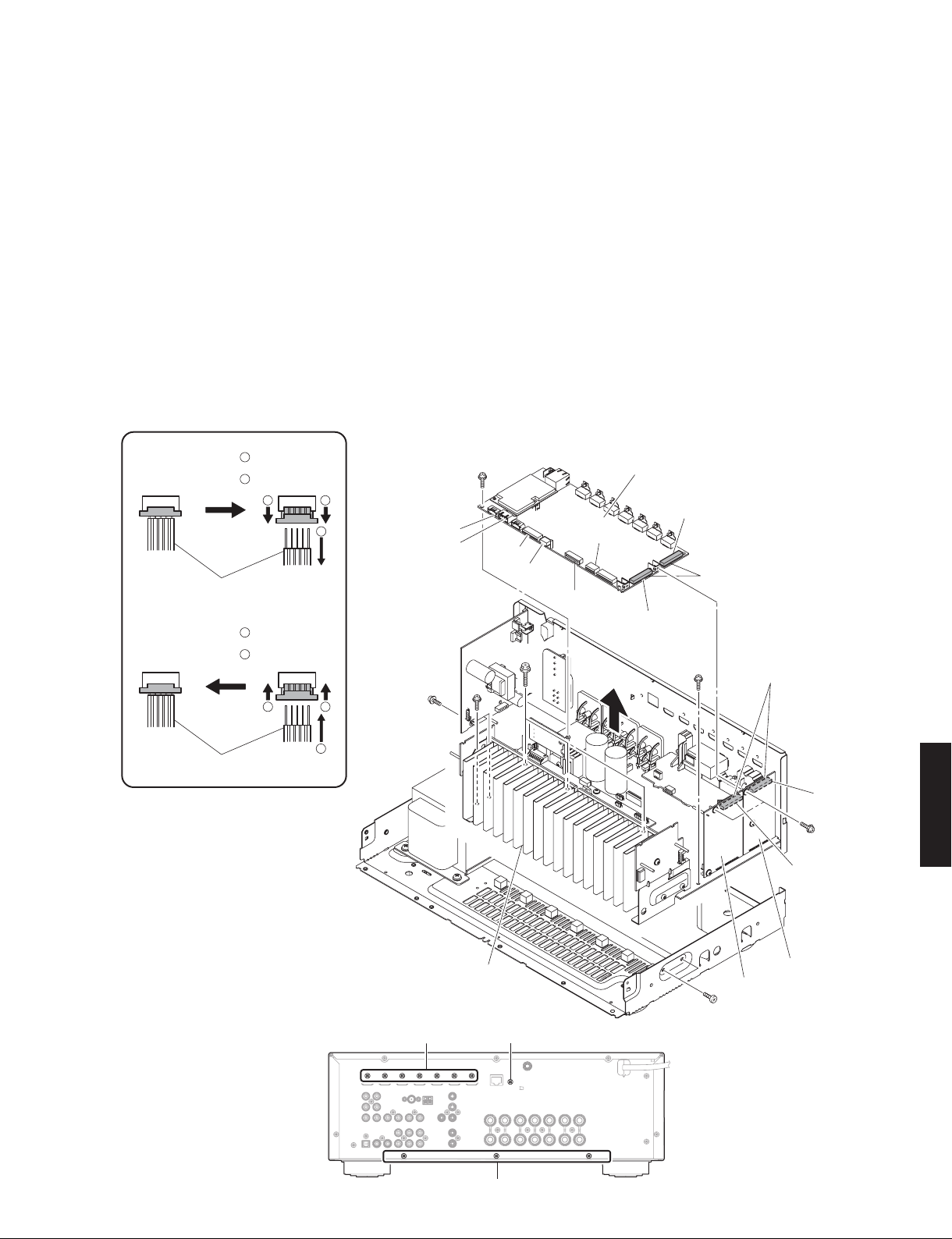
4. Removal of DIGITAL P.C.B.
a. Remove 1 screw (5) and 7 screws (6). (Fig. 5)
b. Remove 3 screws (7). (Fig. 4)
c.
Remove CB22, CB23, CB26, CB27 and CB81. (Fig. 4)
d. Unlock and remove CB25. (Fig. 4)
e. Remove the Antenna Cable tied to the DIGITAL P.C.B.
f. Remove the DIGITAL P.C.B. which is connected
directly to the MAIN (2) P.C.B. and MAIN (3) P.C.B.
with board-to-board connectors. (Fig. 4)
5. Removal of AMP Unit
a. Remove 3 screws (8), 4 screws (9) and 2 screws
(j). (Fig. 4)
b. Remove 3 screws (k). (Fig. 5)
c. Remove the amp unit. (Fig. 4)
Connected
接続
Connected
接続
Remove CB25
Cable
ケーブル
Connect CB25
Unlock the connector
1
コネクターロック解除
Remove the cable
2
ケーブルを外す
1 1
Lock the connector
1
コネクターロック
Insert the cable
2
ケーブルを差し込む
1 1
2
CB27
CB81
⑨
4. DIGITAL P.C.B. の外し方
a. 5のネジ 1 本、6のネジ 7 本を外します。(Fig. 5)
b. 7のネジ 3 本を外します。(Fig. 4)
c.
CB22、CB23、CB26、CB27、CB81 を外します。(Fig. 4)
d. ロックを外し、CB25 を外します。(Fig. 4)
e. DIGITAL P.C.B に結束されているアンテナ同軸ケーブ
ルを外します。
f. DIGITAL P.C.B. を外します。ただし、DIGITAL P.C.B.
は MAIN(2)P.C.B.、MAIN(3)P.C.B. に基板対基板
コネクタ
ーで直接接続されています。(Fig. 4)
5. アンプユニットの外し方
a. 8のネジ 3 本、9のネジ 4 本、jのネジ 2 本を外し
ます。(Fig. 4)
b. kのネジ 3 本を外します。(Fig. 5)
c. アンプユニットを外します。(Fig. 4)
⑦
CB22
CB23
⑧
⑨
CB26
CB25
DIGITAL P. C.B.
CB62
CB63
Board-to-board connectors
基板対基板コネクター
Board-to-board connectors
⑨
基板対基板コネクター
Cable
ケーブル
Fig. 5
2
Fig. 4
AMP unit
アンプユニット
⑥⑤
⑪
RX-V579/TSR-5790
CB271
⑦
CB251
MAIN (3) P. C.B.
MAIN (2) P. C.B.
⑩
19
Page 20
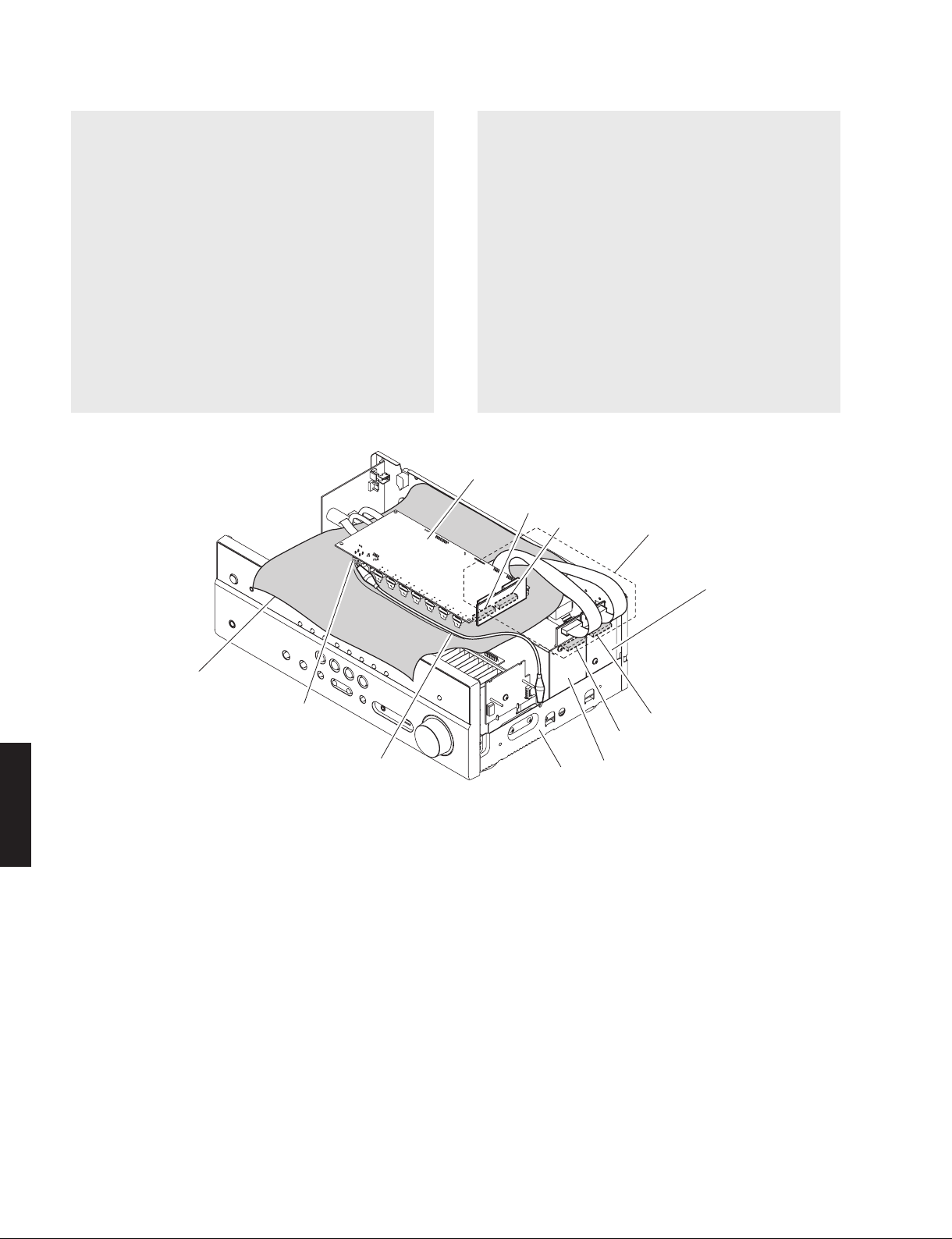
RX-V579/TSR-5790
When checking the DIGITAL P.C.B.:
• Put the rubber sheet and cloth over this unit, and
place the DIGITAL P.C.B. on them. (Fig. 6)
• Connect ST952 on DIGITAL P.C.B. to the chassis with
a ground lead. (Fig. 6)
• Reconnect all cables (connectors) that have been
disconnected. Be sure to use the P.C.B. CHECKING
JIG (Part No. ZG780000) to connect between the
following connectors.
CB62 on DIGITAL P.C.B. – CB
P.C.B.
CB63 on DIGITAL P.C.B. – CB251 on MAIN (2)
P.C.B.
• When connecting the flexible flat cable, be careful
with polarity.
271 on MAIN (3)
DIGITAL P.C.B. をチェックする場合には:
• 本機の上にゴムシートと布を敷き、その上に DIGITAL
P.C.B. を置きます。(Fig. 6)
• DIGITAL P.C.B. の ST952 の ア ー ス を リ ー ド 線 で
シャーシに接続してください。(Fig. 6)
• 外したケーブル(コネクター)をすべて接続しま
す。ただし下記のコネクター間を接続するには P.C.B.
チェック用ジグ(部品番号 : ZG780000)を使用して
ください。
DIGITAL P.C.B. の CB62 ‒ MAIN (3) P.C.B. の
CB271
DIGITAL P.C.B. の CB63 ‒ MAIN (2) P.C.B. の
CB251
• フラットケーブルを接続する際、極性に注意してく
ださい。
DIGITAL P.C.B.
CB62
CB63
P.C.B. CHECKING JIG
P.C.B. チェック用ジグ
RX-V579/TSR-5790
Rubber sheet and cloth
ゴムシートと布
ST952
Ground lead
アース線
Fig. 6
Chassis
シャーシ
MAIN (3) P.C.B.
CB271
CB251
MAIN (2) P.C.B.
20
Page 21
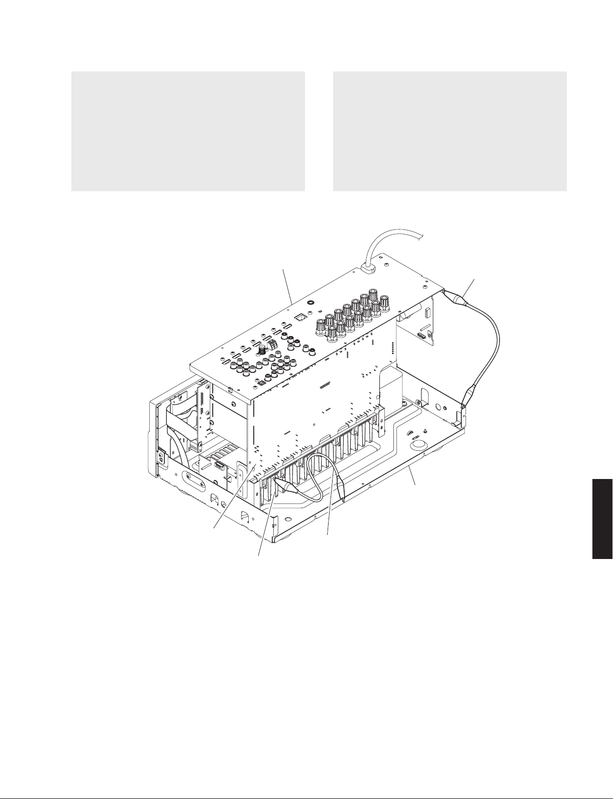
RX-V579/TSR-5790
When checking the MAIN (1) P.C.B.:
• Place the P.C.B.s (with rear panel) upright. (Fig. 7)
• Connect the heatsink and rear panel to the chassis
with a ground lead or the like. (Fig. 7)
• Reconnect all cables (connectors) that have been
disconnected.
• When connecting the flexible flat cable, be careful
with polarity.
Rear panel
リアパネル
MAIN(1)P.C.B. をチェックする場合には:
• リアパネル と一緒に P.C.B. を立ち上げて置 きます。
(Fig. 7)
• ヒートシンク、リアパネルをリード線等でシャーシ
に接続してください。(Fig. 7)
• 外したケーブル(コネクター)をすべて接続します。
• フラットケーブルを接続する際、極性に注意してく
ださい。
Ground lead
アース線
MAIN (1) P.C.B.
RX-V579/TSR-5790
Chassis
シャーシ
Ground lead
アース線
Heatsink
ヒートシンク
Fig. 7
21
Page 22

RX-V579/TSR-5790
■ UPDATING FIRMWARE / ファームウェアのアップデート
When the following parts are replaced, the firmware must
be updated to the latest version.
DIGITAL P.C.B.
IC2 on DIGITAL P.C.B.
IC42 on DIGITAL P.C.B.
IC902 on DIGITAL P.C.B.
IC903 on DIGITAL P.C.B.
Network module
下記の部品を交換した場合、ファームウェアを最新バー
ジョンにアップデートする必要があります。
DIGITAL P.C.B.
DIGITAL P.C.B. の IC2
DIGITAL P.C.B. の IC42
DIGITAL P.C.B. の IC902
DIGITAL P.C.B. の IC903
ネットワークモジュール
● Confirmation of firmware version
Before and after updating the firmware, check the
firmware version by using the self-diagnostic function
menu.
Start up the se
ROM VERSION/CHECKSUM” menu.
Using the sub-menu, have the firmware version
displayed, and note them down.
(For details, refer to “SELF-DIAGNOSTIC FUNCTION”)
* Whe n the firmware version is different from
written one after updating, perform the updating
procedure again from the beginning.
lf-diagnostic function and select “S4.
● Initializing the back-up IC
(EEPROM: IC22 on DIGITAL P.C.B.)
After updating the firmware, the back-up IC MUST
be initialized by the following procedure store the
setting information (soundfield parameters, system
memory and tuner presetting, etc.) properly.
Start up the self-diagnostic function and select “S3.
FACTORY PRESET” menu.
(For details, refer to “SELF-DIAGNOSTIC FUNCTION”)
Select “PRESET RSRV”, press the “z” (Power) key to
turn off the power once and
Then the back-up IC is initialized.
turn on the power again.
● ファームウェアのバージョンの確認
ファームウェアのアップデートの前後に、ファーム
ウェアのバージョンをダイアグで確認します。
ダイアグを起動し、“S4. ROM VERSION/CHECKSUM”
メニューを選択します。
サブメニューでファームウェアのバージョンを表示
し、それらを書きとめます。
(詳細は “ ダイアグ ” を参照してください。)
※ アップデート後、ファームウェアのバージョンが
書き込
まれたものと異なる場合、アップデートの
操作を最初からやり直してください。
● バックアップ IC の初期化
(EEPROM:DIGITAL P.C.B. の IC22)
ファー ムウェアの アップデート後、設定 情報(音
場プログラムのパラメーターやシステムメモリー、
チューナープリセット等)を正常に保存するために、
下記の方法でバックアップ IC を初期化する必要があ
ります。
本機のダイ ア グ を 起動し、“S3. FACTORY PRESET”
メニューを選択します。
(詳細は “ ダイアグ ” を参照してください。)
“PRESET RSRV” を選択し、“z”(電源)キーを押し
て電源を一度きってから、もう一度電源を入れると
バックアップ IC が初期化されます。
● Required Tools
RX-V579/TSR-5790
• USB storage device
• Firmware ........................................R0371-xxxx.bin
● Preparation
1. Download the latest firmware from the specified
download source to the folder of the PC.
2. Copy the latest firmware from the PC to the root
folder of the USB storage device.
Note:
22
When the lates t firmw are is copi ed to a
subfolde
update will not proceed.
r of the USB storage device, the
● 必要なツール
・ USB フラッシュメモリー
・ ファームウェア ..............................R0371-xxxx.bin
● 準備
1. 指定のダウンロード先から、最新のファームウェ
アを PC のフォルダへダウンロードしてください。
2. PC から USB フラッシュメモリーのルートフォル
ダへ最新のファームウェアをコピ
注意 : 最新のファームウェアをサブフォルダにコピー
した場合、書き込みはできません。
ーします。
Page 23
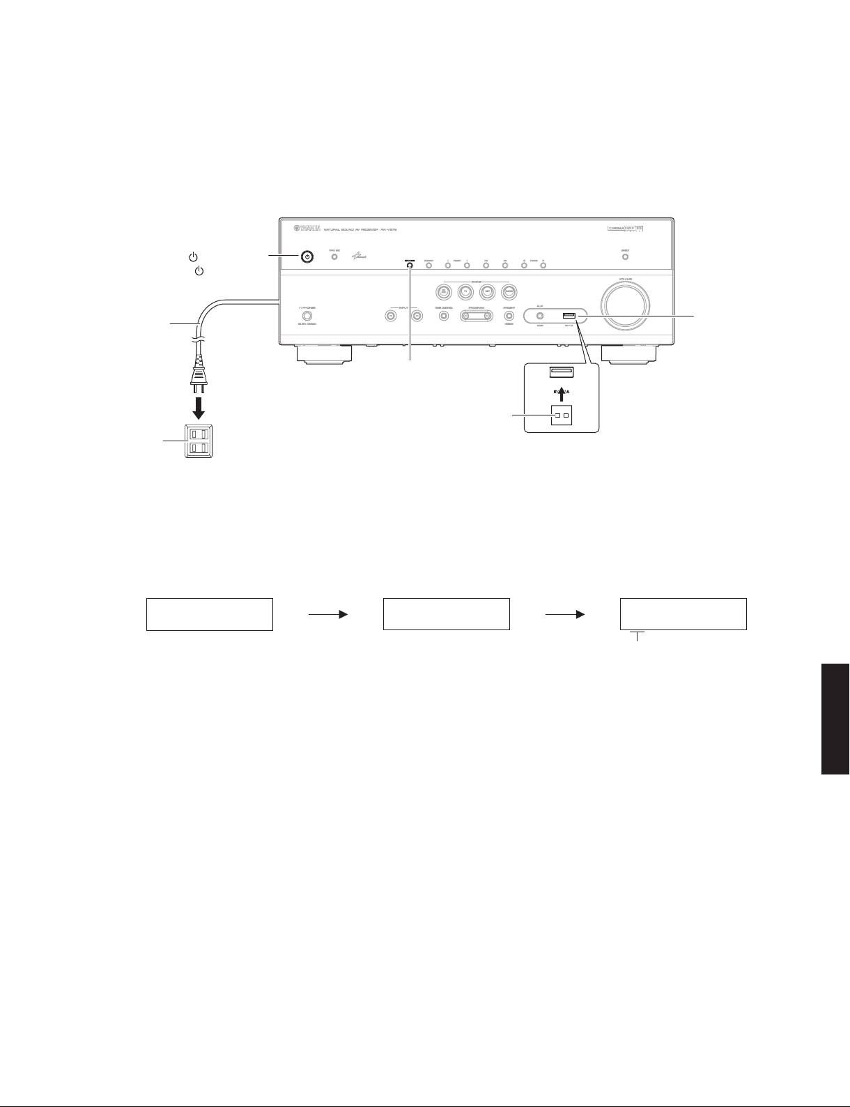
RX-V579/TSR-5790
● Operation Procedures
1. Disconnect the power cable from the AC outlet.
2. Insert the USB storage device to the USB jack.
(Fig. 1)
3. While pressing the “INFO” key, connect the power
cable to the AC outlet. (Fig. 1)
" " (Power) key
""(電源)キー
Power cable
電源コード
AC outlet
ACコンセント
4. The USB UPDATE mode is activated and “USB
UPDATE” is displayed. Writing of the firmware
starts automatically. (Fig. 2)
● 操作手順
1. 電源コードを AC コンセントから抜きます。
2. USB 端子に USB フラッシュメモリーを差し込み
ます。(Fig. 1)
3. “INFO” キーを押しながら、電源コードを AC コン
セントに接続します。(Fig. 1)
USB jack
USB 端子
"INFO" key
“INFO” キー
USB storage device
USB フラッシュメモリー
Fig. 1
4. USB UPDATE モードが起動し、“USB UPDATE” が
表示されて、ファームウェアの書き込みが自動的
に開始されます。(Fig. 2)
Writing is started. / 書き込み開始 Writing being executed. / 書き込み中
USB UPDATE VERIFYING... Sx-X:XX%
S1: NET (Network module) section
S2: MAIN (IC21 on DIGITAL P.C.B.) section
S3: DSP1 (IC42 on DIGITAL P.C.B.) section
S4: DSP2 section (Not available)
S5: OSD (IC2 on DIGITAL P.C.B.) section
S6: HDMI (IC902, IC903 on DIGITAL P.C.B.) section
xxxx” が表示された場合、“ エラーメッセージ一覧 ”
で原因を参照し、アップデートの操作を最初から
やり直してください。
* If “ERROR! xxxx” is displayed during writing of
the firmware, re
fer to “List of Error Messages” to
determine the cause and perform the updating
procedure again from the beginning.
Fig. 2
※ フ ァ ームウ ェ アの書 き 込みの 途 中で “ERROR!
RX-V579/TSR-5790
23
Page 24
RX-V579/TSR-5790
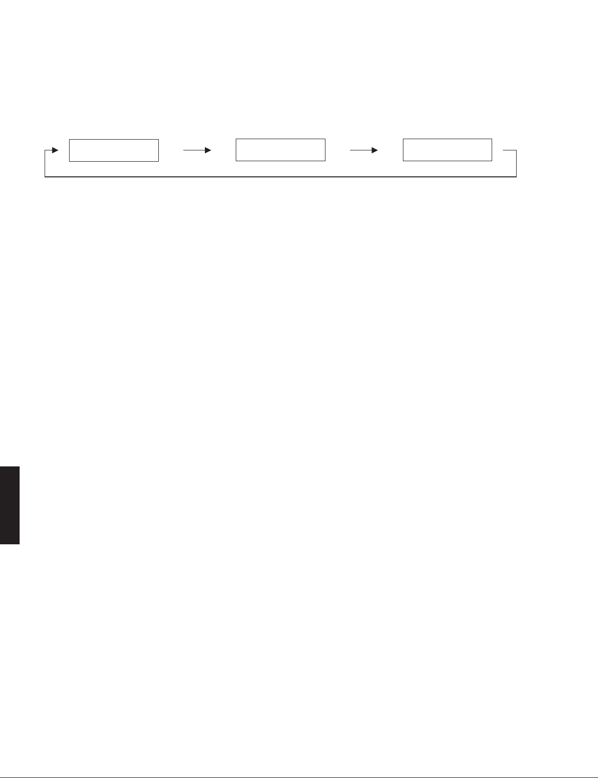
5. W hen writing of the firmware is completed,
“ U PDAT E S UC C ES S ”, “ PL E AS E .. . ” a n d
“POWEROFF!” are displayed repeatedly. (Fig. 3)
Writing is completed. / 書き込み完了
5. フ ァ ー ム ウ ェア の書 き込 み 完 了 後、“UPDATE
SUCCESS”、“PLEASE...”、“POWEROFF!” が 繰 り
返し表示されます。(Fig. 3)
UPDATE SUCCESS PLEASE... POWEROFF!
Fig. 3
6. Press the “z” (Power) key to turn off the power.
(Fig. 1)
7. Remove the USB storage device from the USB
jack. (Fig. 1)
8.
Start up the self-diagnostic function and check that
the firmware version is the same as written one.
(For details, refer to “Confirmation of firmware
version”)
6. “z”(電源)キーを押して電源を切り ます。(Fig. 1)
7. USB 端子から USB フラッシュメモリーを抜きま
す。(Fig. 1)
8. ダイアグを起動し、ファームウェアのバージョン
が、書き込まれたものと同じであることを確認し
ます。
(詳細は “ ファームウェアのバージョンの確認 ” を
参照してください。)
RX-V579/TSR-5790
24
Page 25
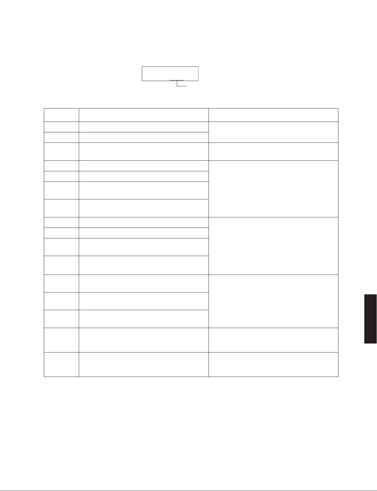
List of Error Messages / エラーメッセージ一覧
Display / 表示
ERROR! xxxx
RX-V579/TSR-5790
Error number / エラー番号
Error Number
エラー番号
0001 Microprocessor clearing error / マイコン消去エラー
0002 Microprocessor writing error / マイコン書き込みエラー
Microprocessor checksum error
0004
マイコンチェックサムエラー
0008 DSP1 status port error / DSP1 ステータスポートエラー
0010 DSP1 checksum error / DSP1 チェックサムエラー
DSP1 data reception time out
0020
DSP1 データ受信タイムアウト
DSP1 checksum calculation time out
0040
DSP1 チェックサム計算タイムアウト
0080 DSP2 status port error / DSP2 ステータスポートエラー
0100 DSP2 checksum error / DSP2 チェックサムエラー
DSP2 date reception time out
0200
DSP2 データ受信タイムアウト
DSP2 checksum
0400
DSP2 チェックサム計算タイムアウト
OSD Flash ROM clearing error
0800
OSD Flash ROM 消去エラー
OSD Flash ROM writing error
1000
OSD Flash ROM 書き込みエラー
OSD Flash ROM checksum error
2000
OSD Flash ROM チェックサムエラー
HDMI1 Flash ROM related error
4000
HDMI1 Flash ROM 関連エラー
HDMI2 Flash ROM related error
8000
HDMI2 Flash ROM 関連エラー
Error Message
エラーメッセージ
calculation time out
Cause
原因
Microprocessor failure
マイコン不良
Microprocessor failure / Disagreement to checksum
マイコン不良/チェックサムの不一致
DSP1 failure /
Malfunction of communication with microprocessor
DSP1 不良/マイコンと
DSP2 failure /
Malfunction of communication with microprocessor
DSP2 不良/マイコンとの通信異常
OSD Flash ROM failure /
Malfunction of communication with microprocessor
OSD Flash ROM 不良/マイコンとの通信異常
HDMI1 failure /
Malfunction of communication with
HDMI1 不良/マイコンとの通信異常
HDMI2 failure /
Malfunction of communication with microprocessor
HDMI2 不良/マイコンとの通信異常
の通信異常
(Not available)
microprocessor
RX-V579/TSR-5790
* The error number is displayed in the 4-digit hexadecimal notation.
エラー番号は 4 桁の 16 進数で表示されます。
* The error numbers are added when a multiple number of errors occur at the same time.
エラー番号は同時に複数のエラーが発生すると、加算されます。
Example / 例 If errors
エラー番号の “0002” と “0008” のエラーが同時に発生すると、エラー番号は “000A” と表示されます。
by the error number “0002” and “0008” occur at the same time, the error number will be displayed as “000A”.
25
Page 26
RX-V579/TSR-5790
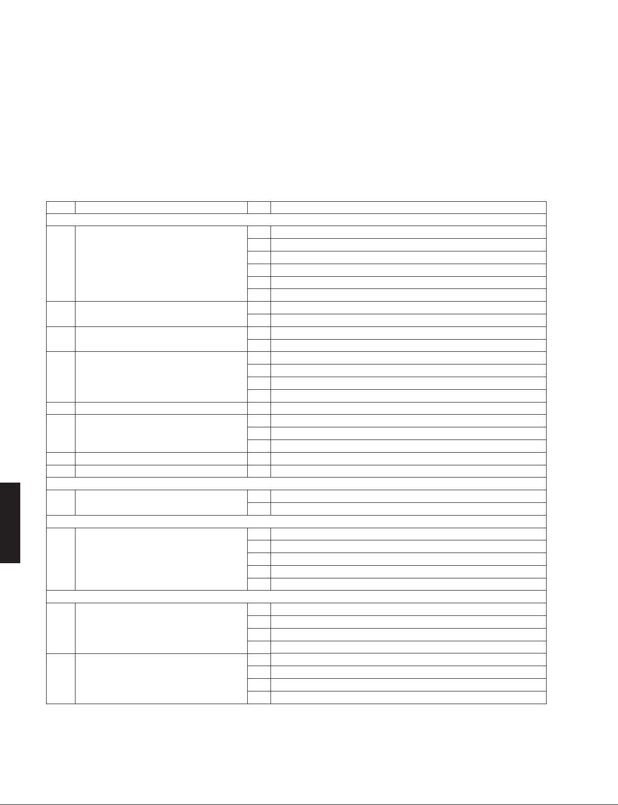
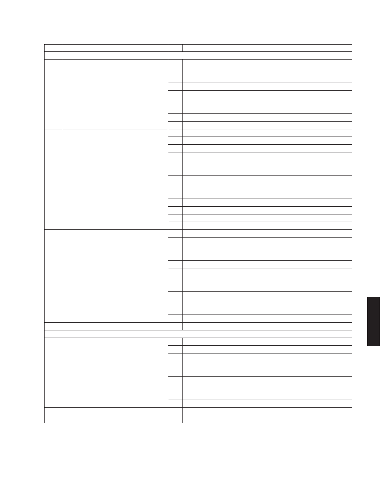
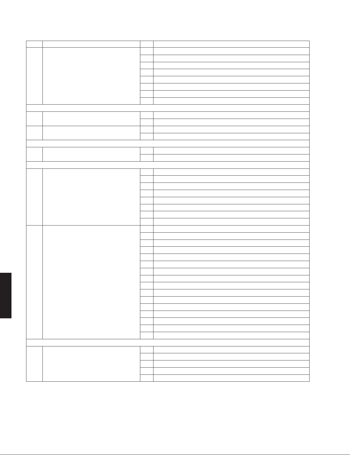
■ SELF-DIAGNOSTIC FUNCTION / ダイアグ(自己診断機能)
This unit has self-diagnostic functions that are intended
for inspection, measurement and location of faulty point.
Each item has a main menu, each of which has submenu
items.
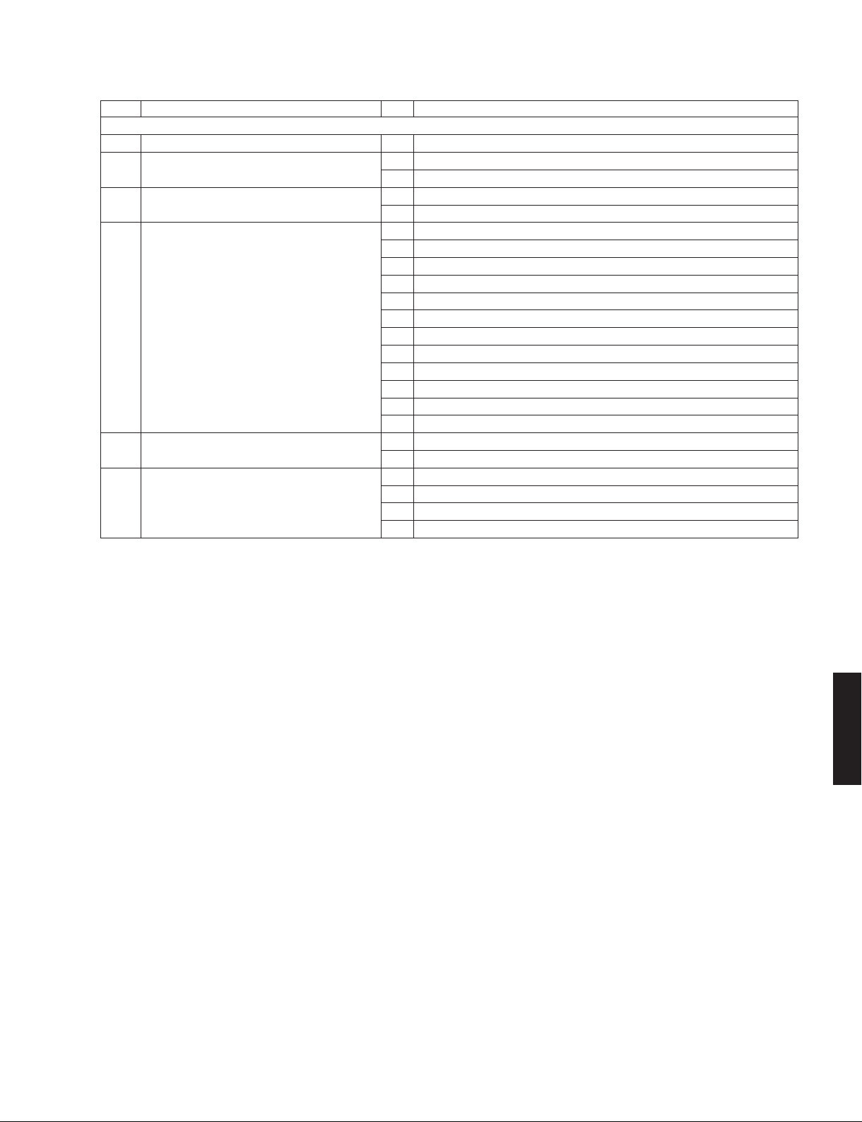
Listed in the table below are main menu items and
submenu items.
Note:
Some of the menu items listed below may not apply
to the models covered in this service manual.
No. Main menu No. Sub-menu
A:
Audio system / オーディオ系
A1 DSP AUDIO 1 DSP MARGIN
A2 DIRECT AUDIO 1 ANALOG DIRECT
A3 HDMI AUDIO 1 HDMI AUTO
A4 SPEAKERS SET 1 FULL MUTE
A5 MIC CHECK 1 MIC ROUTE CHECK
A6 INVALID ITEM
(Not for service / サービスでは使用しません )
A7 DIR PLL 1 DIR PLL
A8 MANUAL TEST 1 TEST ALL
H:
HDMI / HDMI
H1 INVALID ITEM
(Not for service / サービスでは使用しません )
D:
Display system / 表示系
D1 FL CHECK 1 FL CHECK
RX-V579/TSR-5790
U:
Universal system / 特殊端子系
U1 USB 1 USB FRONT 1 TRACK
U2 USB COMPLIANCE TEST
(Not for service / サービスでは使用しません )
本機には、検査、測定、不良個所の発見を目的にした
イアグ(自己診断機能)があります。
ダイアグには項目別にメインメニューがあり、そのそれ
ぞれにサブメニューがあります。
下表はダイアグメニュー一覧です。
注意: 以下のメニュー項目の一部は、このサービスマニュ
アルに記載されているモデルに適用されない場合
があります。
2 DSP NON MARGIN
3 DSP FULL CENTER
4 DSP FULL SURROUND
5 DSP FULL SURROUND BACK
6 DSP FULL SUBWOOFER
2 INVALID ITEM
2 ARC
2 BI-AMP
3 AC_B : HIGH
4 AC_B : LOW
1 INVALID ITEM
2 INVALID ITEM
3 INVALID ITEM
1 INVALID ITEM
2 INVALID ITEM
2 ALL SEGMENT OFF
3 ALL SEGMENT ON
4 CHECK PATTERN 1
5 CHECK PATTERN 2
2 USB BOOT
3 INVALID ITEM
4 USB AUDIO
1 TEST SEO NAK
2 TEST J
3 TEST K
4 TEST PACKET
ダ
(Not for service / サービスでは使用しません )
(Not for service / サービスでは使用しません )
(Not for service / サービスでは使用しません )
(Not for service / サービスでは使用しません )
(Not for service / サービスでは使用しません )
26
Page 27
No. Main menu No. Sub-menu
N:
Network system / ネットワーク系
N1 NETWORK 1 IP ADDRESS CHECK
2 MAC ADDRESS CHECK
3 LINE NOISE 100 MDI
4 LINE NOISE 100 MDIX
5 LINE NOISE 10 MDI
6 LINE NOISE 10 MDIX
(Not for service / サービスでは使用しません )
(Not for service / サービスでは使用しません )
(Not for service / サービスでは使用しません )
(Not for service / サービスでは使用しません )
7 LINK CHECK
8 EXT TEST
10 PING
N2 WIFI
(Not for service / サービスでは使用しません )
1 WIFI ON JIG01
2 WIFI ON JIG02
3 WIFI
ON JIG03
4 WIFI ON JIG04
5 WIFI ON JIG05
6 WIFI ON JIG06
7 WIFI ON JIG07
8 WIFI ON JIG08
9 WIFI ON JIG09
10 WIFI ON JIG10
11 WIFI OFF
12 WIFI MAC ADDRESS
13 WIFI RF TEST
N3 BLUETOOTH
(Not for service / サービスでは使用しません )
1 BT VERSION
2 BT ADDRESS
3 PLAYBACK
N4 NET AUDIO 1 LOOPBACK 0 TEST
2 LOOPBACK 1 TEST
3 LOOPBACK 2 TEST
4 LOOPBACK 3 TEST
5 NET AUDIO PLAYBACK 0 TEST
6 NET AUDIO PLAYBACK 1 TEST
7 NET AUDIO PLAYBACK 2 TEST
8 NET AUDIO PLAYBACK 3 TE
9 LOOPBACK ZONE DAC TEST
ST
(Not for service / サービスでは使用しません )
N5 SPI LOOPBACK 1 SPI LOOPBACK TEST
C:
Communication system / 通信・バスライン系
C1 ACCESS CHECK 1 ALL
2 MCPU OSD
3 OSD HDMI
4 VIDEO I/F
5 DIR BUS
6 DSP BUS
7 EEPROM
8 TUNER
9 INVALID ITEM
(Not for service / サービスでは使用しません )
C2 HDMI INFO 1 HDMI MODEL NAME
2 HDMI PRODUCT ID
RX-V579/TSR-5790
RX-V579/TSR-5790
27
Page 28
RX-V579/TSR-5790
No. Main menu No. Sub-menu
C3 NET CPU CHECK 1 ALL
V:
Video system / ビデオ系
V1 ANALOG VIDEO CHECK 1 ANALOG BYPASS
V2 DIGITAL VIDEO CHECK 1 HDMI REPEAT
R:
Radio system / TUNER・衛星放送系
R1 INVALID ITEM
(Not for service / サービスでは使用しません )
P:
Power supply and protection system / 電源・プロテクション系
P1 AD DATA CHECK 1 DC
P2 PROTECTION HISTORY 1 1. HISTORY 1
RX-V579/TSR-5790
T:
Troubleshooting Information / サービス・設計用故障解析情報
T1 TROUBLE SHOOTING INFORMATION 1 OPERATING TIME
2 INVALID ITEM
(Not for service / サービスでは使用しません )
3 PHY TEST
4 APL ID CHECK
5 CLOCK GENERATOR CHECK
6 PMIC CHECK
7 WIRELESS MODULE CHECK
8 NET EEPROM CHECK
2 MUTE CHECK
2 OSD-VIDEO OUT
1 INVALID ITEM
2 INVALID ITEM
2 PS
3 TMP
4 OUTPUT LEVEL
5 LIMITER CONTROL
6 USB
7 ADET
8 KEY
2 1. POWER PORT
3 1. LAST INPUT
4 1. LAST VOLUME
5 2. HISTORY 2
6 2. POWER PORT
7 2. LAST INPUT
8 2. LAST VOLUME
9 3. HISTORY 3
10 3. POWER PORT
11 3. LAST INPUT
12 3. LAST VOLUME
13 4. HISTORY 4
14 4. POWER PORT
4. LAST INPUT
15
16 4. LAST VOLUME
2 POWER-RELAY ON
3 POWER AMP B
4 OUTPUT LEVEL
5 NRC (Net Restart Counter)
(Not for service / サービスでは使用しません )
(Not for service / サービスでは使用しません )
(Not for service / サービスでは使用しません )
28
Page 29
No. Main menu No. Sub-menu
S:
System and version system / システム・バージョン系
S1 FIRMWARE UPDATE 1 DSP FIRMWARE UPDATE
(Not for service / サービスでは使用しません )
S2 MODEL/DESTINATION 1 INITIAL DISPLAY
2 MODEL/DESTINATION
S3 FACTORY PRESET 1 PRESET INHIBIT
2 PRESET RESERVED
S4 ROM VERSION/CHECKSUM 1 SYSTEM VERSION
2 FACTORY SYSTEM VERSION
3 MICROPROCESSOR VERSION
4 MICROPROCESSOR CHECKSUM
5 DSP VERSION
6 DSP CHECKSUM
7 OSD VERISON
8 OSD CHECKSUM
9 HDMI1 (T
X) VERSION
10 HDMI2 (RX) VERSION
11 NETWORK VERSION
12 NETWORK CHECKSUM
S5 SOFT SWITCH 1 SWITCH MODE
2 MODEL NAME
S6 SYSTEM INFORMATION 1 MODEL/DESTINATION
2 VERIFY
3 NET PCB DIGITAL
4 NET PCB DIGITAL SEND
(Not for service / サービスでは使用しません )
(Not for service / サービスでは使用しません )
(Not for service / サービスでは使用しません )
RX-V579/TSR-5790
RX-V579/TSR-5790
29
Page 30
RX-V579/TSR-5790
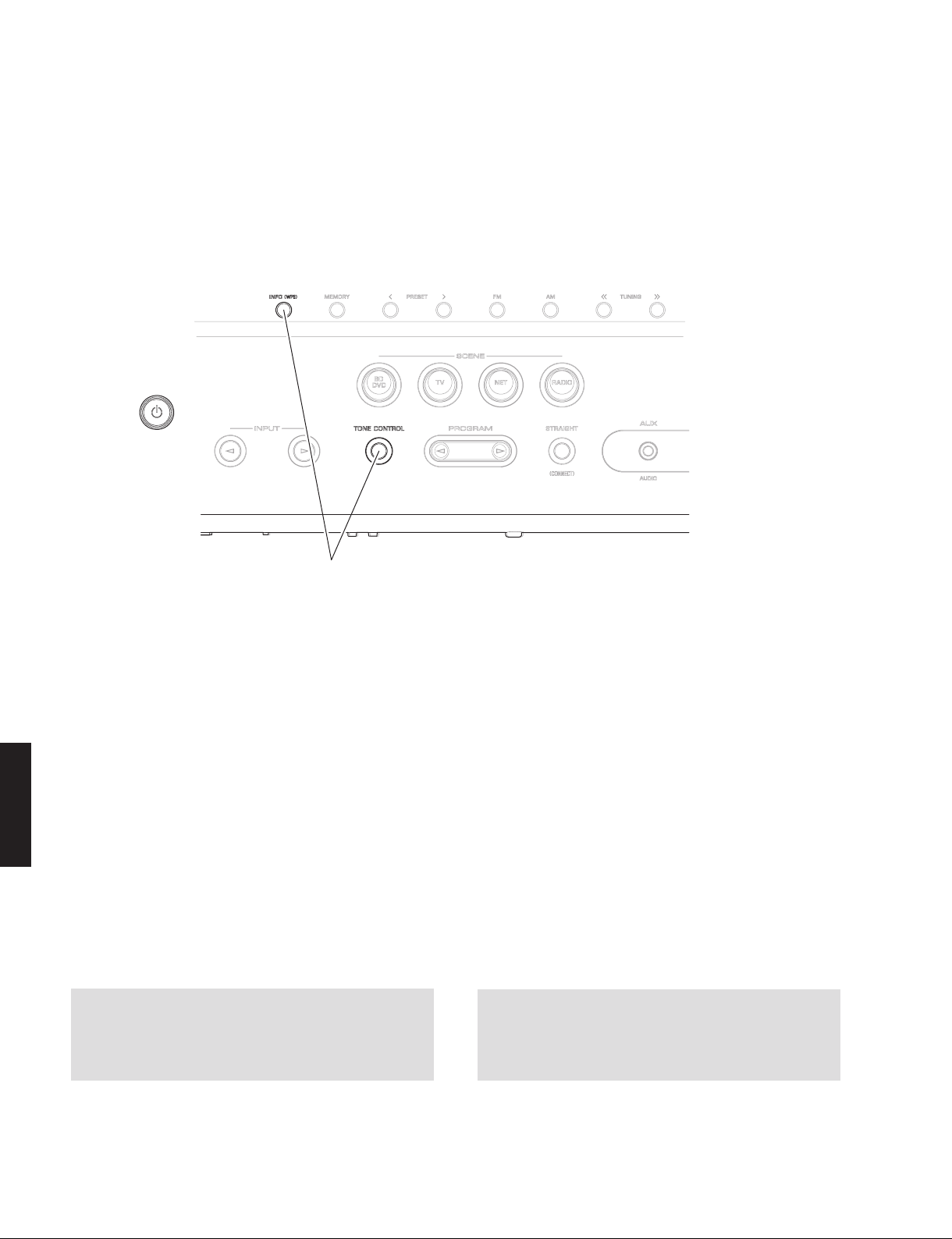
● Starting Self-Diagnostic Function
While pressing the “TONE CONTROL” and “INFO” keys,
press the “z” (Power) key to turn on the power, and
release those 2 keys.
The self-diagnostic function mode is activated.
Keys of this unit / 本機キー
(Power / 電源 )
While pressing these keys, turn on the power.
これらのキーを押しながら、電源を入れます。
● ダイアグの起動
“TONE CONTROL” と “INFO” キーを押しながら “z”(電源)
キーを押して電源を入れた後、2 つのキーを放します。
ダイアグが起動します。
● Starting Self-Diagnostic Function in
the protection cancel mode
If the protection function works and causes hindrance
to troubleshooting, cancel the protection function by
the procedure below,
selfdiagnostic function mode. (The protection functions
other than the excess current detect function will be
disabled.)
While pressing the “TONE CONTROL” and “INFO” keys,
press the “z” (Power) key to turn on the power and keep
pressing those 2 keys and “z” (Power) key for 3 seconds
RX-V579/TSR-5790
or longer.
The self-diagnostic function mode is activated with the
protection fun
In this mode, the “SLEEP” segment of the FL display
flashes to indicate that the mode is self-diagnostic
function mode with the protection functions disabled.
CAUTION!
Using this unit with the protection function disabled may
cause further damage to this unit. Take special care for
this point when using this mode.
and it will be possible to enter the
ctions disabled.
● プロテクション解除モードでの起動
プロテクションが動作することにより、故障箇所の診断
に支障をきたすような場合は、次の方法によりプロテク
ションを解除した状態でダイアグモードに入ることがで
きます。(過電流検出以外のプロテクション動作を解除す
る)
“TONE CONTROL” と “INFO” キーを押しながら “z”(電源)
キーを押して電
を 3 秒以上押し続けます。
プロテクション解除モードでダイアグが起動します。
このモードでは FL の “SLEEP” セグメントが点滅し、プロ
テクションを解除した状態でのダイアグモードであるこ
とを知らせます。
注意!
プロテクションを解除した状態でのダイアグモードは、
危険な状態でもプロテクションが作動しないため、動作
させると、本機を破壊することがあります。このモード
を使用する場合は十分注意してください。
源を入れ、2つのキーと “z”(電源)キー
30
Page 31
RX-V579/TSR-5790
● Canceling Self-Diagnostic Function
1. Before canceling self-diagnostic function, execute
setting for “S3. FACTORY PRESET” menu. (Memory
initialization inhibited or Memory initialized).
* In order to keep the user memory preserved,
be sure to select PRESET INHIBIT (Memory
initialization inhibited).
2. Press the “z” (Power) key to turn off the power.
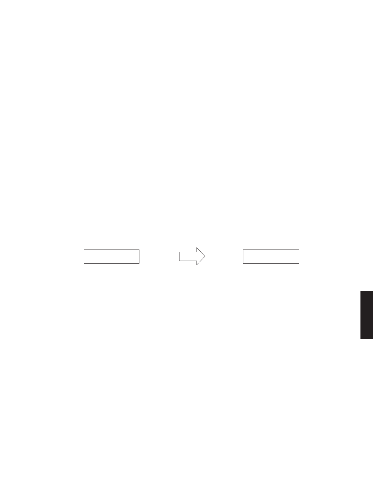
● Display provided when Self-Diagnostic
Function st
The display is as described below depending on the
situation when the power to this unit is turned off.
1. When the po wer i s turn ed off by us u al
operation:
“NO PROTECT” is displayed. Then “A1-1. DSP
MARGIN” is displayed in a few seconds.
Opening message / オープニング表示 Main menu display / メインメニュー表示
arted
● ダイアグの解除
1. ダ イ ア グ を解除する前に、“S3. FACTORY PRESET”
メニュー(メモリーの初期化禁止/またはメモリー
の初期化)の設定をします。
※ ユー ザー メ モリ ー を保 持 した い場 合 は、必 ず
PRESET INHIBIT(メモリー初期化禁止)を選択し
てください。
2. “z”(電源)キーを押して電源を切ります
。
● ダイアグ起動時の表示
本機の電源が切れたときの状況により、下記のように表
示されます。
1. 通常の操作で電源を切った場合:
“NO PROTECT” が 表 示 さ れ ま す。 数 秒 後、“A1-1.
DSP MARGIN” が表示されます。
NO PROTECT
After a few seconds / 数秒後
A1-1
DSP MARGIN
RX-V579/TSR-5790
31
Page 32

RX-V579/TSR-5790
2. When the protection function worked to turn
off the power:
The information of protection function which worked
at that time is displayed. Then “A1-1. DSP MARGIN”
is displayed in a few seconds.
Note:
At that time if you restart the self-diagnostic
function after turning off the power once, “NO
PROTECT” will be displayed. That is because
that situation is equal to “1. When the power is
turned off by us
However history of the protection function is
stored in memory as backup data. For details,
refer to “P2. PROTECTION HISTORY” menu.
2-1. When th e re i s a histo r y of prote c tion
function due to excess current.
ual operation:”.
I PROTECT
Cause:
amplifier.
Supplementary information:
amplifier is detected, the abnormal channel can be
identified by checking the current detect tr
Turning on the power without correcting the abnormality
will cause the protection function to work immediately and
the power supply will instantly be shut off.
An excessive current flowed through the power
As current of the power
ansistor.
2. プロテクションが働いて電源が切れた場合:
そのときに働いたプロテクションの情報が表示され
ます。数秒後、“A1-1. DSP MARGIN” が表示されます。
注意: このとき、一旦電源を切った後にダイアグを再
起動すると、“NO PROTECT” が表示されます。
それは、その状況が「1. 通常の操作で電源を
切った場合:」と同じだからです。
ただし、プロテクションの履歴はバックアップ
データとしてメモリーに保存されます。詳細は、
“P2. PROTECTION HISTORY” メニ ューを
してください。
2-1. 過電流によるプロテクション履歴がある場合
原因: パワーアンプに過電流が流れた。
補足: パワーアンプの電流を検出していますので、電流
検出トランジスタをチェックすれば異常チャンネ
ルが特定できます。
異常状態のまま電源を入れると、瞬時にプロテクション
が働き、すぐに電源が切れます。
参照
Notes:
• Applying the power to this unit without correcting
the abnormality can be dangerou s and cause
addi tional circuit dam age . To avoid thi s, if “I
PROTECT” protection function works 1 time, the
power will not turn on even when the “z” (Power)
key is pressed. In order to turn on the power again,
start up the self-diagnostic function.
• The output transistors in each amplifier channel
should be ch
power to this unit.
RX-V579/TSR-5790
• A m p l i f i e r cu r rent sh o u l d be monito r e d by
measuring DC voltage across the emitter resistors
for each channel.
ecked for damage before applying
注意:
• 異常状態のまま本機の電源を入れると、危険な状態
になり、さらに回路が損傷を受ける原因になります。
それを避けるために、「I PROTECT」が1回働いた場
合、それ以降 “z”(電源)キーを押しても電源が入
らなくなります。再度電源を入れる場合、ダイアグ
を起動してください。
• 本機の電源をいれる前に、各パワーアンプの出力ト
ランジスタに損傷がないかチェックしてください。
• パワーアンプの電流は、各チャンネルのエミッター
の抵抗器間 DC 電圧を測定することによりモニターし
てください。
32
Page 33
RX-V579/TSR-5790
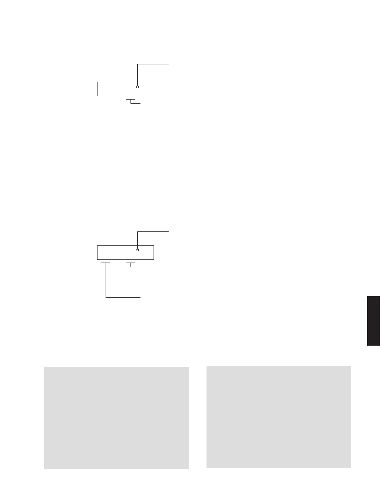
2-2. When the protection function worked due to
abnormal DC output.
H: Displayed when the voltage is HIGHER than upper limit
電圧が上限値より高い場合に表示されます
L: Displayed when the voltage is LOWER than lower limit
電圧が下限値より低い場合に表示されます
DC PRT:xxxH
xxx: A/D conversion value of voltage at the moment when the protection function worked
(Reference voltage: 3.3 V=255)
プロテクションが働いた瞬間の電圧の A/D 変換値
(基準電圧:3.3 V=255)
Cause:
Supplementary information:
worked due to a DC voltage appearing at the speaker
terminal. A cause could be a defect in the amplifier.
Turning on the power without correcting the abnormality
will cause the protection function to work in 5 seconds
and the power supply will be shut off.
DC output of the power amplifier is abnormal.
The protection function
2-3.
When the protection function worked due
to abnormal voltage in the power supply
section.
PS PRT:xxxL
xxx: A/D conversion value of voltage at the moment when the protection function worked
(Reference voltage: 3.3 V=255)
プロテクションが働いた瞬間の電圧の A/D 変換値
(基準電圧:3.3 V=255)
PS1/PS2/PS3
H: Displayed when the voltage is HIGHER than upper limit
電圧が上限値より高い場合に表示されます
L: Displayed when the voltage is LOWER than lower limit
電圧が下限値より低い場合に表示されます
2-2.
DC 出力異常によりプロテクションが働いた場合
原因: パワーアンプの DC 出力が異常。
補足: アンプの故障でスピーカー端子に直流電圧が掛か
るなどが原因で、プロテクションが働いたことを
示します。
異常状態のまま電源を入れると、5 秒後にプロテクション
が働き、電源が切れます。
2-3. 電源部の電圧異常によりプロテクションが働い
た場合
RX-V579/TSR-5790
Cause:
The voltage in the power supply section is
abnormal.
Supplementary information:
The protection function
worked due to a defect or overload in the power supply.
Turning on the power without correcting the abnormality
will cause the protection function to work in 1 seconds
and the power supply will be shut off.
Notes:
• Applying the power to this unit without correcting
the abnormality can be dangerou s and cause
additional circuit damage. To avoid this, if “PS”
an d “ DC” pro tec tio n function works 3 time s
consecutively, the power will not turn on even
when the “z” (Power) key is pressed. In order
to turn on t he p ower ag ai n, start up the selfdiagnostic function.
• The output transistors in each amplifier cha
should be checked for damage before applying
power to this unit.
• A m p l i f i e r cu r rent sh o u l d be monito r e d by
measuring DC voltage across the emitter resistors
for each channel.
nnel
原因: 電源部の電圧が異常。
補足: 電源電圧による原因で、プロテクションが働いた
ことを示します。
異常状態のまま電源を入れると
、1 秒後にプロテクション
が働き、電源が切れます。
注意:
• 異常状態のまま本機の電源を入れると、危険な状態
になり、さらに回路が損傷を受ける原因になります。
それを避けるために、「DC」、「PS」プロテクション
が連続して 3 回目働いた場合、それ以降 “z”(電源)
キーを押しても電源が入らなくなります。再度電源
を入れる場合、ダイアグを起動してください。
• 本機の電源をいれる前に、各パワーアンプの出力ト
ランジスタに損傷がないかチェックしてください。
• パワーアンプの電流は、各チャンネルのエミッター
の抵抗器間 DC 電圧を測定することによりモニターし
てください。
33
Page 34
RX-V579/TSR-5790
2-4. When the protection function worked due
to excessive heatsink/bridge diode (D2146)
temperature.
H: Displayed when the voltage is HIGHER than upper limit
電圧が上限値より高い場合に表示されます
L: Displayed when the voltage is LOWER than lower limit
電圧が下限値より低い場合に表示されます
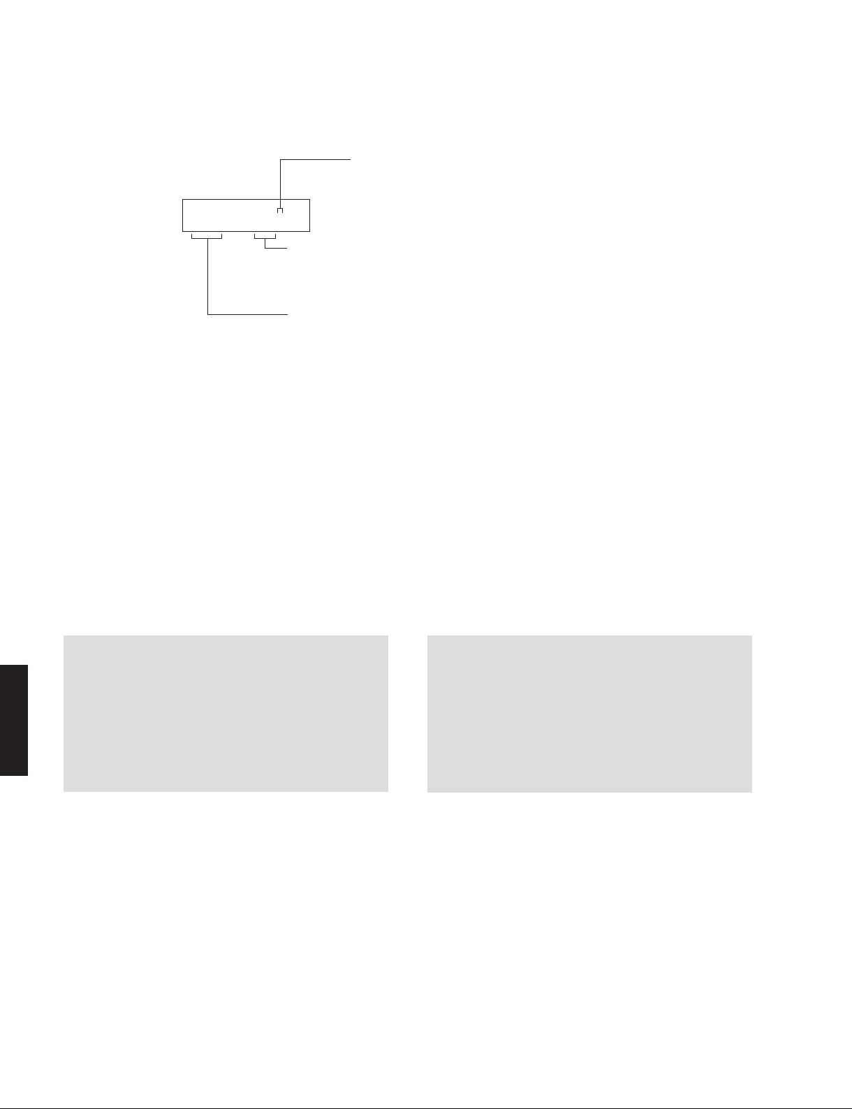
TMPxPRT:xxxL
xxx: A/D conversion value of voltage at the moment when the protection function worked
(Reference voltage: 3.3 V=255)
プロテクションが働いた瞬間の電圧の A/D 変換値
(基準電圧:3.3 V=255)
TMP1: Heatsink
TMP2: Bridge diode
Cause:
Supplementary information:
worked due to the temperature limit being exceeded.
Causes could be poor ventilation or a defect related to
the thermal sensor.
Turning on the power without correcting the abnormality
will cause the protect
and the power supply will be shut off.
The temperature of the heatsink/bridge diode
(D2146) is excessive.
The protection function
ion function to work in 1 seconds
2-4. ヒートシンク / ブリッジダイオード (D2146) の
異常温度によりプロテクションが働いた場合
原因: ヒートシンク / ブリッジダイオード
(D2146) の温
度が異常。
補足: 温度制限を越えた原因で、プロテクションが働い
たことを示します。
異常状態のまま電源を入れると、1 秒後にプロテクション
が働き、電源が切れます。
● History of protection function
When the protection function has worked, its history
is stored in memory as backup data.
Even if no abnormality is noted while servicing the
unit, an abnormality which has occurred previously
can be defined as long as the backup data has
been stored.
RX-V579/TSR-5790
For details, refer to “P2. PROTECTION HISTORY”
menu.
● プロテクションの履歴
プロテクションが働いた場合、その履歴はバック
アップデータとしてメモリーに保存されます。
修理のときに異常が認められなくても、バックアッ
プデータが残っていれば、お客様のところで起きた
異常を区別できます。
詳細は、“P2. PROTECTION HISTORY” メニ ュ ー を
参照してください。
34
Page 35
RX-V579/TSR-5790
● Operation procedure of Main menu
and Sub-menu
Each item has a main menu, each of which has sub-menu
items.
Main menu selection
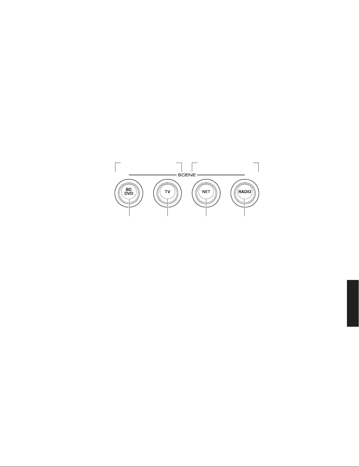
Select the main menu using “SCENE TV” (forward) and
“SCENE BD/DVD” (reverse) keys.
Sub-menu selection
Select the sub-menu using “SCENE RADIO” (forward) and
“SCENE NET” (reverse) keys.
Keys of this unit / 本機キー
Main menu selection
メインメニューの選択
● メインメニューとサブメニューの操作
ダイアグには項目別にメインメニューがあり、そのそれ
ぞれにサブメニューがあります。
メインメニューの選択
“SCENE TV”(順送り)、“SCENE BD/DVD”(逆送り)キー
で選択します。
サブメニューの選択
“SCENE RADIO”(順送り)、“SCENE NET”(逆送り)キー
で選択します。
Sub-menu selection
サブメニューの選択
Reverse
逆送り
Forward
順送り
● Functions in Self-Diagnostic Function
mode
In addition to the self-diagnostic function menu items,
functions listed below are available.
• Power ON/OFF
• Master volume
• Muting
• Input selection
* Functions related to the tuner and the set menu are not
available.
● Initial settings when Self-Diagnostic
Function started
The following initial settings are used when self-diagnostic
function is started.
When self-diagnostic function is canceled, these settings
are restored to those before starting s
function.
• Master volume: -20 dB
• Input: AV4
• Speaker setting: LARGE, Bass out to SWFR
(All channels)
• HDMI Control: Off
elf-diagnostic
Reverse
逆送り
Forward
順送り
● ダイアグ中の機能
ダイアグメニューの他に、以下の機能が動作します。
・ 電源 オン/オフ
・ マスターボリューム
・ ミュート
・ インプットセレクト
※ チューナー関連、セットメニュー関連は機能しません
● ダイアグ開始時の初期設定
ダイアグ開始時に以下のような設定になります。
ダイアグ解除時にはダイアグ開始前の状態に戻ります。
・ マスターボリューム: -20 dB
・ インプット: AV4
・ スピーカー設定: LARGE、Bass out to SWFR
(すべてのチャンネル)
・ HDMI コントロール: OFF
RX-V579/TSR-5790
。
35
Page 36
RX-V579/TSR-5790
● Details of Self-Diagnostic Function
menu
A1. DSP AUDIO
This menu is used to check audio signal route via
DSP.
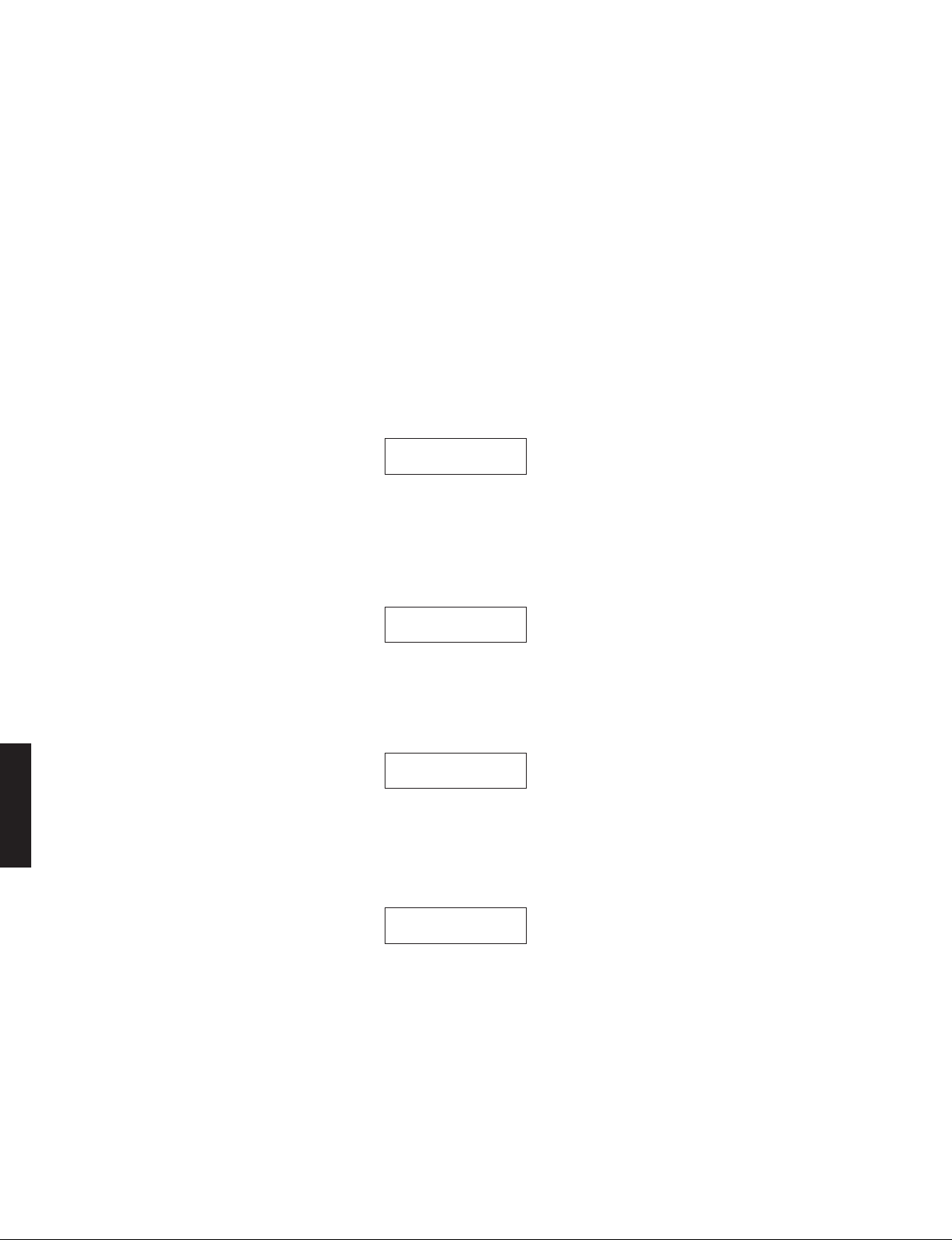
A1-1. DSP MARGIN
The audio signal is output including the head
margin via DSP.
* When input source is stereo, sign al is
assigned as below.
Fro n t L: Front L, Ce nter, Surround L,
Surround Back L
Front R: Front R, Surround R, Surround Back
R
Front L +10 dB: Subwoofer
A1-1
DSP MARGIN
A1-2. DSP NON MARGIN
The SUBWOOFE
the head margin via DSP.
The audio signal other than SUBWOOFER is
output without including the head margin via
DSP.
R signal is output including
A1-2
DSP NON MARGIN
● ダイアグメニュー詳細
A1. DSP AUDIO
DSP を経由する音声信号の経路をチェックします。
A1-1. DSP MARGIN
音声信号が DSP を経由してヘッドマージンを
含んで出力されます。
※ 2ch 信号入力時、以下のように信号が振り
分けられて出力されます。
Front L: Front L、Center、Surround L、
Surround Back L
Front R: Front R、Surround R、Surround
Back R
Front L +10 dB: Subwoofer
A1-2. DSP NON MARGIN
サブウーファーの音声信号が DSP を経由して
ヘッドマージンを含んで出力されます。
サブウーファー以外の音声信号は DSP を経由
してヘッドマージンを含まず出力されます。
A1-3. DSP FULL CENTER
A1-4. DSP FULL SURROUND
RX-V579/TSR-5790
The audio signal is output to only CENTER
channel in digital full bit without including the
head margin.
A1-3
DSP FULL C
The audio signal is output to only SURROUND
L/R channels in digital full bit without including
the head margi
n.
A1-4
DSP FULL SUR
A1-3. DSP FULL CENTER
音声信号がヘッドマージンを含まず、デジタル
フルビットで CE
されます。
A1-4. DSP FULL SURROUND
音声信号がヘッドマージンを含まず、デジタル
フルビットで SURROUND L/R チャンネルのみ
へ出力されます。
NTER チャンネルのみへ出力
36
Page 37

RX-V579/TSR-5790
A1-5. DSP FULL SURROUND BACK
The audio signal is output to only SURROUND
BACK L/R channel in digital full bit without
including the head margin.
A1-6. DSP FULL SUBWOOFER
The audio signal is output to only SUBWOOFER
channel in digital full bit without including the
head margin.
A2. DIRECT AUDIO
This menu is used to check audio signal route of
DIRECT mode.
A2-1. ANALOG DIRECT
The analog input audio signal
FRONT L and FRONT R channels in DIRECT
mode.
is output to
A1-5. DSP FULL SURROUND BACK
音声信号がヘッドマージンを含まず、デジタル
フルビットで SURROUND BACK L/R チャンネ
ルのみへ出力されます。
A1-5
DSP FULL SB
A1-6. DSP FULL SUBWOOFER
音声信号がヘッドマージンを含まず、デジタル
フルビットで SUBWOOFER チャンネルのみへ
出力されます。
A1-6
DSP FULL SW
A2. DIRECT AUDIO
DIRECT モードの音声信号の経路をチェックします。
A2-1. ANALOG DIRECT
アナ ログ入力の音声 信号が DIRECT モードで
FRONT L、FRONT R チャンネルへ出力されま
す。
A2-2. NET DIRECT
Not for service.
A2-1
ANALOG DIRECT
A2-2
Invalidity
A2-2. NET DIRECT
サービスでは使用しません。
RX-V579/TSR-5790
37
Page 38
RX-V579/TSR-5790
A3. HDMI AUDIO
This menu is used to check the route of audio signal
input to HDMI IN/OUT jack.
* Before check using “A3-2. ARC” menu, be sure to
connect a TV monitor equipped with Audio Return
Channel function to this unit in advance.
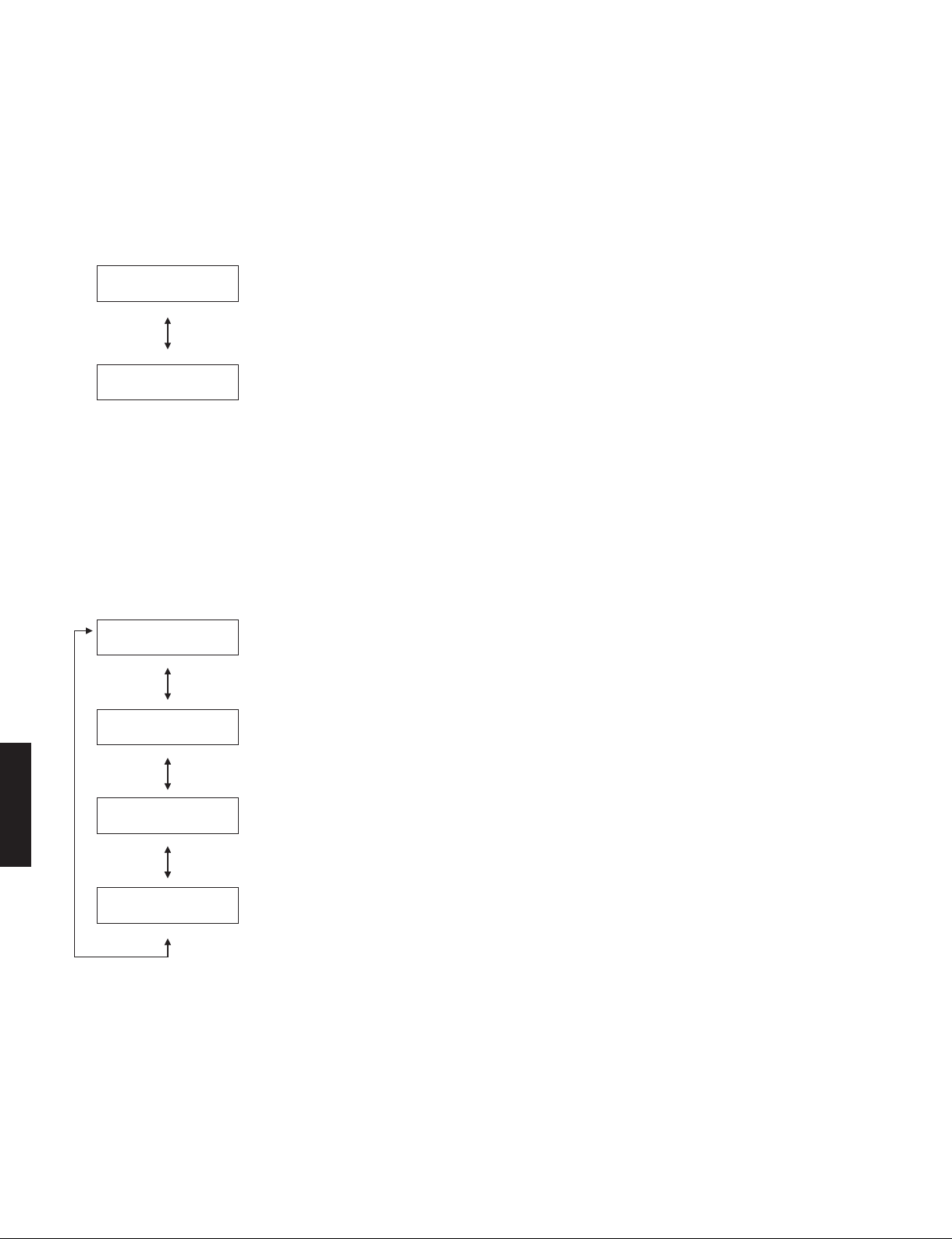
A3-1
HDMI AUTO
A3-2
ARC
A3-1. HDMI AUTO
The audio signal input to selected HDMI IN jack is output.
選択された HDMI IN 端子へ入力された音声信号が出力されます。
A3-2. ARC (Audio Return Channel function)
The audio signal input to HDMI OUT jack is output.
HDMI OUT 端子へ入力された音声信号が出力されます。
A4. SPEAKERS SET
This menu is used to check the speaker output.
A3. HDMI AUDIO
HDMI IN/OUT 端子へ 入 力 さ れた音声信号の経路を
チェックします。
※ “A3-2. ARC” メニューでのチェックの前に、あら
かじめ必ず Audio Return Channel 機能に
いるテレビを接続してください。
A4. SPEAKERS SET
スピーカー出力をチェックします。
対応して
A4-1
FULL MUTE
A4-2
BI-AMP
A4-3
AC_B:Hi
RX-V579/TSR-5790
A4-4
AC_B:Lo
A4-1. FULL MUTE
The audio signals are muted at all channels.
音声信号がすべてのチャンネルでミュートされます。
A4-2. BI-AMP
The FRONT L/R signal is distributed to SURROUND BACK L/R terminals.
FRONT L/R の音声信号が SURROUND BACK L/R 端子へ振り分けられて出力されます。
A4-3. AC B HIGH
Not for service.
サービスでは使用しません。
A4-4. AC B LOW
Not for service.
サービスでは使用しません。
38
Page 39
RX-V579/TSR-5790
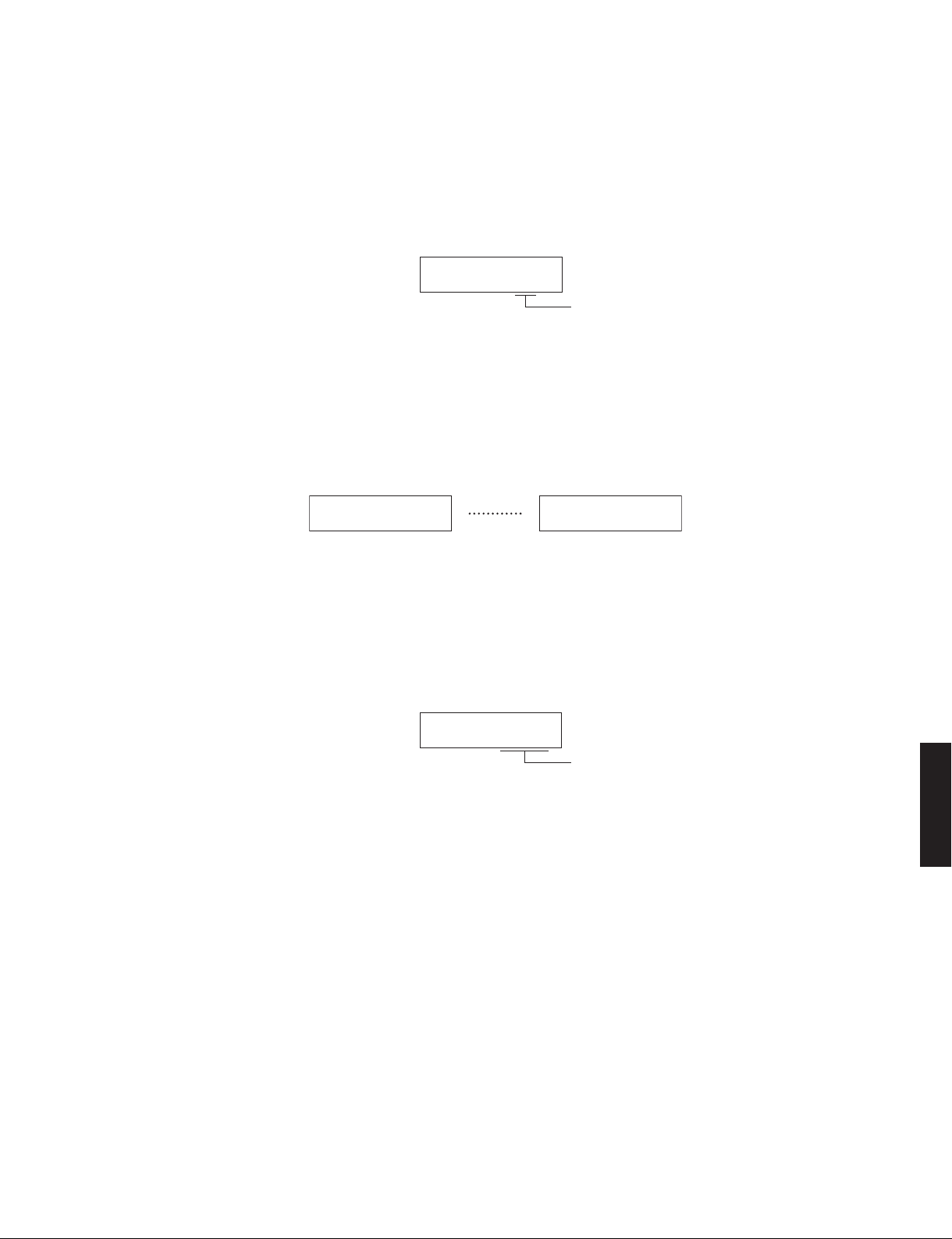
A5. MIC CHECK
A5-1. MIC ROUTE CHECK
The audio signal input to the YPAO MIC jack is
output to FRONT L channel via A/D-D/A.
A6. INVALID ITEM
Not for service.
A6-1
Invalidity
A5. MIC CHECK
A5-1. MIC ROUTE CHECK
YPAO マイク端子へ入力された音声信号が A/D
− D/A 経由で FRONT L チャンネルへ出力され
ます。
A5-1
MIC ROUTE ON
ON: Connected / 接続されている
OFF: Unconnected / 接続されていない
A6. INVALID ITEM
サービスでは使用しません。
A6-3
Invalidity
A7. DIR PLL (Phase Lock Loop)
This menu is used to check the route of digital audio
signal input to AV1, AV2, AV3 jack.
A7. DIR PLL (Phase Lock Loop)
A7-1
DIR PLL:---
AV1、AV2、AV3 端子へ入力されたデジタル音声信号
の経路をチェックします。
RX-V579/TSR-5790
Lock: Lock / 同期
Unlock: Unlock or unconnected /
非同期または接続されていない
---: Inputted to the non-target INPUT/
非対象 INPUT へ入力されている
39
Page 40
RX-V579/TSR-5790
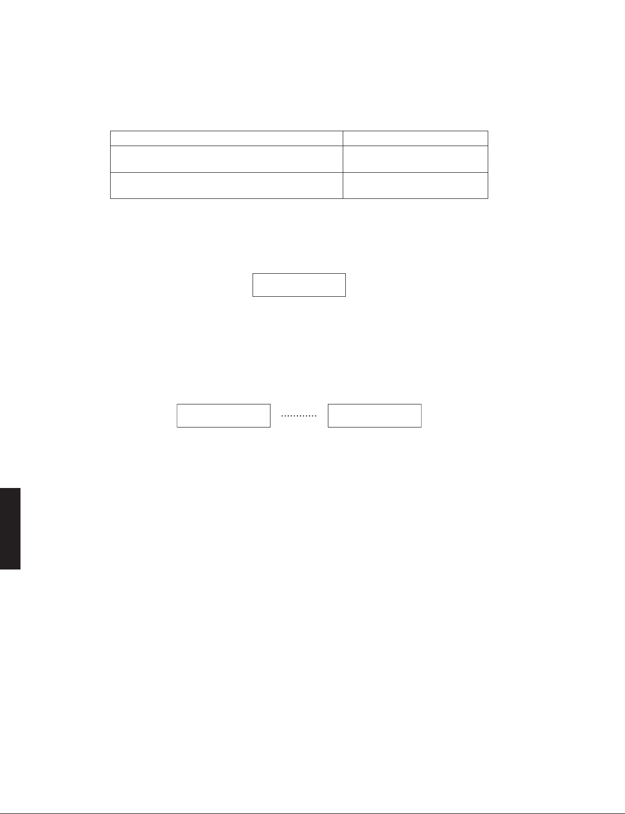
A8. MANUAL TEST
The test noise generated by built-in noise generator
in DSP is output to the channels specified by the submenu.
for SUBWOOFER / SUBWOOFER 用
for other than SUBWOOFER / SUBWOOFER 以外
A8-1. TEST ALL
The test noise is output to all channels.
H1. INVALID ITEM
Not for service.
A8. MANUAL TEST
DSP に内蔵されたノイズジェネレータによって生成
されたテストノイズが、サブメニューで指定したチャ
ンネルへ出力されます。
Test noise / テストノイズ
30 Hz to 80 Hz
pink noise / ピンクノイズ
500 Hz to 2 kHz
pink noise / ピンクノイズ
A8-1. TEST ALL
テストノイズが全てのチャンネルへ出力されま
す。
A8-1
TEST ALL
H1. INVALID ITEM
サービスでは使用しません。
RX-V579/TSR-5790
H1-1
Invalidity
H1-2
Invalidity
40
Page 41
RX-V579/TSR-5790
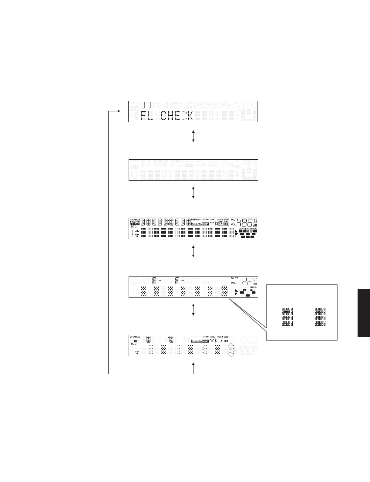
D1. FL CHECK
This menu is usedt to check operation of the FL
display.
D1-1. INITIAL DISPLAY / 初期表示
D1-2. ALL SEGMENT OFF / 全セグメント消灯
D1-3. ALL SEGMENT ON / 全セグメント点灯
D1. FL CHECK
FL 表示の動作をチェックします。
FL display / FL 表示
D1-4. CHECK PATTERN 1 / チェックパターン 1
D1-5. CHECK PATTERN 2 / チェックパターン 2
Segment conditions of the FL tube is checked by
turning ON and OFF all segments.
Next, a short between segments next to each other
is checked by turning ON and OFF all segments
alternately (in lattice).
(In the above example, the segments in the second
row from the top are shorted.)
FPL FPR
SL SW
SR
SBSBL SBR
* After check, change to next menu at once.
確認後、すみやかに次のサブメニューを選択してください。
FPL FPR
SL SW
SBSBL SBR
Example / 例
SR
Lighting on segments in lattice.
セグメント格子状点灯
Normal
正常
FPL FPR
SL SW
SR
SBSBL SBR
Short
ショート
全セグメント消灯・全セグメント点灯により FL 管
セグメントの不良を確認します。
次に、全セグメントを交互(格子状)に点灯/消灯
することで、隣り合うセグメントのショートをチェッ
クします。
(上記の例は、上から 2 列目のセグメントがショート
しています。)
RX-V579/TSR-5790
の
41
Page 42
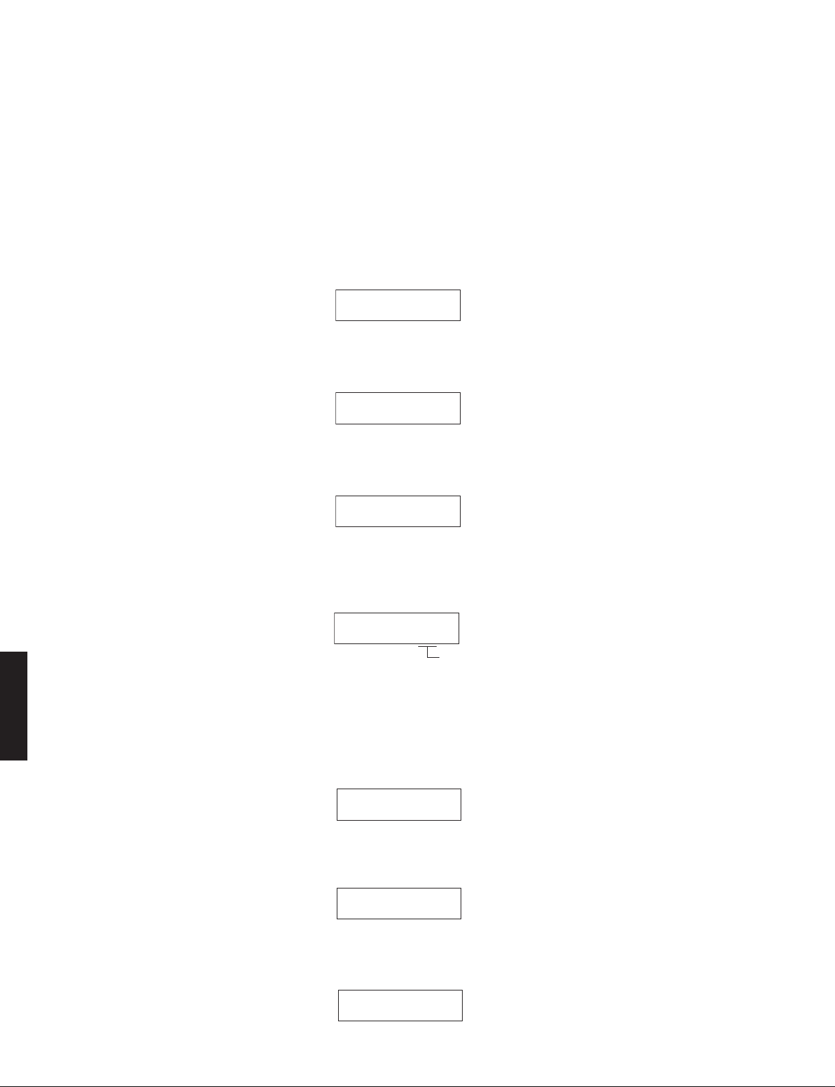
RX-V579/TSR-5790
U1. USB
This menu is used to check the audio signal route
from USB storage device.
U1-1. USB FRONT 1 TRACK
The 1st music file stored in the USB storage
de v ice conn e cted to th e US B j ack is
reproduced.
* Copy 2 or more music files from PC to the
root folder of the USB storage device in
advance.
U1-2. USB BOOT
Not for service.
U1-3. INVALID ITEM
Not for service.
U1. USB
U1-1
USB_F 1 TRACK
U1-2
USB BOOT:--
USB フラッ シ ュメモリーか ら の音声信号の経 路を
チェックします。
U1-1. USB FRONT 1 TRACK
USB 端子に接続された USB フラッシュメモ
リーに保存された音楽ファイルの 1 曲目が再生
されます。
※ あらかじめPCから USB フラッシュメモリー
のルートフォルダに音楽ファイルを 2 曲以
上コピーしてください。
U1-2. USB BOOT
サービスでは使用しません。
U1-3. INVALID ITEM
サービスでは使用し
ません。
U1-4. USB AUDIO
U2. USB COMPLIANCE TEST
Not for service.
RX-V579/TSR-5790
U2-1. TEST SEO NAK
U2-2. TEST J
This menu is used to check if th
from USB storage device is output to DSP.
Not for service.
Not for service.
e audio signal
U1-3
Invalidity
U1-4. USB AUDIO
USB フラッシュメモリーから音声信号が DSP
に来ているかチェックします。
U1-4
USB AUDIO:OK
OK: Normal / 正常
NG: Abnormal / 異常
--: Checking / チェック中
U2. USB COMPLIANCE TEST
サービスでは使用しません。
U2-1. TEST SEO NAK
サービスでは使用しません。
U2-1
TEST SEO NAK
U2-2. TEST J
サービスでは使用しません。
U2-2
TEST J
42
U2-3. TEST K
Not for service.
U2-3. TEST K
サービスでは使用しません。
U2-3
TEST K
Page 43
RX-V579/TSR-5790
U2-4. TEST PACKET
Not for service.
N1. NETWORK
This menu is used to check functions related to
NETWORK.
Connect between LAN port of broadband router and
NETWORK jack of this unit with a network cable.
* When the network condition varies while sub-menu
is displayed (e.g., the network is deactivated
once), the correct result will not be displayed.
In that case, once turn off the power to this unit,
then s
tart up the self-diagnostic function again and
select this menu.
N1-1. IP ADDRESS CHECK
This menu is used to check that IP address
can be obtained.
U2-4. TEST PACKET
サービスでは使用しません。
U2-4
TEST PACKET
N1. NETWORK
ネットワークに関連する機能をチェックします。
ブ ロ ードバ ン ドル ー ター の LAN ポ ートと 本 機の
NETWORK 端子をネットワークケーブルで接続しま
す。
* サブメニュー表示中にネットワークの状態が変わ
ると(たとえばネットワークが一時切れるなど)
正しい結果が表示されません。
その場合、一度本機の電源を切り、ダイアグを再
起動して本メニューを選択します。
N1-1. IP ADDRESS CHECK
IP アドレスが取得されていることをチェックし
ます。
N1-1
IP AD CHK:OK
OK: Connected (IP address obtained)
接続(IP アドレス取得完了)
NG: No traffic / Disconnected
通信不能/接続が切れている
N1-2. MAC ADDRESS CHECK
This menu is used to check that MAC address
is written.
N1-3. LINE NOISE 100 MDI
Not for service.
N1-4. LINE NOISE 100 MDIX
Not for service.
N1-5. LINE NOISE 10 MDI
Not for service.
N1-2
MAC AD CHK:OK
N1-3
LN MDI 100
N1-4
LN MDIX 100
N1-2. MAC ADDRESS CHECK
MAC ア ドレ ス が 書 き 込 ま れ てい るこ と を
チェックします。
RX-V579/TSR-5790
OK: Normal / 正常
NG: Unwritten / 書き込まれていない
N1-3. LINE NOISE 100 MDI
サービスでは使用しません。
N1-4. LINE NOISE 100 MDIX
サービスでは使用しません。
N1-5 LINE NOISE 10 MDI
サービスでは使用しません。
N1-5
LN MDI 10
43
Page 44
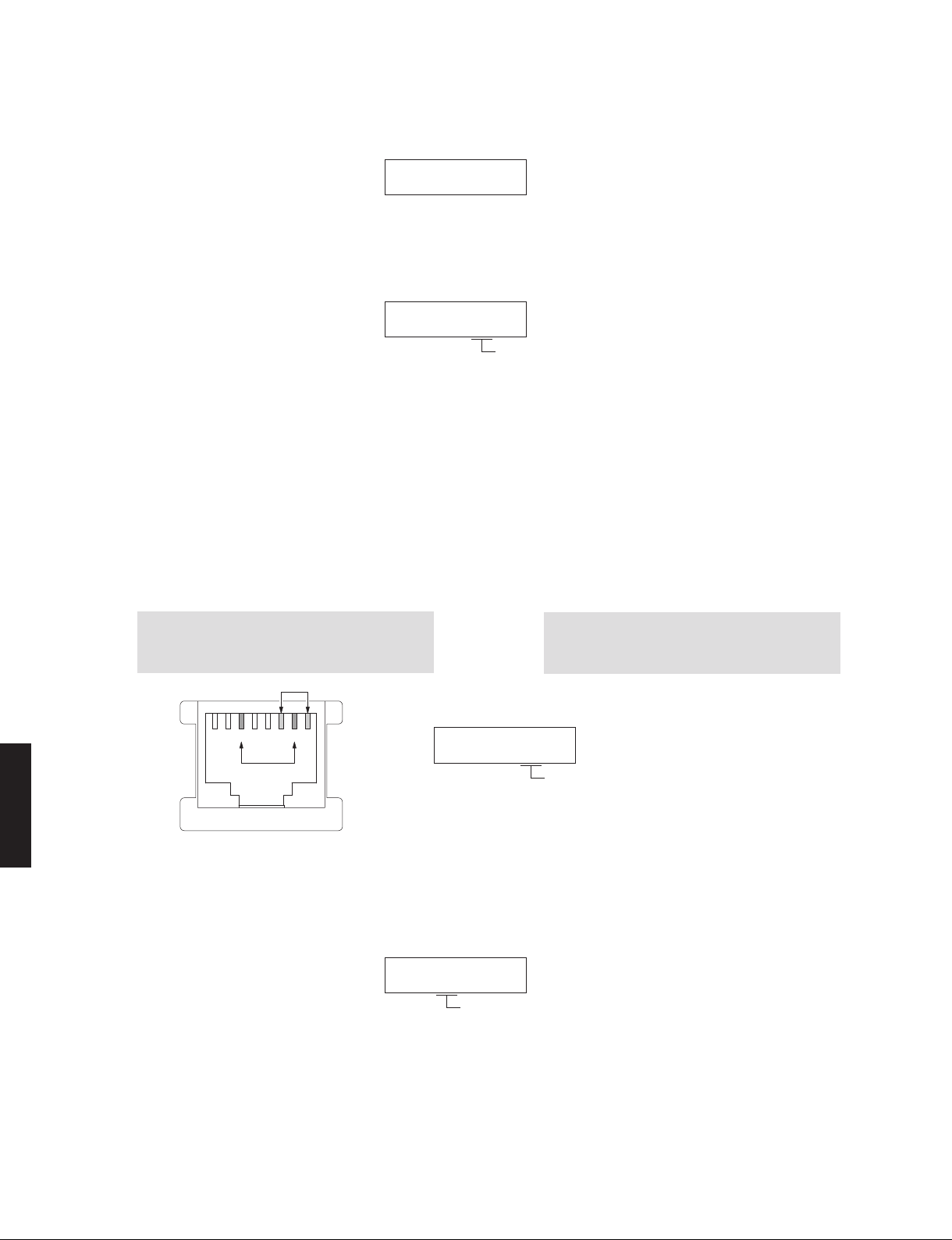
RX-V579/TSR-5790
N1-6. LINE NOISE 10 MDIX
Not for service.
N1-7. LINK CHECK
This menu is used to check that the broadband
router is connected correctly.
N1-8. EXT TEST
Transmission/reception of the NETWORK port
is checked.
With the power turned off, short the pins of the
NETWORK jack as shown in the figure below.
Start up the self-diagnostic function and select
this menu.
Transmission/reception test is executed and its
re
sult is displayed.
N1-6. LINE NOISE 10 MDIX
サービスでは使用しません。
N1-6
LN MDIX 10
N1-7. LINK CHECK
ブロードバンドルーターが正しく接続されてい
ることをチェックします。
N1-7
LINK CHK:OK
OK: Connected / 接続
NG: No traffic / Disconnected
通信不能/接続が切れている
N1-8. EXT TEST
NETWORK ポートの送受信テストを行います。
電源を切った状態で、下図のように NETWORK
端子のピンをショートさせます。
ダイアグを起動して本メニューを選択します。
送受信テストを行い、その結果が表示されます。
RX-V579/TSR-5790
N1-10. PING
Note:
Be sure to return the shorted pins to their
original condition after executing this test.
12345678
NETWORK jack
Transmit the PING command.
N1-10
PING:OK
注意:
検査後、ショートしたピンを必ず元の状態に
戻してください。
N1-8
EXT TEST:OK
OK: Normal / 正常
NG: Abnormal / 異常
--: Checking / チェック中
N1-10. PING
PING コマンドを送信します。
OK: Normal / 正常
NG: Abnormal / 異常
--: Checking / チェック中
44
Page 45
RX-V579/TSR-5790
N2. WIFI
Not for service.
N2-1–N2-10. WIFI ON JIG01
Not for service.
N2-11. WIFI OFF
Not for service.
N2-12. WIFI MAC ADDRESS
Not for service.
N2-13. WIFI RF TEST
Not for service.
N2-1
WIFI ON JIG01
N2-11
WIFI OFF
N2-12
6CECEB 113D8A
・・・・・・・・・・・
N2. WIFI
サービスでは使用しません。
N2-1–N2-10. WIFI ON JIG01
サービスでは使
N2-10
WIFI ON JIG10
N2-11. WIFI OFF
サービスでは使用しません。
N2-12. WIFI MAC ADDRESS
サービスでは使用しません。
N2-13. WIFI RF TEST
サービスでは使用しません。
用しません。
N3. BLUETOOTH
Not for service.
N3-1. BLUETOOTH VERSION
Not for service.
N3-2. BLUETOOTH ADDRESS
Not for service.
N3-3. BLUETOOTH PLAYBACK
Not for service.
N2-13
WIFI RF TEST
N3. BLUETOOTH
N3-1
BT VERSION
N3-2
BT Address
N3-3
PLAYBACK
サービスでは使用しません。
N3-1. BLUETOOTH VERSION
サービスでは使用しません。
N3-2. BLUETOOTH ADDRESS
サービスでは使用しません。
N3-3. BLUETOOTH PLAYBACK
サービスでは使用しません。
RX-V579/TSR-5790
N3-4 ~ N3-10
Not for service.
N3-4
T.B.D
N3-4 ~ N3-10
サービスでは使用しません。
N3-10
T.B.D
45
Page 46
RX-V579/TSR-5790
N4. NET AUDIO
N4-1. LOOPBACK 0 TEST
Signal route that selected in the sub-menu
loops back among DSP (IC41) → DAC (IC62)
→ Volume IC (IC203) → DIR (ADC) (IC61) →
Network Module → DSP (IC41), and then the
analysis result is displayed.
NCPU_SD0 signal route is checked.
N4-2. LOOPBACK 1 TEST
NCPU_SD1 signal route is checked.
N4-3. LOOPBACK 2 TEST
NCPU_SD2 signal route is checked.
N4. NET AUDIO
N4-1. LOOPBACK 0 TEST
N4-1
LOOPBK0:OKO---
N4-2. LOOPBACK 1 TEST
N4-2
LOOPBK1:OK-O--
N4-3. LOOPBACK 2 TEST
N4-3
LOOPBK2:OK--O-
DSP (IC41) → DAC (IC62) →Volume IC (IC203)
→ DIR (ADC) (IC61) → ネットワークモジュー
ル → DSP (IC41) 間をサブメニューで選択され
た信号経路でループバックし、その解析結果が
表示されます。
NCPU_SD0 の信号経路をチェックします。
O: Signal exists / 信号あり
-: No signal / 信号なし
OK: Normal / 正常
NG: Abnormal / 異常
--: Checking / チェック中
NCPU_SD1 の信号経路をチェックします。
NCPU_SD2 の信号経路をチェックします。
N4-4. LOOPBACK 3 TEST
N4-5. NET AUDIO PLAYBACK 0 TEST
RX-V579/TSR-5790
N4-6. NET AUDIO PLAYBACK 1 TEST
N4-7. NET AUDIO PLAYBACK 2 TEST
NCPU_SD3
signal route is checked.
N4-4
LOOPBK3:OK---O
The sine wave generated by Network Module
is output to selected signal line in sub-menu.
DSP (IC41) receives the output signal, and
then the analysis result is displayed.
NCPU_SD0 signal route is checked.
N4-5
N APB0: OKO---
NCPU_SD1 signal route is checked.
N4-6
N APB1: OK-O--
NCPU_SD2 signal route is checked.
N4-7
N APB2: OK--O-
N4-4. LOOPBACK 3 TEST
NCPU_SD3 の信号経路
N4-5. NET AUDIO PLAYBACK 0 TEST
ネットワークモジュールで生成された正弦波をサ
ブメニューで選択された信号経路に出力します。
その信号を DSP (IC41) で受け取り、解析結果
が表示されます。
NCPU_SD0 の信号経路をチェックします。
N4-6. NET AUDIO PLAYBACK 1 TEST
NCPU_SD1 の信号経路をチェックします。
N4-7. NET AUDIO PLAYBACK 2 TEST
NCPU_SD2 の信号経路をチェックします。
をチェックします。
46
N4-8. NET AUDI
NCPU_SD3 signal route is checked.
N4-9. LOOPBACK ZONE DAC TEST
Not for service.
O PLAYBACK 3 TEST
N4-8. NET AUDIO PLAYBACK 3 TEST
NCPU_SD3 の信号経路をチェックします。
N4-8
N APB3: OK---O
N4-9. LOOPBACK ZONE DAC TEST
サービスでは使用しません。
N4-9
N APB TO Z2:--
Page 47

RX-V579/TSR-5790
N5. SPI LOOPBACK
N5-1. SPI LOOPBACK TEST
This menu is used to check the SPI connection
between NET Micropro cessor and MAIN
Microprocessor.
C1. ACCESS CHECK
This menu is used to check the communication and
bus line connection between devices on DIGITAL
P.C.B.
C1-1. ALL
The total detection result of sub-menus from
C1-2 to C1-8 is displayed.
N5-1
SPI:--
C1-1
All:OK
N5. SPI LOOPBACK
N5-1. SPI LOOPBACK TEST
NET マイコ ンと MAIN マ イコンの SPI 接続を
チェックします。
C1. ACCESS CHECK
DIGITAL P.C.B. 上の各デバイス間の通信とバスライン
接続をチェックします。
C1-1. ALL
サブメニュー C1-2 〜 C1-8 の総
表示されます。
OK: No error detected / 不良検出なし
NG: An error is detected / 不良検出あり
--: Checking / チェック中
合判定結果が
C1-2. MCPU OSD
Reading/writing function of Microprocessor
(IC21) to
C1-3. OSD HDMI
Reading/writing function of HDMI IC (IC1) to
OSD FLASH ROM (IC2) are checked.
C1-4. VIDEO I/F
Commun icat ion and bus line connection
between microprocessor (IC21) and Video
Selector (IC502) are checked.
OSD FLASH ROM (IC2) are checked.
C1-2
MCPU OSD:OK
C1-3
OSD HDMI:OK
C1-4
VIDEO I/F:OK
C1-2. MCPU OSD
マイコン(IC21)と OSD FLASH ROM(IC2)
の読み出し/書き込みをチェックします。
OK: No error detected / 不良検出なし
NG: An error is detected / 不良検出あり
C1-3. OSD HDMI
HDMI IC(IC1)と OSD FLASH ROM(IC2)の
読み出し/書き込みをチェックします。
OK: No error detected / 不良検出なし
NG: An error is detected / 不良検出あり
C1-4. VIDEO I/F
マ イ コ ン(IC21) と Video Selector(IC502)
間の通信とバスライン接続をチェックします。
OK: No error detected / 不良検出なし
NG: An error is detected / 不良検出あり
--: Checking / チェック中
RX-V579/TSR-5790
47
Page 48

RX-V579/TSR-5790
C1-5. DIR BUS
Commun icat ion and bus line connection
between microprocessor (IC21) and DIR (IC61)
are checked.
C1-6. DSP BUS
Commun icat ion and bus line connection
between microprocessor (IC21) and DSP
(IC41) are checked.
C1-7. EEPROM
EEPROM (IC22)'s reading is checked.
C1-5
DIR BUS:OK
C1-6
DSP BUS:OK
C1-5. DIR BUS
マイコン(IC21)
バスライン接続をチェックします。
OK: No error detected / 不良検出なし
NG: An error is detected / 不良検出あり
--: Checking / チェック中
C1-6. DSP BUS
マイ コン(IC21)と DSP(IC41)間の通信と
バスライン接続をチェックします。
OK: No error detected / 不良検出なし
NG: An error is detected / 不良検出あり
--: Checking / チェック中
C1-7. EEPROM
EEPROM(IC22)の読み出しをチェックします。
と DIR(IC61) 間 の 通 信 と
C1-8. TUNER
RX-V579/TSR-5790
C1-9. BT
C1-7
EEPROM:OK
The AM/FM TUNER I2C (Inter integrated
circuit) bus line connection is checked.1
C1-8
TUNER:OK
Not for service.
C1-9
Invalidity
OK: No error detected / 不良検出なし
NG: An error is detected / 不良検出あり
--: Checking / チェック中
C1-8. TUNER
AM/FM TUNER の I2C(Inter integrated circuit)
バスライン接続をチェックします。
OK: No error detected / 不良検出なし
NG: An error is detected / 不良検出あり
--: Checking / チェック中
C1-9. BT
サービスでは使用しません。
48
Page 49

RX-V579/TSR-5790
C2. HDMI INFORMATION
This menu is used to display information about HDMI.
C2-1. HDMI MODEL NAME
The mo d e l na m e wr i t t e n to HDMI I C is
displayed.
C2-2. HDMI PRODUCT ID
The product ID written to this unit is displayed.
C3. NET CPU CHECK
This menu is used to check the communication and
bus line connection between devices related to
network.
C2. HDMI INFORMATION
HDMI に関する情報が表示されます。
C2-1. HDMI MODEL NAME
HDMI IC に書き込まれているモデル名が表示さ
れます。
C2-1
HMN:RX-V579
RX-V579
TSR-5790
C2-2. HDMI PRODUCT ID
本機に書き込まれているプロダクト ID が表示
されます。
C2-2
HID:31B0
C3. NET CPU CHECK
ネットワークに関連する各デバイス間の通信とバス
ラインの接続をチェックします。
C3-1. ALL
The total detection result of sub-menus from
C3-3 to C3-8 is
displayed.
C3-1
ALL:OK
C3-2. INVALID ITEM
Not for service.
C3-3. PHY (Ethernet PHYceiver) TEST
Not for service.
C3-3
PHY TEST:OK
OK: No error detected / 不良検出なし
NG: An error is detected / 不良検出あり
--: Checking / チェック中
C3-2
INVALID ITEM
OK: No error detected / 不良検出なし
NG: An error is detected / 不良検出あり
--: Checking / チェック中
C3-1. ALL
サブメニュー C3-3 〜 C3-8 の総合判定結果が
表示されます。
C3-2. INVALID ITEM
サービスでは使用しません。
C3-3. PHY (Ethernet PHYceiver) TEST
サービスでは使用し
ません。
RX-V579/TSR-5790
49
Page 50

RX-V579/TSR-5790
C3-4. APL (Apple) ID CHECK
Apple authentication IC (IC954) device ID is
checked.
C3-5. CLOCK GENERATOR CHECK
Acc ess o f Clock gener ator(S i535IC ) is
checked.
C3-6. PMIC CHECK
Access of power supply (PMIC) is checked.
C3-4
APL ID:OK
C3-5
CLK GEN:OK
C3-6
PMIC:OK
C3-4. APL (Apple) ID CHECK
Apple 認証 IC(IC954)のデバイス ID をチェッ
クします。
OK: No error detected / 不良検出なし
NG: An error is detected / 不良検出あり
--: Checking / チェック中
C
3-5. CLOCK GENERATOR CHECK
Clock generator(Si535IC)のアクセスをチェッ
クします。
OK: No error detected / 不良検出なし
NG: An error is detected / 不良検出あり
C3-6. PMIC CHECK
電源 IC(PMIC)のアクセスをチェックします。
OK: No error detected / 不良検出なし
NG: An error is detected / 不良検出あり
C3-7. WIRELESS MODULE CHECK
RX-V579/TSR-5790
C3-8. NET EEPROM CHECK
Access of wireless module is checked.
EEPROM is checked and the result is
displayed.
C3-7. WIRELESS MODULE CHECK
ワイヤレスモジュールのアクセスをチェックし
ます。
C3-7
WL MOD:OK
OK: No error detected / 不良検出なし
NG: An error is detected / 不良検出あり
C3-8. NET EEPROM CHECK
EEPROM チェックを行い結果を表示します。
C3-8
NET EEPROM:OK
OK: No error detected / 不良検出なし
NG: An error is detected / 不良検出あり
--: Checking / チェック中
50
Page 51
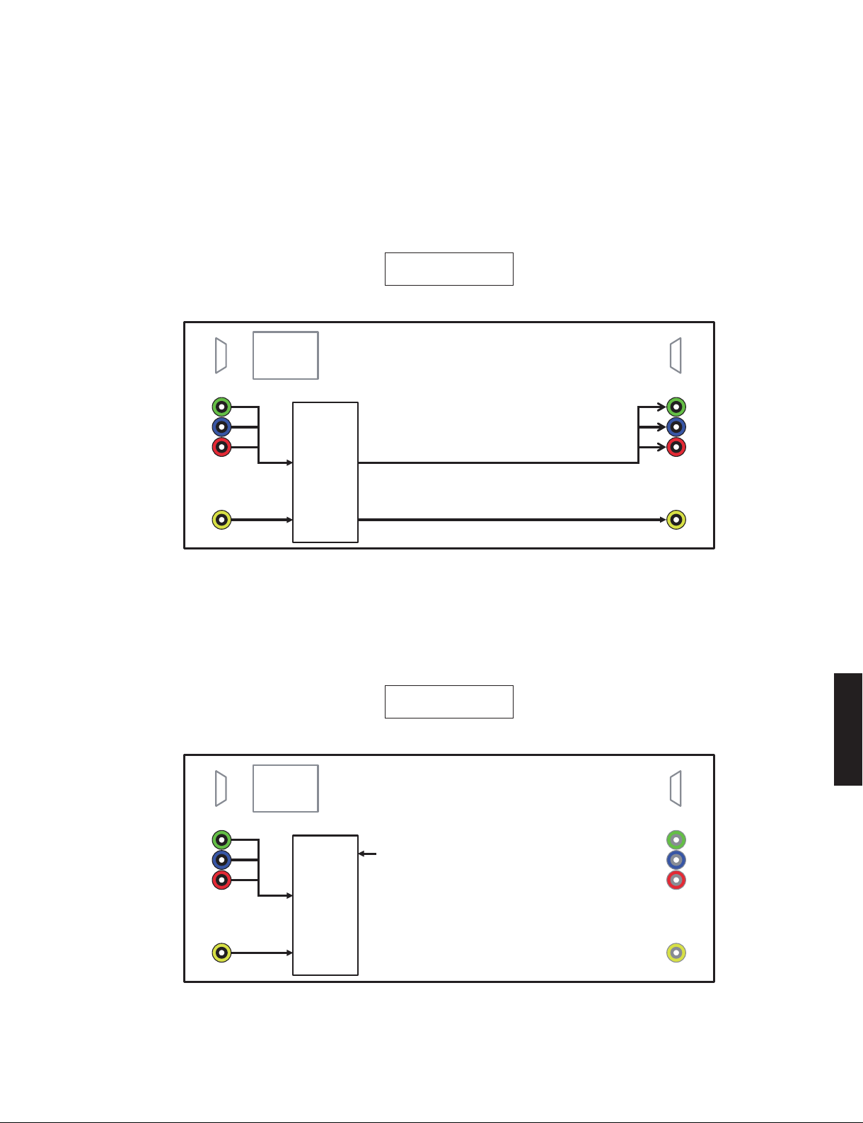
RX-V579/TSR-5790
V1. ANALOG VIDEO CHECK
This menu is used to check the analog video signal
route.
V1-1. ANALOG BYPASS
The video signal is converted and output as
shown below.
ANALOG BYPASS
HDMI IN
Component In
DIGITAL
IC1
HDMI Receiver/
Transmitter
OPERATION
IC502
Video
Selector
V1. ANALOG VIDEO CHECK
アナログ映像信号の経路をチェックします。
V1-1. ANALOG BYPASS
映像信号が以下のように変換され、出力されま
す。
V1-1
ANALOG BYPASS
HDMI OUT
Component Out
Composite In
V1-2. MUTE CHECK
The video signal is muted.
MUTE CHECK
HDMI IN
Component In
DIGITAL
IC1
HDMI Receiver/
Transmitter
OPERATION
IC502
Video
Selector
Composite Out
V1-2. MUTE CHECK
映像信号がミュートされます。
RX-V579/TSR-5790
V1-2
MUTE CHECK
HDMI OUT
Component Out
MUTE
Composite In
Composite Out
51
Page 52
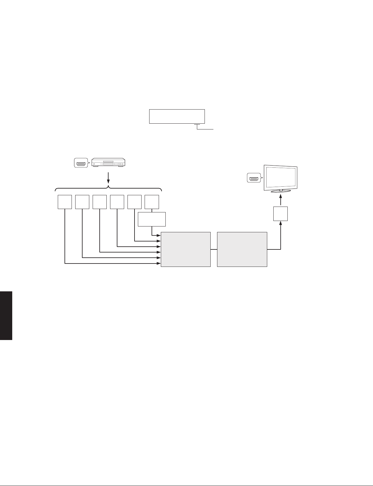
RX-V579/TSR-5790
V2. DIGITAL VIDEO CHECK
This menu is used to check the digital video signal
route.
V2-1. HDMI REPEAT
The video/audio signals input to HDMI IN jack
are output to HDMI OUT jack.
HDMI output
HDMI
BD/DVD player
CB6
HDMI
IN1
CB5
HDMI
IN2
CB4
HDMI
IN3
CB3
HDMI
IN4
CB2
HDMI
IN5
HDCP Receiver
Sil9679CNUC
V2. DIGITAL VIDEO CHECK
V2-1
HDMI REPEAT **
CB1
HDMI
IN6
IC901
デジタル映像信号の経路をチェックします。
V2-1. HDMI REPEAT
HDMI IN 端子へ入力された映像信号と音声信号
が HDMI OUT 端子へ出力されます。
The Deep Color video signals is input, “30” bit or
“36” bit is displayed.
Deep Color 映像信号を入力すると、“30” bit ま た
は “36” bit が表示
されます。
HDMI
TV
CB7
HDMI
OUT
RX-V579/TSR-5790
IC1
HDMI Receiver/Transmitter
SII9573CTUC
IC904
HDCP Receiver
Sil9678CNJC
52
Page 53
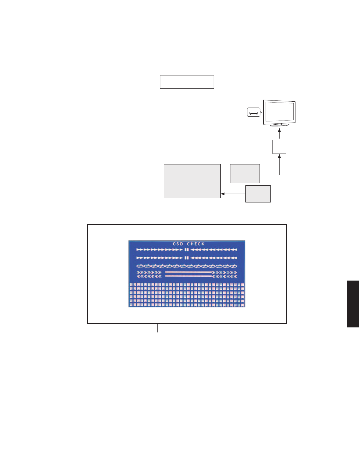
RX-V579/TSR-5790
V2-2. OSD (On-Screen Display) VIDEO OUT
The “OSD CHECK” screen is output to HDMI
OUT jack.
TV screen display /
V2-2
OSD-VIDEO OUT
IC1
HDMI Receiver/Transmitter
SII9573CTUC
TV 画面表示
V2-2. OSD (On-Screen Display) VIDEO OUT
“OSD CHECK” 画 面 が HDMI OUT 端子 へ 出 力
されます。
TV
HDMI
CB7
HDMI
OUT
IC904
HDCP Receiver
Sil9678CNJC
IC2
FLASH ROM
(OSD data)
OSD CHECK screen
OSD CHECK 画面
RX-V579/TSR-5790
53
Page 54
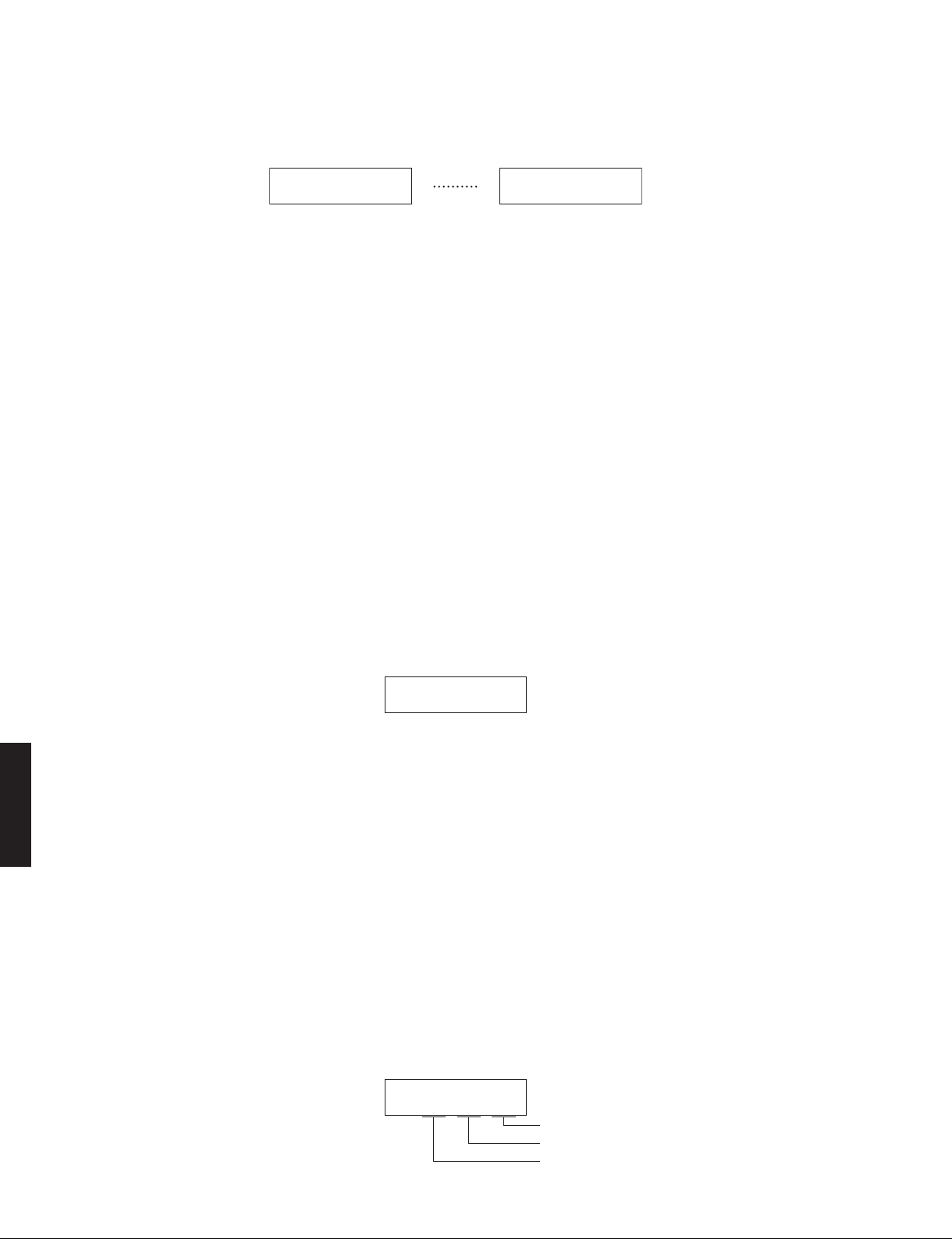
RX-V579/TSR-5790
R1. INVALID ITEM
Not for service.
R1-1
Invalidity
P1. AD DATA CHECK
This menu is used to display the A/D conversion
value of the microprocessor which detects panel keys
and protection functions by using the sub-menu.
When “P1-8. KEY1/KEY2” sub-menu is selected, keys
become inoperable due to detection of the values
of all keys. However, it is possible to advance to the
next menu by turning the VOLUME knob.
* Numeric va
only.
P1-1. DC
Power amplifier DC (DC voltage) output is
detected.
The voltage at 141 pin (DC_PRT) of IC21 is
displayed.
Normal value: 27 to 89
(Reference voltage: 3.3 V=255)
* If DC becomes out of the normal value
lues in the figure are given as reference
range, the protection function works to turn
off the power.
R1. INVALID ITEM
サービスでは使用しません。
R1-2
Invalidity
P1. AD DATA CHECK
パネルキー、プロテクションなどを検出しているマ
イコン
の A/D 変換値を、サブメニューで表示します。
サブメニュー “P1-8. KEY1/KEY2” にすると、 全キー
の値を検出するためキー操作はできなくなりますが、
VOLUME ツマミを回すことにより、次のメニューに
進めることができます。
※ 図中の数値は参考例です。
P1-1. DC
パワーアンプ DC(直流電圧)出力の検出
IC21 の 141 ピン(DC_PRT)の電圧が 表 示 さ
れます。
正常値: 27 〜 89
(基準電圧:3.3 V=255)
※ DC が正常値を外れるとプロテクションが働
き、電源が切れます。
P1-2. PS
RX-V579/TSR-5790
P1-1
DC: 046
Power supply voltage (PS) protection detection.
The voltage at 138 pin (PS1_PRT)/1
(PS2_PRT)/140 pin (PS3_PRT) of IC21 are
displayed.
Voltage detects
PS1:
AC_BL, AC_V, AC_12, ± 7A, +3.3S
PS2:
± 12A, +5A, +5T, ± 3.3V, +40F
PS3:
+5.5V
Normal value
PS1:
12 to 100
PS2:
48 to 101
PS3:
132 to 168
(Reference voltage: 3.3 V=255)
* If PS1, PS2 or PS3 becomes out of the
normal value range, the protection function
works to turn off the power.
39 pin
P1-2
PS:048/161/153
P1-2. PS
電源電圧(PS)プロテクションの検出
IC21 の 138 ピン(PS1_PRT)/ 139 ピン(PS2_
PRT)/ 140 ピ ン(PS3_PRT) の 電圧が表 示
されます。
検出電圧
PS1: AC_BL、AC_V、AC_12、± 7A、+3.3S
PS2: ± 12A、+5A、+5T、± 3.3V、+40F
PS3: +5.5V
正常値
PS1: 12 〜
PS2: 48 〜 101
PS3: 132 〜 168
(基準電圧:3.3 V=255)
※ PS1、PS2 または PS3 が正常値を外れると
プロテクションが働き、電源が切れます。
PS3
PS2
PS1
100
54
Page 55
RX-V579/TSR-5790
P1-3. TMP
TMP1: Temperature of the heatsink (TMP) is
detected.
The voltage at 136 pin (THM1_PRT) of
IC21 is displayed.
TMP2: Temperature of the bridge diode (TMP)
is detected.
The voltage at 137 pin (THM2_PRT) of
IC21 is displayed.
Normal value
THM1:
42 to 255
THM2:
135 to 255
(Reference voltage: 3.3 V=255)
* If TMP1 or TMP2 becomes out of the normal
value range, the protection function works to
turn off the power
P1-4. OUTPUT LEVEL
Output level of speaker output is detected.
The voltage at 142 pin (AMP_OLV) of IC21 is
displayed.
(Reference voltage: 3.3 V=255)
.
P1-3
TM:115/222
P1-4
OUTLVL: 255
P1-3. TMP
TMP1: ヒートシンク温度 (TMP) の検出
マ イ コ ン (IC21) の 136 ピ ン (THM1_
PRT)の電圧が表示されます。
TMP2:
ブリッジダイオードの温度 (TMP) の検出
マ イ コ ン (IC21) の 137 ピ ン (THM2_
PRT)の電圧が表示されます。
正常値
THM1:
42 〜 255
THM2:
135 〜 255
(基準電圧:3.3 V=255)
※ TMP1 または TMP2 が正常値を外れるとプロ
テクションが働き、電源が切れます。
THM2
THM1
P
1-4. OUTPUT LEVEL
スピーカー出力の出力レベルの検出
IC21 の 142 ピン(AMP_OLV)の電圧が表示さ
れます。
(基準電圧:3.3 V=255)
P1-5. LIMITER CONTROL
Power limitter control is detected.
The voltage at 39 pin (AMP_LMT) of IC21 is
displayed.
(Reference voltage: 3.3 V=255)
P1-6. USB
Power supply voltage of USB jack is detected.
The voltage at 143 pin (USB_VBUS_PRT) of
IC21 is detected.
Nor
mal value: 115 to 255
(Reference voltage: 3.3 V=255)
* If USB becomes out of the normal value
range, the protection function works and
”USB Overloaded” is displayed.
P1-7. ADET
Not for service.
P1-5
LMTCNT: 254
P1-6
USB: 201
P1-7
ADET:----
P1-5. LIMITER CONTROL
電源リミッター制御の検出
IC21 の 39 ピン(AMP_LMT)の電圧が表示さ
れます。
(基準電圧:3.3 V=255)
P1-6. USB
USB 端子の電源電圧の検出
IC21 の 143 ピン(USB_VBUS_PRT)の電圧が
表示されます。
正常値: 155 〜 255
(基準電圧:3.3 V=255)
※ USB が正常値を外れるとプロテクションが
働き、”USB Overloaded” が表示されます。
P1-7. ADET
サービスでは使用しません。
RX-V579/TSR-5790
55
Page 56
RX-V579/TSR-5790
P1-8. KEY
Panel key is detected.
When the A/D conversion value of the panel
key becomes out of the specified range,
normal operation will not be available.
In that case, check the constant of voltage
dividing resistor, solder condition, etc. Refer to
table.
* When “P1-8. KEY1/KEY2” menu is selected,
keys become inoperable due to detection of
the values of all keys. However, it is possible
to advance t
VOLUME knob.
(Reference voltage: 3.3 V=255)
o the next menu by turning the
Display / 表示 KEY1 Display / 表示 KEY2
0 – 11
RADIO
(SCENE4)
P1-8. KEY
パネルキーの検出
パネルキーの A/D 値が規定範囲から外れると、
正常な動きをしません。
下表をご覧になり、各キーの分圧抵抗の定数、
ハンダ不良等の確認をしてください。
※ “P1-8. KEY1/KEY2” メ ニ ューに す る と、全
キーの値を検出するためキー操作はできな
くなりますが、VOLUME ツマミを回すこと
により、次のメニューに進めることができ
ます。
(基準電圧:3.3 V=255)
P1-8
KY:255/255
KEY2
KEY1
0 – 11 DIRECT
RX-V579/TSR-5790
12 – 32
33 – 54
55 – 75
76 – 96 – 78 – 99 FM
97 – 119 – 100 – 121
120 – 142
143 – 163
182 – 197
198 – 229
255 Key off 206 – 226
NET
(SCENE3)
TV
(SCENE2)
BD/DVD
(SCENE1)
INPUT
>
INPUT
<
z
(Power)
TONE
CONTROL
12 – 32
33 – 54
55 – 77 AM
122 – 144
145 – 166 MEMORY
167 – 186 INFO
187 – 205 STRAIGHT
227 – 246
TUNING
TUNING
PRESET
PRESET
PROGRAM
PROGRAM
>>
<<
>
<
>
<
56
255 Key off
Page 57
RX-V579/TSR-5790
P2. PROTECTION HISTORY
This menu is used to display the history of protection
function.
In the history 1 to 4, the setting information for
operation of each protection function will be stored.
All history of protection function and setting information
will be erased by pressing the “STRAIGHT” key.
*
Numeric values in the figure are given as reference
only.
P2-1
P2-1. HISTORY 1 /
履歴 1
1.PS1 000L
H: Displayed when the voltage is
HIGHER than upper limit.
電圧が上限値より高い場合に
表示されます。
L: Displayed when the voltage is
LOWER than lower limit.
電圧が下限値より低い場合に
表示されます。
xxx: A/D conversion value of
voltage at the moment when
the protection function worked.
(Reference voltage: 3.3 V=255)
プロテクションが働いた瞬間
の電圧の A/D 変換値
(基準値:3.3V=255)
P2-2
1.P-PORT:Ox2E
P2-3
1.INPUT: 0x04
P2-4
1.VOL.: -.-dB
P2-2. POWER PORT 1
Not for service
サービスでは使用しません。
P2-3. LAST INPUT 1
The input source which was
selected last is displayed in
hexadecimal notation.
最後に選択された入力ソースが 16
進数で表示されます。
Display
0x00 HDMI1
0x01 HDMI2
0x02 HDMI3
0x03 HDMI4
0x04 HDMI5
0x05 HDMI6
0x06 AV1
0x07 AV2
0x08AV3
0x09AV4
0x0A AV5
0x0B AV6
P2-4. LAST VOLUME LEVEL 1
The volume level which was
selected last is displayed.
-80.0 to +16.5 dB
最後に選択されたボリュームレベ
ルが表示されます。
-80.0〜+16.5dB
Input
Source
Display
Input
Source
0x0C TUNER
0x0D AUX
0x0E USB
0x0F Bluetooth
SERVER
0x10
0x11
NET RADIO
0x12
MusicCast Link
0x13 AirPlay
0x14 PANDORA
0x15 Spotify
0x16 JUKE
0x17 Qobuz
P2. PROTECTION HISTORY
プロテクション履歴が表示されます。
履歴 1 〜 4 には
、そのそれぞれにプロテクション動
作時の設定情報が保存されます。
“STRAIGHT” キーを押すと、すべてのプロテクション
履歴と、設定情報が消去されます。
※ 図中の数値は参考例です。
P2-5
P2-5. HISTORY 2 /
履歴 2
2.I Prt
P2-6
P2-6. POWER PORT 2
2.P-PORT:Ox2E
P2-7
P2-7. LAST INPUT 2
2.INPUT: 0x04
P2-8
P2-8. LAST VOLUME LEVEL 2
2.VOL.: -.-dB
P2-9
P2-9. HISTORY 3 /
履歴 3
3.Dc 000L
P2-10
P2-10. POWER PORT 3
3.P-PORT:Ox2E
P2-11
P2-11. LAST INPUT 3
3.INPUT: 0x04
P2-12
P2-12. LAST VOLUME LEVEL 3
3.VOL.: -.-dB
P2-13
P2-13. HISTORY 4 /
履歴 4
4.Tmpx 000L
P2-14
P2-14. POWER PORT 4
4.P-PORT:Ox2E
P2-15
P2-15. LAST INPUT 4
4.INPUT: 0x04
P2-16
P2-16. LAST VOLUME LEVEL 4
4.VOL.: -.-dB
RX-V579/TSR-5790
57
Page 58

RX-V579/TSR-5790
T1. TROUBLE SHOOTING INFORMATION
This menu is used to display the operating time and
operation frequency of this unit.
* The operating time and operation frequency
during the self-diagnostic function mode will not
be stored.
T1-1. OPERATING TIME
The operating time of this unit is displayed.
The operating time will be erased by pressing
the “STRAIGHT” key.
T1-2. POWER-RELAY ON
The operation frequency of t
(RY541) is displayed in hexadecimal notation.
The operation frequency will be erased by
pressing the “STRAIGHT” key.
he power relay
T1. TROUBLE SHOOTING INFORMATION
本機の動作時間、動作回数が表示されます。
※ ダイアグ中の動作時間、動作回数は保存されませ
ん。
T1-1. OPERATING TIME
本機の動作時間が表示されます。
“STRAIGHT” キーを押すと動作時間が消去され
ます。
T1-1
0000D 00H 00M
Minute (0M to 59M) / 分 (0M ~ 59M)
Hour (0H to 23H) / 時間 (0H ~ 23H)
Day (0D to 9999D) / 日数 (0D ~ 9999D)
T1-2. POWER-RELAY ON
電源リレー(RY541)の動作回数が 16 進数で
表示されます。
“STRAIGHT” キーを押すと動作回数が消去され
ます。
T1-3. POWER AMP B
RX-V579/TSR-5790
T1-4. OUTPUT LEVEL
T1-2
PR-ON Num:0000
The operation frequency of the POWER AMP
B relay (RY226) is displayed in hexadecimal
notation.
The operation frequency will be erased by
pressing the “STRAIGHT” key.
T1-3
P-AMP B Num:00
The maximum value of the speaker output level
is displayed in hexadecim
The maximum value will be erased by pressing
the “STRAIGHT” key.
al notation.
T1-4
OUTLVL MAX:00
Operation frequency / 0 to FFFF (up to 65,535 times)
動作回数/ 0 ~ FFFF(最大 65,535 回)
T1-3. POWER AMP B
POWER AMP B リレー(RY226)の動作回数が
16 進数で表示されます。
“S
TRAIGHT” キーを押すと動作回数が消去され
ます。
Operation frequency / 0 to FF (up to 255 times)
動作回数/ 0 ~ FF(最大 255 回)
T1-4. OUTPUT LEVEL
スピーカー出力レベルの最大値が 16 進数で表
示されます。
“STRAIGHT” キーを押すと最大値が消去されま
す。
Maximum value / 0 to FF
最大値/ 0 ~ FF
58
T1-5. NRC (Net Restart Counter)
Not for service.
T1-5. NRC (Net Restart Counter)
サービスでは使用しません。
T1-5
NRC: 0
Page 59
RX-V579/TSR-5790
S1. FIRMWARE UPDATE
Not for service.
S2. MODEL / DESTINATION
This menu is used to display the model name and
destination.
S2-1. INITIAL DISPLAY
S2-2. MODEL/DESTINATION
The model name and destination are displayed.
S1. FIRMWARE UPDATE
サービスでは使用しません。
S1-1
F/W UPDATE?
S2. MODEL / DESTINATION
モデル名、仕向け先が表示されます。
S2-1. INITIAL DISPLAY
S2-1
MODEL/DEST
S2-2. MODEL/DESTINATION
モデル名、仕向け先が表示されます。
S2-2
M/D: V579 J 0
Not for service / サービスでは使用しません
Destination / 仕向け先
U / C / R (R, V) / T / K / A / G (B, G, F) / L (L, H) / J
S3. FACTORY PRESET
This menu is used to reserve/inhibit initialization of the
back-up IC (EEPROM: IC22 on DIGITAL P.C.B.).
S3-1
PRESET INHI
S3-2
PRESET RSRV
S3-1. PRESET INHIBIT
Initialization of the back-up IC is not executed. Select this sub-menu to protect the values set
by the user.
バックアップ用 IC の初期化は行われません。ユーザーの設定値を保護するときは、こちらを
選択してください。
S3-2. PRESET RESERVED
Initialization of the back-up IC is reserved. (Actual initialization is executed when the power is
turned on next.) To reset to the original factory settings or to reset the backup IC, select this
sub-menu and press the “z” (Power) key to turn off the power.
ユーザーメモリーの初期化が予約されます。(実際に初期化されるのは、次回の電源投入時で
す。)工場出荷時やユーザーメモリーをリセットしたいときは、こちらを選択してから “z”(電
源)キーを押して電源を切ってください。
S3. FACTORY PRESET
バックアップ IC(EEPROM:DIGITAL P.C.B. の IC22)
の初期化を予約/禁止します。
(Initialization inhibited)
(Initialization reserved)
Model name / モデル名
V579 : RX-V579
T5790 : TSR-5790
/ PRESET INHIBIT(初期化禁止)
/ PRESET RESERVED
(初期化予約)
RX-V579/TSR-5790
CAUTION:
Before setting to the PRESET RESERVED,
write down the existing pres et
content of the tuner. (This is because setting
to the PRESET RESERVED will cause the user
memory content to be erased.)
memory
注意: PRESET RESERVED を選んで初期化をす る前に、
チューナーのユーザーメモリーの内容を書き写し
てください。(初期化をすると、チューナーのユ
ザーメモリーの内容は消えてしまいます。)
ー
59
Page 60
RX-V579/TSR-5790
S4. ROM VERSION/CHECKSUM
The firmware version and checksum values are
displayed.
The checksum is obtained by adding the data
at every 8-bit and e xpre ssing the resul t as a
hexadecimal notation.
* Numeric values in the figure are given as reference
only.
S4-1
System: 0.48
S4-2
FacVer: 0.48
S4-3
Ver: 0050
S4-4
Sum: 3B38
S4-1. SYSTEM VERSION
The firmware version is d
ファームウェアのバージョンが表示されます。
S4-2. FACTORY SYSTEM VERSION
The firmware version for factory confirmation is displayed.
工場確認用のファームウェアのバージョンが表示されます。
S4-3. MICROPROCESSOR VERSION
The firmware version of MICROPROCESSOR (IC21 on DIGITAL P.C.B.) is displayed.
マイコン(DIGITAL P.C.B. の IC21)のファームウェアのバージョンが表示されます。
S4-4. MICROPROCESSOR CHECKSUM
The checksum value of MICROPROCESSOR (IC21 on DIGITAL P.C.B.) is displayed.
マイコン(DIGITAL P.C.B. の IC21)のチェックサムが表示されます。
S4. ROM VERSION/CHECKSUM
ファームウェアのバージョン、チェックサムが表示
されます。
チェックサムは、データを 8 ビットごとに加算して
いき、16 進数で表記したものです。
※ 図中の数値は参考例です。
isplayed.
S4-5
TiVer:01.02r1
S4-6
TiSum:9F7AA6BA
S4-7
RX-V579/TSR-5790
O-V:20150313
S4-8
O-Sum:7FF1
S4-9
H1-V:01000904
S4-10
H2-V:01020205
S4-5. DSP VERSION
The firmware version of DSP (IC41 on DIGITAL P.C.B.) is displayed.
DSP(DIGITAL P.C.B. の IC41)のファームウェアのバージョンが表示されます。
S4-6. DSP CHECKSUM
The checksum value of DSP (IC41 on DIGITAL P.C.B.) is displayed.
DSP(DIGITAL P.C.B. の IC41)のチェックサムが表示されます。
S4-7. OSD (On-Screen Display) VERSION
The firmware version of OSD data (IC2 on DIGITAL P.C.B.) is displayed.
OSD
データ(DIGITAL P.C.B. の IC2)のファームウェアのバージョンが表示されます。
S4-8. OSD (On-Screen Display) CHECKSUM
The checksum value of OSD data (IC2 on DIGITAL P.C.B.) is displayed.
OSD データ(DIGITAL P.C.B. の IC2)のチェックサムが表示されます。
S4-9. HDMI1 (TX) VERSION
The firmware version of HDCP2.2 transmitter (IC904 on DIGITAL P.C.B.) is displayed.
HDCP2.2 トランスミッター
されます。
S4-10. HDMI2 (RX) VERSION
The firmware v
HDCP2.2 レシーバー
ersion of HDCP2.2 receiver (IC901 on DIGITAL P.C.B.) is displayed.
(DIGITAL P.C.B. の IC901)のファームウェアのバージョンが表示されます。
(DIGITAL P.C.B. の IC904)のファームウェアのバージョンが表示
60
Page 61
RX-V579/TSR-5790
S4-11
N:0057
S4-12
N-Sum:90ADAF5C
S4-11. NETWORK VERSION
The firmware version of Network module is displayed.
ネットワーク
S4-12. NETWORK CHECKSUM
The checksum value of Network module is displayed.
ネットワークモジュールのチェックサムが表示されます。
モジュール
S5. SOFT SWITCH
This menu is used to write the model name to the
back-up IC (EEPROM: IC22 on DIGITAL P.C.B.).
When the following parts are replaced, the model
name MUST be written by using this menu to have
proper operation.
DIGITAL P.C.B.
EEPROM: IC22 on DIGITAL P.C.B.
To write the model name, first switch to the write
mode by using the “S5-1. SWITCH MODE” menu and
then select the desired model name b
MODEL NAME” menu.
y using “S5-2.
のファームウェアのバージョンが表示されます。
S5. SOFT SWITCH
モ デル 名 を バ ック ア ッ プ IC(EEPROM:DIGITAL
P.C.B. の IC22)に書き込みます。
下記の部品を交換した場合、正常動作のために本メ
ニューでモデル名と仕向け先を書き込む必要があり
ます。
DIGI
TAL P.C.B.
EEPROM:DIGITAL P.C.B. の IC22
モデル名を書き込むには、まず最初に “S5-1. SWITCH
MODE” メニューで書き込みモードに切り替えて、そ
れから “S5-2. MODEL NAME” メニューで目的のモデ
ル名を選択します。
S5-1. SWITCH MODE
Pressing the “STRAIGHT” key will change the
display alternately as shown below. When
“S5-1. SW: MODEL” is displayed, this unit is in
the write mode.
S5-1
SW :PCB
Note:
Afte r writ ing of the model name is
completed, be sure to change to “S5-1.
SW: PCB”.
S5-1. SWITCH MODE
Write mode / 書き込みモード
S5-1
SW :MODEL
Press the “STRAIGHT” key
“STRAIGHT” キーを押すと表示が下記のように
交互 に 切 り替 わります。“S5-1. SW: MODEL”
が表示されているときに本機は書き込みモード
になっています。
注意 : モデル名の書き込みを完了した後、必ず
“S5-1. SW: PCB”に切り替えてください。
RX-V579/TSR-5790
61
Page 62
RX-V579/TSR-5790
S5-2. MODEL NAME
Select the desired model name by pressing
the “STRAIGHT” key. Then the selected model
name is written automatically.
S5-2
MODEL: V479
Press the “STRAIGHT” key
S5-2
MODEL: A550
S6. SYSTEM INFORMATION
This menu is used to display the model name and
destination.
S6-1. MODEL
The model name and destination are displayed.
S6-1
V5 222 J 000
S5-2. MODEL NAME
S5-2
MODEL:H4068
S6. SYSTEM INFORMATION
モデル名、仕向け先が表示されます。
S6-1. MODEL
“STRAIG
択します。選択されたモデル名が自動的に書き
込まれます。
HT” キーを押して目的のモデル名を選
S5-2
MODEL: V579
S5-2
MODEL: T5790
モデル名、仕向け先が表示されます。
S6-2. VERIFY
RX-V579/TSR-5790
S6-3. NET PCB DIGITAL
S6-4. NET PCB DIGITAL SEND
Not for service.
Not for service.
Not for service.
Not for service. / サービスでは使用しません。
Destination / 仕向け先
U / C / R (R, V) / T / K / A / G (B, G, F) / L (L, H) / J
Not for service. / サービスでは使用しません。
Model name / モデル名
V5
(RX-V579) / T5 (TSR-5790)
S6-2. VERIFY
サービスでは使用しません。
S6-2
Verify 255 00
S6-3. NET PCB DIGITAL
サービスでは使用しません。
S6-3
N PCB DIG: 000
S6-4. NET PCB DIGITAL SEND
サービスでは使用しません。
S6-4
N PCB DIG:SEND
62
Page 63
■ POWER AMPLIFIER ADJUSTMENT / パワーアンプ調整
1. Right after power is turned on, confirm that the
voltage across the terminals of R2252 (SURROUND
Rch ), R2249 (FRONT Rch), R2251 (CENTE R),
R2250 (FRONT Lch) and R2253 (SURROUND Lch)
are within the confines of 0.1 mV to 10 mV.
2. I f me asured v oltage exceeds 1 0 mV, remove
R2210 (SURROUND Rch), R2207 (FRONT Rch),
R2209 (CENTER), R2208 (FRONT Lch) and R2211
(SUR
ROUND Lch), and then reconfirm the voltage.
Attention
If the measured voltage exceeds 10 mV after repairing
the power amplifier, check other parts again for any
possible defect before removing the resistor.
3. Confirm that the voltage is within the confines of
0.2mV to 15 mV after 60 minutes.
0.1 mV – 10 mV
(DC)
1.
電源投入直後、R2252(SURROUND Rch)、R2249
(FRONT Rch)、R2251(CENTER)、R2250(FRONT
Lch)、R2253(SURROUND Lch)の端子間電圧を測
定し、0
.1 mV から 10 mV の間であることを確認して
ください。
2. 電圧が 10 mV を超えている場合は、R2210
(SURROUND Rch)、R2207(FRONT Rch)、
R2209(CENTER)、R2208(FRONT Lch)、R2211
(SURROUND Lch)を外し、電圧を再確認してくださ
い。
注意
パワーアンプ 修理後に 10 mV を超えている場合は、
抵抗を外す前に故障箇所を調べてください。
3. 60 分後、電圧が 0.2 mV 〜 15 mV であることを確認
してください。
RX-V579/TSR-5790
R2252 (SURROUND Rch)
R2249 (FRONT Rch)
R2251 (CENTER)
R2250 (FRONT Lch)
R2253 (SURROUND Lch)
R2255 (SURROUND BACK Lch)
R2254 (SURROUND BACK Rch)
R2210 (SURROUND Rch)
R2207 (FRONT Rch)
R2209 (CENTER)
R2208 (FRONT Lch)
R2211 (SURROUND Lch)
R2213 (SURROUND BACK Lch)
R2212 (SURROUND BACK Rch)
Front side
FRONT LCENTER
R2251 R2250 R2249 R2252 R2253
FRONT R
SURROUND
BACK Rch
SURROUND
BACK Lch
R2255R2254
SURROUND RSURROUND L
MAIN (1) P.C.B.
(Side A)
Front side
SURROUND RSURROUND L
SURROUND
BACK Lch
SURROUND
BACK Rch
FRONT R FRONT L CENTER
RX-V579/TSR-5790
MAIN (1) P.C.B.
(Side B)
R2212R2213
R2208R2207R2210R2211
R2209
63
Page 64
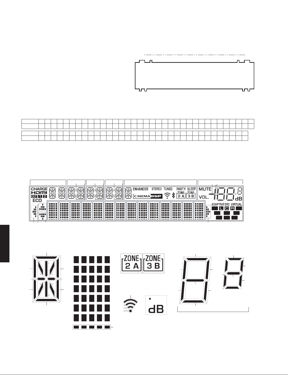
RX-V579/TSR-5790
■ DISPLAY DATA
● V4001 : 020-MT-008GNK (OPERATION P.C.B.)
PATTERN AREA
● PIN CONNECTION
Pin No. 69 68 67 66 65 67 65 62 61 60 59 58 57 56 55 54 53 52 51 50 49 48 47 46 45 44 43 42 41 40 39 38 37 36 35
Connection
F2 NX NP NP P1 P2 P3 P4 P5 P6 P7 P8 P9
Pin No. 34 33 32 31 30 29 28 27 26 25 24 23 22 21 20 19 18 17 16 15 14 13 12 11 10 9 8 7 6 5 4 3 2 1
Connection
P32 P33 P34 P35 P36 P37
Note :
1) F1, F2 ..... Filament pin 2) NP ..... No pin 3) NX ..... No extend pin 4) 1G-20G ..... Grid pin
NX NX NX NX
20G 19G 18G 17G 16G 15G 14G 13G 12G 11G 10G
P10 P11 P12 P13 P14 P15 P16 P17 P18 P19 P20 P21 P22 P23 P24 P25 P26 P27 P28 P29 P30 P31
9G 8G 7G 6G 5G 4G 3G 2G 1G NP NP NX F1
1—
● GRID ASSIGNMENT
S7
S8
RX-V579/TSR-5790
f
e
20G
a1a21a2a1a2a
S9
1G 2G 3G 4G 5G 6G 7G 8G 9G 10G 11G 12G 13G 14G
a
j
hk
nr
p
d
(20G–16G)
19G
col2 col1 col2 col1
1-1 2-1 3-1 4-1 5-1
1-2
b
1-3
mg
1-4
c
1-5
1-6
1-7
2-2
2-3
2-4
2-5
2-6
2-7
3-2
3-3
3-4
3-5
3-6
3-7
18G
17G16G
col2 col1
1a 1a 3aS24a2a
S15 S16
5-2
4-2
5-3
4-3
5-4
4-4
5-5
4-5
4-6
4-7
5-6
5-7
S12
S13
S14
S11
(16G)
(16G)
S17
(15G)
15G
S3
FPRFPL
SL SW SR
SBSBL SBR
S10
a
f
g
e
d
b
c
S4
S5
S5
S6
S4
(15G)
64
S1
(1G–14G)
Page 65
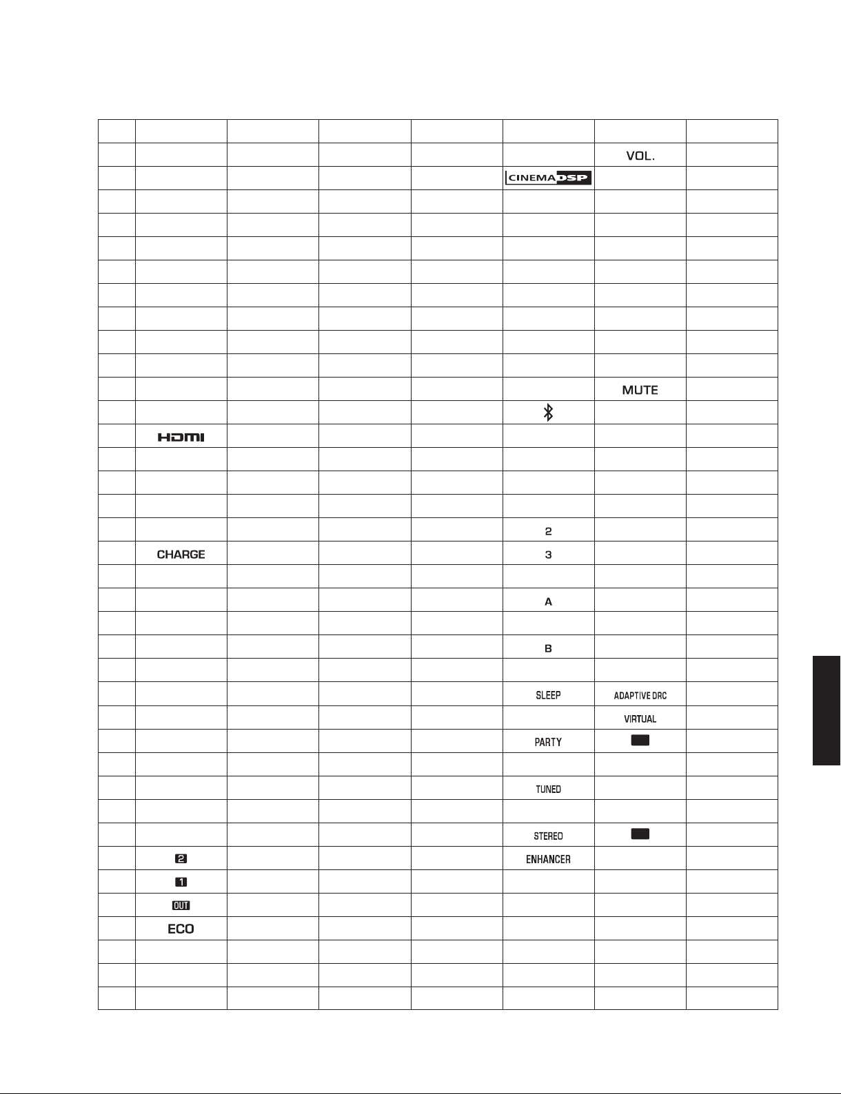
● ANODE CONNECTION
FPL
FPR
20G 19G 18G 17G 16G 15G 1G-14G
P1 1d 1d 1d 1d 1d
RX-V579/TSR-5790
1-1
P2 2d 2d 2d 2d
P3 1e 1e 1e 1e 1e S3 3-1
P4 2e 2e 2e 2e S14 3d 4-1
P5 1r 1r 1r 1r 1r 3e 5-1
P6 2r 2r 2r 2r S13 3c 1-2
P7 1p 1p 1p 1p 1p 3g 2-2
P8 2p 2p 2p 2p S12 3f 3-2
P9 1n 1n 1n 1n 1n 3b 4-2
P10 2n 2n 2n 2n S11 3a 5-2
P11 1c 1c 1c 1c 1c
P12 2c 2c 2c 2c
P13
P14 1g 1g 1g 1g 1g 4c 4-3
P15 2g 2g 2g 2g S16 4g 5-3
P16 1m 1m 1m 1m 1m 4f 1-4
P17 2m 2m 2m 2m
P18
P19 1f 1f 1f 1f 1f S17 4-4
col1 col1 col1 S15 4e 3-3
col2 col2 col2 4a 3-4
S2 2-1
1-3
4d 2-3
4b 2-4
P20 2f 2f 2f 2f
P21 1h 1h 1h 1h 1h S5 1-5
P22 2h 2h 2h 2h
P23 1j 1j 1j 1j 1j S10 3-5
P24 2j 2j 2j 2j
P25 1k 1k 1k 1k 1k
P26 2k 2k 2k 2k
P27 1b 1b 1b 1b 1b A 2-6
P28 2b 2b 2b 2b
P29 1a 1a 1a 1a 1a S 4-6
P30 2a 2a 2a 2a
P31
P32
P33
P34
P35 S8 – – – – K 5-7
P36 S9 – – – – J S1
P37 S7 – – – – – –
– – – F 1-7
– – – – L 2-7
– – – – G 3-7
– – – – H 4-7
S4 5-4
S6 2-5
4-5
5-5
1-6
D 3-6
5-6
RX-V579/TSR-5790
65
Page 66
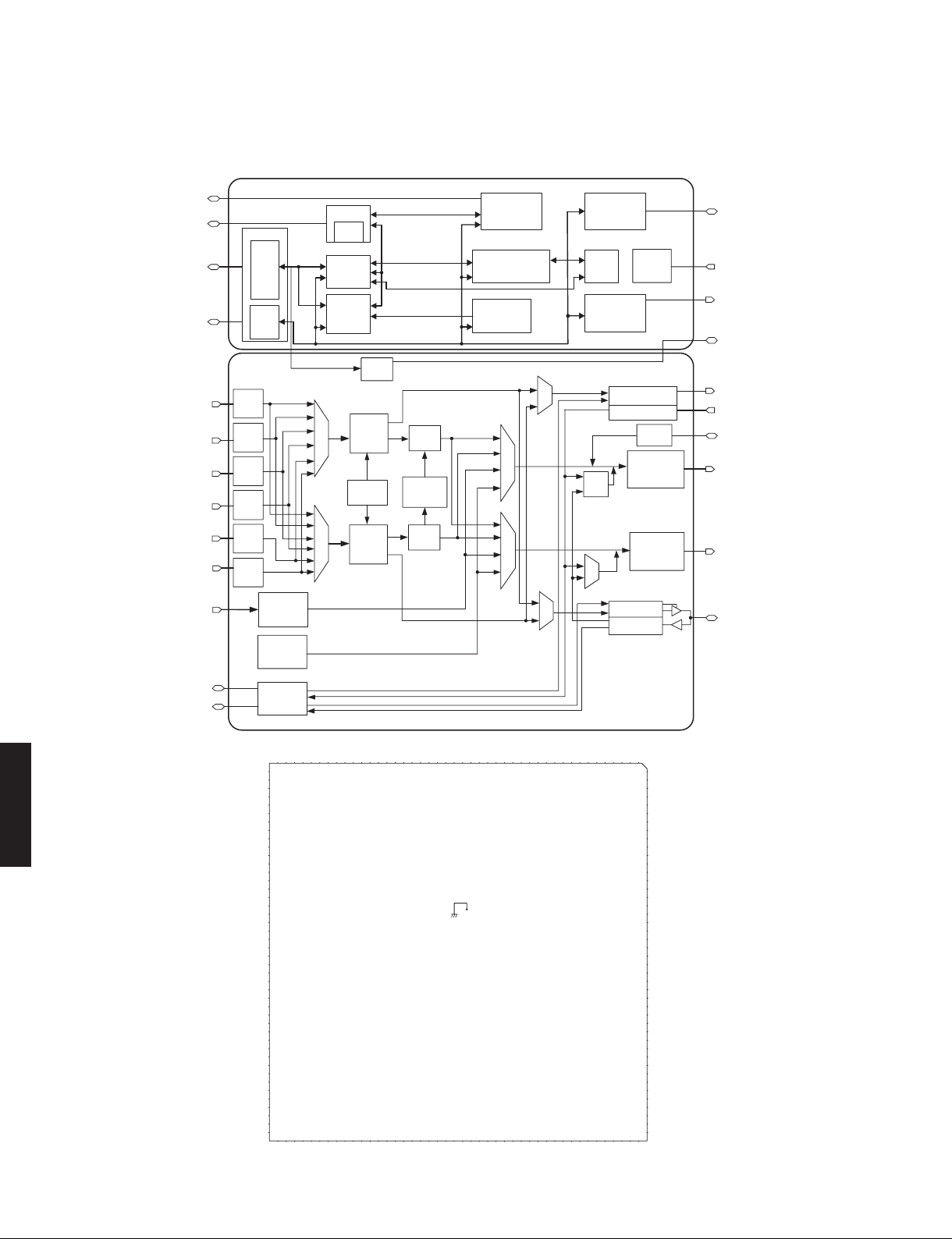
RX-V579/TSR-5790
■ IC DATA
IC1:
SII9573CTUC (DIGITAL P.C.B.)
HDMI port processors
* No replacement part available. / サービス部品供給なし
CEC A0
73
CBUS/
HPD
78,82,86,90,94,99
DDC
I2C
Serial Ports
DDC0
DDC1
DDC2
DDC3
DDC4
DDC5
DDC6
Local
2
I
C
Mobile HD
Control
CBUS0
CBUS1
EDID SRAM
HDCP
Registers
CEC Interface
Controller 0
NVRAM
OTP
Always-On
Section
CEC Interface
Controller 1
Booting
Sequencer
Configuration, Status,
and Interrupt-Control
Registers
Power
72
101
69
CECA1
RnPWR5V,
SBVCC5V
INT
DDC TX
RX-V579/TSR-5790
66
R0X
10-17
R1X
20-27
R2X
28-35
R3X
39-46
R4X
47-54
R5X
57-64
D[19..0]
1-6,161-171,174-176
ARC0/1 Rx
136,137
ARC0/1 Tx
TMDS Rx
(Port 0)
TMDS Rx
(Port 1)
TMDS Rx
(Port 2)
TMDS Rx
(Port 3)
TMDS Rx
(Port 4)
TMDS Rx
(Port 5)
R3X2-
R3X2+
R4XC-
R4XC+
R4X0-
R4X0+
R4X1-
R4X1+
R4X2-
R4X2+
AVDD12
AVDD33
R5XC-
R5XC+
R5X0-
R5X0+
R5X1-
R5X1+
R5X2-
R5X2+
CVCC12
CSDA
RESET#
TPWR_CI2CA
CEC_A1
CEC_A0/WAKEUP
DSDA6(VGA)
DSCL6(VGA)
RSVDL
DSDA0
DSCL0
CBUS_HPD0
R0PWR5V
DSDA1
DSCL1
CBUS_HPD1
R1PWR5V
DSDA2
DSCL2
CBUS_HPD2
R2PWR5V
DSDA3
CSCL
INT
Parallel
Video
Input
Video
Pattern
Generator
ARC
Input
and
Output
45
46
47
48
49
50
51
52
53
54
55
56
57
58
59
60
61
62
63
64
65
66
67
68
69
70
71
72
73
74
75
76
77
78
79
80
81
82
83
84
85
86
87
88
Power-Down
Section
M
U
X
M
U
X
R3XC+
R3X0-
R3X0+
R3X1-
R3X1+
44
89909192939495
DSCL3
DSCL4
DSDA4
R3PWR5V
CBUS_HPD3
R3XC-
CBUS_HPD4
A
B
AVDD33
R4PWR5V
HDMI/
MHL
Receiver
InstaPort
HDCP
Decryption
HDMI/
MHL
Receiver
InstaPort
R2X2-
R2X2+
AVDD12
CVCC12
96979899100
DSCL5
RSVDL
DSDA5
CBUS_HPD5
TPI HW
R2X1+
R5PWR5V
R2X1-
101
SBVCC5V
R2X0-
R2X0+
102
103
VCC33OUT
MHL_CD0/GPIO0
Stream
InstaPrevue
Splitter
R2XC-
R2XC+
293031323334353637383940414243
105
104
TX_HPD0
MHL_CD1/GPIO1
Mixer
Video/
Audio
106
R1X2+
TXDSDA0
R1X2-
107
TXDSCL0
E
M
U
X
C
M
U
X
Audio Output
Multi-Channel
Audio Input
OSD
TMDS Tx
(Port 0) HDCP
SRC
Encryption
Main
Main
I2S/SPDIF/
DSD
76,80,84,88,92,97
I2S/SPDIF
SPI
T0X
151-158
D
Sub
T1X
xT SDMTM
X
F
M
U
X
R0X0-
R0X0+
T0X1-
R0X1+
R0X2-
R0X2+
AVDD12
AVDD33
R1XC-
R1XC+
R1X0-
R1X0+
R1X1-
R1X1+
G
DGND
108
109
110
111
112
113
114
115
116
117
118
119
120
121
XTALIN
APLL12
XTALOUT
XTALVCC33
CVCC12
SS/GPIO2
XTALGND
SDI/GPIO5
SD0/GPIO4
SCLK/GPIO3
WS0_OUT/DR0
TX_HPD1
TXDSCL1
TXDSDA1
R0XC+
122
SCK0/DDCK
R0XC-
10111213141516171819202122232425262728
123
IOVCC33
G
M
U
X
Audio Output
2 Channel
Audio Input
VSYNC
D17
D18
D19
DE
HSYNC
124
125
126
127
128
129
MCLK
SD0_0/DL0
MUTEOUT/GPIO9
SD0_2/DL1/GPIO7
SD0_1/DR1/GPIO6
SD0_3/DR2/GPIO8
)1 troP(U
HDCP Encryption
ENB
Sub
D14
D15
D16
123456789
D13
176
D12
175
D11
174
IOVCC33
173
IDCK
172
D10
171
D9
170
D8
169
D7
168
D6
167
D5
166
D4
165
D3
164
D2
163
D1
162
D0
161
CVCC12
160
TOX2+
159
TOX2-
158
TOX1+
157
TOX1-
156
TOX0+
155
TOX0-
154
TOXC+
153
TOXC-
152
TDVDD12
151
TPVDD12
150
T1X2+
149
T1X2-
148
T1X1+
147
T1X1-
146
T1X0+
145
T1X0-
144
T1XC+
143
T1XC-
142
TDVDD12
141
TPVDD12
140
CVCC12
139
ARC1
138
ARC0
137
SD1_IN/SD1_OUT/SPDIF1_IN/SPDIF1_OUT
136
WS1_IN/WS1_OUT
135
SCK1_IN/SCK1_OUT
134
133
SD0_IN/SPDIFO_IN
130
131
132
WS0_IN/GPIO11
SCK0_IN/GPIO10
SPDIF0_OUT/DL2
141-148
I2S/SPDIF
Page 67
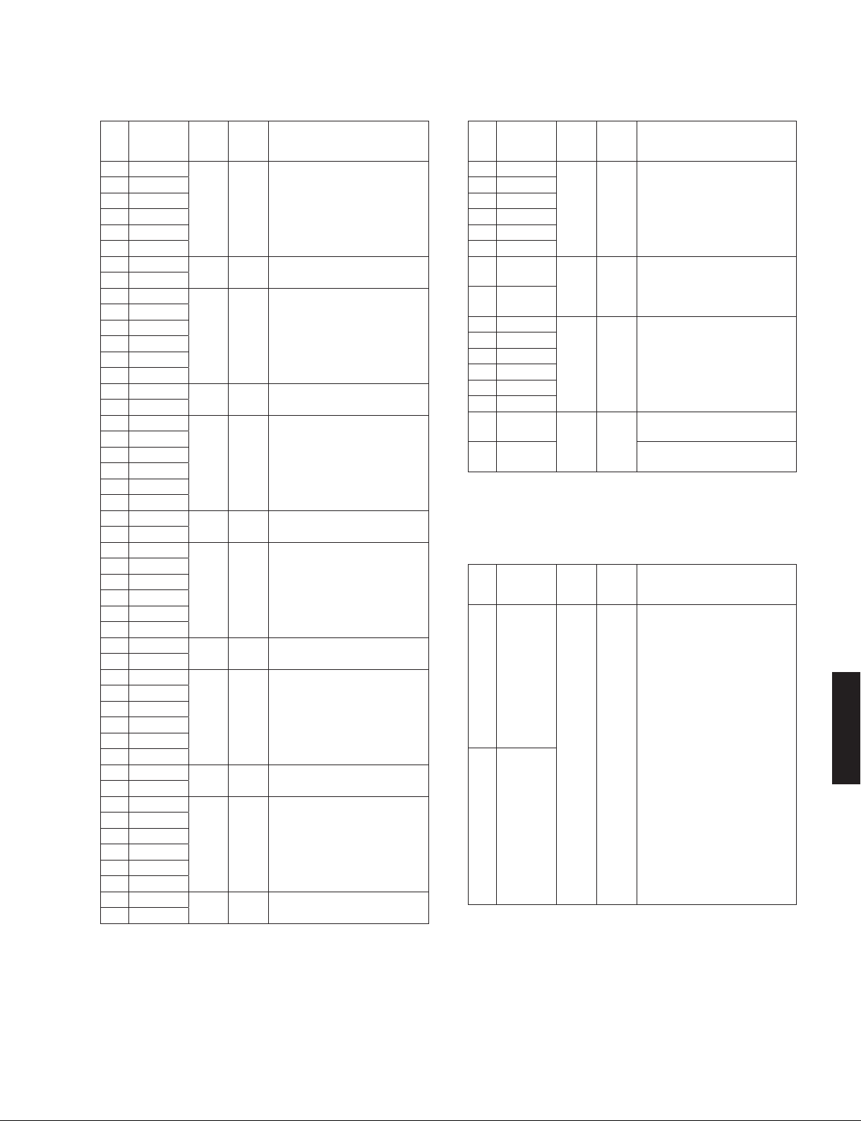
RX-V579/TSR-5790
HDMI Receiver Port Pins
Pin
Function
No.
Name
12 R0X013 R0X0+
14 R0X115 R0X1+
16 R0X217 R0X2+
10 R0XC
11 R0XC+
22 R1X023 R1X0+
24 R1X125 R1X1+
26 R1X227 R1X2+
20 R1XC
21 R1XC+
30 R2X031 R2X0+
32 R2X133 R2X1+
34 R2X235 R2X2+
28 R2XC
29 R2XC+
41 R3X042 R3X0+
43 R3X144 R3X1+
45 R3X246 R3X2+
39 R3XC
40 R3XC+
49 R4X050 R4X0+
51 R4X152 R4X1+
53 R4X254 R4X2+
47 R4XC
48 R4XC+
59 R5X060 R5X0+
61 R5X162 R5X1+
63 R5X264 R5X2+
57 R5XC
58 R5XC+
Type I/O Detail of Function
TMDS Input
TMDS Input
TMDS Input
TMDS Input
TMDS Input
TMDS Input
TMDS Input
TMDS Input
TMDS Input
TMDS Input
TMDS Input
TMDS Input
HDMI receiver Port 0 TMDS input
data pairs.
HDMI receiver Port 0 TMDS input
clock pair.
HDMI receiver Port 1TMDS input
data pairs.
HDMI receiver Port 1 TMDS input
clock pair.
HDMI receiver Port 2 T
data pairs.
HDMI receiver Port 2 TMDS input
clock pair.
HDMI receiver Port 3 TMDS input
data pairs.
HDMI receiver Port 3 TMDS input
clock pair.
HDMI receiver Port 4 TMDS input
data pairs.
HDMI receiv
clock pair.
HDMI receiver Port 5 TMDS input
data pairs.
HDMI receiver Port 5 TMDS input
clock pair.
er Port 4 TMDS input
MDS input
HDMI Transmitter Port Pins
Pin
Function
No.
Name
154 T0X0155 T0X0+
156 T0X1157 T0X1+
158 T0X2159 T0X2+
152 T0XC-
153 T0XC+
144 T1X0145 T1X0+
146 T1X1147 T1X1+
148 T1X2149 T1X2+
142 T1XC-
143 T1XC+
Type I/O Detail of Function
TMDS Output
TMDS Output
TMDS Output
TMDS Output
Audio Return Channel Pins
Pin
Function
No.
Name
137 ARC0
138 ARC1
Type I/O Detail of Function
Analog
Input/
Output
HDMI transmitter Port 0 TMDS
output data pairs.
Main HDMI transmitter output Port
TMDS data pairs.
HDMI transmitter Port 0 TMDS
output clock pair.
Main HDMI transmitter output Port
TMDS clock pair.
HDMI transmitter Port 1 TMDS
output data pairs.
Sub HDMI tra
TMDS data pairs.
HDMI transmitter Port 1 TMDS
output clock pair.
Sub HDMI transmitter output Port
TMDS clock pair.
Audio Return Channels 0 and 1.
These pins are used to transmit
or receive an IEC60958-1 audio
stream. In ARC transmitter mode,
received on the SPDIFn_IN input
pin, this pin transmits an S/
PDIF signal to an ARC receivercapable source (such as HTiB) or
a repeater (such as AVR) devices,
using single-mode ARC.
In ARC receiver
through the SPDIFn_OUT pin,
this pin receives an S/PDIF signal
from an ARC transmitter-capable
sink (such as DTV) device, using
single-mode ARC. In combination
with external components,
common-mode ARC can be
received. Each channel can either
be an ARC input or an ARC output
at one time.
nsmitter output Port
mode, transmitted
RX-V579/TSR-5790
67
Page 68
RX-V579/TSR-5790
Audio Pins
Pin
Function
No.
Name
WS0_OUT/
121
SCK0/
122
DDCK
124 SDO_0/DL0 LVTTL Output
125 MCLK LVTTL Output Master clock output.
SDO_1/
126
DR1/GPIO6
SDO_2/
127
DL1/GPIO7
SDO_3/
128
DR2/GPIO8
MUTEOUT/
129
GPIO9
SPDIF0_
130
OUT/DL2
WS0_IN/
31
1
GPIO11
SCK0_IN/
132
GPIO10
SD0_IN/
133
SPDIF0_IN
SCK1_IN/
134
SCK1_OUT
WS1_IN/
135
WS1_OUT
SD1_IN/
SD1_OUT/
136
SPDIF1_IN/
SPDIF1_
Crystal Pins
Pin
Function
No.
RX-V579/TSR-5790
Name
113 XTALOUT
114 XTALIN
DR0
OUT
Type I/O Detail of Function
LVTTL Output
LVTTL Output
LVTTL Output
LVTTL Output
LVTTL Output
LVTTL
Analog/
LVTTL
LVTTL
LVTTL
Analog/
LVTTL
LVTTL
LVTTL
LVTTL
Type I/O Detail of Function
LVTTL
5 V
tolerant
LVTTL
5 V
tolerant
Main port I2S word select output/
DSD data right bit 0.
Main port I2S serial clock output/
DSD clock output.
Main port I2S serial data 0 output/
DSD data left bit 0 output.
Main port I2S serial data 1 output/
DSD data right
programmable GPIO 6.
Main port I2S serial data 2
output/DSD data left bit 1 output/
programmable GPIO 7.
Main port I2S serial data 3
output/DSD data right bit 2/
programmable GPIO 8.
Input/
Mute audio output/programmable
Output
GPIO 9.
Main port S/PDIF output/DSD data
Output
left bit 2.
Input/
Main port I2S word select input/
Output
programmable GPIO 11.
Input/
Main port I2S serial clock input/
Output
programmable GPIO 10.
Main port I2S serial data input/S/
Input
PDIF input.
Input/
Sub port I2S serial clock1 input/
Output
I2S serial bit clock output.
Input/
Sub port I2S wo
word select output.
Output
Sub port I2S serial data input/I2S
Input/
serial data1 output/ SPDIF input//
Output
SPDIF output.
Output Crystal clock output.
Input Crystal clock input.
bit 1 output/
rd select input/I2S
SPI Interface Pins
Pin
Function
No.
Name
117 SS/GPIO2 LVTTL
SCLK/
118
GPIO3
119 SDO/GPIO4
120 SDI/GPIO5
Type I/O Detail of Function
Input/
SPI slave select/programmable
Output
GPIO 2.
LVTTL
Schmitt
Schmitt
Schmitt
Open
drain
LVTTL
Open
drain
LVTTL
Open
drain/
Input/
SPI clock/programmable GPIO 3.
Output
Input/
SPI slave data output/master data
Output
input/programmable GPIO 4.
Input/
SPI slave data input/master data
Output
output/programmable G
Parallel Video Bus
Pin
Function
No.
Name
1 D14
2 D15
3 D16
4 D17
5 D18
6 D19
161 D0
162 D1
163 D2
164 D3
165 D4
166 D5
167 D6
168 D7
169 D8
170 D9
171 D10
174 D11
175 D12
176 D13
7 DE LVTTL Input Data enable input.
9 HSYNC LVTTL Input Horizontal sync input.
8 VSYNC
172 IDCK LVTTL Input Input data clock.
Type I/O Detail of Function
Video data inputs.
LVTTL Input
LVTTL Input Vertical sync input.
The video data inputs can be
configured to support a wide
variety of input formats, including
multiple RGB and YCbCr bus
formats, using register settings.
PIO 5.
68
Page 69
System Switching Pins
RX-V579/TSR-5790
Pin
No.
76 DSDA0
80 DSDA1
84 DSDA2
88 DSDA3
92 DSDA4
97 DSDA5
73 DSDA6(VGA)
77 DSCL0
81 DSCL1
85 DSCL2
89 DSCL3
93 DSCL4
98 DSCL5
74 DSCL6(VGA)
106 TXDSDA0
109 TXDSDA1
107 TXDSCL0
110 TXDSCL1
79 R0PWR5V
83 R1PWR5V
87 R2PWR5V
91 R3PWR5V
95 R4PWR5V
100 R5PWR5V
78 CBUS_
82 CBUS_HPD1
86 CBUS_HPD2
90 CBUS_HPD3
94 CBUS_HPD4
99 CBUS_HPD5
105 TX_HPD0 LVTTL 5 V tolerant Input Hot plug detect input for HDMI transmitter Port 0.
108 TX_HPD1 LVTTL 5 V tolerant Input Hot plug detect input for HDMI transmitter Port 1.
103 MHL_CD0/GP
104 MHL_CD1/GPIO1 LVTTL Input/Output MHL cable detect 1/programmable GPIO 1.
Function Name Type I/O Detail of Function
LVTTL Schmitt Open
drain 5 V tolerant
LVTTL Schmitt Open
drain 5 V tolerant
LVTTL Schmitt Open
drain 5 V tolerant
LVTTL Schmitt Open
drain 5 V tolerant
LVTTL Schmitt Open
drain 5 V tolerant
LVTTL Schmitt Open
drain 5 V tolerant
VTTL Schmitt Open
L
drain 5 V tolerant
LVTTL Schmitt Open
drain 5 V tolerant
Power Input
HPD0
LVTTL 1.5 mA 5 V
tolerant Analog
IO0 LVTTL Input/Output MHL cable detect 0/programmable GPIO 0.
Input/Output
Input/Output
Input
Input
Input/Output
Input/Output
Input/Output
Input/Output
DDC I2C data for respective HDMI receiver port.
These signals are true open drain, and do not pull to ground when power is
not applied to the device. These pins require an external pull-up resistor.
DDC I2
C data for VGA port.
This signal is true open drain, and does not pull to ground when power is not
applied to the device. This pin requires an external pull-up resistor.
DDC I2C clock for respective HDMI receiver port.
These signals are true open drain, and do not pull to ground when power is
not applied to the device. These pins require an external pu
DDC I2C clock for VGA port.
This signal is true open drain, and does not pull to ground when power is not
applied to the device. This pin requires an external pull-up resistor.
DDC master I2C data for HDMI transmitter Port 0.
This signal is
applied to the device. This pin requires an external pull-up resistor.
DDC master I2C data for HDMI transmitter Port 1.
This signal is true open drain, and does not pull to ground when power is not
applied to the device. This pin requires an external pull-up resistor.
DDC master I2C clock for HDMI transmitter Port 0.
This signal is true open drain, and does not pull to ground when power is not
applied to the device. This pin requires an external pull-up resistor.
DDC master I2C clock for HDMI transmitter Port 1.
This signal is true open drain, and does not pu
applied to the device. This pin requires an external pull-up resistor.
5 V port detection input for respective HDMI receiver port.
Connect to 5 V signal from HDMI input connector. These pins require a
10ohms series resistor, a 5.1 k-ohms pull down resistor, and at least a 1 μ F
capacitor to ground.
Hot plug detect output for the respective HDMI receiver port.
In MHL mode, these pins serve as the respective CTRL bus.
true open drain, and does not pull to ground when power is not
ll-up resistor.
ll to ground when power is not
RX-V579/TSR-5790
69
Page 70
RX-V579/TSR-5790
Control Pins
Pin
No.
66 CSCL
67 CSDA
69 RESET# Schmitt Input
Function Name Type I/O Detail of Function
Schmitt Open drain
5V tolerant
LVTTL Schmitt Open
drain 5 V tolerant
Input
Input/Output
Configuration Pins
Pin
No.
70 TPWR_CI2CA LVTTL Input/Output
68 INT
Function Name Type I/O Detail of Function
Schmitt Open drain
8mA 3.3 V tolerant
Output
Local configuration/status I2C clock.
Chip configuration/status is accessed via this I2C port. This pin is true open
drain, so it does not pull to ground if power is not applied.
Local configuration/status I2C data.
Chip configuration/status is accessed via thi
drain, so it does not pull to ground if power is not applied.
External reset.
Active LOW. Must be pulled up to VCC33OUT. When main power is not
provided to the system, the microprocessor must present a high impedance
of at least 100 k-ohms to RESET#. If this condition is not met, a circuit to
block the leakage from VCC33OUT to the microprocessor
required.
I2C slave address input / Transmit power sense output.
During power-on-reset (POR), this pin is used as an input to latch the I2C
subaddress. The level on this pin is latched when the POR transitions from
the asserted state to the de-asserted state.
After completion of POR, this pin is used as the TPWR output. A register
ng can change this pin to show if the active port is receiving a TMDS
setti
clock.
Interrupt output.
This is an open-drain output and requires an external pull-up resistor.
s I2C port. This pin is true open
GPIO may be
CEC Pins
Pin
No.
72 CEC_A0
RX-V579/TSR-5790
71 CEC_A1
Function Name Type I/O Detail of Function
Primary CEC I/O used for interfacing to CEC devices This signal is electrically
compliant with the CEC specification.
As an input, this pin acts as an LVTTL schmitt triggered input and is 5 V
tolerant.
CEC Compliant 5V
tolerant, Schmitt
triggered, LVTTL
CEC Compliant 5V
tolerant, Schmitt
triggered, LVTTL
Input/Output
Input/Output
As an output, the pin acts as an NMOS driver with resistive pull-up.
This pin has an
This signal should be connected to the CEC signal of all HDMI input and
output ports if the system supports just one CEC line.
OR
In a system designed to have separate CEC connectivity for the HDMI input
and output ports, this signal should be connected to the CEC signal of all the
input ports supported in the system.
This signal and CEC_A0 each connect to a separate CEC co
the port processor and are independent of each other.
Secondary CEC I/O used for interfacing to CEC devices.
This signal is electrically compliant with the CEC specification. As an input,
this pin acts as an LVTTL schmitt triggered input and is 5 V tolerant. As an
output, the pin acts as an NMOS driver with resis
internal pull-up resistor.
This is an optional CEC signal provided for system designers who want to
implement a system with two independent CEC lines, such as a system that
supports a separate CEC line for the HDMI input ports and the HDMI output
ports. In the example of a DTV that provides a second HDMI output using the
SiI957n port processor; this signal can be conne
output port while the CEC_A1 signal is connected to the CEC signal of the
input ports.
This signal and CEC_A1 each connect to a separate CEC controller within
the port processor and are independent of each other.
internal pull-up resistor.
ntroller within
tive pull-up. This pin has an
cted to the CEC signal of the
70
Page 71
Power and Ground Pins
RX-V579/TSR-5790
Pin
No.
19
56
123
173
101 SBVCC5 Power 5.0 V
18
55
37
65
116
139
160
111 APLL13 Power 1.3 V PLL analog VCC.
102 VCC33OUT Power 3.3 V Internal regulator 3.3 V output.
140
150
141
151
112 XTALVCC33 Power 3.3 V PLL crystal oscillator power.
115 XTALGND Ground GND PLL crystal oscillator ground.
ePad GND Ground GND
Function Name Type I/O Detail of Function
AVDD33 Power 3.3 V TMDS core VDD.38
IOVCC33 Power 3.3 V I/O VCC.
Local power from system.
This pin requires a 10 ohms series resistor.
AVDD13 Power 1.3 V TMDS receiver core VDD.36
CVCC13 Power 1.3 V Digital core VCC.
TPVDD13 Power 1.3 V Ana
TDVDD13 Power 1.3 V Digital power for TMDS Tx core.
log power for TMDS Tx core.
The ePad must be soldered to ground, as this is the only ground connection
for the device.
Configuration Pins
Pin
No.
75
96
Function Name I/O Detail of Function
RSVDL Reserved Reserved, must be tied to ground.
RX-V579/TSR-5790
71
Page 72
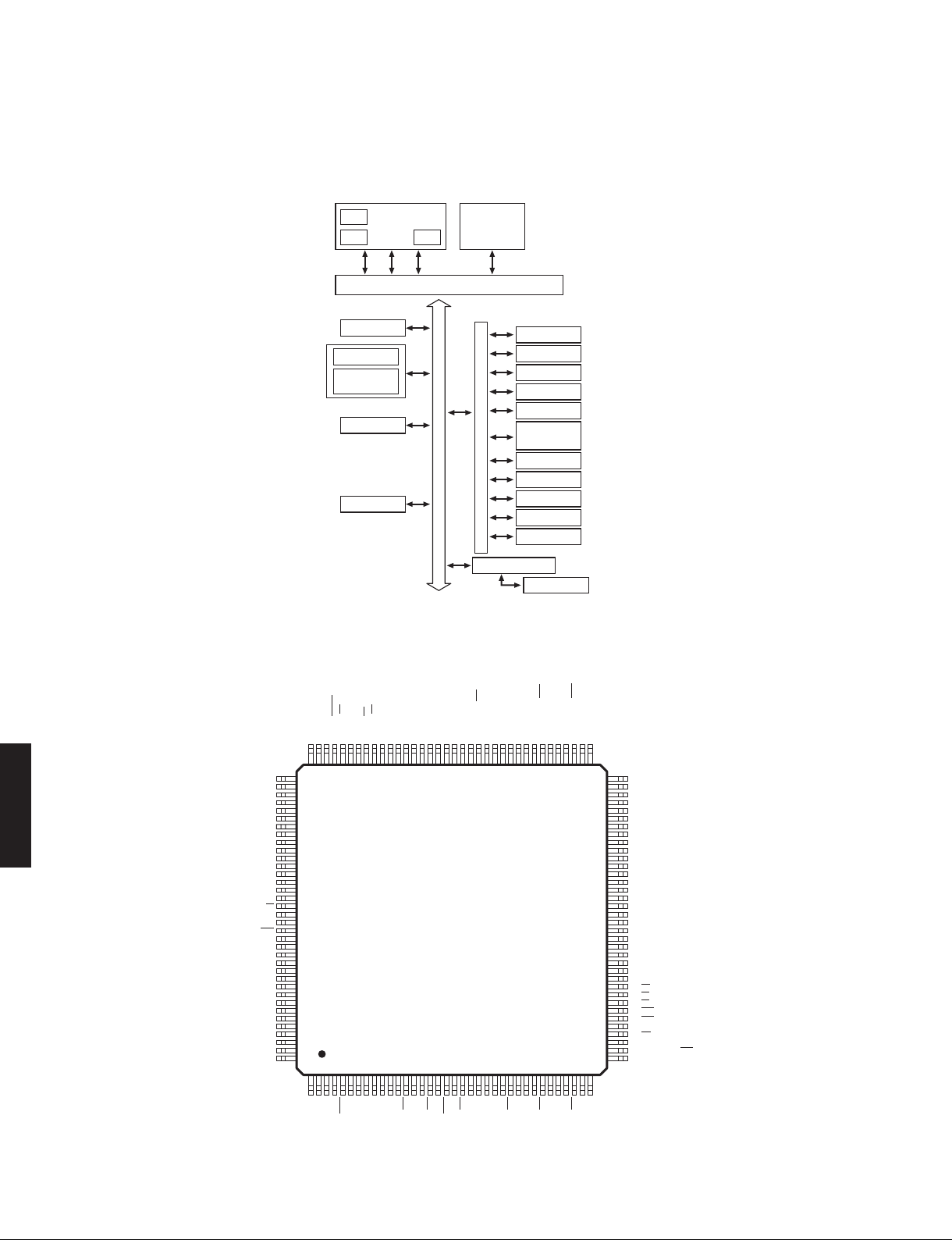
RX-V579/TSR-5790
IC21:
TMPM362F10FG (DIGITAL P.C.B.)
Microprocessor
* No replacement part available. / サービス部品供給なし
ETM
SWD
Cortex-M3
NVIC
AHB Lite Bus Matrix
DMA
Controller
RAM (56KB)
BackupRAM
PH0/SDA3/SO3/TBAIN0
PH2/SCK3/TBBIN0
PH1/SCL3/SI3/TBAIN1
PG7/INT7/WDTOUT
FLASH (1MB)
(8KB)
SMC
BOOT ROM
PG5/SCL2/SI2/TB9IN1
PG4/SDA2/SO2/TB9IN0
PG6/SCK2/CS3
PG3/INT6/CS1
PG2/SCK1/CS0
PF3/TRACEDATA2
PF2/TRACEDATA1
PF4/TRACEDATA3
PG1/SCL1/SI1/TB7IN1
PG0/SDA1/SO1/TB7IN0
AHB Lite Bus 0
PF0/TRACECLK
PF1/TRACEDATA0/SWV
SWDIO
DVDD3B
DVSS
SWCLK
AHB to I/O Bridge
AHB to APB Bridge
PE7/INT5/SCOUT
PE5/A22/RXD0
PE4/A21/TXD0
PE1/A18/TB5IN1
PE6/A23/SCLK0/CTS0
PE2/A19/TB6IN0
PE3/A20/TB6IN1
CG
PORT
WDT
RTC
16bit Timer
SIO/UART
(4byte FIFO)
I2C/SIO
10bit ADC
CEC
RMC
KWUP
SSP
PE0/A17/TB5IN0
PD7/A16/INTB
PD5/A14/RXD11
PD6/A15/SCLK11/CTS11
PD4/A13/TXD11
PD1/A10/RXD10
PD2/A11/SCLK10/CTS10
PD3/A12
PD0/A9/TXD10
RX-V579/TSR-5790
72
TMPM362F10FG
Top View
60
55
50
PC6/A7/SCLK9/CTS9
PC5/A6/RXD9
PC4/A5/TXD9
PC3/A4
PC2/A3/SCLK8/CTS8
PC1/A2/RXD8
PC0/A1/TXD8
PB7/D15/AD15
PB6/D14/AD14
PB5/D13/AD13
PB4/D12/AD12
PB3/D11/AD11
PB2/D10/AD10
PB1/D9/AD9
PB0/D8/AD8
PA7/D7/AD7
PA6/D6/AD6
PA5/D5/AD5
PA4/D4/AD4
PA3/D3/AD3
PA2/D2/AD2
PA1/D1/AD1
PA0/D0/AD0
DVSS
DVDD3B
PP6/ALE
PP5/OE/SPFSS
PP4/WE/SPCLK
PP3/BLS1/SPDI
PP2/BLS0/SPDO
PP1
PP0/CS2
PO7/INTA/TBFOUT
PO6/SCLK7/TBEOUT/CTS7
PO5/RXD7/TBDOUT
Page 73
RX-V579/TSR-5790
I/O
Pin
No.
1 PK6/AIN14 N_FCT AD I+ I+ I FCT detection
2 PK7/AIN15 HDMI_N_INT I I I I Interrupt input from HDMI RxTx
3 AVSS AVSS MCU MCU MCU MCU Microprocessor ground
4 VREFH VREFH MCU MCU MCU MCU Microprocessor power supply
5 /RESET CPU_N_RST MCU MCU MCU MCU Reset input
6 MODE MODE MCU MCU MCU MCU Mode terminal (GND)
7 PL0/SDA0/SO0/TB0OUT HDMI_SDA SIO HiZ HiZ HiZ HDMI Rx/Tx
8 PL1/SCL0/SI0/TB1OUT HDMI_SCL SO HiZ HiZ HiZ HDMI Rx/Tx 12C SCL output
9 PL2/SCK0/TB2OUT HDMI_N_RST O O HiZ O HDMI RxTx reset
10 PL3/INT0/TB3OUT HDMI_N_INTR I I I I Interrupt input from HDMI RxTx bridge IC
11 PL4/TXD1/TB4OUT DSP_MOSI SO O O O DSP, DIR, DAC synchronization data output
12 PL5/RXD1/TB5OUT DSP_MISO SI I I I DSP, DIR synchronization data input
13 PL6/SCLK1/TB6OUT//CTS1 DSP_SCK SO HiZ HiZ HiZ DSP, DIR, DAC
14 PL7/INT1/TB7OUT DSP_N_INT IRQ I I I Interrupt input from DSP
15 DVSS DVSS MCU MCU MCU MCU Microprocessor ground
16 PM0/SCLK2/TB1N0//CTS2 DIR_N_CS O O O O DIR chip select
17 PM1/TXD2/TB1N1 DIR_N_RST O O HiZ HiZ DIR reset
18 PM2/RXD2//ALARM DSP_N_CS O O O O DSP chip select
19 PM3/INT2/TB3OUT DIR_N_INT IRQ I I I DIR interrupt input
20 PM4/SCLK3//CTS3 DSP_N_RST O O HiZ O DSP reset
21 PM5/TXD3 DSP_N_RDY I+ I I I DSP Ready input
22 PM6/
23 PM7/INT3 DAC_N_CS O O O O DAC chip select
24 PN0/TXD4 FLASH_TXD SO HiZ HiZ HiZ Serial port for F/W writing
25 PN1/RXD4 FLASH_RXD SI I+ I+ I Serial por t for F/W writing
26 PN2/SCLK4/TB2IN0//CTS4 232C_N_CTS I+ I+ I+ I Serial port for F/W writing
27 PN3/INT4/TB2IN1/RMC0 REM_IN IRQ IRQ IRQ IRQ Remote control pulse input
28 PN4/TXD5 232C_RTS O O O O Serial port for F/W writing
29 PN5/RXD5 NCPU_ADT_MUTE I-
30 PN6/SCLK5/TBFIN0//CTS5 HDMI_N_RSTRT I+ I I I HDMI Rx/Tx (Rouge) reset
31 PN7/INT8/TBFIN1/RMC1 PSW_N_DET IRQ IRQ IRQ IRQ Power system switch (Power, Scene) detection
32 PO0/TXD6/TB8OUT NCPU_SPI_MOSI SO O HiZ O NET SPI data output
33 PO1/RXD6/TB9OUT NCPU_SPI_MISO SI I I I NET SPI data input
34
35 PO3/INT9/TBBOUT NCPU_SPI_N_CS O O O O NET SPI chip selec
36 PO4/TXD7/TBCOUT NCPU_N_RST O O HiZ O NET CPU reset output
37 PO5/RXD7/TBDOUT NCPU_MODE I- I- I- I-
38
39 PO7/INTA/TBFOUT AMP_LMT
40 PP0//CS2 DIR_SDO I I I I DIR, SDO input for CDDA writing
41 PP1 DIR_WCK I I I I DIR, WCK input for CDDA writing
42 PP2//BLS0/SPDO OSDFS_MOSI SO O HiZ O OSD Flas
43 PP3//BLS1/SPDI OSDFS_MISO SI I- I- I- OSD Flash synchronization data input
44 PP4//WE/SPCLK OSDFS_SCK SO O O O OSD Flash synchronization clock output
45 PP5//OE/SPFSS OSDFS_N_CS O HiZ HiZ HiZ OSD Flash chip select control from Microprocessor
46 PP6//ALE OSDFS_BUS_SEL O O HiZ O
47 DVDD3B DVDD3B MCU MCU MCU MCU Microprocessor powe
48 DVSS DVSS MCU MCU MCU MCU Microprocessor ground
Port Name
RXD3 DSP_FMT O HiZ HiZ HiZ DSP Full Mute output
PO2/SCLK6/TBAOUT//CTS6
PO6/SCLK7/TBEOUT//CTS7
Function Name
(P.C.B.)
Full on
NCPU_SPI_SCK SO O O O NET SPI clock output
NDAC_N_MT O O O O Mute control
DA(PWM)
Power off
I- I- I- NET SPI mute request
O O O Limiter control output
MCU sleep
AC off
+3.3V: Normal operation / 0V: MAC address writing
permission
Connection switching of Microprocessor SPI and HDMI
OSD SPI to OSD Flash SPI
Detail of Function
12C SDA input and output
synchronization clock output
h synchronization data output
t output
r supply
RX-V579/TSR-5790
73
Page 74
RX-V579/TSR-5790
Pin
No.
49 PA0/D0/AD0 PRY O O O O Power relay control
50 PA1/D1/AD1 TRANS_RY O O HiZ O Switching transformer winding
51 PA2/D2/AD2 HPRY O O HiZ O Headphone relay control
52 PA3/D3/AD3 SPRY_5CH O O HiZ O Speaker relay control (Front/Center/Surround)
53 PA4/D4/AD4 SPRY_SB_BA O O O O Speaker relay control (Surround back & Bi-Amp)
54 PA5/D5/AD5 DIAG_FCT O O O O Diag
55 PA6/D6/AD6 MT_N_5CH O O HiZ O Mute control (Front/Center/Surround)
56 PA7/D7/AD7 MT_N_SB O O O O Mute control (Surround back)
57 PB0/D8/AD8 MT_N_SW O O HiZ O Mute control (Subwoofer)
58 PB1/D9/AD9 NDASW_SEL O O O O L: NET module output 1 / H: NET module output 2
59 PB2/D10/AD10 +3.3S_PON O O O O
60 PB3/D11/AD11 HDMI_PON O O HiZ O
61 PB4/D12/AD12 DCDC_PON O O HiZ O
62 PB5/D13/AD13 DSP_PON O O HiZ O
63 PB6/D14/AD14 NCPU_PON O O HiZ O
64 PB7/D15/AD1
65 PC0/A1/TXD8 NCPU_RXD SO O HiZ O NET CPU UART 4
66 PC1/A2/RXD8 NCPU_TXD SI I I I NET CPU UART 4
67 PC2/A3/SCLK8//CTS8 NCPU_VBUSDRV O O HiZ O
68 PC3/A4 USB_VBUS_PON I I I I USB power supply output control
69 PC4/A5/TXD9 NCPU_PHOLD O O O O
70 PC5/A6/RXD9 VOL_SCK O O O O Electronic volume flip-flop synchronization clock output
1 PC6/A7/SCLK9//CTS9 VOL_MOSI O O O O Electronic volume flip-flop synchronization data output
7
72 PC7/A8 EEP_SPI_N_CS O O HiZ O EEPROM chip select
73 PD0/A9/TXD10 EEP_SPI_MOSI SO SO O SO EEPROM synchronization data output
74 PD1/A10/RXD10 EEP_SPI_MISO SI SI I SI EEPROM synchronization data input
75 PD2/A11/SCLK10//CTS10 EEP_SPI_SCK O O O O EEPROM synchronization clock output
76 PD3/A12 CVBS_ON O O HiZ O Video SW
77 PD4/A13/TXD11 CPNT_ON O O HiZ O Video S
78 PD5/A14/RXD11 O O O O
79 PD6/A15/SCLK11//CTS11 NCPU_MUTE_REQ0 O O O O NET audio mute request
RX-V579/TSR-5790
80 PD7/A16/INTB NCPU_MUTE_REQ1 I I I I NET audio mute request
81 PE0/A17/TB5IN0 ADT_N_EN I+ I+ I+ I
82 PE1/A18/TB5IN1 ADT_SEL O O O O
83 PE2/A19/TB6IN0 FLD_N_RST O O O O FL driver reset
84 PE3/A20/TB6IN1 FLD_N_CS O O O O FL driver chip select
85 PE4/A21/TXD0 FLD_MOSI SO O O O FL driver synchronization data output
86 PE5/A22/RXD0 FL_PON O O HiZ O FL driver +VP control output
87 PE6/A23/SCLK0//CTS0 FLD_SCK SO O O O FL driver synchronization clock output
88 PE7/INT5/SCOUT HDMI_N_INTT I I I I Interrupt input from HDMI Tx bridge IC
89 DVDD3B DVDD3B MCU MCU MCU MCU Microprocessor power supply
90 DVSS DVSS MCU MCU MCU MCU Microprocessor ground
91 SWDIO SWD_IO MCU MCU MCU MCU Terminal for debuggin
92 SWCLK SWD_SCK MCU MCU MCU MCU Terminal for debugging
93 PF0/TRACECLK (reserved)
94 PF1/TRACEDATA0/SWV SWD_SWV MCU MCU MCU MCU Terminal for debugging
95 PF2/TRACEDATA1 VSEL1 O O O O Video selector control signal level conversion
I/O
Port Name
5 VID_PON O O O O
Function Name
(P.C.B.)
Full on
Power off
Detail of Function
MCU sleep
AC off
OK: output High
USB power supply output request from NET
microprocessor
Power supply control IC in NET module output control
W
NET DAC input control for preventing NET DAC
mulfunction
NET module upstream select
L: DSP output / H: DIR output
g
74
Page 75
RX-V579/TSR-5790
I/O
Pin
No.
96 PF3/TRACEDATA2 VSEL2 O O O O Video selector control signal level conversion
97 PF4/TRACEDATA3 O O O O (Reserved) switching I2C to Tuner
98 PG0/SDA1/SO1/TB7IN0 TUN_SDA SIO HiZ HiZ HiZ Tuner I2C synchronization data input and output
99 PG1/SCL1/SI1/TB7IN1 TUN_SCL SO HiZ HiZ HiZ Tuner I2C synchronization clock output
100 PG2/SCK1//CS0 TUN_N_
101 PG3/INT6//CS1 TUN_N_INT IRQ I I I Tuner GPIO2 input
102 PG4/SDA2/SO2/TB9IN0 SIO HiZ HiZ HiZ USB I2C synchronization data input and output
103 PG5/SCL2/SI2/TB9IN1 SO HiZ HiZ HiZ USB I2C synchronization clock output
104 PG6/SCK2//CS3 VOL_RA I+ I+ I+ I Volume rotary encoder A
105 PG7/INT7//WDTOUT VOL_RB I+ I+ I+ I Volume rotary encoder B
106 PH0/SDA3/SO3/TBAIN0 AVID_SDA O O O O Video IC I2C data input and output
107 PH1/SCL3
108 PH2/SCK3/TBBIN0 HP_N_DET I+ I I I Headphone detection
109 PH3/INTC/TBBIN1 MIC_N_DET I+ I I I MIC detection
110 PH4/SDA4/SO4/TBDIN0 STBY_LED SIO HiZ HiZ HiZ Standby through LED, H: LED lighting
111 PH5/SCL4/SI4/TBDIN1 SO HiZ HiZ HiZ
112 PH6/SCK4/TBEIN0 VID_I2C_ON O O HiZ O Video and Audio Selector I2C line control
113 PH7/INTD/TBEIN1 HDMI_MUTE IRQ I- I- I- HDMI MUTE input
114 RVDD3 RV
115 XT1 XT1 MCU MCU MCU MCU Low frequency oscillation circuit input
116 XT2 XT2 MCU MCU MCU MCU Low frequency oscillation circuit output
117 DVDD3A DVDD3A MCU MCU MCU MCU Microprocessor power supply
118 X1 X1 MCU MCU MCU MCU High frequency oscillation circuit input
119 DVSS DVSS MCU MCU MCU MCU Microprocessor ground
120 X2 X2 MCU MCU MCU MCU High frequency oscillation circuit output
121 DVDD3B DVDD3B MCU MC
122 DVSS DVSS MCU MCU MCU MCU Microprocessor ground
123 PI2/INTE ACPWR_DET IRQ IRQ IRQ IRQ AC power detection
124 PI3/INTF O O O O
125 /NMI NMI_N_INT IRQ IRQ IRQ IRQ Non-maskable interrupt
126 TEST1 TEST1 Do not connect.
127 TEST2 TEST2 Do not connect.
128 PI0//BOOT FLASH_N_BOOT I+ I+ I+ I L: Single boot mode (boot from built-in MaskROM)
129 PI1/CEC HDMI_CEC IO+ IO+ IO+ HiZ Microprocessor CEC control
130 AVDD3 AVDD3 MCU
131 PJ0/AIN0 I_PRT AD I- I- I- Overcurrent protection detection
132 PJ1/AIN1 DEST Destination discrimination
133 PJ2/AIN2 KEY1 AD I+ I+ I KEY AD value uptake 1
134 PJ3/AIN3//ADTRG KEY2 AD I+ I+ I KEY AD value uptake 2
135 PJ4/AIN4/KWUP0 KEY AD value uptake 3 (spare)
136 PJ5/AIN5/KWUP1 THM1_PRT AD I I I Temperature detection 1
137 PJ6/AIN6/KWUP2 THM2_PRT AD I I I Temperature detection 2
138 PJ7/AIN7/KWUP3 PS1_P
139 PK0/AIN8 PS2_PRT PS protection detection 2
140 PK1/AIN9 PS3_PRT PS protection detection 3
141 PK2/AIN10 DC_PRT AD I I I Power amp DC detection
142 PK3/AIN11 AMP_OLV AD I I I Power amp output level detection
143 PK4/AIN12 USB_VBUS_PRT USB power supply voltage detection
144 PK5/AIN13 Audio output detection
Port Name
/SI3/TBAIN1 AVID_SCL O O O O Video IC I2C clock input and output
Function Name
(P.C.B.)
Full on
RST O O O O Tuner reset
DD3 MCU MCU MCU MCU Microprocessor power supply
RT AD I I I PS protection detection 1
Power off
U MCU MCU Microprocessor power supply
MCU MCU MCU Microprocessor power supply
MCU sleep
AC off
Detail of Function
RX-V579/TSR-5790
75
Page 76
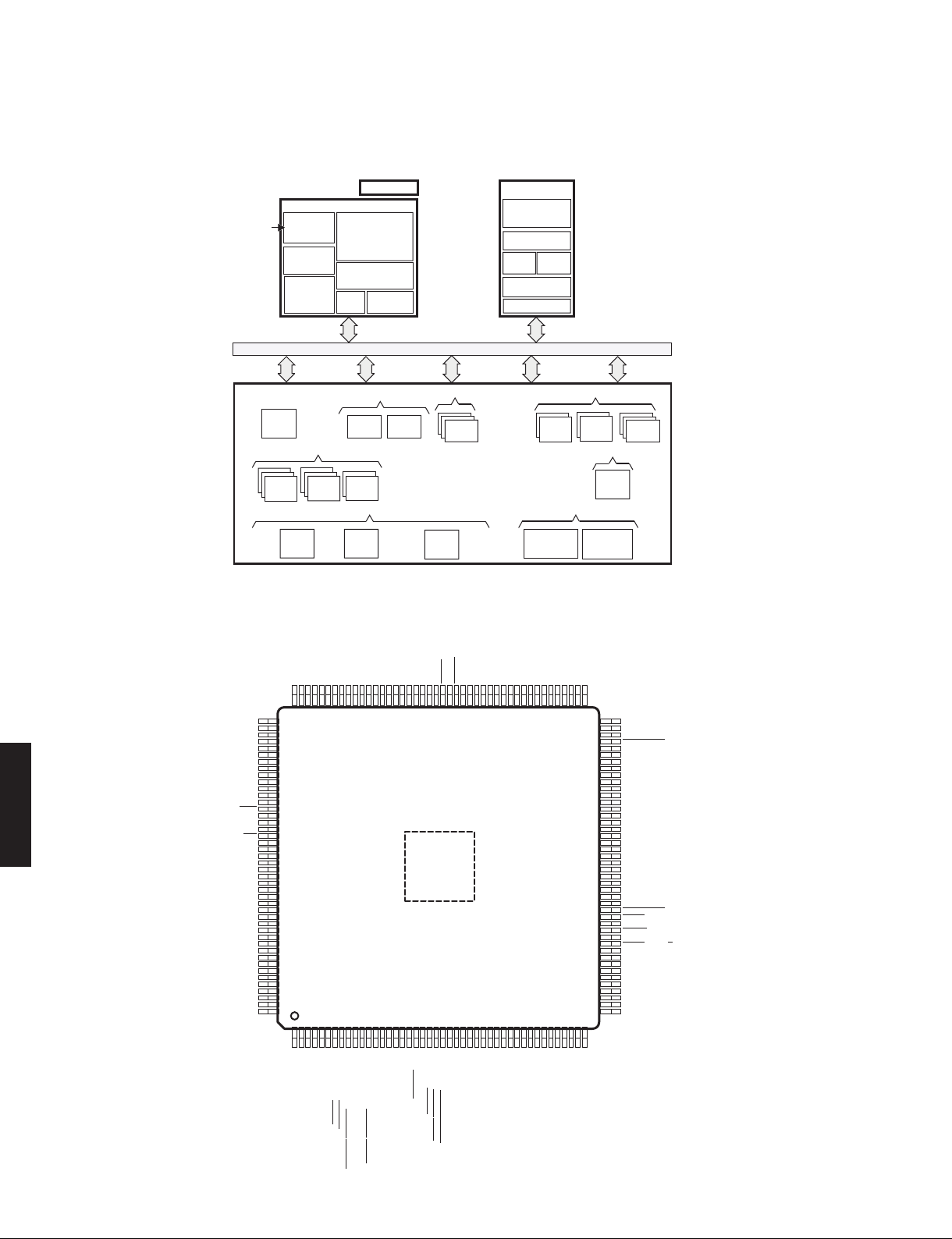
RX-V579/TSR-5790
IC41:
D80YK113DPTP4000 (DIGITAL P.C.B.)
Decoder/Post processor
* No replacement part available. / サービス部品供給なし
Input
Clock(s)
System Control
PLL/Clock
Generator
w/OSC
GeneralPurpose
Timer
GeneralPurpose
Timer
(Watchdog)
JTAG Interface
Memory Protection
Power/Sleep
Controller
RTC/
32-KHz
Multiplexing
OSC
Pin
Switched Central Resource (SCR)
DSPSubsystem
C674x™
DSPCPU
AET
32 KB
32 KB
L1 Pgm
L1 RAM
256 KB L2 RAM
1024 KB L2 ROM
RX-V579/TSR-5790
76
RSV2
USB0_VDDA12
USB0_VDDA18
USB0_DP
USB0_DM
USB0_VDDA33
PLL0_VDDA
PLL0_VSSA
OSCIN
OSCVSS
OSCOUT
RESET
RTC_XI
RTC_CVDD
TRST
GP7[14]
AHCLKX1/EPWM0B/GP3[14]
ACLKX1/EPWM0A/GP3[15]
AFSX1/EPWMSYNCI/EPWMSYNC0/GP4[10]
ACLKR1/ECAP2/APWM2/GP4[12]
AFSR1/GP4[13]
AXR1[8]/EPWM1A/GP4[8]
AXR1[7]/EPWM1B/GP4[7]
AXR1[6]/EPWM2A/GP4[6]
AXR1[5]/EPWM2B/GP4[5]
AXR1[4]/EQEP1B/GP4[4]
AXR1[3]/EQEP1A/GP4[3]
AXR1[2]/GP4[2]
AXR1[1]/GP4[1]
Peripherals
GPIO
eHRPWM
NC
NC
CV
DD
DV
DD
TMS
TDI
CV
DD
TCK
TDO
DV
DD
CV
DD
CV
DD
DV
DD
CV
DD
DV
DD
Control Timers
USB2.0
OTG Ctlr
PHY
]41[4PG/ZTMWPRHE/1ETUMA
]21[3PG/0RSFA
132
131
133
134
135
136
137
138
139
140
141
142
143
144
145
146
147
148
149
150
151
152
153
154
155
156
157
158
159
160
161
162
163
164
165
166
167
168
169
170
171
172
173
174
175
176
1
2
]0[4PG/]0[1RXA
]8[TOOB/]8[5PG/21NI_0P46MT/ADS
_0C2I/DXR_0TRAU
]51[2PG/1MWPA/1PACE/0RKLCA
130
]9[TOOB/]9[5PG/21TUO_0P46MT/LCS_0C2I/DXT_0TRAU
3
eCAP
]11[TOOB/]41[2PG/0RKLCHA
129
4
]01[5PG/]01[1RX
A
DD
VD
128
5
DD
VD
]21[2PG/0MWPA/0PACE/0XKLCA
]01[TOOB/]31[2PG/0XSFA
126
127
7
6
]11[5PG/]11[1RXA
]21[5PG/DXR_2TRAU/ANE_1IPS
EDMA3
eQEP
Connectivity
HPI
]11[2PG/NIKLCFER_BSU/2XKLCHA/0XKLCHA
]01[3PG/]01[0RXA/DXT_1TRAU
]9[3PG/]9[0RXA/DXR_1TRAU
]11[3PG/]0[2RXA/]11[0RXA
125
124
123
122
11
8
9
10
]2[TOOB/]2[5PG/I1PEQE/KLC_0IPS
]31[5PG/DXT_2TRAU/]0[SCS_1IPS
DD
VC
STR_0TRAU ]0[SCS_
/
0IPS ]4[TOOB/]4[5PG/B0PEQE/
DMA
dMAX
Audio Ports
McASP
w/FIFO
Serial Interfaces
2
IC
SPI
UART
Shared Memory
128 KB
RAM
External Memory Interfaces
MMC/SD
(8b)
]6[3PG/2RKLCA/]6[0RXA
]1[3PG/2XKLCA/]1[0RXA
]4[3PG/]1[2RXA/]4[0RXA
]3[3PG/]2[2RXA/]3[0RXA
]2[3PG/]3[2RXA/]2[0RXA
]0[3PG/2RSFA/]0[0RXA
]5[3PG/2XSFA/]5[0RXA
]8[3PG/]8[0RXA
]7[3PG/]7[0RXA
DD
DD
VD
VC
611
511
411
911
811
311
211
711
120
121
Thermal Pad
19
20
12
13
]5[TOOB/]5[5PG/LCS_1C2I/]0[IMOS_1IPS14]6[TOOB/]6[5PG/ADS_1C2I/]0[OMIS_1IPS
STC_0TRAU ANE_
0IPS ]3[TOOB/]3[5PG/A0PEQE//
212223
16
15
17
18
]1[TOOB/]1[5PG/S0PEQE/]0[OMIS_0IPS
]6[2PG/2ETUMA/]3[SC_AME
]0[TOOB/]0[5PG/I0PEQE/]0[IMOS_0IPS
]7[TOOB/]7[
]01[2PG//]0[TIAW_AME YDRH_IPHU
DD
DD
VD
V
C
5PG/S1PEQE/KLC_1IPS
]21[7PG/]01[A_BME
]0[7PG/]1[AB_BME
]
1[7PG/]0[AB_BME
]0[SC_BME
SAR_BME
DD
VD
111
011
108
107
105
106
109
V
SS
(177)
24
25
27
28
26
]51[TOOB/]5[2PG/SCH_IPHU/]2[SC_AME
]31[1PG/LIWHH_IPHU/]1[AB_AME
]01[1PG/]01[A_AME
]41[1PG/]0[
DD
VD
VC
0RXA//
AB_AME
1SDH_IPHU /EO_
A
ME ]7[2PG/]31[
EMIFA(8b/16b)
NAND/Flash
16b SDRAM
]4[7PG/]2[A_BME
]6[7PG/]4[A_BME
]2[7PG/]0[A_BME
DD
VC
104
103
29
30
]0[1PG/]0[A_AME
]1[1PG/0LTNCH_IPHU/KLC_DSCMM/]1[A_AME
DD
]8[7PG/]6[A_BME95]9[7PG/]7[A_BME
]3[7PG/]1[A_BME
]7[7PG/]5[A_BME
]5[7PG/]3[A_BME
DD
VD
98
96
99
97
101
100
102
32
35
36
33
38
31
34
37
]4[1PG/]4[A_AME
]5[1PG/]5[A_AME
]6[1PG/]6[A_AME
]7[1PG/]7[A_AME
]2[1PG/1LTNCH_IPHU/DMC_DSCMM/]2[A_AME
]3[1PG/]3[A_AME
DD
DD
VC
VD
EMIFB
SDRAM Only
(16b/32b)
]31[3PG/]21[A_BME
]31[7PG/]11[A_BME
]01[7PG/]8[A_BME
]11[7PG/]9[A_BME
D
DD
D
VD
VC
94
92
90
89
93
91
88
EMB_SDCKE
87
DV
DD
86
EMB_CLK
85
EMB_WE_DQM[1]/GP5[14]
84
EMB_D[8]/GP6[8]
83
EMB_D[9]/GP6[9]
82
EMB_D[10]/GP6[10]
DV
81
DD
80
EMB_D[11]/GP6[11]
79
EMB_D[12]/GP6[12]
78
EMB_D[13]/GP6[13]
CV
77
DD
76
EMB_D[14]/GP6[14]
DV
75
DD
74
EMB_D[15]/GP6[15]
73
EMB_D[0]/GP6[0]
72
EMB_D[1]/GP6[1]
71
DV
DD
70
EMB_D[2]/GP6[2]
69
CV
DD
68
EMB_D[3]/GP6[3]
67
CV
DD
66
EMB_D[4]/GP6[4]
65
DV
DD
64
EMB_D[5]/GP6[5]
63
EMB_D[6]/GP6[6]
62
EMB_D[7]/GP6[7]
61
CV
DD
60
EMB_WE_DQM[0]/GP5[15]
59
EMB_WE
58
DV
DD
57
EMB_CAS
56
CV
DD
55
EMA_WE W/UHPI_HR /AXR0[12]/GP2[3]/BOOT[14]
54
EMA_D[7]/MMCSD_DAT[7]/UHPI_HD[7]/GP0[7]/BOOT[13]
53
DV
DD
52
EMA_D[6]/MMCSD_DAT[6]/UHPI_HD[6]/GP0[6]
51
EMA_D[5]/MMCSD_DAT[5]/UHPI_HD[5]/GP0[5]
50
CV
DD
49
EMA_D[4]/MMCSD_DAT[4]/UHPI_HD[4]/GP0[4]
48
EMA_D[3]/MMCSD_DAT[3]/UHPI_HD[3]/GP0[3]
47
DV
DD
46
EMA_D[2]/MMCSD_DAT[2]/UHPI_HD[2]/GP0[2]
45
EMA_D[1]/MMCSD_DAT[1]/UHPI_HD[1]/GP0[1]
44
39
40
41
42
43
]9[1PG/]9[A_AME
]8[1PG/]8[A_AME
DD
DV
EMA_A[11]/GP1[11]
EMA_A[12]/GP1[12]
EMA_D[0]/MMCSD_DAT[0]/UHPI_HD[0]/GP0[0]/BOOT[12]
Page 77
RX-V579/TSR-5790
No.
1 AXR1[0]/GP4[0] I/O McASP1serial data
2 UART0_RXD/I2C0_SDA/TM64P0_IN12/GP5[8]/BOOT[8] I UART0 receive data
3 UART0_TXD/I2C0_SCL/TM64P0_OUT12/GP5[9]/BOOT[9] O UART0 transmit data
4 AXR1[10]/GP5[10] I/O McASP1serial data
5 DVDD
6 AXR1[11]/GP5[11] I/O McASP1serial data
7 SPI1_ENA/UART2
8 SPI1_SCS[0]/UART2_TXD/GP5[13] I/O SPI1 chip select
9 SPI0_SCS[0]/ UART0_RTS /EQEP0B/GP5[4]/BOOT[4] I/O SPI0 chip select
10 CVDD
11 SPI0_CLK/EQEP1I/GP5[2]/BOOT[2] I/O SPI0 clock
12 SPI0_ENA/ UART0_CTS /EQEP0A/GP5[3]/BOOT[3] I/O SPI0 enable
13 SPI1_SOMI[0]/I2C1_SCL/GP5[5]/BOOT[5] I/O SPI1 data slave-out-master-in
14 SPI1_SIMO[0]/I2C1_SDA/GP5[6]/BOOT[6] I/O SPI1 data slave-in-master-out
15 DVDD
16 SPI1_CLK/EQEP1S/GP5[7]/BOOT[7] I/O SPI1 clock
17 SPI0_SOMI[0]/EQEP0I/GP5[0]/BOOT[0] I/O SPI0 data slave-out-master-in
18 SPI0_SIMO[0]/EQEP0S
19 EMA_WAIT[0]/ UHPI_HRDY /GP2[10] I EMIFA wait input/interrupt
20 CVDD
21 EMA_CS[3]/AMUTE2/GP2[6] O EMIFA Async chip select
22 EMA_OE/UHPI_HDS1/AXR0[13]/GP2[7] O EMIFA output enable
23 EMA_CS[2]/ UHPI_HCS /GP2[5]/BOOT[15] O EMIFA Async chip select
24 DVDD
Function Name
(P.C.B.)
_RXD/GP5[12] I/O SPI1enable
/GP5[1]/BOOT[1] I/O SPI0 data slave-in-master-out
I/O Detail of Function
I/O I2C0 serial data
I Timer0 lower input
I BOOT[8]
I/O I2C0 serial clock
I Timer0 lower output
I BOOT[9]
I UART2 receive data
O UART2 transmit data
O UART0 ready-to-send output
I eQEP0B quadrature input
I BOOT[4]
I eQEP1 index
I BOOT[2]
I UART0 clear-to-send input
I eQEP0A
I BOOT[3]
I/O I2C1 serial clock
I BOOT[5]
I/O I2C1 serial data
I BOOT[6]
I eQEP1 strobe
I BOOT[7]
I eQEP0 index
I BOOT[0]
I eQEP0 strobe
I BOOT[1]
I/O UHPI ready
I/O McASP2 mute output
I/O UHPI data strobe
I/O McASP0 serial data
I/O UHPI chip select
I BOOT[15
quadrature input
]
RX-V579/TSR-5790
77
Page 78
RX-V579/TSR-5790
No.
25 EMA_BA[0] / GP1[14] O EMIFA bank address
26 EMA_BA[1] / UHPI_HHWIL / GP1[13] O EMIFA bank address
27 EMA_A[10] / GP1[10] O EMIFA address bus
28 CVDD
29 EMA_A[0] / GP1[0] O EMIFA address bus
30 EMA_A[1] / MMCSD_CLK / UHPI_HCNTL0 / GP1[1] O EMIFA address bus
31 EMA_A[2] / MMCSD_CMD / UHPI_HCNTL1 / GP1[2]
32 EMA_A[3] / GP1[3] O EMIFA address bus
33 DVDD
34 EMA_A[4] / GP1[4] O EMIFA address bus
35 EMA_A[5] / GP1[5] O EMIFA address bus
36 EMA_A[6] / GP1[6] O EMIFA address bus
37 EMA_A[7] / GP1[7] O EMIFA address bus
38 CVDD
39 EMA_A[8] / GP1[8] O EMIFA address bus
40 EMA_A[9] / GP1[9] O EMIFA address bus
41 EMA_A[11] / GP1[11] O EMIFA address bus
42 EMA_A[12] / GP1[12] O EMIFA address bu
43 DVDD
44 EMA_D[0] / MMCSD_DAT[0] / UHPI_HD[0] / GP0[0] /
BOOT[12]
45 EMA_D[1] / MMCSD_DAT[1] / UHPI_HD[1] / GP0[1] I/O EMIFA data bus
46 EMA_D[2] / MMCSD_DAT[2] / UHPI_HD[2] / GP0[2] I/O EMIFA data bus
47 DVDD
48 EMA_D[3] / MMCSD_DAT[3] / UHPI_HD[3] / GP0[3] I/O EMIFA data bus
9 EMA_D[4] / MMCSD_DAT[4] / UHPI_HD[4] / GP0[4] I/O EMIFA data bus
4
RX-V579/TSR-5790
50 CVDD
51 EMA_D[5] / MMCSD_DAT[5] / UHPI_HD[5] / GP0[5] I/O EMIFA data bus
52 EMA_D[6] / MMCSD_DAT[6] / UHPI_HD[6] / GP0[6] I/O EMIFA data bus
53 DVDD
54 EMA_D[7] / MMCSD_DAT[7] / UHPI_HD[7] / GP0[7] /
BOOT[13]
MA_WE / UHPI_HRW / AXR0[12] / GP2[3] / BOOT[14] O EMIFA SDRAM write enable
55 E
56 CVDD
57 EMB_CAS O EMIFB column address strobe
Function Name
(P.C.B.)
I/O Detail of Function
I/O UHPI half-word identification control
O MMCSD_CLK
I/O UHPI access control
O EMIFA address bus
I/O MMCSD_CMD
I/O UHPI access control
s
I/O EMIFA data bus
I/O MMC/SD data
I/O UHPI data bus
I/O MMC/SD data
I/O UHPI data bus
I/O MMC/SD data
I/O UHPI data bus
I/O MMC/SD data
I/O UHPI data bus
I/O MMC/SD data
I/O UHPI data bus
I/O MMC/SD data
I/O UHPI data bus
I/O MMC/SD data
I/O UHPI data bus
I/O EMIFA data bus
I/O MMC/SD data
I/O UHPI data bus
I/O UHPI read/write
I/O McASP0 serial data
78
Page 79
RX-V579/TSR-5790
No.
58 DVDD
59 EMB_WE O EMIFB write enable
60 EMB_WE_DQM[0] / GP5[15] O EMIFB write enable/data mask for EMB_D
61 CVDD
62 EMB_D[7] / GP6[7] I/O EMIFB SDRAM data bus
63 EMB_D[6] / GP6[6] I/O EMIFB SDRAM data bus
64 EMB_D[5] / GP6[5] I/O EMIFB SDRAM data bus
65 DVDD
66 EMB_D[4] / GP6[4] I/O EMIFB SDRAM data bus
67 CVDD
68 EMB_D[3] / GP6[3] I/O EMIFB SDRAM data bus
69 CVDD
70 EMB_D[2] / GP6[2] I/O EM
71 DVDD
72 EMB_D[1] / GP6[1] I/O EMIFB SDRAM data bus
73 EMB_D[0] / GP6[0] I/O EMIFB SDRAM data bus
74 EMB_D[15] / GP6[15] I/O EMIFB SDRAM data bus
75 DVDD
76 EMB_D[14] / GP6[14] I/O EMIFB SDRAM data bus
77 CVDD
78 EMB_D[13] / GP6[13] I/O EMIFB SDRAM data bus
79 EMB_D[12] / GP6[12] I/O EMIFB SDRAM data bus
80 EMB_D[11] / GP6[11] I/O EMIFB SDRAM data bus
81 DVDD
82 EMB_D[10] / GP6[10] I/O EMIFB SDRAM data bus
83 EMB_D[9]
84 EMB_D[8] / GP6[8] I/O EMIFB SDRAM data bus
85 EMB_WE_DQM[1] / GP5[14] O EMIFB write enable/data mask for EMB_D
86 EMB_CLK O EMIF SDRAM clock
87 DVDD
88 EMB_SDCKE O EMIFB SDRAM clock enable
89 EMB_A[12] / GP3[13] O EMIFB SDRAM row/column address bus
89 EMB_A[12] / GP3[13] O EMIFB SDRAM row/column address bus
90 DVDD
91 EMB_A[11] / GP7[13] O EMIFB SDRAM row/column address bus
92 EMB_A[9] / GP7[11
93 CVDD
94 EMB_A[8] / GP7[10] O EMIFB SDRAM row/column address bus
95 EMB_A[7] / GP7[9] O EMIFB SDRAM row/column address bus
96 EMB_A[6] / GP7[8] O EMIFB SDRAM row/column address bus
97 EMB_A[5] / GP7[7] O EMIFB SDRAM row/column address bus
98 EMB_A[4] / GP7[6] O EMIFB SDRAM row/column address
99 DVDD
100 EMB_A[3] / GP7[5] O EMIFB SDRAM row/column address
101 EMB_A[2] / GP7[4] O EMIFB SDRAM r
102 EMB_A[1] / GP7[3] O EMIFB SDRAM row/column address
103 EMB_A[0] / GP7[2] O EMIFB SDRAM row/column address
104 CVDD
105 EMB_A[10] / GP7[12] O EMIFB SDRAM row/column address bus
106 EMB_BA[1] / GP7[0] O EMIFB SDRAM bank address
107 EMB_BA[0] / GP7[1] O EMIFB SDRAM bank address
108 EMB_CS[0] O EMIFB SDRAM chip select 0
109 DVDD
110 EMB_RAS O EMIFB SDRAM row address strobe
111 AXR0[0]/AFSR2/GP3[0] I/O McASP0 serial
Function Name
(P.C.B.)
/ GP6[9] I/O EMIFB SDRAM data bus
] O EMIFB SDRAM row/column address bus
I/O Detail of Function
IFB SDRAM data bus
ow/column address
data
I/O McASP2 serial data
RX-V579/TSR-5790
79
Page 80
RX-V579/TSR-5790
No.
112 AXR0[1]/ ACLKX2/GP3[1] I/O McASP0 serial data
113 AXR0[2]/ AXR2[3]/GP3[2] I/O McASP0 serial data
114 CVDD
115 AXR0[3]/ AXR2[2]/GP3[3] I/O McASP0 serial data
116 AXR0[4]/ AXR2[1]/GP3[4] I/O McASP0 serial data
117 AXR0[5]/ AFSX2/GP3[5] I/O McASP0 serial data
118 AXR0[6]/ ACLKR2/GP3[6] McASP0 serial data
119 DVDD
120 AXR0[7]/GP3[7] I/O McASP0 serial data
121 AXR0[8]/GP3[8] I/O McASP0 serial data
122 UART1_RXD/AXR0[9]/GP3[9] I UART1 receive data
123 UART1_TXD/AXR0[10]/GP3[10] O UART1 transmit data
124 AXR0[11]/ AXR2[0]/GP3[11] I/O McASP0 serial data
125 AHCLKX0/AHCLKX2/USB_REFCLKIN/GP2[11] I/O McASP0 transmit mast
126 ACLKX0/ECAP0/APWM0/GP2[12] I/O McASP0 transmit bit clock
127 AFSX0/GP2[13]/BOOT[10] I/O McASP0 transmit frame sync
128 DVDD
129 AHCLKR0/GP2[14]/BOOT[11] I/O McASP0 receive master clock
130 ACLKR0/ECAP1/APWM1/GP2[15] I/O McASP0 receive bit clock
131 AFSR0/GP3[12] I/O McASP0 receive frame sync
132 AMUTE1/EPWMTZ/GP4[14] I/O McASP1 mute output
RX-V579/TSR-5790
133 RSV2 PWR
134 USB0_VDDA12 PWR USB0 PHY 1.2-V LDO output for bypass ca
135 USB0_VDDA18 PWR USB0 PHY 1.8-V supply input
136 NC - 137 USB0_DP A USB0 PHY data plus
138 USB0_DM A USB0 PHY data minus
139 NC - 140 USB0_VDDA33 PWR USB0 PHY 3.3-V supply
141 PLL0_VDDA PWR PLL analog VDD (1.2-V filtered supply)
142 PLL0_VSSA GND PLL analog VSS (for filter)
143 OSCIN I Oscillator input
144 OSCVSS GND Oscillator ground (for filter only)
145 OSCOUT O Oscillator output
146 RESET I Device reset input
147 CVDD
148 RTC_X
149 RTC_CVDD PWR RTC module core power ( isolated from rest of chip CVDD)
150 TRST I JTAG test reset
Function Name
(P.C.B.)
I I Low-frequency (32-kHz) oscillator receiver for real-time clock
I/O Detail of Function
I/O McASP2 transmit bit clock
I/O McASP2 serial data
I/O McASP2 serial data
I/O McASP2 serial data
I/O McASP2 transmit frame
I/O McASP0 serial data
I/O McASP0 serial data
I/O McASP2 serial data
I/O McASP2 transmit master clock
I USB_REFCLKIN. Optional 48 MHz clock input
I/O Enhanced capture 0 input or auxiliary PWM 0 output
I BOOT[10]
I BOOT[11]
I/O Enhanced captu
I/O eHRPWM0 trip zone input
I/O eHRPWM1 trip zone input
I/O eHRPWM2 trip zone input
Reserved. For proper device operation, this pin must be tied directly to
CVDD or left unconnected [do not connect to ground (VSS)].
sync
er clock
re 1 input or auxiliary PWM 1 output
p
80
Page 81
RX-V579/TSR-5790
No.
151 DVDD
152 TMS I JTAG test mode select
153 TDI I JTAG test data input
154 CVDD
155 TCK I JTAG test clock
156 TDO O JTAG test data output
157 GP7[14] I/O General-Purpose IO signal
158 DVDD
159 CVDD
160 AHCLKX1/EPWM0B/GP3[14] I/O McASP1transmit master clock
161 CVDD
162 ACLKX1/EPWM0A/GP3[15] I/O McASP1transmit bit clock
163 AFSX1/EPWMSYNCI/EPWMSYNCO/GP4[
164 DVDD
165 ACLKR1/ECAP2/APWM2/GP4[12] I/O McASP1receive bit clock
166 AFSR1/GP4[13] I/O McASP1receive frame sync
167 CVDD
168 AXR1[8]/EPWM1A/GP4[8] I/O McASP1 serial data
169 AXR1[7]/EPWM1B/GP4[7] I/O McASP1 serial data
170 AXR1[6]/EPWM2A/GP4[6] I/O McASP1 serial data
171 AXR1[5]/EPWM2B/GP4[5] I/O McASP1 serial data
172 DVDD
173 AXR1[4]/EQEP1B/GP4[4] I/O McASP1 serial data
174 AXR1[3]/EQEP1A/GP4[3] I/O McASP1 serial data
175 AXR1[2]/GP4[2] I/O McASP1 serial data
176 AXR1[1]/GP4[1] I/O McASP1 serial data
Function Name
(P.C.B.)
I/O Detail of Function
I/O eHRPWM0 B output
I/O eHRPWM0 A output
10] I/O McASP1transmit frame sync
I/O Sync input to eHRPWM0 module or sync output to external PWM
I/O Enhanced capture 2 input or auxiliary PWM 2 output
I/O eHRPWM1 A output (with high-resolution)
I/O eHRPWM1
I/O eHRPWM2 A output (with high-resolution)
I/O eHRPWM2 B output
I eQEP1B quadrature input
I eQEP1A quadrature input
B output
RX-V579/TSR-5790
81
Page 82
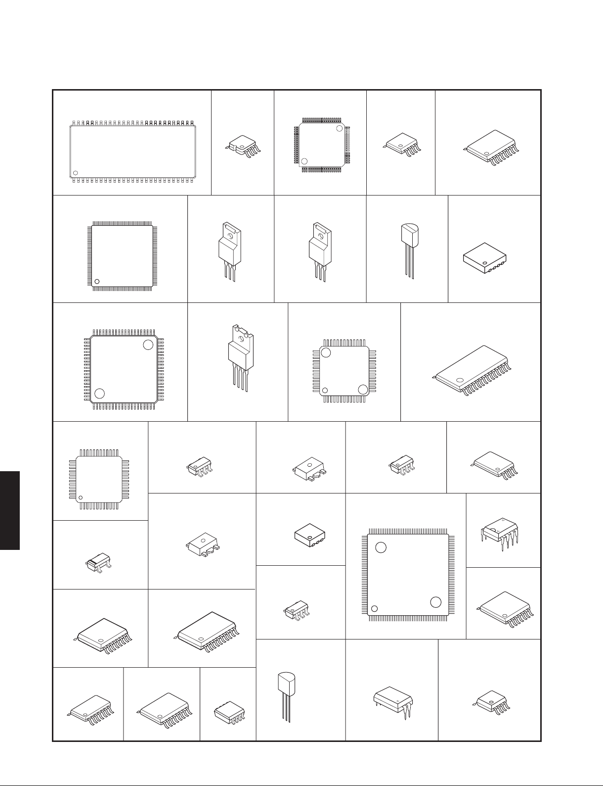
RX-V579/TSR-5790
Cathode
+
1N4003S
RS203M 2.0A 200V
• Diodes
• Transistors
INA6002AC1-TH12-1W
INC6002AC1-T112-1W
1
5
4
HN4B01JE
E
C
B
2N5401C-AT
■ PIN CONNECTION DIAGRAMS
• ICs
A3V64S40GTP-60
D80YK113DPTP400
132
133
176
ML9286-03GAZ0ARL
61
80
1
BA4560F
8245
8
1
721
KIA7805API
89
88
45
441
KIA7812API
IN
COM
OUT
NJM2388F33
4160
40
1
1.
IN
V
2.
21
20
VOUT
3.
GND
4.
ON/OFF CONTROL
4
BD3473KS2
4
61
80
120
KIA7912PI
GND
NJW1329FH3
4160
40
21
OUT
IN
39 27
1
BD9328FJ
8
LM19CIZ/LF
+V
6204
4125
13
4
1
S
OUT
V
GND
PCM1681PWPR
28
BH76360FV-E2
16
MFI337S3959
5
8
1
8
1
4
1
14
PCM9211PTR
36
37
48
1
RP130Q331D-TR-F
RX-V579/TSR-5790
RP130Q501D-TR-F
TC74VHC157FT
16
TC74VHCU04FT
14
R1163N501B-TR-FE
25
24
13
12
3
4
2
1
RP132H331D-T1-FE
4
5
3
3
1
1
5
4
TC74LCX245FT
8
1
TC7MBL3257CFK
8
7
16
1
20
1
TC7WHU04FU
5
6
8
1
1
R1172H121D-T1-F
R1172H501D-T1-F
1
3
4
RP508K101B
4
6
3
1
SN74LVC1G17DCKR
4
5
10
3
1
TL431ACLPR W25Q80DVSSIG
4
1
2
3
1: CATHODE
2: ANODE
3: REF
R3116N271A-TR-F
5
SII9573CTUC
133
176
TLP781
132
4
5
4
3
1
2
1
R1EX25032ATA00I
5
8
STR2A152
89
88
8
TC74VHC125FT
14
45
441
W25Q16DVSSIG
8
4
1
4
1
8
7
1
4
1
82
Page 83
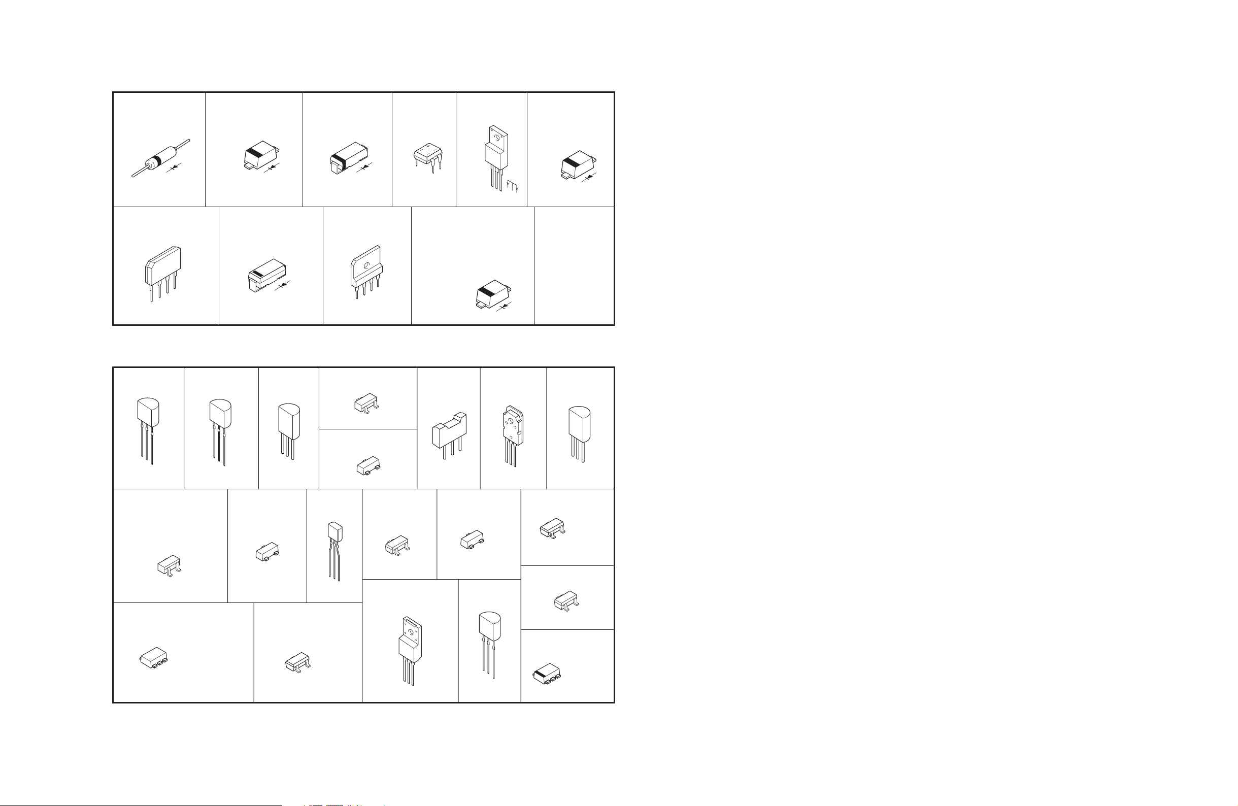
• Diodes
RX-V579/TSR-5790
1N4003S
Cathode
RS203M 2.0A 200V
AC
+
• Transistors
2N5401C-AT
Anode
–
AC
1SS355VM RB215T-90
Anode
Cathode
SARS05
D1FL20U
Anode
Cathode
TS6P03G
DB156
UDZV13B
UDZV3.9B
UDZV4.7B
Anode
UDZV5.1B
UDZV7.5B
UDZV20B
UDZV27B
–
AC
AC
+
Cathode
2SA1708
C
E
B
2SC4488
2N5551C-AT
Cathode
2SA1145 2SA1162-Y(TE85R,F)
1
2
3
Anode
2SA1941
2SC5198
RB500V-40
RB501V-40
RB521S-30
Anode
Cathode
2SC2229
E
C
B
INA6002AC1-TH12-1W
INC6002AC1-T112-1W
C
E
B
HN4B01JE
4
5
3
1
1. BASE 1 (B1)
2. EMITTER (E)
3. BASE 2 (B2)
4. COLLECTOR 2 (C2)
5. COLLECTOR 1 (G2)
B
C
E
E
C
2SC4081UBTLR
C
E
B
KRA104S-RTK
KRC102S-RTK
OUT
B
2SC4115S
COMMON
IN
2SA1576UBTLR
C
B
2SD2704 K
E
C
B
KTA1046-Y-U/PFY KTC3198
KTA1659A
B
C
E
E
DTA044EUBTL2SC2713-GR
B
C
E
DTC114EUA
DTC044EUBTL
C
E
B
3
2
1: IN
1
2: GND
3: OUT
E
C
B
3
1
1: GND
2: IN
2
3: OUT
KTC3875S
C
E
B
RAL035P01
4
E
C
B
C
E
B
6
1. DRAIN
2. DRAIN
3. GATE
3
4. SOURCE
5. DRAIN
1
6. DRAIN
83
Page 84
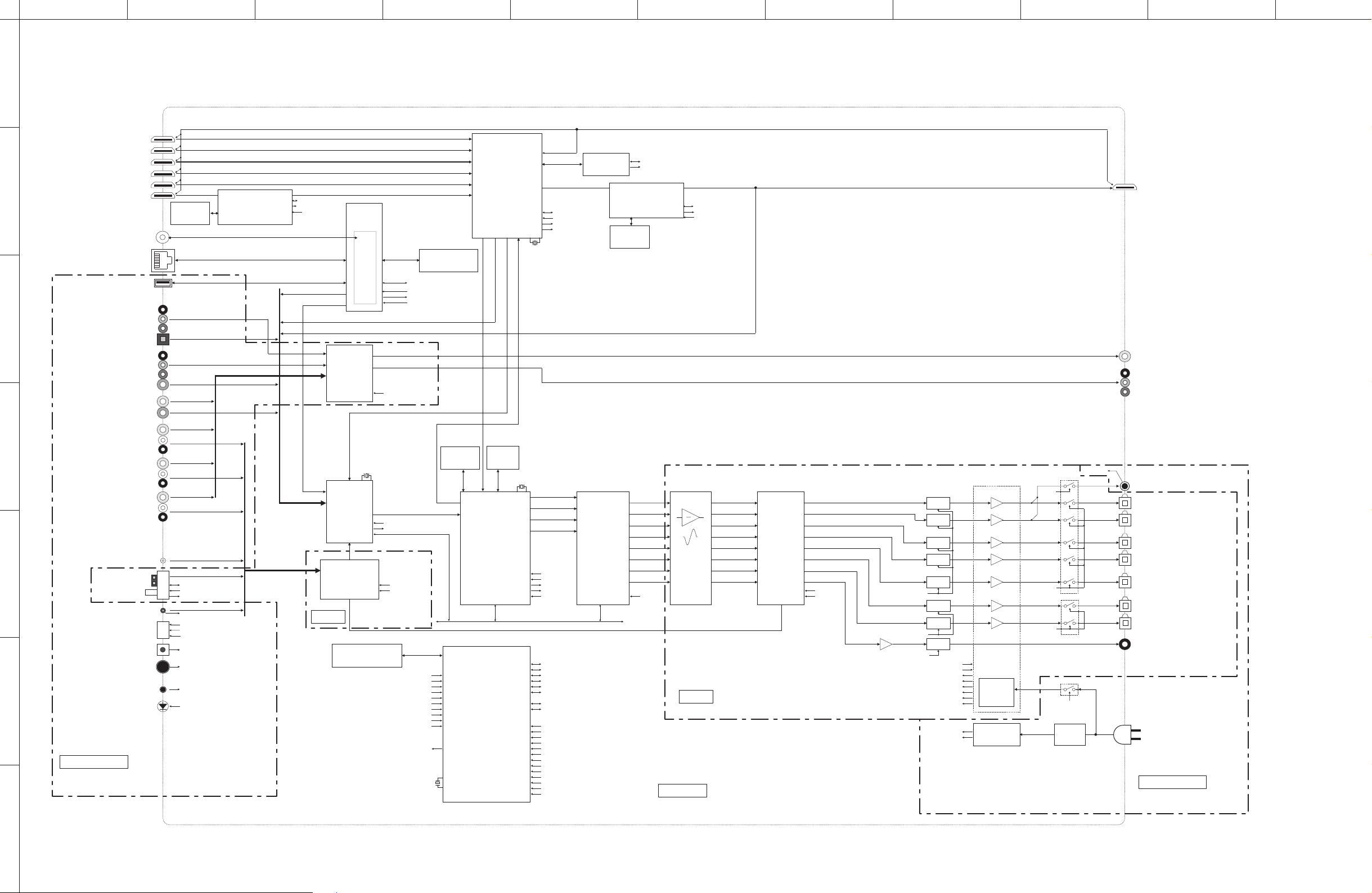
RX-V579/TSR-5790
_
(
)
_
JIHGFEDCBA
1
2
3
4
5
6
■ BLOCK DIAGRAMS
HDMI IN 1
HDMI IN 2
HDMI IN 3
HDMI IN 4
HDMI IN 5
HDMI IN 6
Wireless Antenna
Ethernet
Front USB
AV1
AV2
AV3
AV4
AV5
AV6
AUX
Portable
AM/FM
IC TUNER
TU-04
YPAO MIC In
FL Display
IR Remote Sensor Out
Rotary Encoder
Front Panel Button
Standby LED
OPERATION
・See page 110–111 →
SCHEMATIC DIAGRAM
IC902
FLASH ROM
8Mb
(Component)
(Optical)
(Component)
(Coaxial)
(Composite)
(Coaxial) HDMI_I2S
(Composite)
(Analog)
(Composite)
(Analog)
(Composite) SD0
(Analog)
(Analog) DA_SBL DASBL VOSBL SR SR
(Analog) DSP_N_RST
TUN_SCL/SDA VOL_SCK DSP_N_INT
TUN_N_RST VOL_MOSIDSP_N_RDY VOL_SCK
TUN_N_INT DS P_FMTDAC_N_CS VOL_MOSI
(Analog)
MIC_N_DET
FLD_N_RST
FLD_N_CS
FLD_MOSI/FLD_SCK
REM_IN
VOL_RA <Interrupt>UART0 FL TRANS_RY Amp block
VOL_RB NMIUART1 DSP/DAC/DIR AMP_LMT Heat sink
KEY1
KEY2
PSW_DET
STBY_LED
IC901
HDCP2.2 Receiver
SII9679CNUC
IC1
IN1
HDMI Rx/Tx
SII9573CTUC
IN2
IN3
IN4
IN5
68, 69
HDMI_SCL/HDMI_SDA
20
HDMI_N_INTR HDMI_SCL/HDMI_SDA
34
HDMI_N_RST HDMI_SCL/HDMI_SDAHDMI_N_INTT
NCPU_SPDIF NCPU_SPI_N_CS
NCPU_I2S NCPU_N_RST
HDMI_SPDIF
HDMI_ARC
CB951
Board Connector
To
Network Module
Network
Module
NW-01
IC502
Analog Video
Amp & Selector
NJW1329FH3
XL61
24.576
39
IC61
DIR & ADC
PCM9211PTR
IC203
Selector & E-Vol
BD3473KS2
Apple CoProcessor
14
16
12
18
22
(Composite)
(Component)
VSEL1/VSEL2/CVBS
MHz
40
DIR_I2S DA_FRDAF RVOFR
34
DIR_N_RST DA_SLDASLVOSL
2
DIR_N_INTSD3
10
11
MFI337S3959
NCPU_SPI_MOSI/NCPU_SPI_MISO
/NCPU_SPI_SCK
NCPU_SPI_REQ
ON
AUP_I2S
MAIN
IC22
EEPROM 32kb
R1EX25032ATA00A
10
HDMI_N_INT /INT0UART6 NetCPU I_PRT Main Power Supply
14
DSP_N_INT/INT1 UART10 EEPROM DC_PRT
19
DIR_N_INT /INT2SI/O0 HDMI THM1_PRT
88
PSW_N_DET/INT5 SI/O1TUNER THM2_PRT
101
TUN_N_INT/INT6 SI/O3 THM3_PRT
NCPU_AMUTE /INT8 SSP OSD FLASH AMP_OLVPRY
ACPWER_DET/INTE AIN1 DE ST
29
27
REM_IN /INTBCEC HDMI_CEC
109
MHL_N_INT /INTC
113
HDMI_MUTE/INTD <AD Port>
123
39
AMP_LMTTimerBFou tAIN5THM1_PRT
118
XL21
8.0MHz
120
IN6
IC957
DSD
IC42
FLASH ROM
8Mb
TMPM362F10FG
<Timer>AIN4 KEY3
IC43
SDRAM
64Mb
XL41
20MHz
143
IC41
AUDIO DSP
D80YK113DPTP400
DSP
IC21
CPU
<Serial>
ROM: 1024kB
RAM: 64kB
MOSI/DSP_MISO/DSP_SCK
HDMI_CEC
72
66, 67
69
HDMI_N_RST HDMI_N_RST
68
HDMI_N_INT
129
HDMI_MUTE
113
114
XL1
27.0
MHz
145
SD1
SD2 FR
146
8
DSP_N_CS DA_SW DASW VOSW CC
21
7
23
IC2
FLASH ROM
16Mb
FLASH ROM
IC62
AUDIO DAC
PCM1681PWPR
5, 2, 6
OSD_MOSI/OSD_MISO/OSD_CLK
OSD_N_CS
1
IC904
HDCP2.2 Transmitter
SII9678CNUC
IC903
68, 69
20
34
8Mb
27 63
DA_FLDAFLVOFL FL
26
20
19
DA_SRDASRVOSR
22
DA_C DACVOC
16
15
DA_SBR DASBR VO SBR
21
2
IC221,222,223,224
A-Filter
MAIN
132
133
AIN2 KEY1 CPU_N_RST
134
AIN3 KEY2 ACPWR_DET
135
136
137
AIN6 THM2_PRT
138
AIN7 PS1_PRT
139
AIN8 PS2_PRT
140
AIN9 PS3_PRT
141
AIN10DC_PRT
142
AIN11AMP _OLV
143
AIN12USB_VBUS_PRT
AIN13+5EX_PRT
DIGITAL
IC203
Selector &
E-Vol
62
BD3473KS2
65
64
67
69
68
66
・See page 112–114 →
SCHEMATIC DIAGRAM
・See page 103–109 →
SCHEMATIC DIAGRAM
HDMI Out
Monitor Out
Monitor Out
HP_N_DET
Speaker Relay
FI541
LINE
FILTER
RY221
7
8
5
6
3
1
2
4
10
11
IC202
MUTE_5CH
MUTE_SB
MUTE_SW
MUTE
MUTE
MUTE
MUTE
MUTE
MUTE
MUTE
MUTE
SL SL
SBL SBL
SBR SBR
SW PREOUT
Main Power
Supply
(Main
Trans)
AC-DC
Power Supply
FL
FR
SPRY_5CH
SPRY_SB
HPRY
Head Phone
Front L
Surround L
Surround R
Center
Surround Back
/Bi AMP L
Surround Back
/Bi AMP R
Sub Woofer
AC In
OPERATION
・See page 110–111 →
SCHEMATIC DIAGRAM
7
84
Page 85
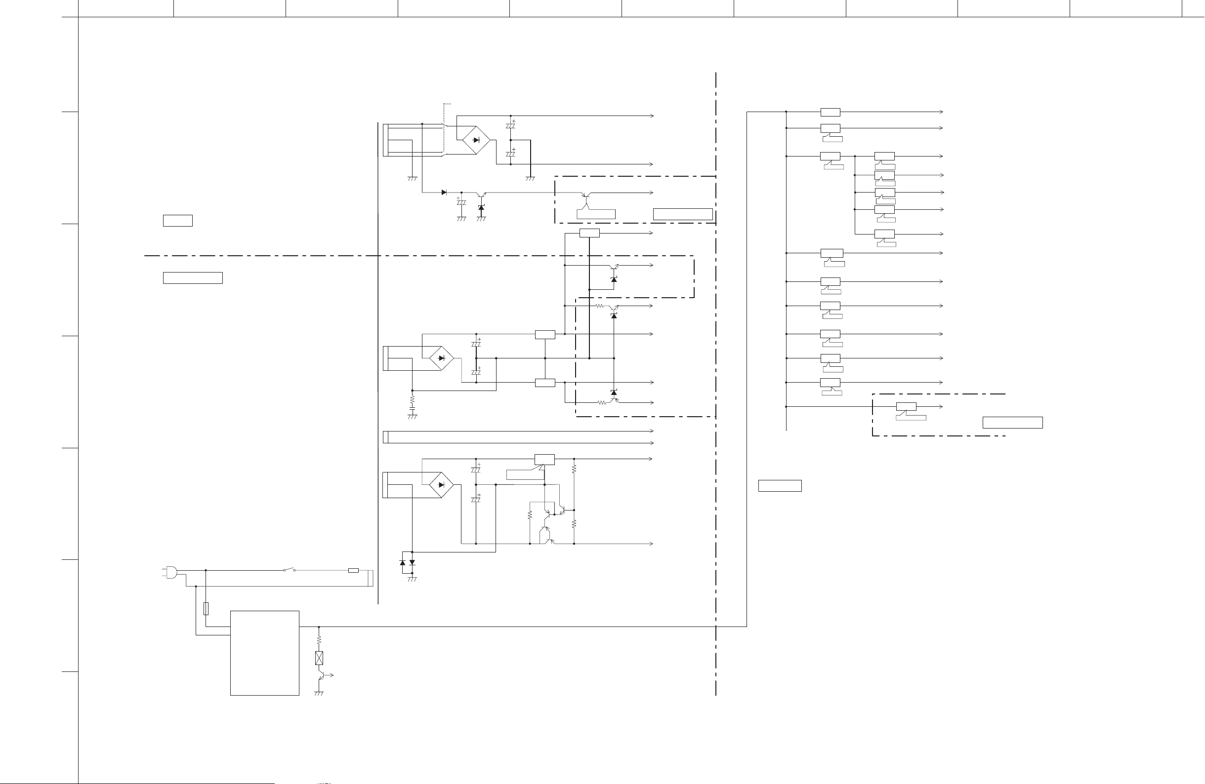
JIHGFEDCBA
1
2
3
4
5
6
7
RX-V579/TSR-5790
Speaker Impedance relay
RY226
RY226
D2146C2185 +3.3Scontrol circuits around CPU
D2147
MAIN
OPERATION
・See page 112–114 →
SCHEMATIC DIAGRAM
・See page 110–111 →
SCHEMATIC DIAGRAM
C2194
D5205
Q2186
C5219
C5220
D2144
D2150
D5203
C5217
C5218
Power Supply Section Block Diagram
+B Power AMP
C2186 +3.3HHDMI (IC1,901,904)
+39V
㼂㻵㻰㼋㻼㻻㻺㻌
㻔㻲㼞㼛㼙㻌㻼㻯㻮㻌㻰㻵㻳㻵㼀㻭㻸㻕㻌
IC523
㻗㻝㻞㼂㻌
㻙㻝㻞㼂㻌
IC524
IC522
㻗㻟㻚㻟㼂㻌
OPE
OPE
Q4007
㻲㻸㼋㻼㻻㻺
㻌
㻔㻲㼞㼛㼙㻌㻼㻯㻮㻌㻰㻵㻳㻵㼀㻭㻸㻕
IC271
㻗㻡㻭
MAIN Apple Coprocessor(IC954)
Q5201
D5201
Q2001
D2001
D2002
Q2002
-B Power AMP
+
FL Driver +1HT HDMI (I C904)
OPERATION
+5ADAC/ADC
+3.3TTuner
+7AVolume +5NET WiFi-Module
+12A
-12A
-7A
F1 FL filament
F2 FL filament
+3.3VAnalog VIDEO
+5.5V
DIGITAL
IC91
㻗㻟㻚㻟㻹㻌
IC89
㻗㻟㻚㻟㻿㻌
㻗㻟㻚㻟㻿㼋㻼㻻
IC83
㻗㻟㻚㻟㻰㻌
㻰㻯㻰㻯㼋㻼㻻
IC82
㻮㻰㻥㻟㻞㻥㻱㻲㻶㻌
㻴㻰㻹㻵㼋㻼㻻㻺㻌
IC86
㻗㻝㻚㻞㻰㻌
㻰㻿㻼㼋㻼㻻㻺
IC90
㻗㻡㻺㻱㼀㻌
㻺㻯㻼㼁㼋㻼㻻
IC84
㻗㻡㻴㼀㻌
㻴㻰㻹㻵㼋㻼㻻㻺
IC85
㻗㻡㻴㻌
㻴㻰㻹㻵㼋㻼㻻㻺
IC81
㻗㻡㻰㻌
㻰㻿㻼㼋㻼㻻㻺
・See page 103–109 →
SCHEMATIC DIAGRAM
Q804
㻗㻟㻚㻟㻴㻌
㻴㻰㻹㻵㼋㻼㻻㻺
㻗㻝㻴㻾㻌
㻴㻰㻹㻵㼋㻼㻻㻺
㻗㻝㻴㼀㻌
㻴㻰㻹㻵㼋㻼㻻㻺
㻗㻟㻚㻟㻰㻿㻼㻌
㻰㻿㻼㼋㻼㻻㻺㻌
Q806
㻗㻟㻚㻟㻺㻌
㻺㻯㻼㼁㼋㻼㻻
IC87
IC88
Q805
IC402
㻗㻡㼁㻌
㼁㻿㻮㼋㼂㻮㼁㻿㼋㻼㻻㻺
+3.3MCPU(IC21)/Standby LED/ Remote/key input
+1HR HDMI (IC901)
+3.3DSPDSP(IC41), SDRAM(IC43), FLASH ROM(IC42)
+3.3N WiFi-Module
+1.3HHDMI(IC1)
+1.2DSPDSP(IC41)
+5H䠰
+5HHDMI(IC1)
+5D
+5U
DIR(IC61), DAC(IC62), FL Driver
HDMIout connector(+5VPower)
PCB MAINOptical In ( 25mA x 2) Coax In、 Buffer
iPod/USB㟁※
OPERATION
Q5204
RY541F5402
F5401
-3.3VAnalog VIDEO
㻭㻯㻛㻰㻯㻌㻯㼛㼚㼢㼑㼞㼠㼑㼞㻌
RY541
PRY
Q5401
85
Page 86
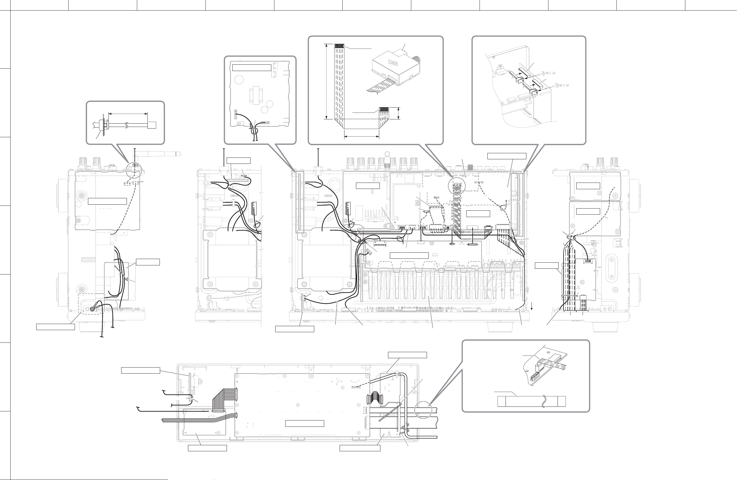
RX-V579/TSR-5790
JIHGFEDCBA
1
■ WIRING DIAGRAMS
to AM/FM TUNER
Contact side
AM/FMTUNER
• OVERALL ASSEMBLY
MAIN (3) (CB271)
OPERATION (2)
PN251
MAIN (2) (CB251)
Side view
to DIGITAL
(CB953)
to DIGITAL
(CB21)
MAIN (5)
MAIN (3)
MAIN (2)
PN251
CB352
to MAIN (1)
(W2001)
DIGITAL
(3/4")
95 mm
2
Side view
Power cable
Cord Stopper
80 mm
(3-1/8")
to OPERATION (2)
(CB541)
W5402
to DIGITAL
(CB27)
PN541
W5401
to DIGITAL (CB81)
Top view Top view
R, Vmodels
MAIN (4)
CB301
Contact side
15 mm
(5/8")
3
CB544
CB541
OPERATION (2)
CB222 CB222
PN221
PN221
4
MAIN (6)
POWER
TRANSFORMER
POWER
TRANSFORMER
to DIGITAL
(CB26)
MAIN (1)
to OPERATION (2)
(W5402)
PN481
CB524
PN521
CB525
20 mm
(7/8")
(OPERATION (3))
(MAIN (1))
CB223
CB81CB27 CB81
CB522
to OPERATION (2) (W5401)
PN522
(MAIN (1))
CB221
CB27
OPERATION (4)
CB953
W5001
CB22
W4004
CB23
CB523
AM/FM
TUNER
(OPERATION (3))
CB505
DIGITAL
CB25
CB521
(OPERATION (3))
W2001
(CB62)
DIGITAL
(CB63)
OPERATION (3)
PN501
CB26 CB21
PN371
CB477
View A
PN352
CB351
5
CB402 CB405
OPERATION (7)
to OPERATION (7) (W4761)
to OPERATION (5)
(W4501)
OPERATION (7)
to MAIN (1)
(W2111)
Front panel (View A)
OPERATION (7)
6
to chassis
to chassis
to OPERATION (4)
to MAIN (1)
(CB525)
W4761
(W2111)
7
CB477
CB451
W4501
OPERATION (5)
CB401
CB403
OPERATION (1)
OPERATION (10)
to OPERATION (1) (CB403)
W4004
CB404
CB405
CB402
OPERATION (6)
CB471
PN471
AMP UNIT
PN472
to MAIN (5)
(CB351)
toDIGITAL
(CB21)
toDIGITAL
(CB953)
Flexible flat cable
Plain side
to OPERATION (1)
(CB405)
to OPERATION (1)
(W4004)
Fold
to MAIN (5)
(CB351)
86
Page 87
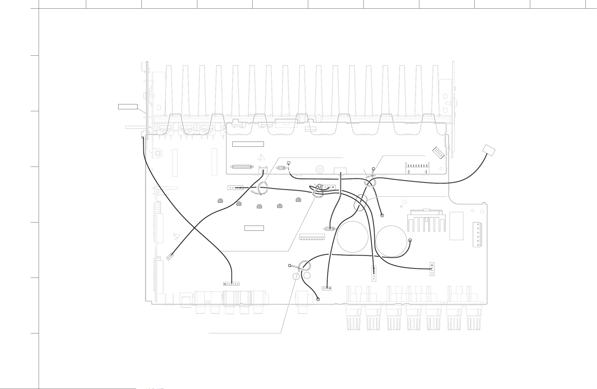
JIHGFEDCBA
1
2
3
4
5
6
7
RX-V579/TSR-5790
• AMP UNIT
MAIN (5)
CB352
W2002
OPERATION (4)
CB521
W2102A
Q2121
Q2119
Fix the wires by style-pin (PN222) not to
approach Q2117/2118/2119/2120/2121,
and not to touch with the W2101.
CB526
PN224
Q2120
MAIN (1)
Fix the wires by style-pin (PN224) not to
approach Q2117/2128/2119/2120/2121,
and keep the wire close to the edge
of OPERATION (4).
CB523
PN222
Q2118
Q2117
CB221
PN223
C2030
W2103A
CB223
C2029
CB522
C2185
W2104
CB525
Fix the wires by PN522.
CB524
PN522
Check whether W2111 is passing under
2 wires as shown in the figure.
W2101
HS221
C2186
W2103B
W2102B
OPRATION (7)
(CB477)
CB222
W2001
W2111
Fix the wires by style-pin (PN223)
and push it down not to float from PCB.
87
Page 88
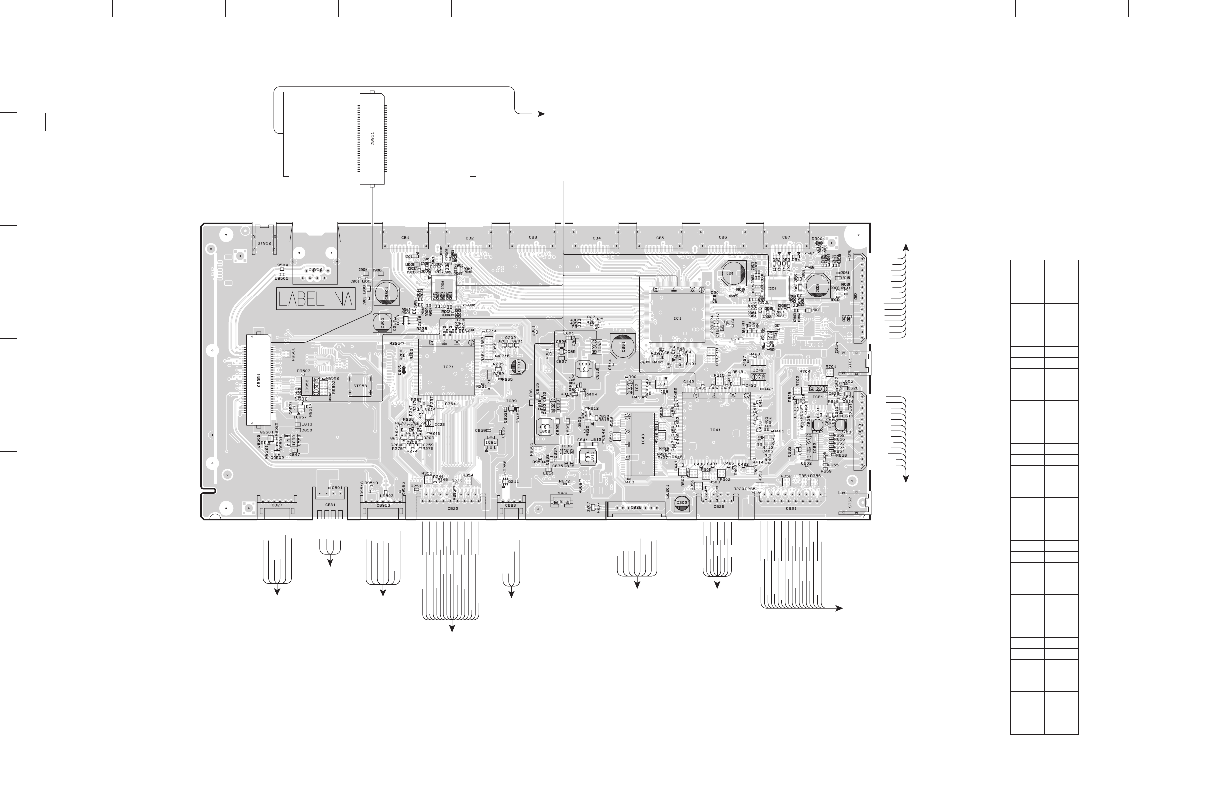
RX-V579/TSR-5790
JIHGFEDCBA
1
2
3
4
5
6
■ PRINTED CIRCUIT BOARDS
DIGITAL
(Side A)
ETH_RX_M
ETH_TX_M
DGND
NCPU_SPI_MOSI
NCPU_SPI_N_CS
NCPU_N_RST
NCPU_MUTE1
NCPU_TXD
NCPU_N_INT
NCPU_ADT_MUTE
NCPU_VBUSDRV
USB_DM
USB_DP
DGND
+5WLAN
NETWORK
IC957
CB27
PRY
DEST
DGND
CPU_N_RST
ACPWR_DET
11
IC90
CB951
+3.3M
OPERATION (2)
(W5402)
ETH_RX_P
ETH_TX_P
NCPU_SPI_SCK
NCPU_SPI_MISO
DGND
NCPU_MUTE0
NCPU_RXD
DGND
DBG_UART_TXD
NCPU_PHOLD
USB_VBUS
USB_DM
USB_DP
DGND
+5WLAN
(NET)
CB952
10
IC958
120
5418
4513
CB81
+5.5V
+5.5V
DGND
DGND
OPERATION (2)
(W5401)
DGND
NCPU_ADT_MCKR
DGND
NCPU_ADT_SDR0
NCPU_ADT_WCKR
NCPU_ADT_BCKR
DGND
NCPU_Z_AUP_MCKX
DGND
NCPU_Z_AUP_BCKX
NCPU_Z_AUP_WCKX
NCPU_Z_AUP_SDX0
DGND
NCPU_AUP_MCKX
DGND
NCPU_AUP_BCKX
NCPU_AUP_WCKX
NCPU_AUP_SDX0
NCPU_AUP_SDX3
NCPU_AUP_SDX2
NCPU_AUP_SDX1
DGND
AP_SCL
AP_SDA
+3.3VMMC
DBG_UART_RXD
DGND
DGND
+5NET
+5NET
HDMI 6
HDCP2.2
CB1CB2 CB3CB4 CB5CB6 CB7
IC23
CB953
DGND
Vreturn
-DATA
+DATA
FG
USB_VBUS_PON
+5.5V
OPERATION (1)
(W4004)
76
1
19
20
1345
36
37
72
73
58
IC22
14
MUTE_SW
MUTE_5ch
THM2_PRT
MUTE_SB/MUTE_Z2
MAIN (1)
Network Module
ネットワークモジュール
No replacement part available.
サービス部品供給なし
HDMI 5 HDMI 4 HDMI 3 HDMI 2 HDMI 1
58
57
IC901
39
38
IC21
CB22
DC_PRT
VOL_SCK
AMP_OLV
I_PRT
DGND
AMP_LMT
VOL_MOSI
(CB221)
1
144
109
108
54
IC91
13
HPRY
SPRY_5CH
TRANS_RY
HP_N_DET
PS1_PRT/PDSW
OPERATION (3)
SPRY_SB/SPRY_B
IC89
3
142
CB23
DGND
CVBS_ON
AVID_SCL/VSEL1
AVID_SDA/VSEL2
(W5001)
4
1
IC85
2
3
148
IC83
5
5
IC86
184
CB29
(for factory)
8
IC82
415
OPERATION (4)
45
88
89 132
8
IC2
415
1
IC43
27 28
+3.3T
VID_PON
PS1_PRT
PS2_PRT
THM1_PRT
R_200_DET
(CB521)
IC3
54
+3.3S
DGND
IC1
18
169
45
88
89 132
AM/FM TUNER
(BD/DVD)
144
176
133
IC41
SDA
+3.3T
N_INT
NC
SCL
N_RST
Rch
GND
Lch
58
761920
1
18
45
85
IC42
14
144
176
133
FL_PON
HDMI OUT
HDCP2.2
3957
38
IC904
IC4
CB21CB26CB25
KEY1
REM_IN
FLD_SCK
MIC_N_DET
FLD_N_RST
KEY2
FLD_MOSI
FLD_N_CS
PSW_N_DET
13
IC61
24
11428
VOL_RA
VOL_RB
+3.3M
DGND
+3.3DSP
112
48
37
3625
IC62
15
IN_RC
IN_RD
STBY_LED
MAIN (3)
(CB271)
+3.3DSP
AV1_D
DGND
AV2_D
DGND
AV3_D
AUD_DET
AGND
CB62
+5A
TUL
TUE
TUR
NETR
NETE
NETL
ADR
ADL
DA-FR
AGND
DA-FL
DA-SR
AGND
CB63
DA-SL
DA-SW
AGND
DA-C
DA-SBR
DA-SBL
MAIN (2)
(CB251)
OPERATION (1)
(CB402)
• Semiconductor Location
Ref no. Location
D52 G3
D53 G3
D54 H3
D205 C4
D9001 H3
IC1 F3
IC2 E4
IC3 F4
IC4 G3
IC21 D4
IC22 D4
IC23 D3
IC41 G4
IC42 G4
IC43 F3
IC61 H4
IC62 F4
IC82 F4
IC83 E4
IC85 E4
IC86 E4
IC89 E4
IC90 C4
IC91 E4
IC901 D3
IC904 G3
IC957 C4
IC958 C4
Q201 E4
Q202 E4
Q203 E4
Q205 E4
Q207 F5
Q208 D4
Q209 D4
Q210 D4
Q211 E5
Q801 F4
Q802 F4
Q804 F4
Q805 F4
Q9501 C4
7
Q9502 C5
88
Page 89
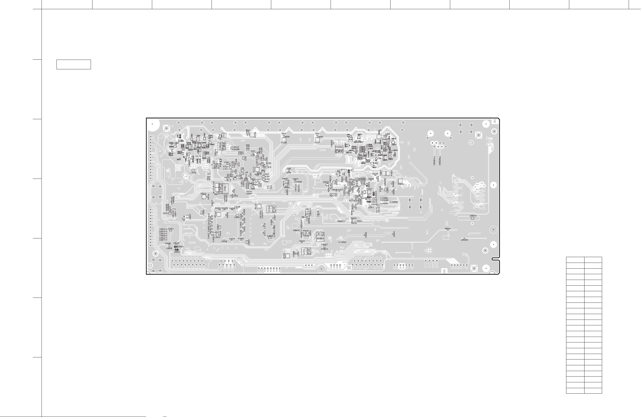
JIHGFEDCBA
1
2
3
4
5
6
7
RX-V579/TSR-5790
DIGITAL
(Side B)
IC84
3
4
5
1
6
1
4
3
IC88
5
IC903
8
120
10
4
1
IC9
11
6
7
IC44
1
13
8
IC902
451
4
6
IC87
3
1
IC27
3
4
5
1
8
IC953
1619
7
8
IC71
1
14
• Semiconductor Location
Ref no. Location
D2 F3
D24 C3
D201 F4
D202 F4
D203 F4
D204 F4
D601 C5
D602 C5
IC9 D4
IC27 F4
IC44 D4
IC71 E5
IC84 C3
IC87 F3
IC88 C3
IC902 F3
IC903 D3
IC953 E4
Q3 F3
Q204 F4
Q206 E4
Q9001 F3
Q9002 F3
89
Page 90
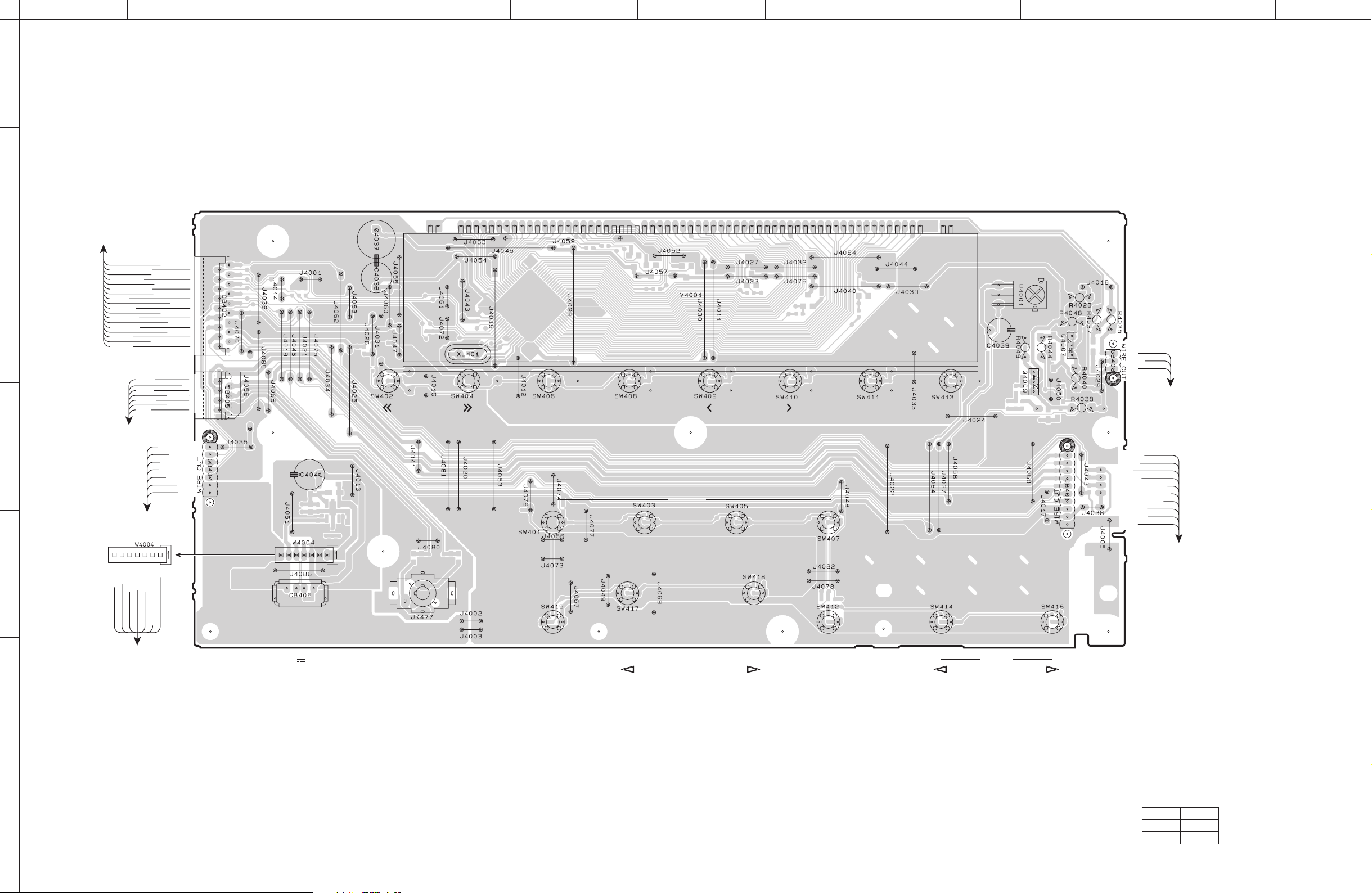
JIHGFEDCBA
RX-V579/TSR-5790
1
OPERATION (1)
(Side A)
2
DIGITAL (CB21)
+12A
-12A
AUXL
MIC
(CB471)
-DATA
Vreturn
FL_PON
FLD_N_CS
FLD_MOSI
PSW_N_DET
KEY2
+3.3DSP
DGND
+3.3M
STBY_LED
AUXR
AUXE
+3.3DSP
KEY2
VOL_RB
VOL_RA
DGND
FG
+DATA
FG
FG
Remote control sensor
CB402
CB403
F2
+40F
F1
CB404
CB405
W4004
CB406
RADIO
FMAMTUNING
PRESET
SCENE
NET TV BD
MEMORY INFO (WPS)
DVD
CB401
OPERATION (4)
(CB525)
+12A
MIC
E
-12A
MIC_N_DET
PSW_N_DET
STBY_LED
+3.3M
DGND
FG
OPERATION (5)
(CB451)
E
FLD_N_RST
FLD_SCK
MIC_N_DET
KEY1
REM_IN
3
4
VOL_RB
VOL_RA
IN_RD
IN_RC
MAIN (5)
(CB351)
OPERATION (6)
5
GND
+5.5V
USB_VBUS_PON
DIGITAL
(CB953)
5V 1A
(Front USB)
AUX
AUDIO
STRAIGHT
(CONNECT)
PROGRAMTONE CONTROL INPUT
6
• Semiconductor Location
Ref no. Location
7
Q4007 I3
Q4009 I3
90
Page 91
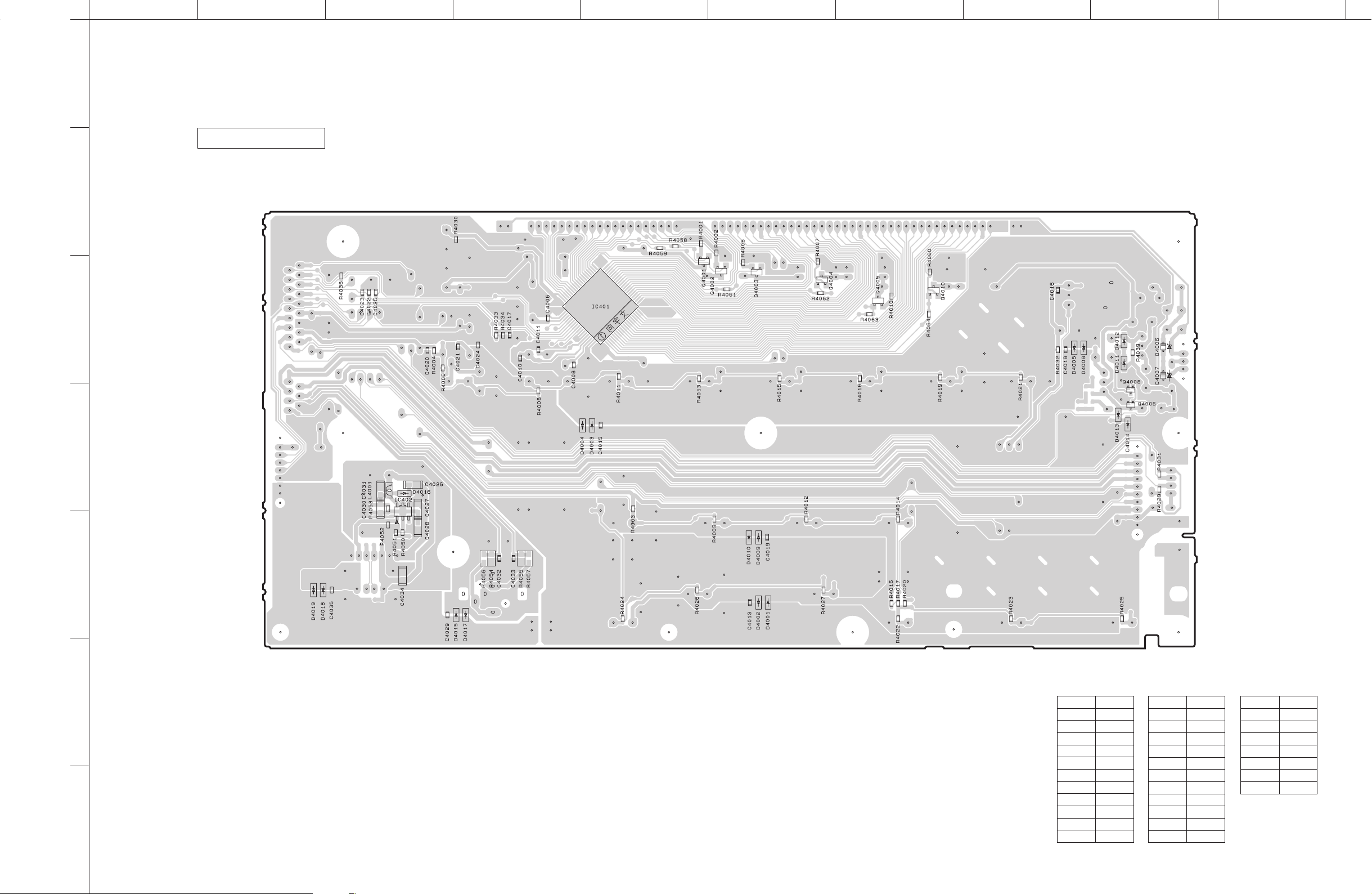
JIHGFEDCBA
1
2
3
4
5
6
7
RX-V579/TSR-5790
OPERATION (1)
(Side B)
41
40
60
IC401
61
80
21
20
1
IC402
5
4
1
3
• Semiconductor Location
Ref no. Location
D4001 F5
D4002 F5
D4003 E4
D4004 E4
D4005 H3
D4006 I3
D4007 I3
D4008 H3
D4009 F5
D4010 F5
D4011 I3
Ref no. Location
D4012 I3
D4013 I4
D4014 I4
D4015 D5
D4016 C4
D4017 D5
D4018 B5
D4019 B5
IC401 E3
IC402 C4
Q4001 E3
Ref no. Location
Q4002 F3
Q4003 F3
Q4004 F3
Q4005 G3
Q4006 I4
Q4008 I4
Q4010 G3
91
Page 92
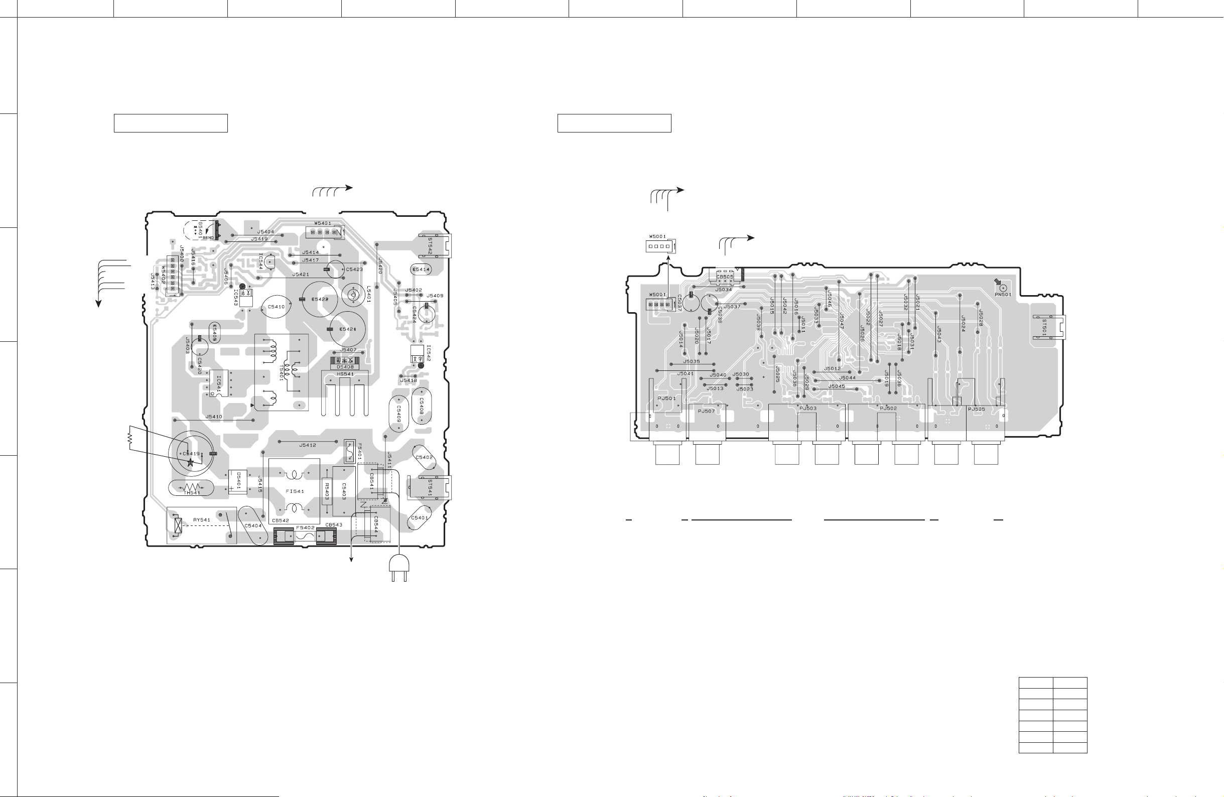
JIHGFEDCBA
RX-V579/TSR-5790
1
OPERATION (2)
(Side A)
OPERATION (3)
(Side A)
2
DIGITAL (CB81)
5.5V
5.5V
GND
GND
W5401
A
5
8
1
IC543
4
IC544
R
K
2
3
3
4
IC542
1
2
DEST
CPU_N_RST
ACPWR_DET
3
DGND
+3.3M
PRY
W5402
DIGITAL (CB27)
4
IC541
4
1
VID_SCL
W5001
DGND
CVBS_ON
VID_SDA
DIGITAL (CB23)
-3.3V
VE
CB505
OPERATION (4)
+3.3V
(CB523)
5 k-ohms
10 W
CB541
5
CB542
CB543
CB544
PR/PB/Y PR/PB/Y PR/PB/Y
MONITOR
OUT
COMPONENT
VIDEO
MONITOR
OUT
AV 6AV 5AV 4AV 3AV 2AV 1
VIDEO
COMPONENT
VIDEO
POWER TRANSFORMER
AC IN
6
7
Safety measures
• Some internal parts in this product contain high voltages and are dangerous. Be sure to take safety measures during
servicing, such as wearing insulating gloves.
• Note that the capacitors indicated below are dangerous even after the power is turned off because an electric charge
remains and a high voltage continues to exist there. Before starting any repair work, connect a discharging resistor
(5 k-ohms/10 W) to the terminals of each capacitor indicated below to discharge electricity. The time required for
discharging is about 30 seconds per each.
C5407 on OPERA
安全対策
・ この製品の内部には高電圧部分があり危険です。修理の際は、絶縁性の手袋を使用するなどの安全対策を行ってください。
・ 下記のコンデンサには電源を OFF にした後も電荷が残り、高電圧が維持されており危険です。修理作業前に放電用抵抗
(5 k Ω /10 W)を下記の各コンデンサの端子間に接続して放電してください。放電所用時間は各々約 30 秒間です。
OPERATION(2)P.C.B. の C5407
TION (2) P.C.B.
• Semiconductor Location
Ref no. Location
D5401 C5
D5408 C4
IC541 B4
IC542 D4
IC543 C3
IC544 C3
92
Page 93
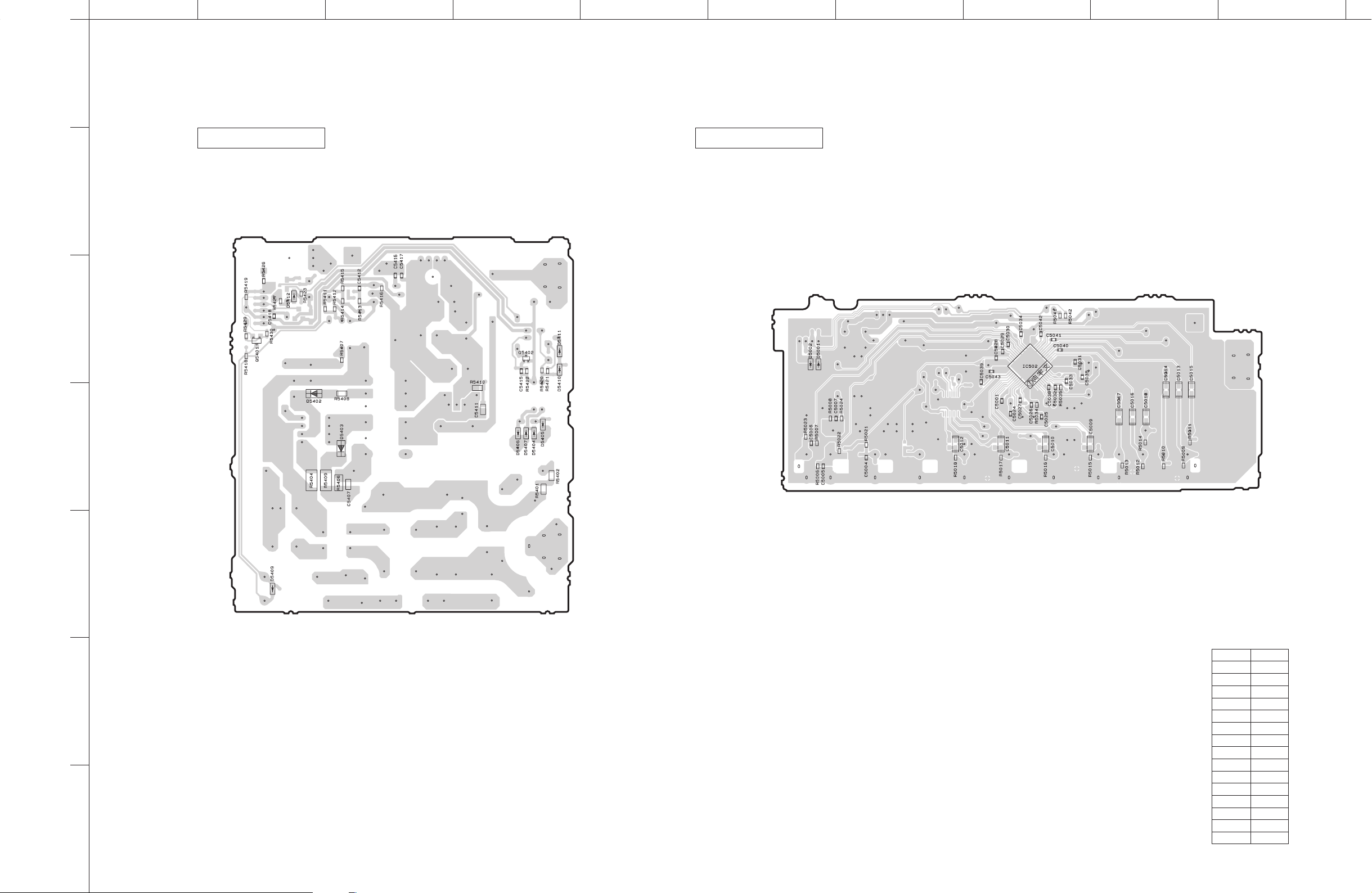
JIHGFEDCBA
1
2
3
4
5
6
7
RX-V579/TSR-5790
OPERATION (2)
(Side B)
OPERATION (3)
(Side B)
27
26
39
40
IC502
52
14
13
1
• Semiconductor Location
Ref no. Location
D5001 F3
D5002 F3
D5402 B4
D5403 C4
D5404 D4
D5405 D4
D5406 D4
D5407 D4
D5409 B5
D5410 D3
D5411 D3
D5412 B3
IC502 H3
Q5401 B3
Q5402 D3
93
Page 94
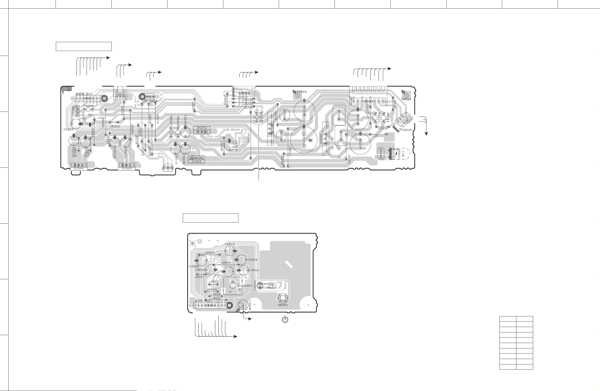
JIHGFEDCBA
RX-V579/TSR-5790
1
OPERATION (4)
2
3
+3.3S
DGND
THM1_PRT
+3.3T
VID_PON
PS1_PRT
PS2_PRT
CB521
COM
OUT
IN
IC524 IC523
(Side A)
DIGITAL
R_200_DET
+12A
CB526
IN
(CB25)
MAIN (1) (W2002)
-12A
AGND
COM
OUT
+3.3VVE-3.3V
CB523
OPERATION (3) (CB505)
VCC
IC521
GND
OUT
MAIN (1) (CB223)
+12A
-12A
+40F
AG2
CB522
1
4
IC522
R, V, S models
AC_12
E_12
AC_12
AC_VVEAC_VF1F2
CB524
POWER TRANSFORMER
F2
+40F
F1
CB525
OPERATION (1)
(CB403)
4
OPERATION (5)
(Side A)
5
POWER
indicator
YPAO MIC
FG
+3.3M
DGND
CB451
-12A
STBY_LED
MIC_N_DET
PSW_N_DET
W4501
E
MIC
+12A
to chassis
(Power)
• Semiconductor Location
Ref no. Location
D4504 E6
D5205 E3
OPERATION (1) (CB401)
D5203 F3
IC521 D3
IC522 D3
IC523 C3
IC524 B3
Q5201 B2
Q5204 D3
6
7
94
Page 95
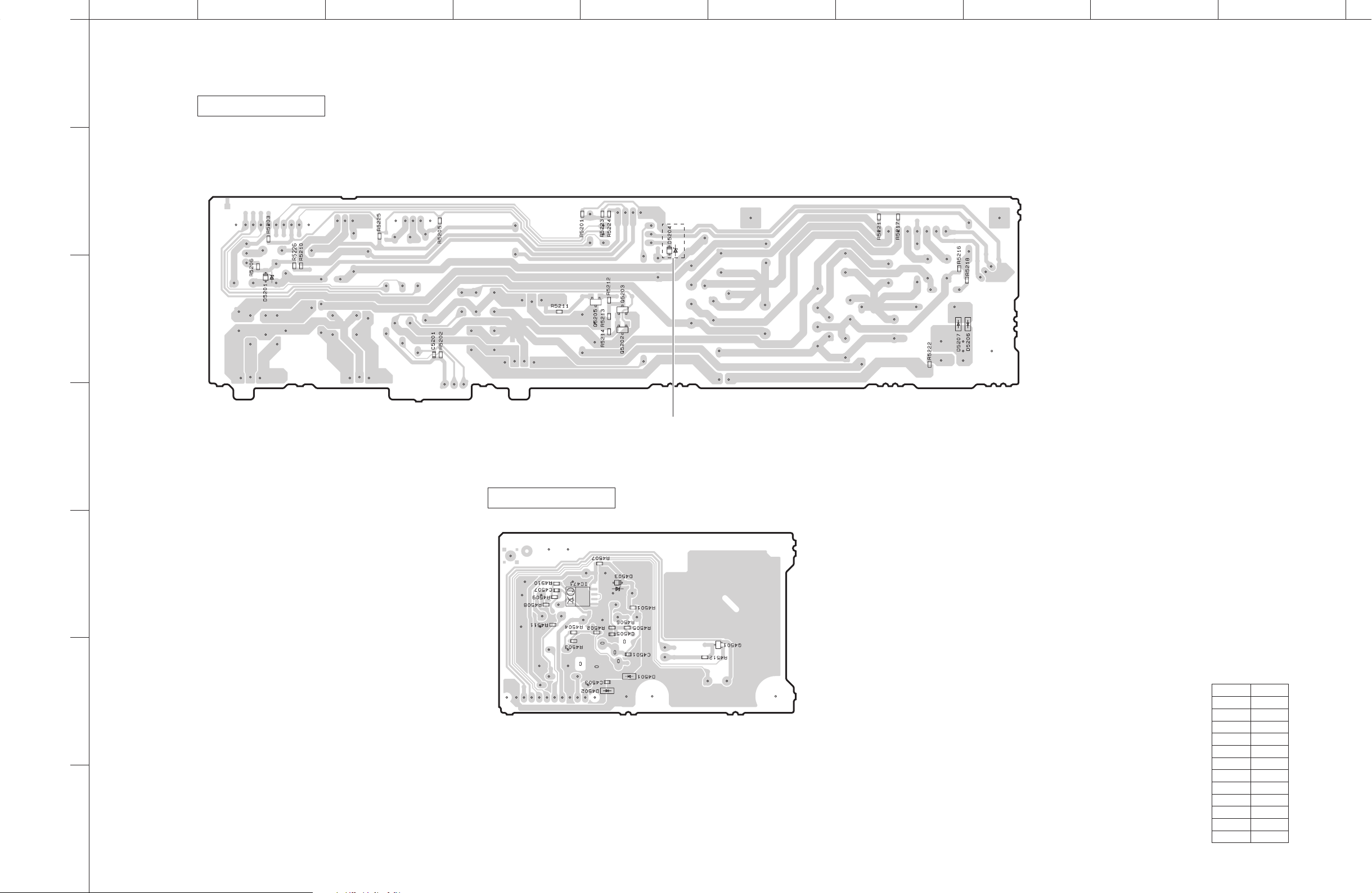
JIHGFEDCBA
1
2
3
4
5
6
7
RX-V579/TSR-5790
OPERATION (4)
(Side B)
R, V, S models
OPERATION (5)
IC471
1
4
(Side B)
8
5
• Semiconductor Location
Ref no. Location
D4501 E6
D4502 E6
D4503 E5
D5201 B3
D5204 E2
D5206 H3
D5207 G3
IC471 D5
Q4501 F6
Q5202 E3
Q5203 E3
Q5205 E3
95
Page 96
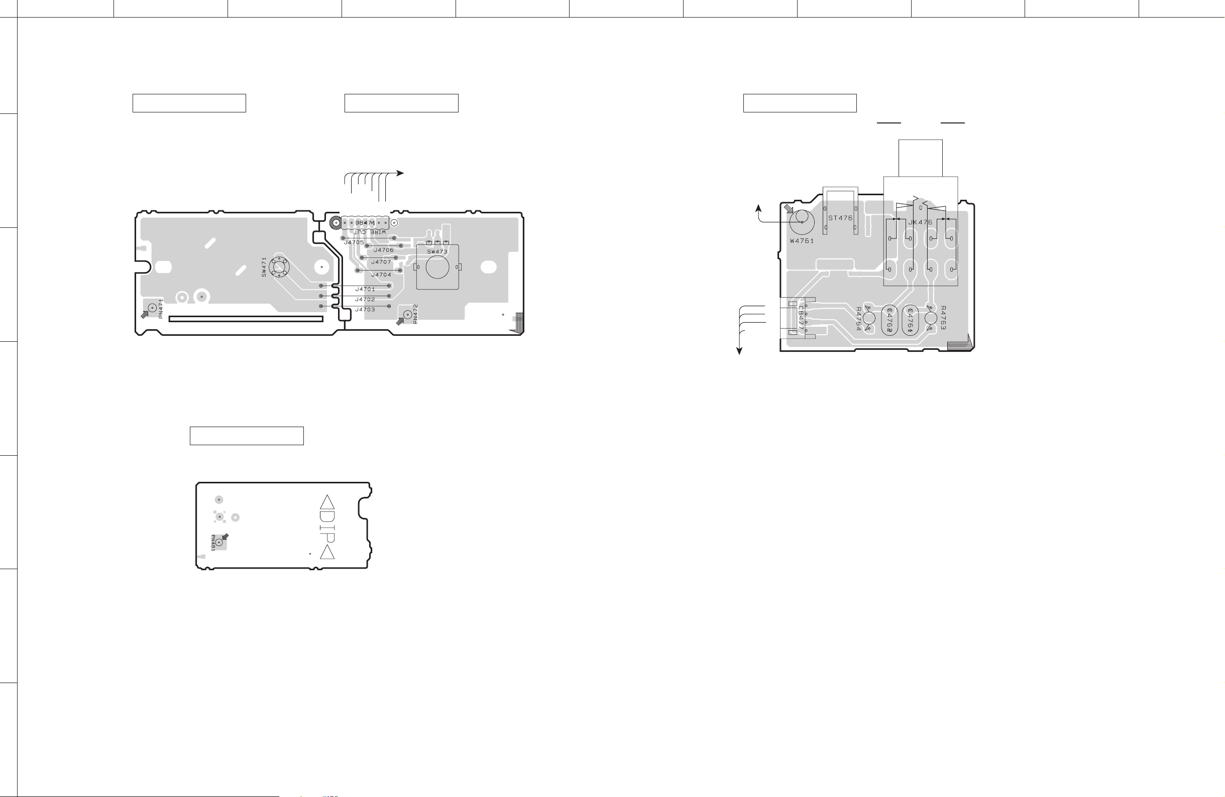
JIHGFEDCBA
RX-V579/TSR-5790
1
OPERATION (10)
(Side A)
2
OPERATION (6)
OPERATION (1)
(CB404)
+3.3DSP
KEY2
VOL_RB
VOL_RA
DGNDFGFG
CB471
(Side A)
OPERATION (7)
to chassis
(Side A)
PHONES
SILENT CINEMA
3
VOLUME
MAIN (1)
(W2111)
HPR
HPE
HPL
HP_N_DET
CB477
4
OPERATION (8)
(Side A)
5
6
7
96
Page 97
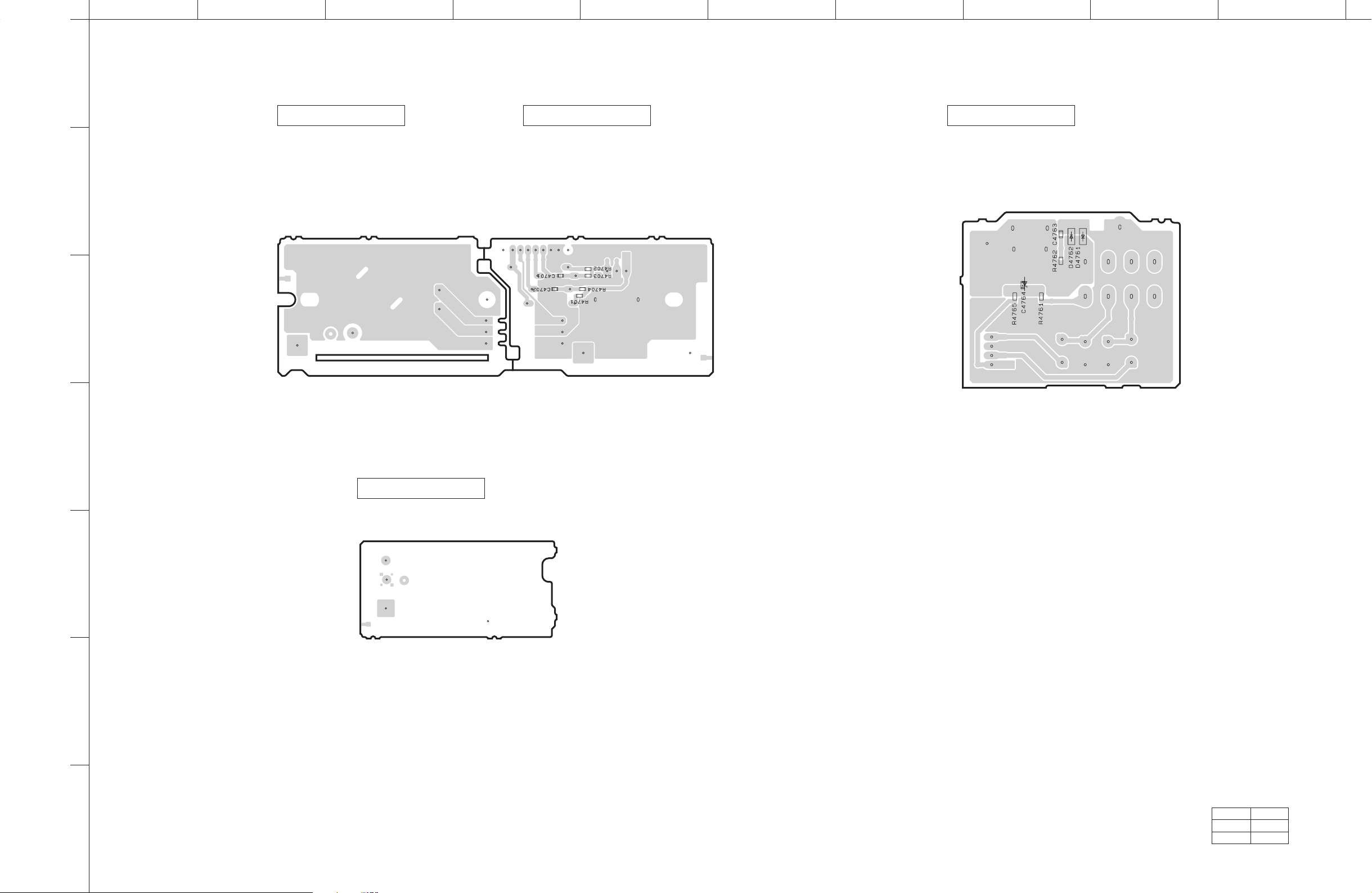
JIHGFEDCBA
1
2
3
4
5
6
7
RX-V579/TSR-5790
OPERATION (10)
(Side B)
OPERATION (6)
(Side B)
OPERATION (7)
(Side B)
OPERATION (8)
(Side B)
• Semiconductor Location
Ref no. Location
D4761 H2
D4762 H2
97
Page 98
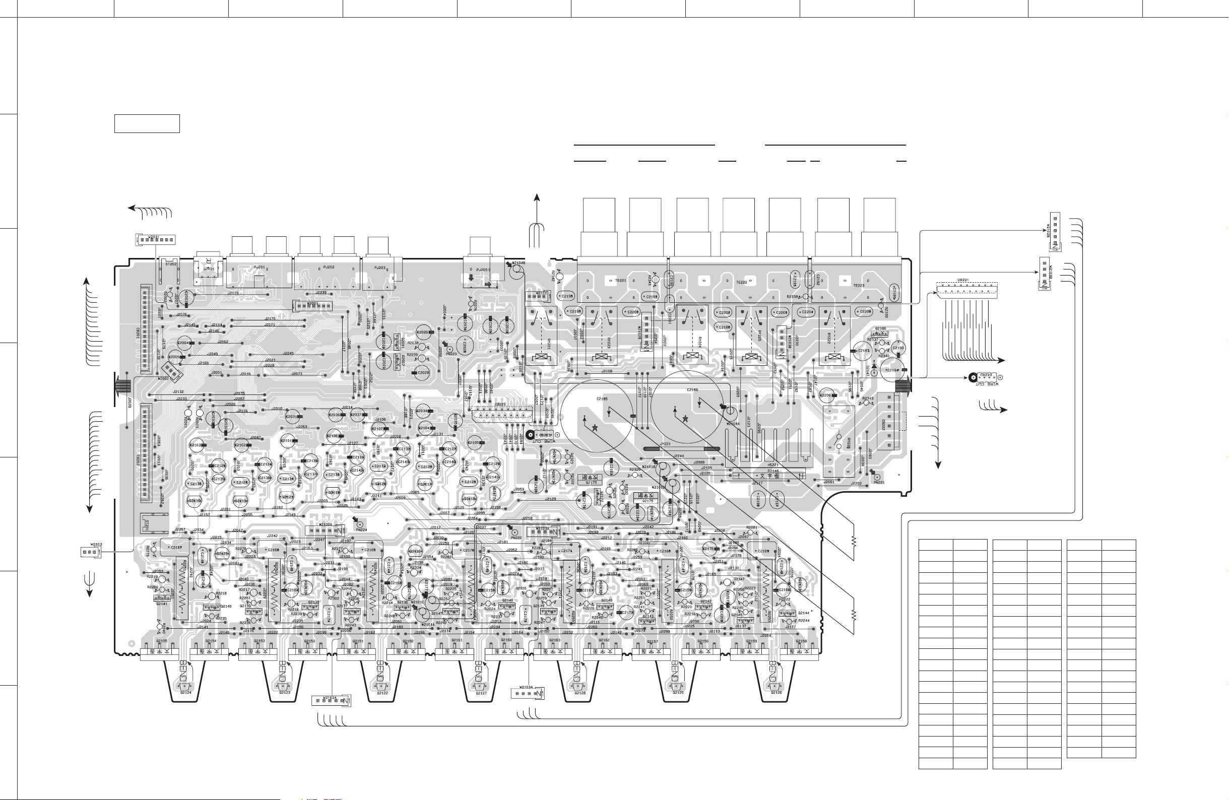
RX-V579/TSR-5790
JIHGFEDCBA
1
Safety measures
• Some internal parts in this product contain high voltages and are dangerous. Be sure to take safety measures during
servicing, such as wearing insulating gloves.
• Note that the capacitors indicated below are dangerous even after the power is turned off because an electric charge
remains and a high voltage continues to exist there. Before starting any repair work, connect a discharging resistor
安全対策
・ この製品の内部には高電圧部分があり危険です。修理の際は、絶縁性の手袋を使用するなどの安全対策を行ってください。
・ 下記のコンデンサには電源を OFF にした後も電荷が残り、高電圧が維持されており危険です。修理作業前に放電用抵抗
(5 k Ω /10 W)を下記の各コンデンサの端子間に接続して放電してください。放電所用時間は各々約 30 秒間です。
MAIN(1)P.C.B. の C2084、C2085
(5 k-ohms/10 W) to the terminals of each capacitor indicated below to discharge electricity. The time required for
discharging is about 30 seconds per each.
MAIN (1)
(Side A)
C2084, C2085 on MAIN (1) P
.C.B.
SPEAKERS
FRONT
2
OPERATION (7)
(CB477)
SUBWOOFER
PRE OUT
1/2
W2104B
HPR
HPE
W2111
HPL
HP_N_DET
+12A
AV1
OPTICAL
(TV)
MAIN (5)
(CB352)
MIC
AUXE
AUXL
AGND
AUXR
-12A
MAIN (3)
(CB272)
3
+3.3DSP
DGND
AV1_D
DGND
AV2_D
DGND
AV3_D
AGND
+12A
AGND
TUL
TUE
TUR
NETR
NETE
NETL
CB201
W2002
AV2
COAXIAL
AV3
COAXIAL
AV4
L/R
W2001
AV5
L/R
AV6
L/R
LR
W2102B
CENTER
SURROUND
LR
+/-+/- +/-+/-+/-
W2103B
SURROUND BACK/
BI-AMP/ZONE B
LR
+/- +/-
PS1_PRT
SPRY_SB
HP_N_DET
HPRY
SPRY_5CH
I_PRT
DGND
AMP_LMT
DC_PRT
AMP_OLV
TRANS_RY
MUTE_SB
VOL_MOSI
VOL_SCK
MUTE_SW
MUTE_5ch
THM2_PRT
DIGITAL
(CB22)
SBR
SBL
SL
SR
C
FL
FL
FR
FR
4
ADR
ADE
ADL
AGND
DAFR
AGND
DAFL
AGND
DASR
DASL
AGND
DASW
DAC
AGND
DASBR
DASBL
-12V
+12V
5
MAIN (2)
(CB252)
CB202
W2102A
CB221
CB223
W2103A
W2104A
RE
BE
CB222
5 k-ohms
-12A
AGND
+12A
10 W
AC_BH
AC_BH
E
E
AC_BL
AC_BL
POWER TRANSFORMER
• Semiconductor Location
Ref no. Location
D2146 G5
D2147 H3
Q2001 D3
Q2002 D4
OPERATION (4)
(CB526)
6
W2101C
BE
RE
W2101A
5 k-ohms
10 W
Q2115 C5
Q2116 B5
Q2117 D5
Q2118 E5
Q2119 C5
Q2120 D5
Q2121 C5
Q2122 D6
Q2123 C6
SL
SR
SBL
C
FL
FL
FR
FR
SBR
Q2124 B6
Q2125 F6
Q2126 G6
Q2127 E6
7
Q2128 F6
Q2129 B5
Q2130 D5
-12A
+40F
+12A
AGND
OPERATION (4)
Ref no. Location
Q2131 C6
Q2132 G6
Q2133 G6
Q2136 D6
Q2137 D6
Q2138 C6
Q2139 C6
Q2140 B6
Q2141 B6
Q2142 G6
Q2143 F6
Q2144 G6
Q2145 G6
Q2146 E6
Q2147 D6
Q2148 F6
Q2149 E6
Q2150 D6
Q2151 D6
Q2152 C6
(CB522)
Ref no. Location
Q2153 C6
Q2154 B6
Q2155 B6
Q2156 G6
Q2157 F6
Q2158 G6
Q2159 G6
Q2160 E6
Q2161 D6
Q2162 F6
Q2163 E6
Q2172 F5
Q2173 E5
Q2174 F5
Q2175 F5
Q2176 F5
Q2177 E5
Q2178 E4
Q2186 H3
98
Page 99
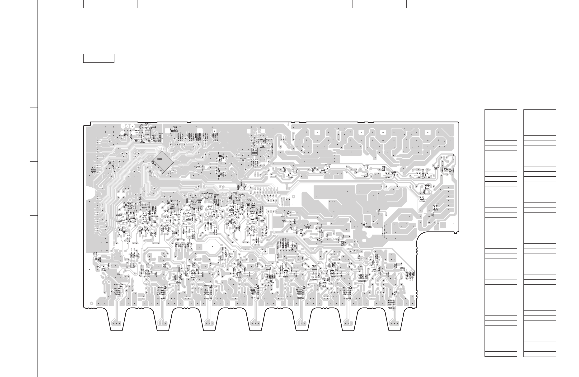
JIHGFEDCBA
1
2
3
4
5
6
7
RX-V579/TSR-5790
MAIN (1)
(Side B)
• Semiconductor Location
Ref no. Location
D2001 D3
D2002 D4
17
IC201
814
61 60
IC203
80
1
41
40
IC202
14
85
D2103 B5
D2104 B5
D2105 D5
D2106 D5
D2107 C6
D2108 C6
D2109 G6
D2110 G6
D2111 H6
20 21
D2112 H6
D2113 E6
D2114 E6
D2115 F6
D2116 F6
D2117 C6
D2118 F6
D2119 G6
D2120 E6
D2121 F6
D2122 D6
D2123 B6
D2124 D5
D2125 C5
D2126 B5
D2127 F5
D2128 G5
D2129 D5
D2130 E5
D2131 F5
D2132 C5
D2133 E5
D2134 F5
D2135 C5
D2136 E5
D2137 F5
D2138 C5
D2139 E5
D2140 E5
D2141 E4
D2142 H4
D2143 F4
D2144 H4
D2145 G4
D2148 G4
D2149 H4
Ref no. Location
D2150 H4
IC201 C3
IC202 E3
IC203 C3
Q2003 C4
Q2004 C4
Q2005 B4
Q2006 D4
Q2007 E4
Q2008 D4
Q2009 D4
Q2010 E3
Q2011 E3
Q2101 C4
Q2102 B4
Q2103 D4
Q2104 E4
Q2105 C4
Q2106 D4
Q2107 C4
Q2108 C5
Q2109 B5
Q2110 D4
Q2111 E5
Q2112 C5
Q2113 D4
Q2114 C5
Q2164 D6
Q2165 C6
Q2166 B5
Q2167 F6
Q2168 G5
Q2169 D6
Q2170 E6
Q2171 F6
Q2179 E4
Q2180 E4
Q2181 H4
Q2182 H4
Q2183 F4
Q2184 F4
Q2185 G4
Q2187 G4
Q2188 G4
Q2189 H4
Q2190 G4
Q2191 H4
99
Page 100
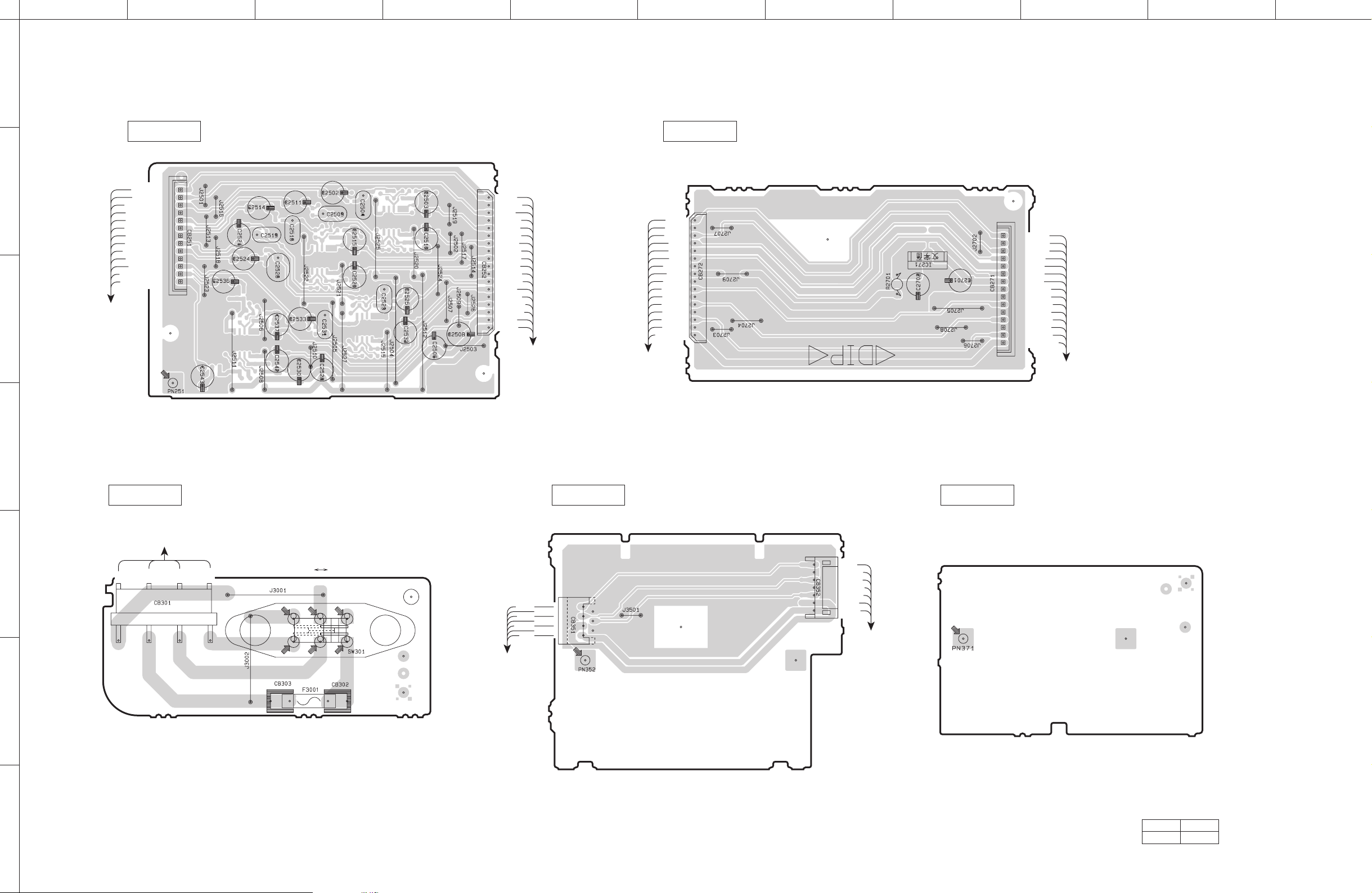
JIHGFEDCBA
RX-V579/TSR-5790
1
MAIN (2)
(CB63)
ADR
ADL
DA-FR
AGND
DA-FL
DA-SR
AGND
DA-SL
DA-SW
AGND
DA-C
DA-SBR
DA-SBL
2
3
DIGITAL
(Side A)
CB251
CB252
ADR
AGND
ADL
AGND
DAFR
AGND
DAFL
AGND
DASR
DASL
AGND
DASW
DAC
AGND
DASBR
DASBL
-12V
+12V
MAIN (1)
(CB202)
+3.3DSP
MAIN (1)
(CB201)
MAIN (3)
NETL
NETE
NETR
TUR
TUE
TUL
AGND
+12V
AGND
AV3_D
DGND
AV2_D
DGND
AV1_D
DGND
CB272
(Side A)
IN COM
OUT
IC271
CB271
NETL
NETE
NETR
TUR
TUE
TUL
+5A
AGND
DGND
AV3_D
DGND
AV2_D
DGND
AV1_D
+3.3DSP
DIGITAL
(CB62)
4
MAIN (4)
R, V, S models
(Side A)
MAIN (5)
(Side A)
MAIN (6)
(Side A)
POWER
TRANSFORMER
5
VI
YE
RE
OR
CB301
VOLTAGE
SELECTOR
110–120V 220–240V
CB303 CB302
+12V
-12V
AUXL
MIC
OPERATION (1)
(CB405)
AGND
AUXR
AUXE
CB351
CB352
MIC
AUXE
AUXL
AGND
AUXR
-12V
+12V
MAIN (1)
(W2001)
6
• Semiconductor Location
7
Ref no. Location
IC271 H3
100
 Loading...