

Page 1
STEREO RECEIVER
RX-485/
RX-485RDS
SERVICE
MANUAL
IMPORTANT NOTICE
This manual has been provided for the useofauthorized YAMAHA Retailers and their selVice personnel.
It
has been assumed that basic selVice procedures inherent to the industry, and more specifically YAMAHA
Products, are already known and understood by the users, and have therefore not been restated.
WARNING:
IMPORTANT:
The data provided
engineering, and selVice depanments
Modifications are, therefore, inevitable and specifications are subject to change without notice or obligation to
retrofit. Should any discrepancy appear
WARNING:
IMPORTANT:
Failure to follow appropriate selVice and safety procedures when selVicing this product
may result in personal injury, destruction
product to perform as specified. For these reasons, we advise all YAMAHA product owners
that any selVice required should be perfonned
appointed selVice representative.
The presentation or saleofthis manual to any individual or firm does not constitute
authorization, cenification or recognition
establish a principle-agent relationship
is
believed tobeaccurate and applicable to the unites) indicated on the cover. The reseach,
Static discharges can destroy expensive components. Discharge any static electricity your
body may have accumulated by grounding yourself
gauge black wires connect
Tum the unit OFF during disassembly and
apply power
of
YAMAHA are continually striving to improve YAMAHA products.
to
exist, please contact the distributor's SelVice Division.
to
this buss).
to
the unit.
of
expensive components, and failureofthe
by
an authorized YAMAHA Retailer or the
of
any applicable technical capabilities, or
of
any form.
to
the ground buss in the unit (heavy
pan
replacement. Recheck all work before you
•
CONTENTS
TO SERVICE PERSONNEL 1
FRONT PANELS 1 2
REAR PANELS 2 3
SPECIFICATIONS 4 5
INTERNAL VIEW 5
DISASSEMBLY PROCEDURES 6
AMP ADJUSTMENTS 6
TEST MODE 7
TUNER ADJUSTMENTS 8
RX-485 BLOCK DIAGRAM 12 13
RX-485RDS BLOCK DIAGRAM 14 15
11
RX-485
RX-485RDS
RX·485 DISPLAY DATA
RX·485RDS DISPLAY DATA
FRONT END PACK
TEST POINT WAVEFORMS
PRINTED CIRCUIT BOARD
SCHEMATIC DIAGRAM
PARTS LIST
REMOTE CONTROL TRANSMITTER
~-COM
~-COM
DATA
2.95K-223
DATA
YAMAHA
YAMAHA
P.O.Box1,Hamamatsu,Japan
IQl
®
PrintedinJapan
16-17
18-19
20
21
22
23
24-33
34-39
40-48
49
CORPORATION
'94.4
Page 2
RX-485/RX-485RDS
•
TO
SERVICE
1.
Critical Components Information.
Components having special characteristics
mustbereplaced with parts having specifications equal
those originally installed.
2.
Leakage Current Measurement (For 120V Models Only).
When service
that
all
from supply circuits.
• Meter impedance should
by
0.15J.lF.
• Leakage current must not exceed 0.5mA.
Be
sure to test for leakage with theACpluginboth
•
polarities.
has
exposed conductive surfaces are properly insulated
PERSONNEL
are
marked
been completed. itisimperativetoverify
be
equivalent to 1500
ohm
and
shunted
AC
to
WALL
OUTLET
@]~
EQUIPMENT TESTER
UNDER
TEST EQUIVALENT
I~~
INSULATING
TABLE
LEAKAGE
OR
I
WARNING: CHEMICAL CONTENT NOTICEI
The solder usedinthe production of this product contains LEAD.Inaddition, other electrical/electronic and/or
plastic (where applicable) components may also contain traces of chemicals found by the California Health and
Welfare Agency (and possibly other entities)
DO
NOT PLACE SOLDER, ELECTRICAL/ELECTRONIC
ANY REASON WHAT SO EVER!
Avoid prolonged, unprotected contact between solder and your skin! When soldering, do not inhale solder fumes or
expose eyes to solder/flux vapor!
If you come in contact with solder or components located inside the enclosure of this product, wash your hands
before handling food.
to
cause cancer and/or birth defects or other reproductive harm.
OR
PLASTIC COMPONENTSINYOUR MOUTH FOR
•
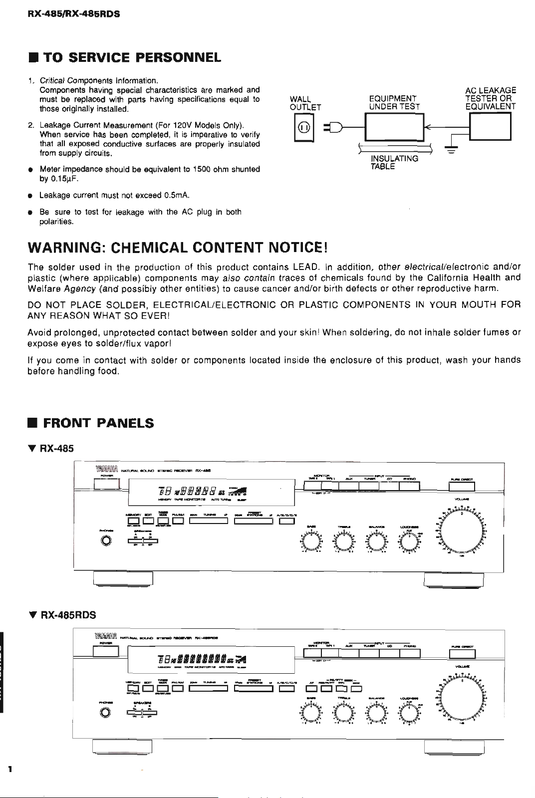
FRONT
~
RX·485
~
RX·485RDS
PANELS
nl
l
o
r
nl
I
o
i 8
.83
I
78
•••••'•••
83
S
BEl.:
;;';l1lI
.:;;4!
"""""""
.......
I I 1 I
--~--
,
AUK
~
I I I 1
CD
I
"""""""
....
I I I I
--~--
'WI'
AUK
~
CD
I I I I
I
• 0 • • 0 • • 0 • • I
. .
,
. . .
0
- • •
0'
-.
C'
• +~• • •
~
........a
....-
V
o
r
-:-
0
a •
··
. .
,.
I
0
I
1
I
I
l
Page 3
~
RX-485/RX-485RDS
'OiCiIo 0
--_
.....
~
~_c::
,;;.::
0000
DODD
000
aOD
ODD
"='
......
Do
1IlIl1I'M
\
o
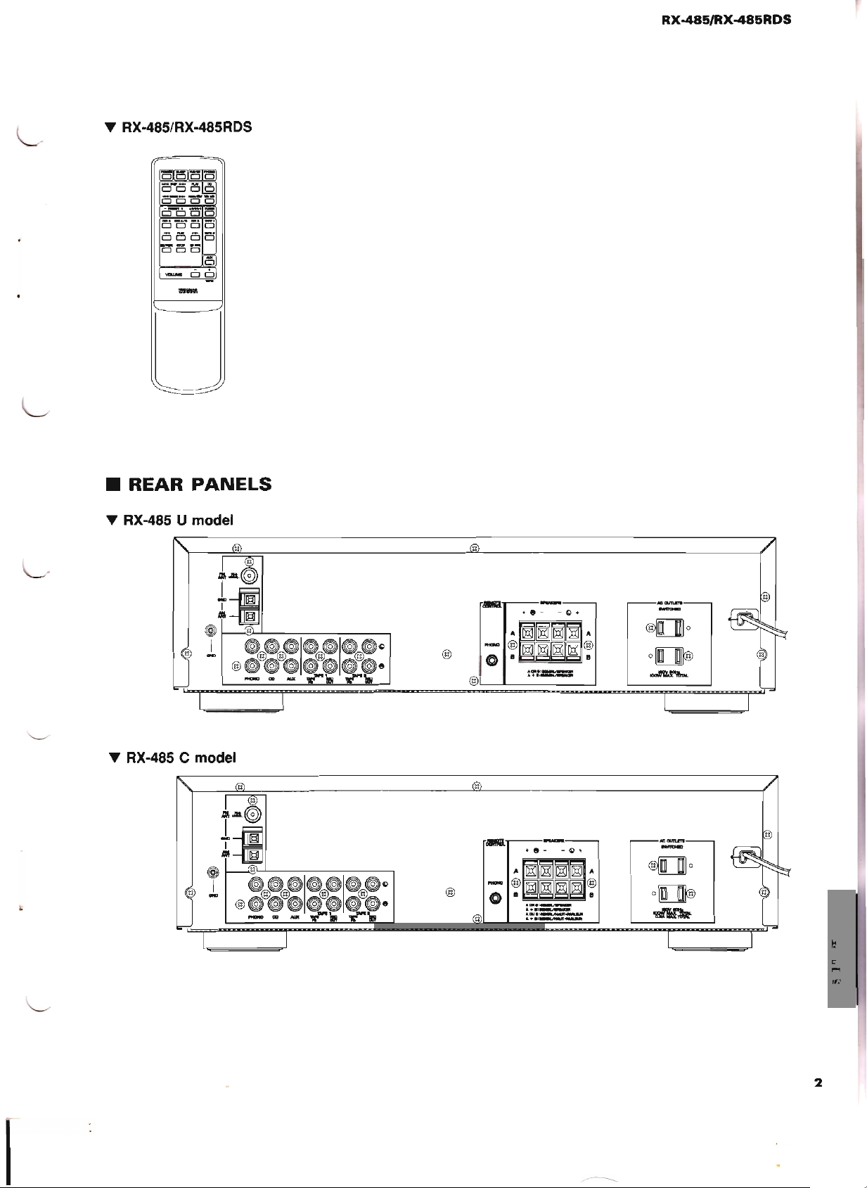
RX-485/RX-485RDS
==-
Ci
Ci
0
~
•
REAR
~
RX-485 U model
~ RX-485 C model
PANELS
""
+8-
-Q+
@
........
-
r
2
Page 4
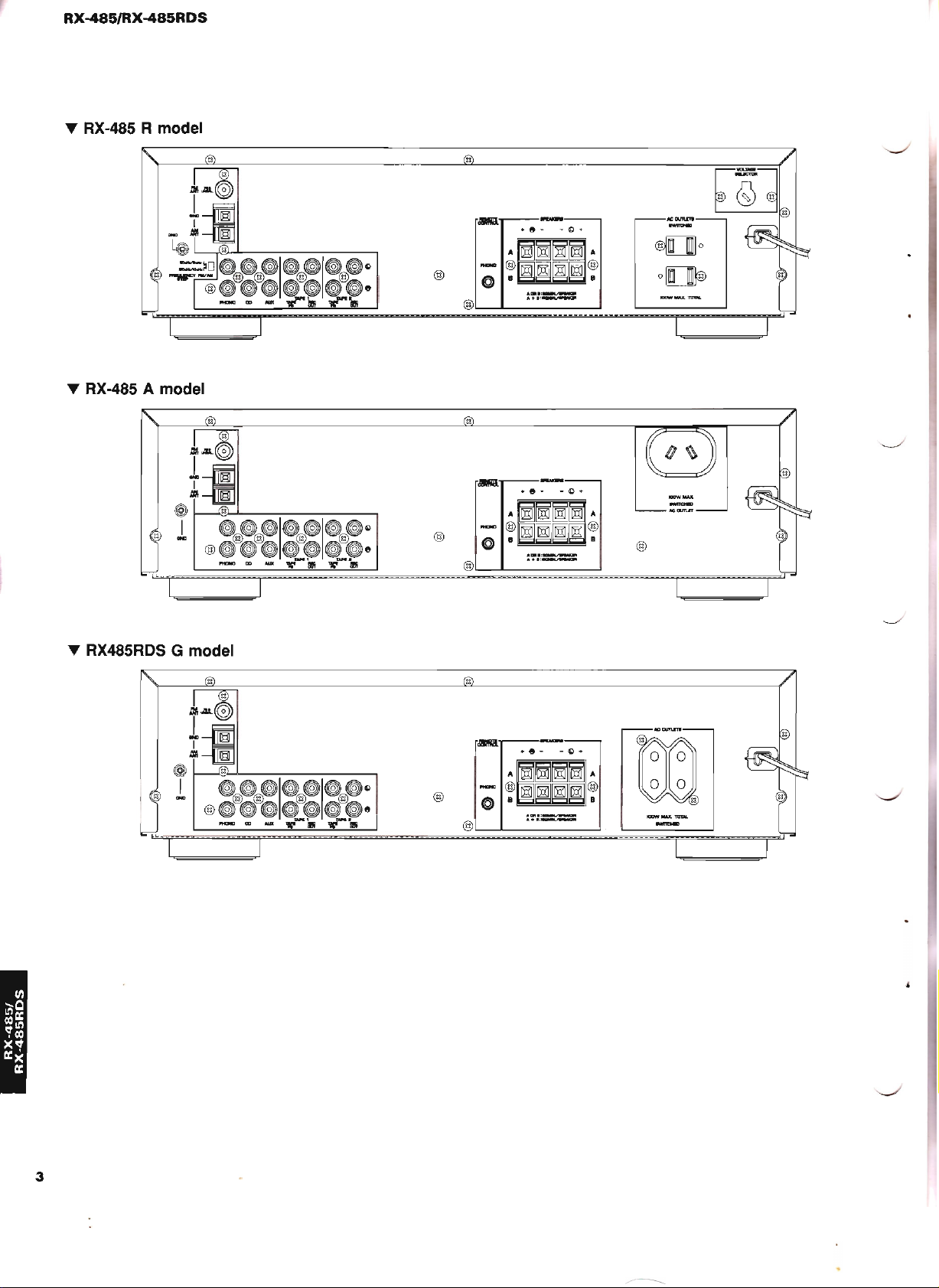
RX-485/RX-485RDS
'Y
RX-485 R model
'Y
RX-485 A model
+8-
-G+
A
~
@
-@
0
@
~
~
~
8
Ami.:.....,.....
A+.:
...........
~ ~
~ ~
A
@
cU°
o~
'Y
RX485RDS G model
3
Page 5
•
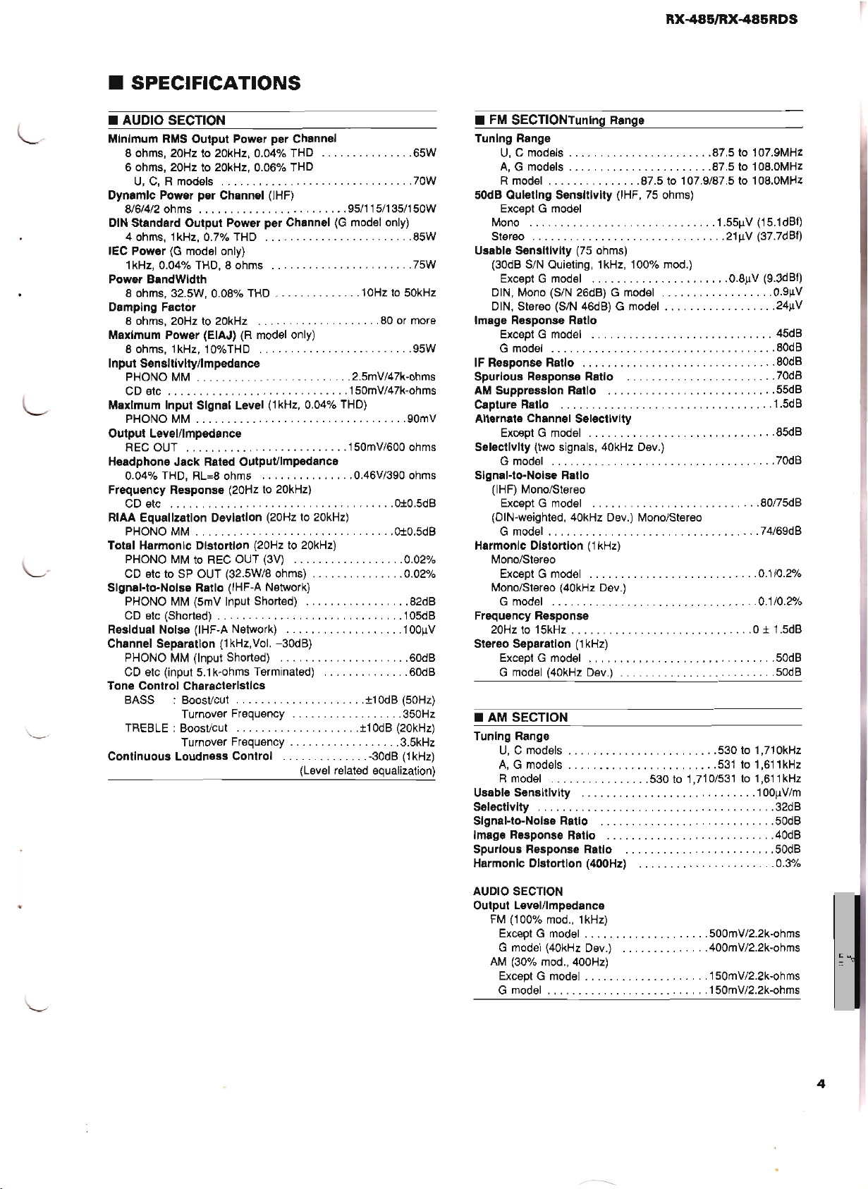
SPECIFICATIONS
•
AUDIO
Minimum
8 ohms, 20Hz to 20kHz, 0.04%
6 ohms, 20Hz
Dynamic
8/6/4/2 ohms 95/115/1351150W
DIN Standard
4 ohms, 1kHz, 0.7%
IEC Power
1kHz, 0.04% THO, 8 ohms 75W
Power BandWidth
8 ohms, 32.5W, 0.08%
Damping Factor
8 ohms, 20Hz
Maximum Power (EIAJ)
8 ohms, 1kHz, 10%THO 95W
Input
PHONO
CO
Maximum
PHONO
Output
REC OUT 150mV/600 ohms
Headphone
0.04% THO, RL=8 ohms 0.46V/390 ohms
Frequency Response (20Hz
CO
RIAA Equalization Deviation (20Hz
PHONO
Total Harmonic
PHONO
CD etc to SP OUT (32.5W/8 ohms) 0.02%
Signal-to-Noise Ratio (IHF-A Network)
PHONO
CD etc (Shorted) 105dB
Residual Noise (IHF-A Network)
Channel Separation
PHONO
CD
Tone
BASS : Boost/cut ±10dB (50Hz)
TREBLE : Boost/cut
Continuous
SECTION
RMS
Output
Power per Channel
THO
to
U,C,R models 70W
Power per Channel (IHF)
(G
Sensitivity/Impedance
MM
etc 150mV/47k-ohms
Input
MM
Level/Impedance
etc 0±0.5dB
MM
MMtoREC
MM
MM
etc (input
Control
20kHz, 0.06%
Output
Power per Channel(Gmodel only)
THO
model only)
THO
to
20kHz
(R
Signal Level(1kHz, 0.04%
Jack
Rated Output/Impedance
Distortion
OUT (3V) 0.02%
(5mV Input Shorted) 82dB
(1
kHz,Vol. -30dB)
(Input Shorted) 60dB
5.1
k-ohms Terminated) 60dB
Characteristics
Turnover Frequency 350Hz
Turnover Frequency 3.5kHz
Loudness
Control
THO
model only)
to
20kHz)
to
20kHz)
(20Hzto20kHz)
(Level related equalization)
1
OHzto50kHz
80
2.5mV/47k-ohms
THO)
±1
OdB
-30dB(1kHz)
65W
85W
or more
90mV
0±0.5dB
100IlV
(20kHz)
RX-485/RX-485RDS
•
FM
SECTIONTunlng
Tuning Range
U,
C models 87.5to107.9MHz
A,
G models 87.5to108.0MHz
R model 87.5
SOdB
Quieting
Except G model
Mono
Stereo
Usable Sensitivity (75 ohms)
(30dB
Except G model 0.8IlV (9.3dBf)
DIN,
OIN,
Image Response Ratio
ExceptG
G model 80dB
IF Response Ratio 80dB
Spurious
AM Suppression Ratio 55dB
Capture Ratio 1
Alternate Channel Selectivity
Except G model 85dB
Selectivity (two signals, 40kHz Dev.)
G model 70dB
Signal-to-Noise Ratio
(IHF) Mono/Stereo
ExceptG
(DIN-weighted, 40kHz
G model 74/69dB
Harmonic Distortion
Mono/Stereo
Except G model 0.1/0.2%
Mono/Stereo (40kHz Dev.)
G model 0.1/0.2%
Frequency Response
20Hz
Stereo Separation
Except G model 50dB
G model (40kHz Dev.) 50dB
AM
SECTION
•
Tuning Range
U,
A,
R model 530 to 1,710/531to1,611
Usable Sensitivity 100IlV/m
Selectivity 32dB
Signal-to-Noise Ratio 50dB
Image Response Ratio 40dB
Spurious Response Ratio 50dB
Harmonic Distortion (400Hz) 0.3%
Sensitivity
SIN
Quieting, 1kHz, 100% mod.)
Mono (S/N 26dB) G model 0.9IlV
Stereo (S/N 46dB) G model
mod~
Response Ratio
mod~
to
15kHz 0 ± 1.5dB
C models 530to1,710kHz
G models
(1
(1
kHz)
kHz)
Range
(IHF,75ohms)
Oev.)
Mono/Stereo
to
107.9/87.5to108.0MHz
1.551lV(15.1
211lV
(37.7dBf)
80/75dB
531to1,611
dBf)
241lV
45dB
70dB
.5dB
kHz
kHz
AUDIO SECTION
Output Level/Impedance
FM
(100% mod., 1kHz)
Except G model 500mV/2.2k-ohms
G model (40kHz
AM
(30% mod., 400Hz)
Except G model 150mV/2.2k-ohms
G model 150mV/2.2k-ohms
Oev.)
400mV/2.2k-ohms
4
Page 6
RX-486/RX-485RDS
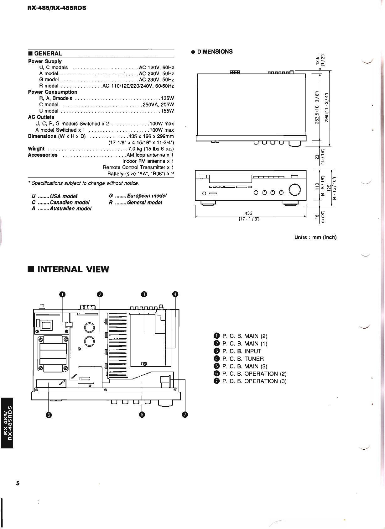
• GENERAL
Power
Supply
U,
C models
A model :
G model
R model
Power
Consumption
R,A,Bmodels 135W
C model 250VA, 205W
U model 155W
AC Outlets
U,C,R,
A model Switched x 1 100W max
Dimensions (W x H x
Weight 7.0
Accessories
..
Specifications subjecttochange without notice.
U USA
C Canadian
A
G models Switched x 2 100W max
D)
.........•.............
model
Australian
model
model
AC110/120/220/240V, 60/50Hz
(17-1/8" x 4-15/16" x 11-3/4")
Remote Control Transmitter x 1
Battery (size "AA", "R06") x 2
G European
R •....... General
AC
120V, 60Hz
AC
240V, 50Hz
AC
230V, 50Hz
.435 x 126 x 299mm
kg
(151bs 6 oz.)
AM
loop antenna x 1
FM
Indoor
antenna x 1
model
model
• DIMENSIONS
coCo
...........
!:!!
•
INTERNAL
VIEW
o
•
•
o
•
•
•
P.C.B.
P.C.B.
P.C.B.
P.C.B.
P.C.B.
P.C.B.
P.C.B.
MAIN
(2)
MAIN
(1)
INPUT
TUNER
MAIN
(3)
OPERATION
OPERATION
(2)
(3)
Units:
mm (Inch)
5
Page 7
•
DISASSEMBLY
(Remove parts in the order as numbered.)
1.
RemovalofTop Cover
Remove 4 screws
2.
RemovalofFront Panel
a.
Remove 5 knobs.
b. Remove 6 screws
Top Cover
(Q))
(Q))
PROCEDURES
and 3 screws
in Fig.
1.
:,,----
-:=-~
-----.-
=-~~~
>~
(CV)
in Fig.
CV
-~
?i
-------~Q)
RX-486/RX-485RDS
3.
RemovalofRear
1.
Remove 15 screws
* The
P.
C. B. MAIN, INPUT, &
removed
in
Panel
(®)
this state.
in
Fig.
2.
TUNER
can be
Fig. 2
Fig. 1
•
AMP
ADJUSTMENTS
• ConfirmationofInling current.
After Power is turned on.
Confirm that the voltages across R137 (L ch), R138
(R ch) are between 0.1-3mV.
If they exceeds
and R132
0.1-3mV.
0.1mV- 3mV
R137,
3.1
mV, open (cut off)
(R
ch), and reconfirm voltage is between
(DC)
R131
138
R132
R131
____
Cut
(L ch)
• Checking and Parts ReplacementofP.C.B. MAIN
a.
Disconnect the power cord from the AC outlet.
b. Remove 3 screws fixing the Speaker terminal and Heat Sink.
c.
Remove 4 screws fixing the Main Unit.
d. Detach 1 connector terminal (CB104)
e.
Place the Main Unit on its side as showninFig.
f.
Operating checks can be taken by shorting between follow-
in
Fig.
ing test points
A.
in
Fig.
A.
B.
(1)
:
,
••••••
FRONT
p.e.B. MAIN
Fig. A
(1)
Short Point
TP101
TP1
03
TP105
~
TP102
~
TP104
~
TP106
Fig. B
6
Page 8
RX-485/RX-485RDS
•
TEST
MODE
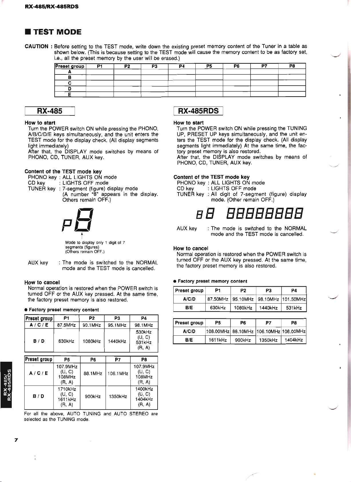
CAUTION:
Before setting to the TEST mode, write down the existing preset memory content of the Tunerina table
shown below. (Thisisbecause settingtothe TEST mode will cause the memory content tobeas factory set,
all
i.e.,
the preset memorybythe user willbeerased.)
Preset group
A
B
C
0
E
P1
P2
RX-485
Howtostart
Turn the POWER switchONwhile pressing the PHONO,
AlBICIDIE keys simultaneously, and the unit enters the
TEST mode for the display check. (All display segments
light immediately)
by
After that, the DISPLAY mode switches
PHONO, CD, TUNER, AUX
Contentofthe
PHONO key : ALL LIGHTS
CD
key : LIGHTS OFF mode
TUNER key : 7-segment (figure) display mode
TEST
mode
(A
number "8" appearsinthe display.
Others remain OFF.)
key.
key
ON
mode
means of
P3
P4 P5
P6
P7
P8
I RX-485RDS I
Howtostart
Turn
the
UP,
ters
segments light immediately) At the same time, the factory preset memory
After that, the DISPLAY mode switches by means of
PHONO,
Content
PHONO
CD
TUNER
POWER switch
PRESETUPkeys simultaneously, and the unit enthe
TEST mode for the display check. (All display
CD,
TUNER, AUX
of
the TEST mode key
key
key
: ALL LIGHTS
: LIGHTS OFF mode
key
: All digit of 7-segment (figure) display
mode. (Other remain OFF.)
ON
while pressing the TUNING
is
also restored.
key.
ON
mode
as
B
P~l
Modetodisplay only 1 digit of 7
segments (figures)
(Others remain OFF.)
AUX key
to
How
Normal operation
turned OFF or the AUX key pressed. At the same time,
the factory preset memory
• Factory preset memory content
Preset
group
A/C/E
BID
Preset
group
A/C/E
BID
For all the above, AUTO TUNING and AUTO STEREO are
selected as the TUNING mode.
: The modeisswitchedtothe NORMAL
mode and the TEST mode
cancel
is
P1
87.5MHz
630kHz
P5
107.9MHz
(U, C)
108MHz
A)
(R,
1710kHz
(U,
C)
1611
kHz
A)
(R,
'
t
is
cancelled.
restored when the POWER switch
is
also restored.
P2
90.1MHz 95.1MHz
1080kHz 1440kHz
P6
88.1MHz 106.1MHz
900kHz 1350kHz
P3 P4
98.1MHz
530kHz
(U,
531kHz
(R,
P7
P8
107.9MHz
(U,
108MHz
(R,
1400kHz
(U,
1404kHz
(R,A)
C)
A)
C)
A)
C)
BB
AUX
key
to
How
Normal operation
turned OFF or the AUX key pressed. At the same time,
the factory preset memory
• Factory preset memory content
is
Preset group
AlC/D
B/E
Preset group
AlC/D
B/E
: The modeisswitched to the NORMAL
cancel
87.50MHz
108.00MHz
BBBBBBBB
and
mode
is
P1
630kHz
P5
1611kHz
the TEST modeiscancelled.
restored when the POWER switch
is
also restored.
P2
95.10MHz
1080kHz 1440kHz 531kHz
P6
88.10MHz 106.10MHz
900kHz 1350kHz 1404kHz
P3
98.10MHz
P7 P8
is
P4
101.50MHz
108.00MHz
7
Page 9
•
TUNER
RX-486/RX-485RDS
ADJUSTMENTS
• Measuring Instruments
FM
signal generator
Stereo signal generator (SSG)
AM
signal generator (AM
Distortion meter (DIST.
AC voltmeter (ACVM)
DC
voltmeter (DCVM)
Oscilloscope
Low
pass filter (YLF-15, fc:15kHz)
Oscillator
(FM
M)
SG)
SG)
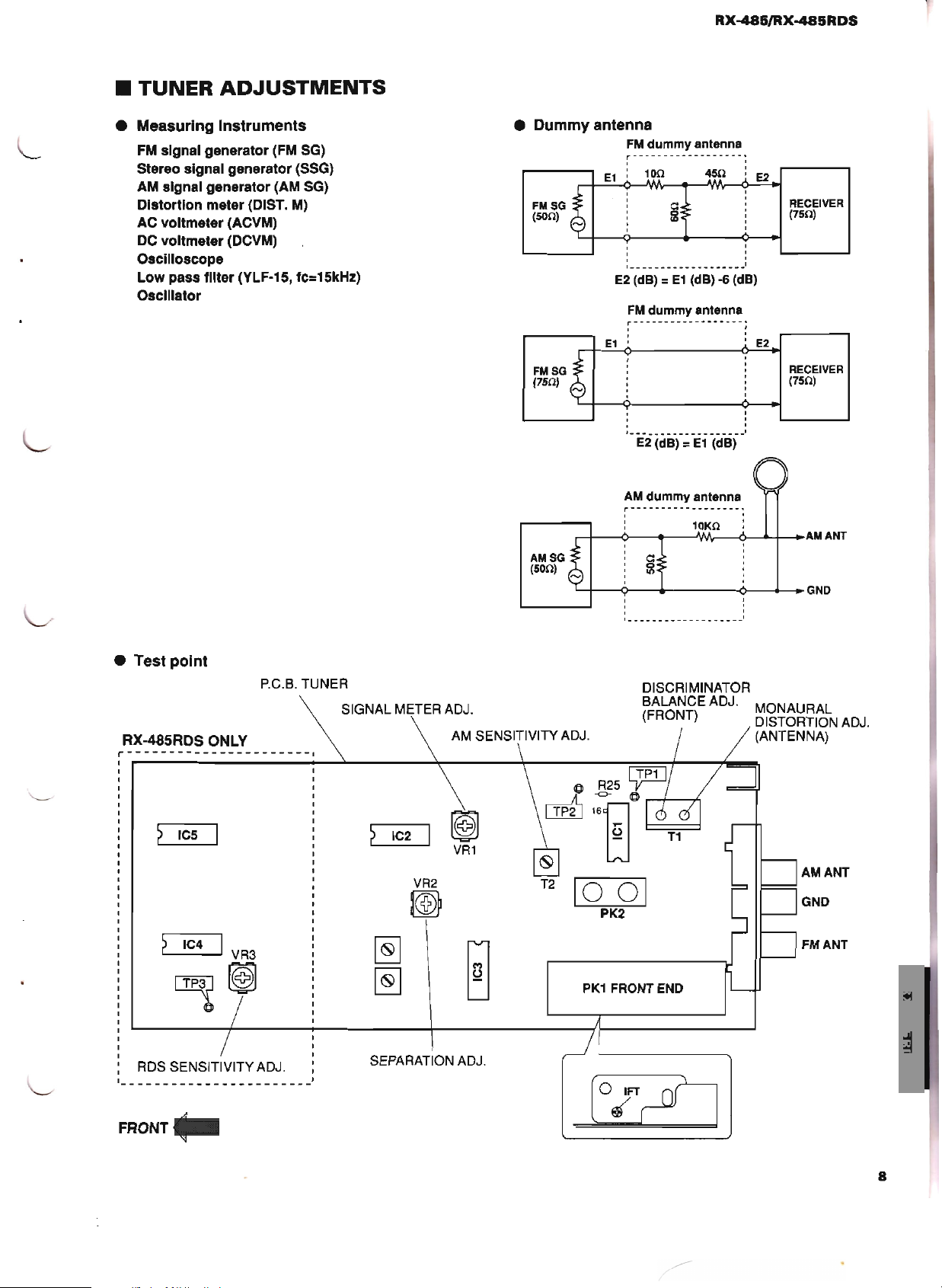
• Dummy antenna
FM
r------------------·
I I
:
FM
SG
(SOO)
I I
I I
I I
I
E2
(dB) =E1(dB) -6 (dB)
FM
r------------------·
I I
I I
E1
I I
FMSG
(7S0)
I I
I I
I I
I.
E2 (dB) =E1(dB)
AM
r------------------·
I I
~-__O_--+--.JW\r____o_-+_
AMSG
(SOO)
L......+---O--
:
I I
I I
I I
I
dummy
100
dummy
dummy
antenna
4S0:
------------~
antenna
antenna
10KO:
.........
-----O--~
------------~
.1
E2
E2
o
RECEIVER
(7S0)
RECEIVER
(7S0)
....
AM
ANT
....
GND
• Test point
P.C.B. TUNER
RX-485RDS ONLY
r----------------------
> IC5 I
> IC4 I
ITP~
RDS SENSITIVITYADJ.
VR3
~
SIGNAL METER ADJ.
>
VR2
~
~
~
SEPARATION ADJ.
~
T2
10
PK1
DISCRIMINATOR
BALANCE ADJ. MONAURAL
(FRONT) DISTORTION ADJ.
(ANTENNA)
T1
01
PK2
FRONT END
AMANT
GND
FMANT
FRONT
~::(///I
8
I
Page 10
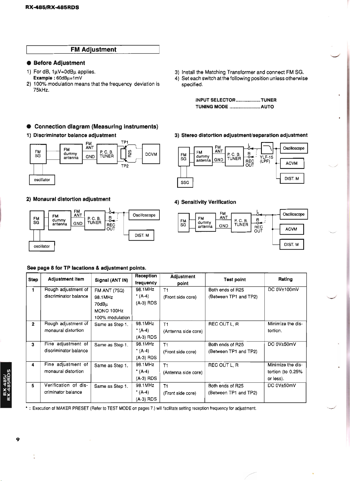
RX-486/RX-486RDS
FM
Adjustment
• Before Adjustment
1)
For
dB,1Jl
Example:
2)
100%
V=OdBJl
60dBJl=1 mV
modulation
applies.
means
that
the
frequency
deviation
75kHz.
• Connection diagram (Measuring Instruments)
1)
Discriminator balance adjustment
TP1
DCVM
TP2
FM
SG
FM
dummy
antenna
FM
ANT
GND
P.C.B.
TUNER
3) Install
4)
is
the
Set
each
specified.
Matching
switchatthe
Transformer
following
and
position
connect
unless
FM
SG.
otherwise
INPUT SELECTOR TUNER
TUNING MODE AUTO
3)
Stereo distortion adjustment/separation adjustment
...----
~~mmy
antenna
FM
ANTP.C.
GND
TUNER
L.-_......l
L
B.
R
REC
OUT
2)
Monaural distortion adjustment
...---
FM
dummy
antenna
...
FM
ANT
P.C.
TUNER
GND
L
I
I
R
B.
REC
OUT
see page 8 forTPlacations & adjustment points.
Step
5
* :
Adjustment Item
Rough adjustment of
1
discriminator balance
Rough adjustment of
2
monaural distortion
Fine
3
discriminator balance
Fine
4
monaural distortion
Verificationofdiscriminator balance
ExecutionofMAKER
adjustment
adjustment
PRESET
Signal (ANT IN)
FM
ANT (750)
98.1MHz
70dBJl
MONO 100Hz
100% modulation
Same as Step 1.
of
Same as Step 1.
of
SameasStep 1.
Same as Step 1.
(RefertoTEST
Reception
frequency
98.1MHz
* (A-4)
(A-3) RDS
98.1MHz
* (A-4)
(A-3) RDS
98.1MHz
* (A-4)
(A-3) RDS
98.1MHz
* (A-4)
(A-3) RDS
98.1MHz
* (A-4)
(A-3) RDS
MODEonpages
Adjustment
T1
(Front side core)
T1
(Antenna side core)
T1
(Front side core)
T1
(Antenna side core)
T1
(Front side core)
7.)
will
facilitate
4)
Sensitivity Verification
FM
dummy
antenna
point
Both ends of R25
(Between
REC OUTL,R
Both ends of R25
(Between
REC OUTL,R
Both ends of R25
(Between
setting
reception
frequency
FM
ANT
GND
Test point
TP1
TP1
TP1
for
P.C.B.
TUNER
L...-_---J
and TP2)
and TP2)
and TP2)
adjustment.
L
R I
REC
OUT
DC OV±100mV
Minimize the distortion.
DC
Minimize the dis-
tortion (to 0.25%
or less).
DC
Rating
OV±50mV
OV±50mV
9
Page 11
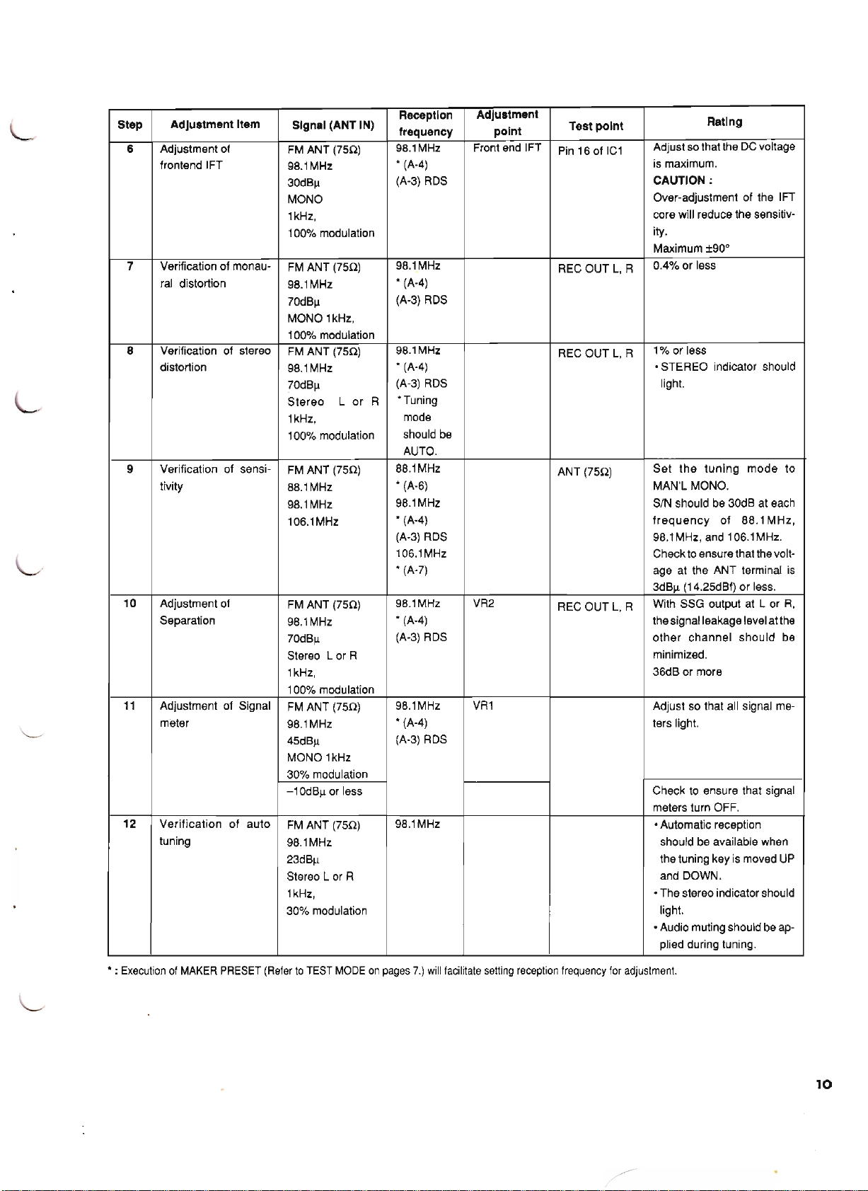
Step
Adjustment
Item
6 Adjustment of
frontend
1FT
7 Verification of monau-
ral distortion
Verification of stereo
8
distortion
Verification of sensi-
9
tivity
10 Adjustment of
Separation
11
Adjustment of Signal
meter
12
Verification
tuning
of auto
Signal (ANT IN)
FM
ANT (750)
98.1MHz
30dBJl
MONO
1kHz,
100% modulation
FM
ANT (750)
98.1MHz
70dBJl
MONO 1kHz,
100% modulation
FM
ANT (750)
98.1MHz
70dBJl
Stereo
or
L
1kHz,
100% modulation
FM
ANT (750)
88.1MHz
98.1MHz
106.1MHz
FM
ANT (750)
98.1MHz
70dBJl
Lor
Stereo
R
1kHz,
100% modulation
FM
ANT (750)
98.1MHz
45dBJl
MONO 1kHz
30% modulation
-1
OdBJl
or less
FM
ANT (750)
98.1MHz
23dBJl
Stereo
Lor
R
1kHz,
30% modulation
R
Reception
frequency
98.1MHz
* (A-4)
(A-3) RDS
98.1MHz
* (A-4)
(A-3) RDS
98.1MHz
* (A-4)
(A-3) RDS
o Tuning
mode
should be
AUTO.
88.1MHz
o (A-6)
98.1MHz
* (A-4)
(A-3) RDS
106.1MHz
o (A-7)
98.1MHz
* (A-4)
(A-3) RDS
98.1MHz
* (A-4)
(A-3) RDS
98.1MHz
Adjustment
point
Front end
VR2
VR1
1FT
Test
point
Pin 16 of
REC OUT
REC OUT
ANT (750)
REC OUT
IC1
Adjust so thattheDCvoltage
is maximum.
CAUTION:
Over-adjustment of the
core will reduce the sensitivity.
Maximum ±90°
0.4% or less
L,
R
1% or less
L,
R
o STEREO indicator should
light.
Set
the
MAN'L MONO.
SIN
should be 30dB at each
frequency
98.1
MHz, and 106.1 MHz.
to
Check
ensurethatthe voltage at the ANT terminal
3dBJl (14.25dBf) or less.
With SSG output at L or
L,
R
thesignalleakagelevelatthe
other
channel
minimized.
36dB or more
Adjust so that all signal meters light.
Check to ensure that signal
meters turn OFF.
o Automatic reception
should be available when
the tuning key is moved
and DOWN.
o The stereo indicator should
light.
o Audio muting should be ap-
plied during tuning.
Rating
tuning
of
1FT
mode
88.1 MHz,
should
to
is
R,
be
UP
* :
ExecutionofMAKER
PRESET
(RefertoTEST
MODEonpages
7.)
will
facilitate
setting
reception
frequency
for
adjustment.
~
/
10
Page 12
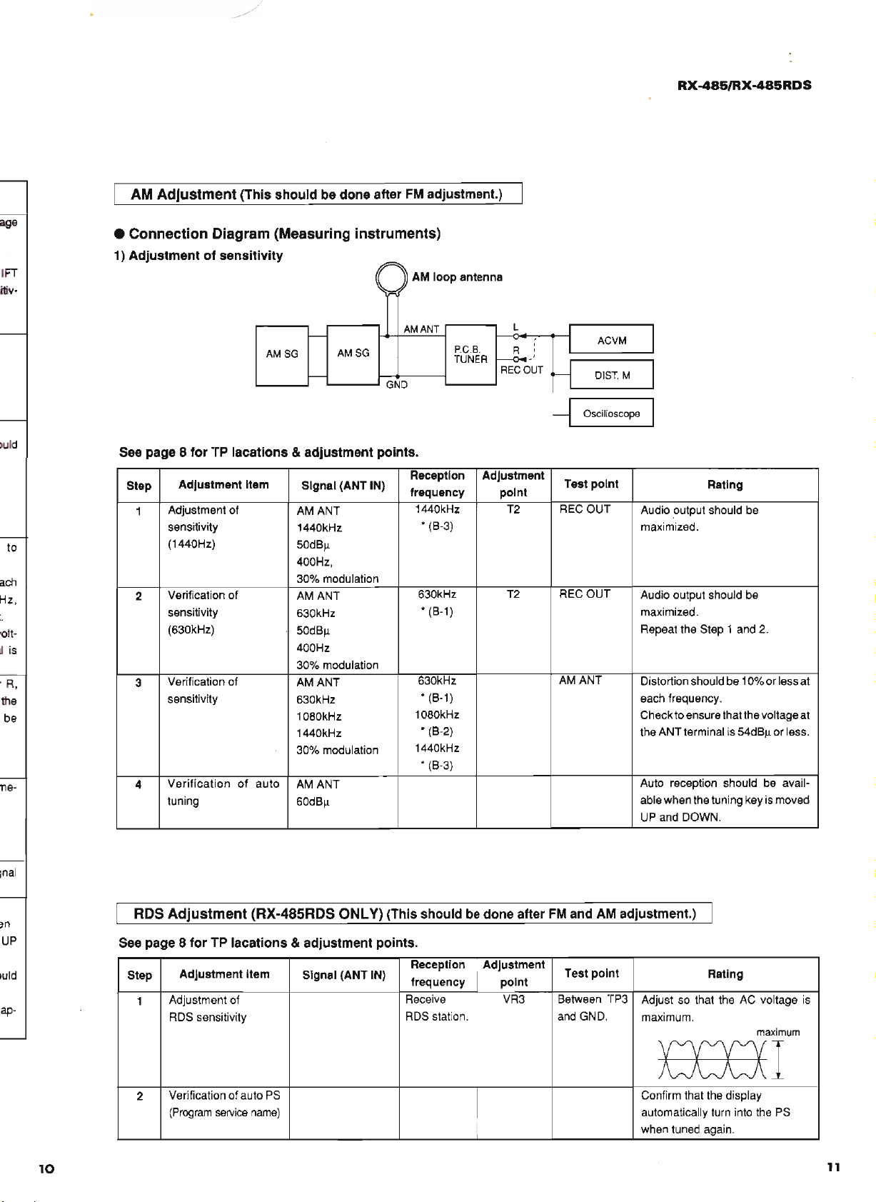
AM
Adjustment (This should be done after
FM
adjustment.)
RX-485/RX-485RDS
age
1FT
ach
z,
o -
~
.
R,
be
e-
• Connection Diagram (Measuring instruments)
1)
Adjustmentofsensitivity
oAM
,.."
f---
AMSG
d
o
is
e
See page 8
Step
Adjustment of
1
sensitivity
(1440Hz)
Verification of
2
sensitivity
(630kHz)
Verification of
3
sensitivity
Verificationofauto
4
tuning
forTPlacations &adjustment points.
Adjustment
Item
AMSG
r--
Signal
(ANT
AMANT
1440kHz
50dBJl
400Hz,
30% modulation
AMANT
630kHz
50dBJl
400Hz
30% modulation
AMANT
630kHz
1080kHz
1440kHz
30% modulation
AMANT
60dBJl
GNO
IN)
loop
antenna
AMANT
P.C.B.
TUNER
Reception
frequency
1440kHz
* (B-3)
630kHz T2
* (B-1)
630kHz
* (B-1)
1080kHz
* (B-2)
1440kHz
* (B-3)
Adjustment
L
-
R
~_'
RECOUT
point
T2
I
I
I
I
~
Oscilloscope
Li
Test
REC OUT
REC OUT
AMANT
ACVM
OIS1.
point
I
M
I
I
Rating
Audio output should be
maximized.
Audio output should be
maximized.
Repeat the Step 1 and
Distortion should be 10% or less at
each frequency.
Check to ensurethatthevoltageat
the ANT terminal is 54dBJl or less.
Auto reception should be availablewhen the tuning key is moved
UP and DOWN.
2.
m
UP
ap-
al
RDS
Adjustment (RX-485RDS ONL
See page 8
Id
Step
1
forTPlacations & adjustment points.
Adjustment
Adjustment of
RDS sensitivity
Item
Signal
V)
(ANT IN)
(This shouldbedone afterFMand
Reception
frequency
Receive
RDS station. and GND.
Adjustment
point
VR3
Test
Between TP3
AM
adjustment.)
point
Rating
Adjust so that the AC voltage is
maximum.
maximum
Y2fJ2AI
Verification of auto PS Confirm that the display
2
(Program
10
service
name)
automatically turn into the PS
when tuned again.
11
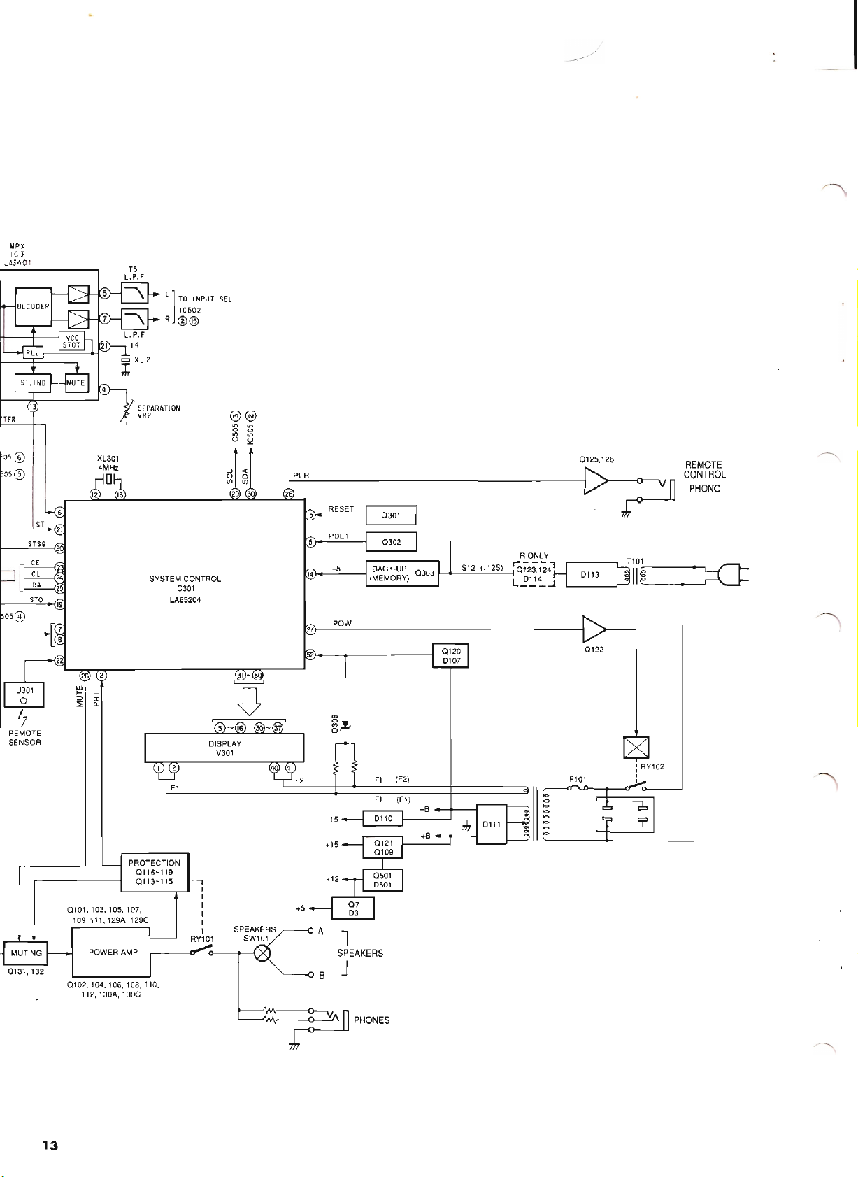
Page 13
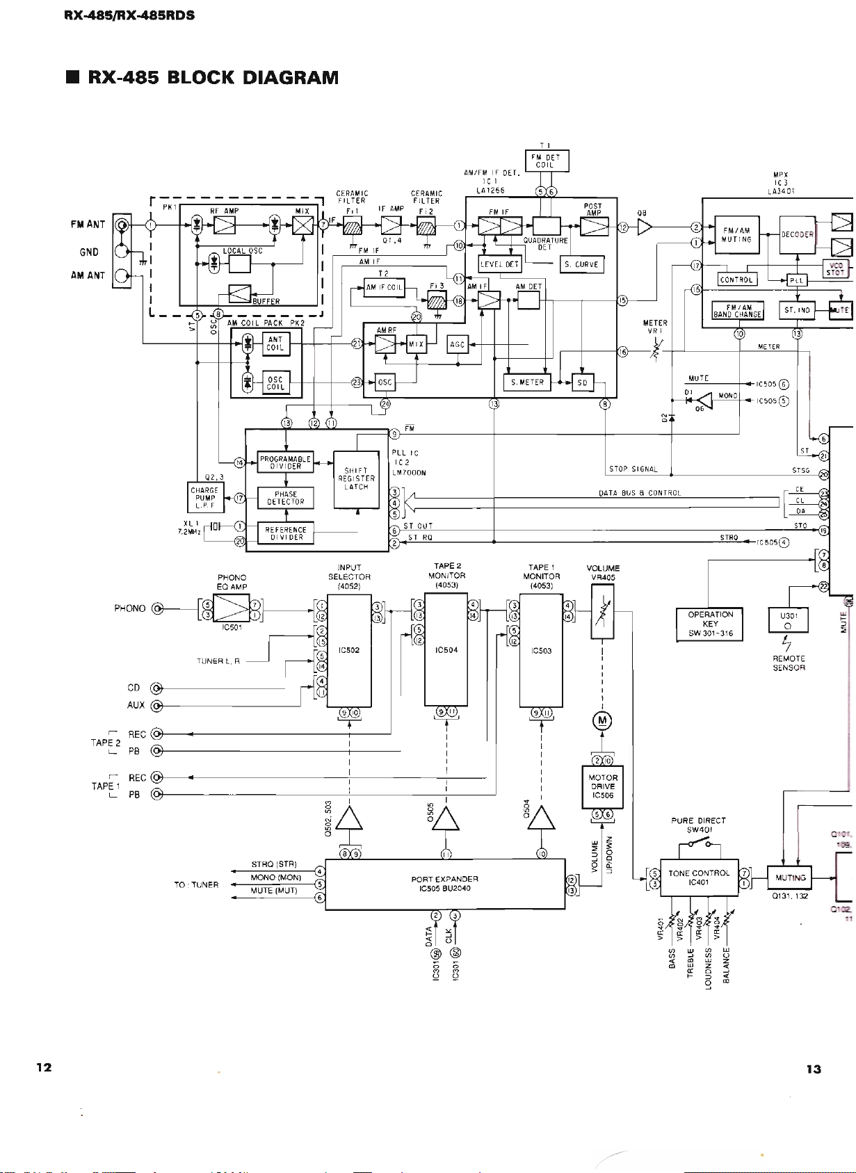
RX-485/RX-485RDS
•
RX-485
BLOCK
DIAGRAM
FMANT
GND
AM
ANT
PHONO
CERAMIC
FILTER
Fi 1
INPUT
SELECTOR
(4052)
TAPE 2
MONITOR
(4053)
AM/FMIFDET.
I C 1
LA1266
TAPE
MONITOR
(4053)
MPX
IC3
LA340
LM.:.:..U=--T...::EO---_-+IC
oI
MONO
t----'-c.=.:..:..:+-o
06
o
'"
STOP
SIGNAL
DATA
BUSaCONTROL
STRO
1
VOLUME
VR405
sos
.... ICSOS@)
®
TAPE
L
TAPE
TUNERL.R
CD
~
AUX
r--
REC
2
PB
r--
REC
1
L
PB
STRQ (STR)
TO:TUNER
MONO (MON)
MUTE (MUT)
9
II
!
I
I
I
I
I
PORT EXPANDER
IC505 BU2040
<
:ll::
I-
...J
<
(,)
0
@
®
;;
;;
(')
l"l
5::?
5::?
IC503
9 II
!
I
I
I
I
I
I
I
I
I
I
I
I
I
I
I
I
®
1:,
2
10
MOTOR
DRIVE
IC506
PURE DIRECT
SW401
(JJ
(JJ
w
(JJ
(JJ
...J
cD
W
<
W
cD
z
cr
0
I-
:;)
g
w
(,)
Z
:5
<
CD
'-;
REMO E
SENSOR
12
13
Page 14
MPX
Ie
A3401
J
3
T5
L.P.
F
L]TOINPUT
R
IC502
®®
SEL.
ee
ll)
o 0
ll) ll)
~
ll)
~
0125,126
REMOTE
CONTROL
PHONO
REMOTE
SENSOR
0101,103,105,107,
109,111,129A,129C
POWER AMP
0102,104,106,108,110,
112, 130A, 130C
SYSTEM CONTROL
IC301
LA65204
..,
I
I
I
I
I
I
RY10l
31-50
t..=..-=J
D
SPEAKERS
SW10l
RONLY
r:
S
--4-.......::.
..:..:12::.......:.(
L.-
POW
27
52
<Xl
0
(')
0
1-
---'
0120
Dl07
- - -
+_1..=2.:.S:....)~0123'124'H
L
!'~~...J
'--___
Dl13
0122
t]Tl1011
'-----......-+-..j
iRY102
FI
(F2)
-15
+5
A
l
SPEAKERS
J
B
I
13
r-nPHONES
Page 15
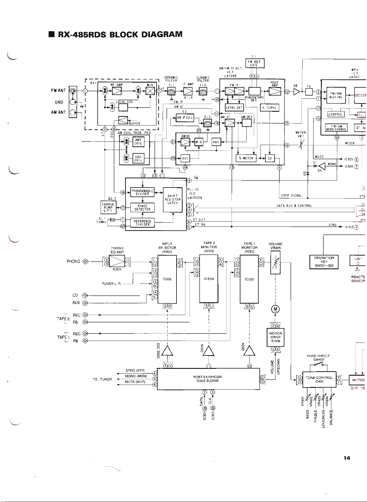
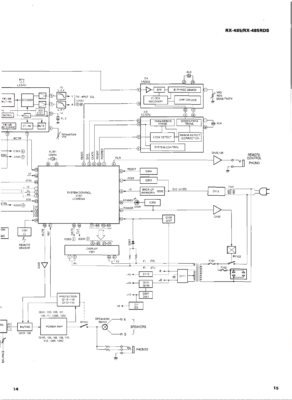
•
RX-485RDS
FM
ANT
GND
AM
ANT
BLOCK
DIAGRAM
CERAMIC
FILTER
Fi 1
AM/FM
I C 1
LA1266
IF
DET.
L.-"'T'""..,...
......
LM~U~T~E~
__
-+~IC505
t-";.,;;.;,;.""-!-
N
o
STOP
SIGNAL
DATA
BUSIiCONTROL
MP
I C3
LA3~
.•.
6
....
IC505
TAPE
TAPE
PHONO
r--
2
L
r--
1
L
GO
AUX
REG
PB
REG
PB
~
TUNERL,R
TO:TUNER
STRQ
MONO
MUTE
(STR)
(MON)
(MUT)
INPUT
SELECTOR
(4052)
r..::....:.....c..:..:::....-
TAPE
MONITOR
(4053)
I
~~
PORT
EXPANDER
IC505
9
II
I
I
I
I
I
I
I
I
/I
BU2040
---..
2
TAPE
1
MONITOR
(4053)
IC503
9 II
I
I
I
I
I
I
I
I
I
v
8~
10
VOLUME
VR405
I
I
I
I
I
I
I
I
®
~
2
10
MOTOR
DRIVE
IC506
PURE
DIRECT
SW401
---'S:<..,T'-"R""O_IC505
R
SE.
~
en
en
«
III
w
en
~
()
en
III
w
Z
W
z
a:
:3
0
~
«
::J
III
0
-J
14
Page 16
MPX
I C 3
lA3401
T5
l.P.
F
l]TOINPUT
IC502
R®®..---------------<
SEl.
RX-485/RX-485RDS
VR3
RDS
SENSITIVITY
REMOTE
CONTROL
PHONO
I;
REMOTE
SENSOR
<l)
a
('")
o
0101.103,105,107,
109, 111, 129A, 129C
POWER AMP
0102,104,106,108,110,
112, 130A, 130C
Icsos0
I
I
I
I
I
I
I
RY101
SPEAKERS
SW101
+5
A
l
SPEAKERS
J
B
0120
D107
S12 (+12S)
0122
u
z
<:
...J
<:
lD
14
mPHONES
15
Page 17
RX-485/RX-485RDS
•
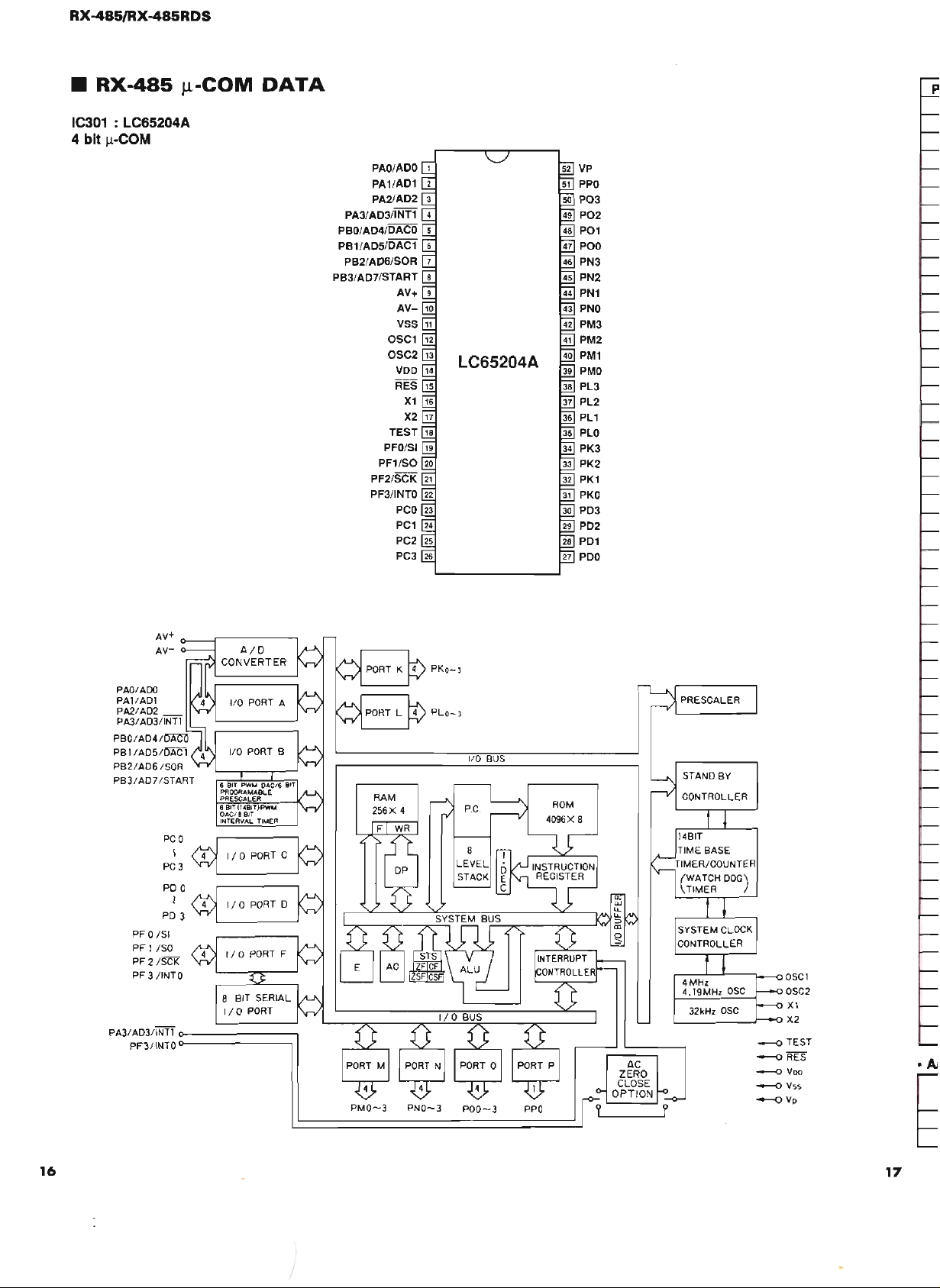
RX-485
Jl-COM
IC301 : LC65204A
4 bit
Il-COM
DATA
p
PAO/ADO 1
PA1/AD1
PA2/AD2
PA3/AD3/INT1
PBO/AD4/DACO 5
PB1/AD5/DAC1 6
PB2/AD6/S0R
PB31
AD7/START
AV+
AV-
VSS
OSC1
OSC2
VDD
RES
X1
X2
TEST
PFO/SI
PF1/S0
PF2/SCK
PF3/1NTO
PCO
PC1
PC2
PC3
4
7
11
21
LC65204A
VP
PPO
P03
P02
P01
POO
PN3
PN2
PN1
PNO
PM3
PM2
PM1
PMO
PL3
PL2
PL1
PLO
PK3
PK2
PK1
PKO
PD3
PD2
PD1
27
PDO
PAO/ADO
PAI/ADl
PA2/AD2 _
PAJ/AD3/INTI
PBO/AD4/0Aml
PB1/AD5/0ACi
PB2I
AD6 /SOR
PB3/AD7/START
PD 0
PD 3
PFO
lSI
PF
I ISO
PF
2 ISCK
PF
3 IINTO
PA3/AD3/INTl
PF3/INTO
I
0----------,
0---------,
PMO-3
PNO-3
110
POO-3
BUS
PPO
r--""O-"'
<--
..........
---,._.r.
-J""~-v
OSC
OSC2
Xl
X2
--<> TEST
--0
RES
--0
Voo
--0
Vss
--oVp
1
16
17
/
Page 18
Pin No.
1
2
3
4
5
6
7
8
9
10
11
12
13
14
15
16
17
18
19
20
21
22
23
24
25
26
27
28
29
30
31
32
33
34
35
36
37
38
39
40
41
42
43
44
45
46
47
48
49
50
51
52
Port
PAO
PA1
PA2
PA3
PBO
PB1
PB2
PB3
AV+
AV-
VSS
OSC1
OSC2
VDD
RES
X1
X2
TEST
PFO
PF1
PF2
PF3
PCO
PC1
PC2
PC3
PD~
PD1
PD2
PD3
PKO
PK1
PK2
PK3
PLO
PL1
PL2
PL3
PMO
PM1
PM2
PM3
PNO
PN1
PN2
PN3
POO
P01
P02
P03
PPO
Vp
At Reset
H
H
H
H
H
H
H
H
H
H
H
H
L
L
L
L
L
L
L
L
L
L
L
L
L
L
L
L
L
L
L
L
L
L
L
L
L
L
L
L
L
& Market detect
Model
Protection input
Tuner market input A1
Tuner market input A2
Power down detect
Signal meter input
Key input 1
Key input 2
+5V
GND
GND
4MHz (clock)
4MHz (clock)
+5V
RESET
VDD
OPEN
GND
Tuner STO in
Tuner STSG
Tuner ST in
Remote control
CE for LM7000
CL for LM7000
DA for LM7000
Mute out
Power on relay out
Phono remote out
Port Expander (Clock)
Port Expander (Data)
FL segment 1
FL
segment 2
FL segment 3
FL segment 4
FL
segment 5
FL
segment 6
FL
segment 7
FL
segment 8
FL
segment 9
FL
segment 10
FL segment
FL segment 12
FL digit 1
FL digit 2
FL digit 3
FL digit 4
FL digit 5
FL
digit 6
FL
digit 7
FL
digit 8
STBY LED out
FL,
Power supply
in
in
11
Function
(485G :
H,
385 not G :
Logic
L)
"-----
:ON
L
L:
down
H:ON
H:ON
H:ON
H:ON
H:ON
H:ON
H:ON
H:ON
H:ON
H:ON
H:ON
H:ON
H:ON
H:ON
H:ON
H:ON
H:ON
H:ON
H:ON
H:ON
H:ON
H:ON
H:ON
• AID INPUT PORT
No.
7
8
17
Name
KEY 1
KEY2
0
MEMO
POWER
1
EDIT
TAPE 2
KEY
PS
6
DOWN
2 3 4 5
MODE
TAPE 1 AUX TUNER CD PHONO
FM/AM
TU
DOWN TU UP
7 8
PS
UP
-
A-E
-
Page 19
•
RX-485RDS
IC301 : LC866024B-5512
8 bit /l-COM
Jl-COM
DATA
P10/S00
P11/S10/SBO
P121SCKO
P13/S01
P14/S11/SB1
P15/SCK1
P16/BUZ
P17/PWM
TEST1
RES
XT1
XT2
VSS
CF1
CF2
VDD
P80/ANO
P81/AN1
P82/AN2
P83/AN3
P70/INTO
P71/INT1
P721INT21T0IN
P73/INT31T01N
SOITO
S11T1
S21T2
S31T3
S41T4
S51T5
S61T6
S71T7
o
P07
P06
P05
P04
P03
P02
P01
POO
S29
S28
S27
S26
S25
S24
S23
S22
S21
S20
S19
S18
S17
S16
VP
VDDVPP
S151T15
S141T14
S131T13
S121T12
S111T11
S101T10
S91T9
S81T8
Pin
10
11
12
13
14
15
16
17
1
2
3
4
5
6
7
8
9
No.
Port
P10 CE7000
P11
P12
P13
P14 RDS DATA
P15 RDS
P16 RDS RESET
P17
TEST
RES
XT1
XT2
VSS VSS
CF1
CF2 OF2
VDD VDD
P80 TUKIN 1
Name
DATA7000
ClK7000
PHONO REM
ClK
RDSID
-
RESET
XT1
- -
OF1
I/O
0
0
0
0
0
-
-
-
-
-
-
I
I
I
I
I
Function
CE
for
lM7000
DATA for
CLOCK for
Player remote control (PLAY/CUT)
RDS DATA (lC7073)
RDS CLOCK (LC7073)
RDS RESET (LC7073)
RDS
N.C.
Reset
VCC
N.C.
GND
] Clock (12MHz)
+SV
Tuner keyin1
ID
(lA2232)
lM7000
lM7000
(ND)
18
Page 20
(
RX-485/RX-485RDS
Pin No.
18
19
20
21
22
23
24
25
26
27
28
29
30
31
32
33
34
35
36
37
38
39
40
41
42
43
44
45
46
47
48
49
50
51
52
53
54
55
56
57
58
59
60
61
62
63
64
Port
P81
P82
P83
P70
P71
P72
P73
SO
S1
82
83
S4
S5
S6
S7
S8
S9
S10
S11
S12
S13
814
S15
VDD VPP
VP
S16
S17
S18
S19
S20
S21
S22
S23
S24
825
826
S27
S28
S29
POO
P01
P02
P03
P04
P05
P06
P07
Name
TUKIN 2
AMP KIN
METER
POWER DOWN
RDS START
INITIAL
REMCON
MODEL
V3
11G
10G
9G
8G
7G
6G
5G
4G
3G
2G
1G
P1
P2
P3
VDD VPP
VP
P4
P5
P6
P7
P8
P9
P10
P11
P12
P13
P14
P15
P16
STANBY
POWER
MUTE
DATA2040
CLK 2040
PRT
IN
STEREO
81G
OUT
IN
SIG
1/0
0
0
0
0
0
0
0
0
0
0
0
0
0
0
0
0
0
0
0
0
0
Function
I
I
I
I
I
I
I
0
0
0
0
0
0
0
0
0
0
0
0
0
I
I
I
I
I
I
Tuner keyin2 (AID)
Amp key in (AID)
Tuner meter input
Power down detect
RDS SATRT (LC7073)
Model detect
Remote control
Model select (P72)
STBY LED select
FL digit
11
FL digit 10
FL
digit 9
FL digit 8
FL digit 7
FL digit 6
FL digit 5
FL digit 4
FL digit 3
FL
digit 2
FL digit 1
FL segment 1
FL segment 2
FL segment 3
VCC
-VEE
FL
segment 4
FL
segment 5
FL
segment 6
FL
segment 7
FL
segment 8
FL segment 9
FL segment 10
FL segment
FL segment 12
FL segment 13
FL
segment 14
FL
segment 15
FL segment 16
STBY LED OUT
Poweronrelay out
Mute
DATA for BU2040
CLOCK for BU2040
Protection
STEREO (TUNER)
STOP OUT (TUNER)
IF
Count (TUNER)
11
(SO,
(AID)
S1)
18
• AID INPUT PORT
No.
17
18
19
Name
TUKIN 1
TUKIN 2
AMPIN
0
MEMORY
PRESET
DOWN
POWER
KEY
1
EDIT MODE
PRESET
UP
PHONO CD TUNER
2
FM/AM
AlB/C/D/E AF
3
4 5 6
TUNING
DOWN
FREQ/PSI
PTY
LD
TUNING
UP
SHIFT
TAPE 1
-
ENTER
TAPE 2
19
Page 21
RX-486/RX-486RDS
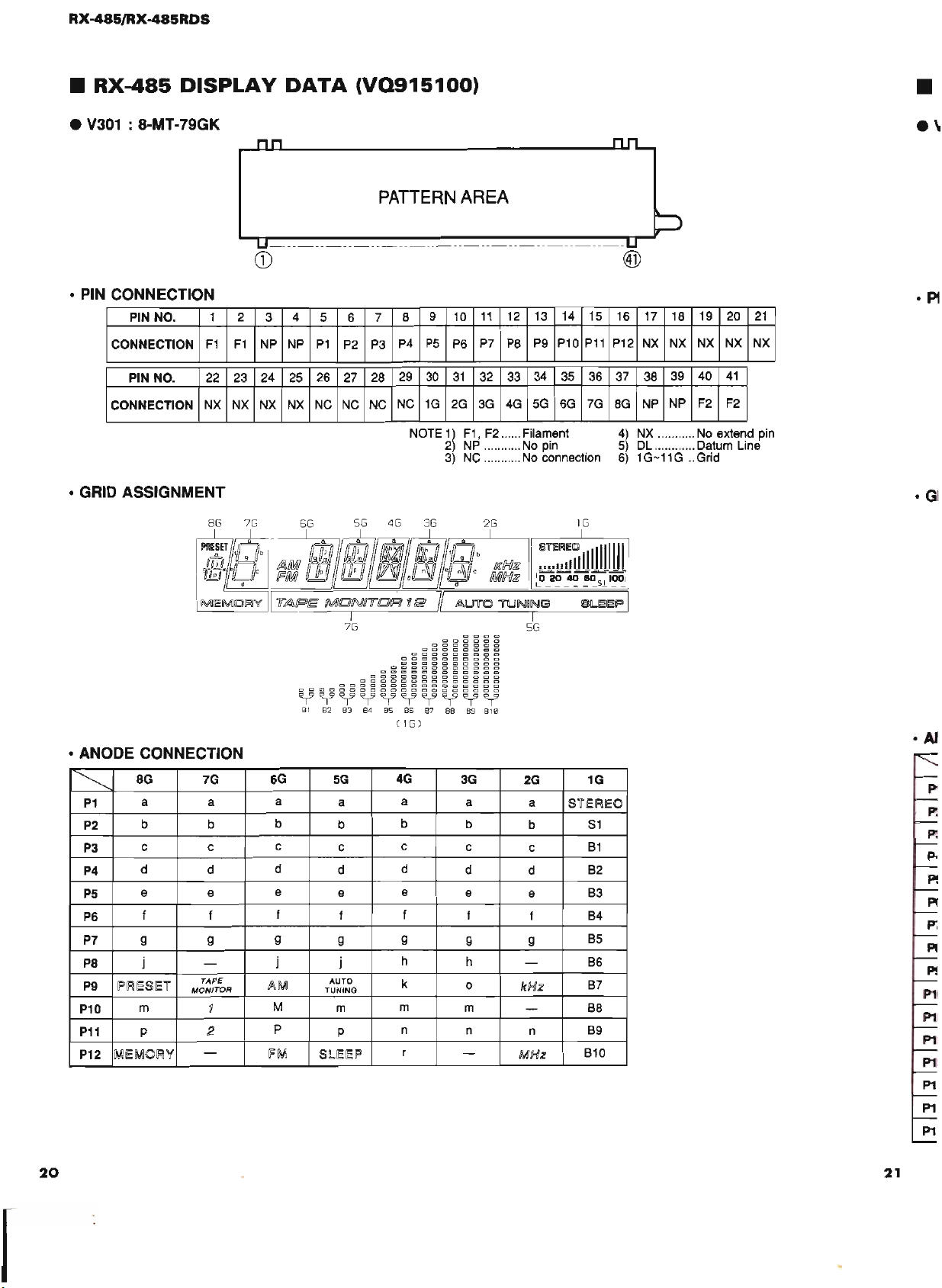
•
RX-485
•
V301
: 8·MT·79GK
DISPLAY
DATA
(VQ915100)
•
• PIN CONNECTION
PIN
NO.
CONNECTION
PIN
NO.
CONNECTION
1 2
F1
22
NX NX NX
• GRID ASSIGNMENT
BG
F1
23
7G
PATTERN
CD
4
3
NP
24
5
NP
P1
26
25
NC
NX
6G
~~yyyy~yy~
81
82
7 8
6
P2
P3
27
28 29
NC NC
5G 4G
0000000000000
00000000000000
83
84
000000000000
P4
NC
NOTE1)F1,
ocooooooo
0000000000
0000000000
00000000000
85 86
(
lG)
9
P5
30
1G
3G
00000000
87
0000000
AREA
10
P6
31
2G
2)
NP
3)
NC
COOO
000000
8889810
11
P7
32 33
4G
3G
F2
2G
12
P8
Filament
No
No
14
13
P9
P10
34
35
5G
6G
pin
connection
15
P11
36
7G
lG
SILIEIEIP I
17
16
P12
NX
37
38
8G
NP
4)
NX
5)
DL
6)
1G-11G..Grid
19
18
NX NX NX
NX
40
39
F2
NP
No
Datum
20
41
F2
extend
Line
.pt
21
pin
• ANODE CONNECTION
~
P1
P2
P3
P4
P5
P6
P7
P8
P9
P10
P11
P12
20
8G
a
b
c
d d d
e
f
9
j
PJRESIET
m
P
MEMORY
7G
a
b b
c c
e e
f
9 9
-
TAPE
MONITOR
1
2
-
6G
~M
M
fM
5G
a
a
b
c
d
e
f
j
f
9
j
AUTO
TUNING
m
P
P
SLEEP
4G
a
b
c
d
e
9
h
k
m
n
3G
a
b
c
d
e
f
f
9
h
0
m
n
r
-
2G
a
b
c
d
e
f
9
-
kHz
-
n
MHz
1G
STIEREO
81
B1
B2
B3
B4
B5
B6
B7
B8
B9
B10
p
P:
:p
21
Page 22
•
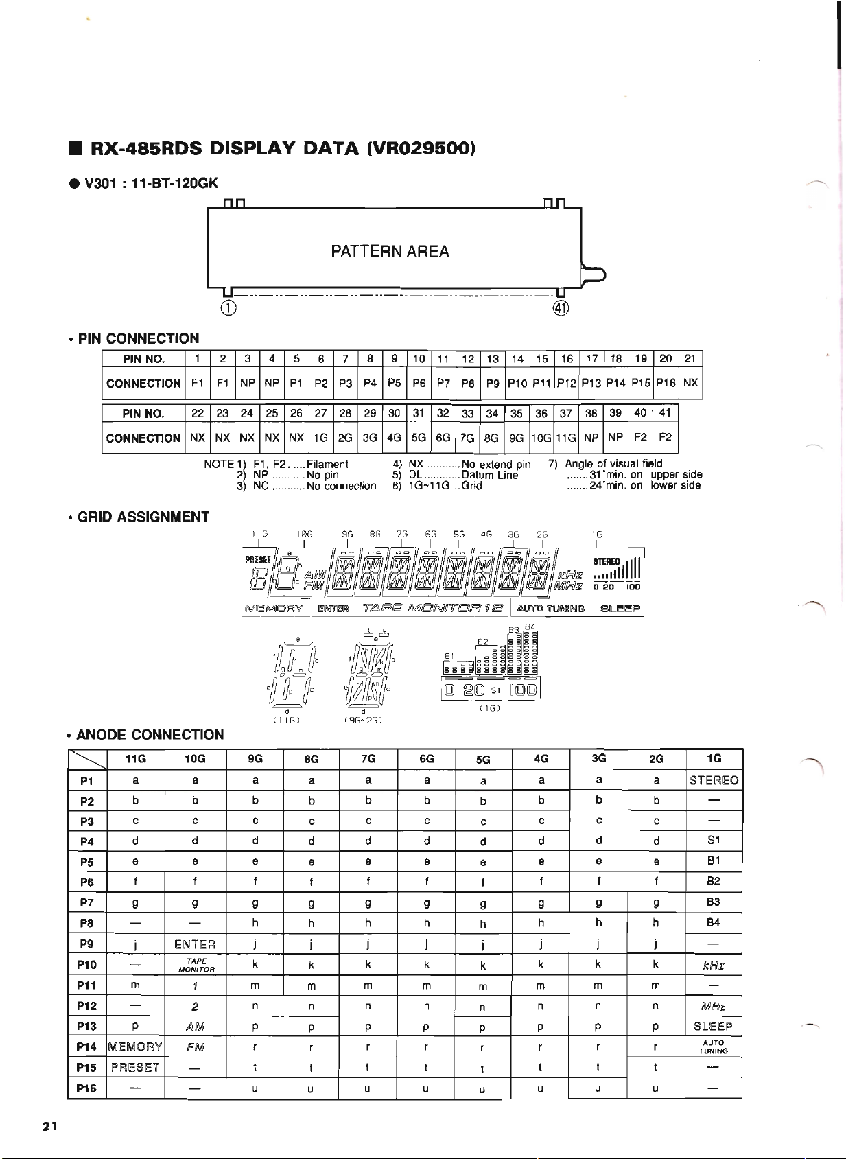
RX-485RDS
DISPLAY
DATA
(VR029500)
• V301 : 11-BT-120GK
• PIN CONNECTION
PIN NO.
CONNECTION
PIN NO.
CONNECTION
1
F1
22
NX NX
NOTE 1) F1, F2 Filament
• GRID ASSIGNMENT
• ANODE CONNECTION
~
P1
P2
P3
P4
P5
P6
P7
P8
P9
P10
P11
P12
P13
P14 MIEMORY
P15 PRESIET -
P16
11G 10G 9G
a
b b b
c
d d
e e e
f f f
a a
c c
9 9 9
-
j
-
m
-
p
-
rENTIER
TAPE
MONITOR
1
2
AM
FM
- -
CD
2 3 4
NP NP
F1
24
23
25
NX NX NX
2) NP No pin
3)
NC No connection
1 I G
'~J1b
"§£U'
d
(
l1G)
d
h
j
k
m
n
P
r
t
u
5
6
P1
P2
26
27 28
1G 2G 3G
10G
8G
a
b
c
d
e
f
9
h
j
k
m
n
P
r \
t
u
PATTERN
7
P4 P5
P3
29 30
9G
~u
'5.
tiff'
d
(9G~2G)
7G
a
b b
d
e
9
h h
k
m m
n
AREA
8 9 10
4G 5G
4)
5)
6)
8G 7G 6G 5G 4G 3G 2G
b
c
f
j j
11
P7
P6
31
32 33
6G
NX No extend pin
DL Datum Line
1G-11G..Grid
~ ~
~ltl!l~U
~~~=l
I
(Q)
6G
a
c
d
e
f
9
k
n
P P
r
t
u
r
t
u
@
12 13
P8
7G
g g g
~(Q)S1~
14 15 16
P11
P10
P9
34 35 36
8G 9G
82
~~g~II~~1
~ ~
10G
7)
.
~:~(,
~.~
:~
~.
(Q)(Q)I
(
lG)
5G
a
b
c
d
e
f
9
h
j
k
m
n
P
r
t
u
4G
a
b
c
d
e
f
9
h
j
k
m
n
P
r
t
u
d
e
h
k
n
P
u
c
f
j
r
20
41
21
1G
STERlEO
-
-
S1
81
82
83
84
-
kHz
-
MHz
SLEEP
AUTO
TUNING
-
-
19
18
17
P13 P14
P12
37 38
11G NP
Angle of visual field
.......31·min. on upper side
.......24·min. on lower side
P15 P16 NX
40
39
NP F2 F2
1G
~='IIIIII
020100
SIL/EIEIP
3G 2G
a a
b b
c
d
e
f
9 9
h
j
k
m m
n
P
r
t t
u
r--.
~
.,.--,
21
Page 23
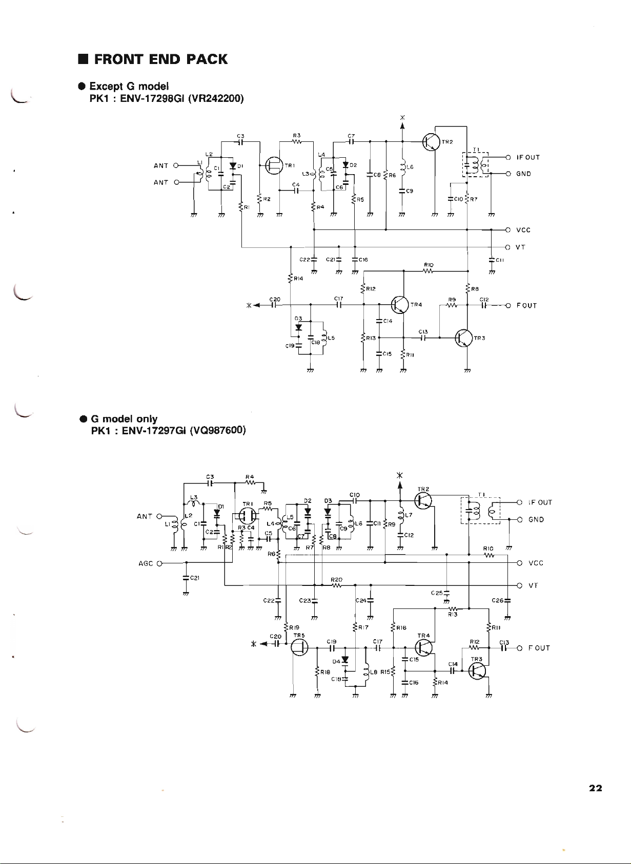
• FRONT
• Except G model
PK1
: ENV-17298GI (VR242200)
END
PACK
• G model only
PK1
: ENV-17297GI (VQ987600)
ANT
ANT
C3
L2
RI
;I(
~
R3
C20
t----+--~-__t
CI7
I------+-_----if-f
L5
TR2
C8
R5
I
RIO
T1
~R~~f
Clo
IFOUT
GND
r
vee
VT
lCIl
R8
TR3
CI2
1----0
FOUT
R9
L3
L1
ANTl
AGC
C21
r
C3
R4
*
Cl0
CII
C
C9
R.
L6
I
:::~::r
IF
GND
OUT
W
VCC
C22
r
C23
r
R20
C24
r
C25rl;
C26
RI3
RII
C'h
r
VT
F
OUT
22
Page 24
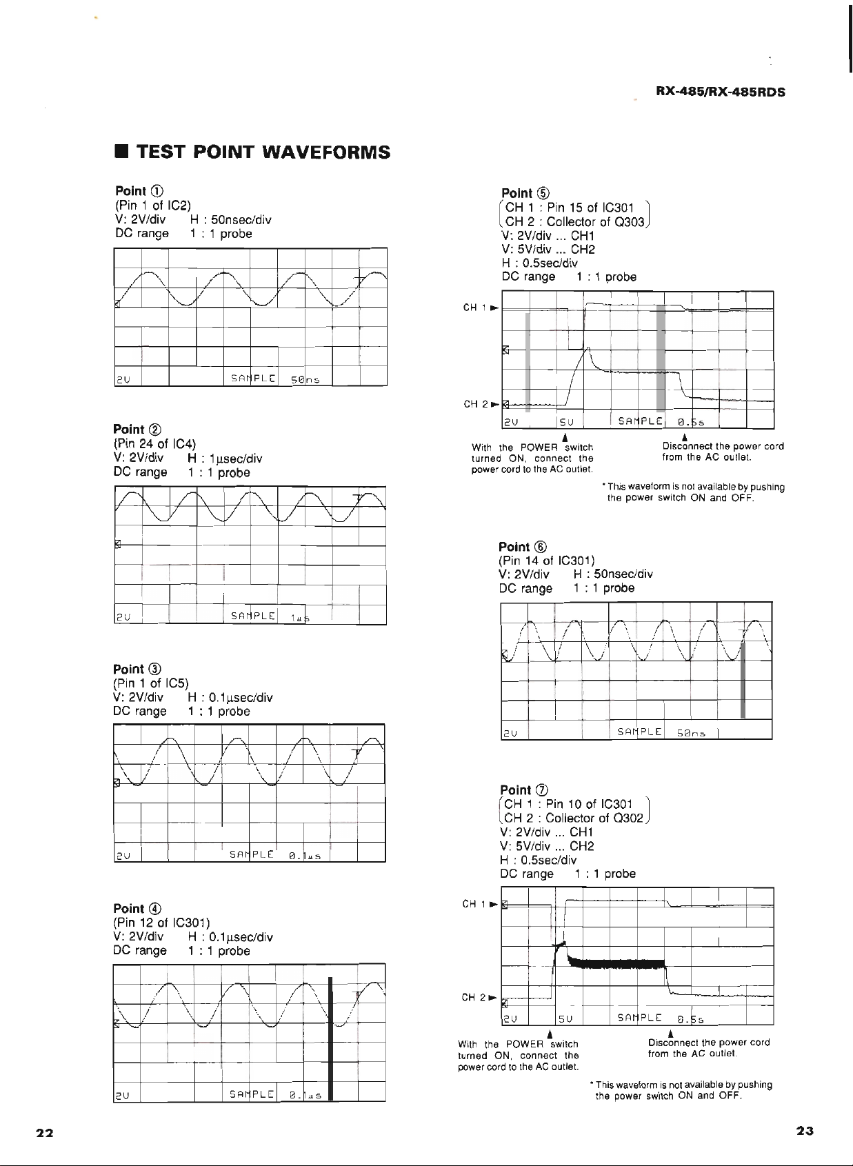
•
TEST
Point
CD
(Pin 1 of IC2)
V:
2V/div H : 50nsec/div
DC
range
---"
/
"if/
"
' /
POINT
1:
....
"-..,./
<
1 probe
//
""\
WAVEFORMS
/~
\
1"'-.-./"
'\
~
..-/
~~
/
CH
1
Point ®
CH1:Pin15of
[
CH
2 : Collector of 0303
V:
2V/div
V:
5V/div CH2
H : 0.5sec/div
DC
range
~
CH1
1:
IC301
1 probe
RX-485/RX-485RDS
J
2lJ
Point ®
(Pin24of IC4)
V:
2V/div H :
DC
range
~
1/
"'---
171
P'
2lJ
Point ®
(Pin 1 of IC5)
V:
2V/div H :O.1llsec/div
DC
range
r-.-.
/
!
bl
\,
l/
PI
2lJ
\
r
1:
1\
1:
\
1ll
ec/div
s
1 probe
l/
'"
1 probe
/"'\.
!
/
SM
S
A~
/
SA~
PLE
1'\
PLE
\
\
PLE
DI
""
58
ns
:71
CH
2~
2lJ
With the POWER switch
turned ON, connect the
power cord to the
\l/
-~
Point ®
(Pin14of IC301)
V:
2V/div H : 50nsec/div
DC
range
,
.'
~
\
l/
1.u
p
AC
/
5lJ
,
outlet.
"
/~
/
SA~
• This waveformisnot availablebypushing
the power switch
1:
1 probe
\
\...
PLE
8.
::>s
,
Disconnect the power cord
from the AC outlet.
ON
and OFF.
\
,
kJ/
SAHP
./r...
\
/
\
;
\.
\
8.
.uS
/'.
-fi
I
/
2lJ
Point (j)
CH
1 :
[
V:
V:
H : 0.5sec/div
DC
Pin10of
CH
2 : Collector of 0302
2V/div
5V/div
range
CH1
CH2
1:
IC301
1 probe
LEI581n
J
s
22
Point ®
(Pin12of IC301)
V:
2V/div H : 0.1Ilsec/div
DC
h.\
~
2lJ
range
1/
/1\\
/-I-"'
...
\.1
1:
1 probe
/ \
.I
\
SAt"jPLEI
0;;;;:;;
1/
7
8.lI.us
CH
1
~
""
l
1
,
v'
\1
7
\'i
;"
=
CH
2~
[;i'f
2lJ 5lJ
With the POWER switch
turned ON, connect the
power cord to the
AC
I
,
outlet.
SA~
• This waveformisnot availablebypushing
the power switch ON and OFF.
\
\....
PLE
Disconnect the power cord
from the
ps
8.
,
AC
outlet.
23
Page 25
I
PoCoBo
c
MAIN
( 1 )
A
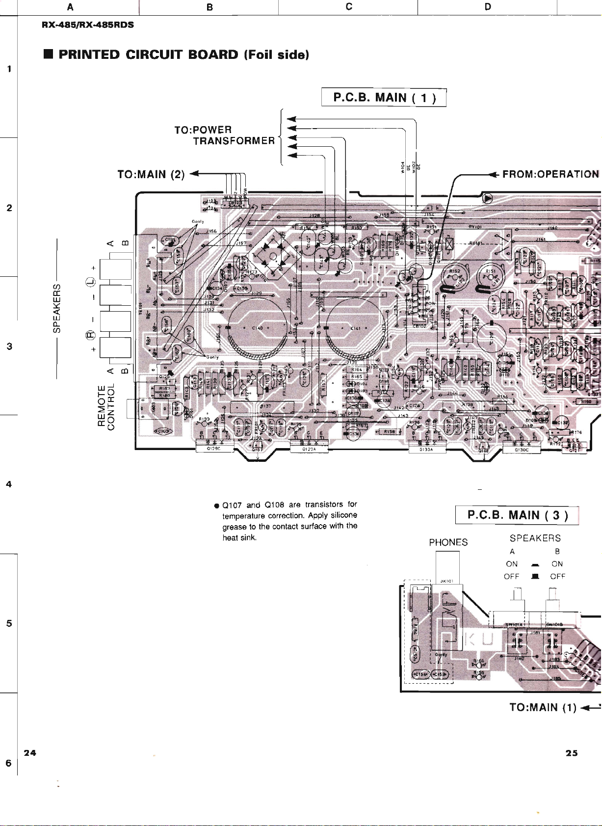
RX-485/RX-485RDS
•
PRINTED
1
CIRCUIT
TO:POWER J:
B
BOARD
TRANSFORMER l:
(Foil side)
...
~:=I--
-=:=----..,.==-----1
o
1
TO:MAIN (2)
2
+
C/)
a:
UJ
~
~
UJ
0-
C/)
g
.....
~-
~-~
FROM:OPERATIO
®
3
+
4
•
0107
and
0108
are transistors for
temperature correction. Apply silicone
grease to the contact surface with the
heat sink.
5
24
6
PHONES
PoCoBo
MAIN
( 3 )
SPEAKERS
A B
ON ON
OFF
•
OFF
TO:MAIN (1)
.....-.=
25
Page 26

]
IERATION ( 1 )
F
G
L
p.e.B. INPUT I
RS
ON
OFF
B
25
Page 27

A
•
PRINTED
1
CD
to
® :TEST POINT WAVEFORMS (See page 23)
2
CIRCUIT
B
BOARD
(Foil
side)
c D
SEPARATION
ADJ.
3
4
5
---TO:
6
OPEl
26
Page 28

_________
• RX-485
I P.C.B. TUNER
E -'-- F G H
RX-485/RX-485RDS
__
~
RX-485 RDS
P.C.B. TUNER
750
UNBAL. ANT
11------'1
GND
ANT
FM/AM
50kHz / 9kHz
100kHz / 10kHz
FREQUENCY
I
FM
I
AM
I
I
STEP
I
Ronly
I
)
~~~--l~TO
RATION ( 1 )
SIGNAL
METER
ADJ.
750
UNBAL.
MONAURAL
DISTORTION
ADJ.
(ANTENNA)
FM
ANT
GND
I
AM
ANT
I
27
Page 29

A
RX-485/RX-485RDS
B
c
D
• PRINTED
1
®
to
® :TEST POINT WAVEFORMS (See page
CIRCUIT
BOARD
(Foil
side)
23)
• RX-485
I P.C.B. OPERATION (
MEMORY EDIT MODE
TUNING
2
FM
/ AM
FROM : MAIN ( 1 )
3
• RX-485
4
I
p.e.B.
OPERATION ( 3 )
• RX-485
I P.C.B. OPERATION (
5
4)
1
.........
---
...
VOLUME
28
6
29
Page 30

J E F G
L.-
H
------lI_
~ATION
( 1 )
UDNESS
29
BALANCE
• RX-485
I P.C.B. OPERATION ( 2 )
TREBLE
BASS
.......
-.z
-4
o
3:
»
Page 31

A
B
c o
• PRINTED
1
®
to
(j) : TEST POINT WAVEFORMS (See page 23)
2
CIRCUIT
BOARD
(Foil
side)
• RX-485 RDS
I
PoCoBo
OPERA'
FROM:
M I
3
• RX-485 RDS
4
5
• RX-485 RDS I
I
PoCoBo
OPERATIQN (
p.e.B.
OPERATION ( 3 )
4)
I
r-----
....
VOLUME
30
6
Page 32

E
F
G
RX-485/RX-485RDS
H
J'---_
• RX-485 RDS
I
p.e.B.
OPERATION
FROM:
( 2 )
.....
INPUT
...
-I
o
3:
»
z
31
Page 33

A
RX-485/RX-485RDS
•
PRINTED
1
2
CIRCUIT
B
BOARD
e
I
(Foil
u,
C
PoCoBo
side)
models
MAIN
( 2 )
c o
,...
-
-
z
ct
~
~
o
0:
u..
3
model
I
PoCoBo
4
5
MAIN
( 2 )
,...
-
-
z
ct
~
~
TO:POWER
TRANSFORMER
.......
~~~,,~
o
0:
u..
AC
OUTLETS
PJ
~-
e G
eR
32
6
33
Page 34

JL---
E
--.l..
~F
G _
T""
-
-
z
________
H
---1
__
• R model
[P.C.B.
!l!:i
~
MAIN ( 2 )
:11191
-
TO:AC
'AI
106
GY
T""
-
-
Z
<t
~
----,--------.----'--~
Will
BR
~
o
II:
u..
TO:POWER
OUTLET
•.
R model
I P.C.B. MAIN ( 4 )
y~
__
TRANSFORMER
..-J
110V
120V
1-2/5-6
2-3/6-7
3-4/7-8
4-5/8-1
33
Page 35

...z
08
3
1710KHz
\
I-<z
AM
SENSITIVITY
ADJ.
_______
4
5
L.
P.
6
F.
PLL
L _
PK1
: ENV-17298GI (VR242200)
7
C3
L2
ANT
ANT
R3
IFOUT
GND
RI
vee
VT
RIO
8
C20
*.....-.
t---+--..,.---I
L5
CI7
It---+-
R12
.......
--+£
......
I\fr--+----i
TR3
CI2
t---o
F 0 UT
Page 36

A
•
SCHEMATIC
DIAGRAM
B
(RX-485
c
TUNER)
D
1
CAPACITOR
REMARKS
!-,-N;,.::O--=:-M
A:..;..:R..:.;.K:...r-=-E.=.L
®
NO
I---::O~-+~P
TANTALUM
MARK
CERAMIC
@
CERAMIC
@
POLYESTER
O~L::....:Y~S...:...T..:....:Y
CD
IHCA
®
POL
•
SEMI
PARTS
E=-C,,"-,T,-,-R;,.::O-=.L-,-YT.:....:I=-=C,----=C:.:..;A-,-P-,-A
CAPACITOR
TUBULAR
R-':.::E:..:..:N.=:E-,F,--,I,-=L,-,-,H~C
CAPACITOR
YPROPYLENE
CONDUCTIVE
NAME
CAPACITOR
CAPACITOR
FILM
CAPACITOR
FILM
CERAMIC
C=...;I:....;T-"D..:.;.R
~A
P-::.A,-"C~I
CAPACITOR
---;
~T
O~R':""-_--l
CAPACITOR
RESISTOR
a
H
REMARKS
NO
MARK
IZl
!::,
P:.
~
~
0
~
•
CARBON
CARBON
METAL
METAL
METAL
FIRE
CEMENT
SEMI
CHIP
PARTS
FILM
FILM
OXIDE
FILM
RESISTOR
PLATE
PROOF
CARBON
MOLDED
VARIABLE
RESISTOR
NAME
RESISTOR
RESISTOR
FILM
RESISTOR
RESISTOR
RESISTOR
RESIST
FILM
(P=5)
(P=10)
RESISTOR
OR
NO
('J)..,..
(U)···
(C)..•
(A)
....
(G)..•·•
(6)
....
(R)..•
(P)..•··
=
..
..
•
·
..
2
I----------------------=~~------D~=~~-
75Q
DISTORTION
ADJ.
(ANTENNA)
u
22
uH
BALANCE
ADJ.
(FRONT)
AM
3
FM
87.5MHz
98.IMHz
I08MHz
AM
530KHz
1080KHz
(
1710KHz
1.7V
4.2V
8.4V
IAV)
4.9V
7.8V
AM
SENSITIVITY
ADJ.
FM
4
l"1
u,;~
.".
0
6
~
c.J
0
:I:
(\J
~
...J~
""
%
.".0
5
L.
P.
6
F.
PLL
'"
Page 37

F
I
)
j
a:
~
!i!
-
OlO
06
.
06
o)0
C333D
~
(0.6)
47K
4
nc2~--l
I
-
..
I
'I
IA/S/T I
sWld
S~
R44
lOOK
~r
.
~
I
-
'I
/1OlO
I;::::
/STSIG
~
CE7DOO
c::;
elK
I:::::
DATA
c:::
STOUT
I:::::
STAll
h
MmR~
+12V
I;::::
52418
1
155133
155176
TO
INPUT
P36
B
-~
--
--
REGULATOR
-
--
-
--
SIGNAL
M~TER
ADJ.
-
---
-
--
-
--
-
--
-
--
-
---
-
--
--'
I
PIN CONNECTION DIAGRAMOFTRANSISTORS, DIODES AND ICS.
2$~30~,S'B
2SA1317 •
E~
C
B
S.
~~g~~J~B.
C)
~
C
B
lSSl33
HZS6C2TD
g
Cathode
Anode
LM7000N
~"
1
L.A3401
22
~"
1
LA1266
~,
2.
1
Page 38

___
----L
E
...l-
F
G
H
--.JL
CE
0apanese
U. S. A
Canadian
Austra1ian
European
British
Ge
nera1mode
RP
model
model
model
mode
model
mode
mode
1
1
1
1
----------------------1
><
~
:::
,..----------l----------,
O(
0 J v
;;C;
~~
~
-
,
0(0122.
~
2.7
MPX
R32
~
1
2 PKI VR24220 VR24220 VR24220
3
4
5
6
7
C21
R34
B
9 J51
10
R48
11
T3
12
R35
13
C36·37
14
A36.37
15
SWl
16 J61
17
u· C
100P
10K
0 0 0
X X
X X
22K
6BOP
lOOK
X VF54120
X X
Interchangeable
Mark
Reference
01.2
l!
R
lOOP lOOP
10K
22K
680P
lOOK
PartsatManufacture-Stage
Parts
Number
A
10K
X
X
221<
470P
lOOK
X
X
Parts
HSS104
156133
156176
Name
--+--+-I---+-++------::>I"SI
l"'"
GNAL
Mf:TER
ADJ
.
t
-
1'1'
I
'I
010
o10 C3330 (RIS/TI
~
4
.6
47K
(0.61
06
sWld
sf5l
R44
lOOK
~r
.
Ij
I
~CB4
.~
'12
I"""
1ST
1;2
MUTE~
1101O
I;::::
TO
INPUT
I;::::
~
~
I;::::
P36
B
5241B
~
CE7DOD
elK
DATA
t12V
I
.Il15[V]
.4
11.1(III
'I~}
(6.1)
I
~~
a:.-4
>----
~;~(~~~
...
~010
REGULATOR
I
~
i!(j
N
Cl
Rl
:r
7"
Page 39

a04
il33
il76
IC3 : LA3401
MPX
ILl
...J
<l
U
U ~
o
I~
: LA2232
Decoder
•
Point
CD
(Pin
1 of
IC2)
V:
2V/div H : 50nsec/div
DC
6U1=
~/
2U
range
.......
/
0.0
1:
1 probe
TRIP1=2
~U
,
"\
'\
"",-"
~,
/'
/
SAt
.1U
\~
PLE
//"""
50
6T=1
~
ns
'"
~
.0n~
ISAV
L/'.
,~
: LC7073
; Converter & Contn
..
All
voltage are measured with a
..
Components having special characteristics are marked
and
must be replaced with parts having specifications equal
to those originally installed.
..
Schematic diagram is subjecttochange without notice.
101lAO.lDC
electric volt meter.
ib
34
iv
./
_E
I
//
"\.
50
ns
~
-y
/·1
Page 40

______________________________
4220
:acture-Stage
3rts
Name
;104
5133
Si76
IC1
: LA1266
AM/FM IF
IC2 : LM7000N
PLL Controller
SYC
7
XIN
I}----~
XOUT
J K
RX-485/RX-485RDS
FM-IN
I
9
REG.
ITO
22PINI
----
: LA1266
FM IF
: LA3401
II
AM
IF
--..JI_
ILl
U
d
IC3 : LA3401
MPX
Point
CD
(Pin1of
V:
DC range
~V1=
IC2)
2V/div H : 50nsec/div
1:
1 probe
8.8
~V
TRI
P
5}------{
~
o
1=~
.1V
~T=
~c;28!'>
I~
: LA2232
» Decoder
~/
2V
I.-'\.
./
\.",,--,,1
/".
I'\.
\~
//
f'\
-v----
/.
: LC7073
»Converter &
'"
SAt
PLE
58
ns
Page 41

3
I
_:
4
/
ru
S METER
...J
~(\J
~l~
I
~
0
~J.g
u,;r"
5
L-
-1f--
l'J1h~::!;:
-"'~a:.,;
(~:~)
0(0)
R13
~
2,2101
R15
2.2K
l8Iy
~~:~
,
L.
Q2(
Q3(O:6)
C3330lRlSITl
G3330lRIs/TJ
p,
F.
,JOil
...
~
1/50
1.1)
fil
18
0.1(1.8
-1i---=2.::::.8C!.:(Q~F.:;:MO~5~G
~1P-~~
<:;tiJ
~
R22
10K
,,,
(0)
~
AMIF
0,1(0)
=--c
FMIF;g:I-'-FM..:..:M....::0'-'!(5::,::
AMOSC
':l
R<D~)
'<t
3"
tot5~T~OU~T",;;5""'.0.,.(5"",O~)'------l-f___;
~~
,,±....::::
<:;I
..
1r11"'0~(QC!.)
1~(1.1
~
..
<D
C\J"'p'0~(Q'-!.)---------'
20(0;;;
B
(\JI-'S~T~R<l~OC!.:(Q"-!l
1.4(1
~LZJ.7)
xb~
7,
214Hz
en:r:
<:;I~
<Xl:r:
~I~
PLL
..
GLO(O)
SIGNAL
ADJ
~
x: I
C!
~
Ic:....)
+-------+'
__I1
I i
-=
-+:+
-= -=
-;-;-=+f::
-= -=-= -=
-1(_
I
+-
__
+5V
D400[E,F
~_~9'E9E
'"
(6.01
~
~~f8
~
~
'-'
to
'1
;r
~-r-"':-
r'~
~_--.J
J
6.0
~ ~
~
0
~~~
ffi
Q,j~~
c.J C
en
:l:
r
I
6
77
REGULATOR
L _
PK1
: ENV·17297GI (VQ987600)
7
IF
OUT
trf
:::~::r
GND
.H1"r
vee
R20
C25;J;
8
RI3
C26
r
VT
FOUT
PIN
CONNECTION
2SC3330 (R. S. D
2SA1317 (R, S. T)
DIA
35
Page 42

A
B
c
D
RX-485/RX-485RDS
•
SCHEMATIC
DIAGRAM
(RX-485RDS
TUNER)
1
CAPACITOR
REMARKS
f-'N.:..::O'-..,:,:.M
~A
R,,-,K"4-=E.=.L::..E
®
NO
I---=O=---I~P~O::..L
TANTALUM
MARK
CERAMIC
@
CERAMIC
@
POL
<D
MICA
®
POLYPROPYLENE
•
SEMICONOUCTIVE
PARTS
C::..;T,-,-R:..::::O.=.L..:...YT.:....:I"-"C,---,,C..::..:A-,--P
YESTER
Y~S~T....:-Y.:...:.R=..:E
CAPACITOR
NAME
A,-,-,C=...::I,-,T...=.O-,-,-R
CAPACITOR
CAPACITOR
TUBULAR
FILM
CAPAC
N~E,--,-F~I
=..:L
M~C~A,-,-P~A~C
FILM
CERAMIC
---~
CAPACITOR
ITOR
~IT~O~R,--_~
CAPACITOR
CAPACITOR
-a
H
RESISTOR
REMARKS
NO
MARK
1ZI
6
A
~
~
0
~
II
CARBON
CARBON
METAL
METAL
METAL
FIRE
PROOF
CEMENT
SEMI
VARIABLE
CHIP
RESISTOR
PARTS
FILM
FILM
OXIDE
FILM
PLATE
MOLDED
NAME
RESISTOR
RESISTOR
FILM
RESISTOR
RESISTOR
CARBON
RESISTOR
RESISTOR
RESISTOR
FILM
Ip=51
(P=10)
RESISTOR
NOTICE
(-.J).....
(u)..··· u. s. A
(C).....
(A)·
(G).....
(B)..•.•
(R)
(P)..··•
-.Japanese
Canadia
.. ·•
Austra
Europea-
Brit'
....·Genera:'
RP
::c:
s-
e:"
2
3
\
R4
lOOK
IL
4
II
/
SIGNAL
METER
ADJ,
~l§llr-+----+--+------l---+------2
c..J
-
a.
g
0,1(0) FMIF
AMOSC
~~
~t<J
"±..'::::
c:;I"
gO<O
1.4(1
en:I:
C:;I~
a
(0)
[""'"""""""""
~
g:
~
Rcn~)
~
3"
1
....
r.:;:
9
cn"'rn""O...,,(O:.l..)
~
8NI-"S~TRG=0l"'<O'.L)
~
FMO(5.1)
""
C!
£
I
I
t<JtS~TOU~T-""5,"10~(5""',O.!-)
11lP'-0~10..:...)
~
CL
0<0>
---ttr-;:~t-;-;-;;t;;;;tjt~
__l111
-----'
-+-
__
~iLZll.7)
XbP
7,
2MHz
CD:I:
~~~
PLL
~
G.;,r~AMIF
5
'--
t-_-=-
~1h~;:
~
-~~a: r,j
R15
22K
.
RD
2.2'"
...
fil
1/50
0,1(1,8
-+-£2'~8~(0~FM~O~SC:
"llfl-
C:;fJ
~
.--+---+-,;'\0';':-",,-,-(1.
IR\~~
~:~
"Oil
(~'~)
,
(02
0101
10:6)
~
m
~~330IR/S/T)
L.
P.
(1.1)
C3330lAlsiTl
F.
A22
10K
117
I~
I!
I;,
I,!
~i
1--
~----=
6
7"
REGULATOR
Page 43

~
~
TPl
h5
i,!2
[fI
~~
O~
TP2
-
-+---~---'
r~
,
C
64
IrU
U
Er.
-;-;;--v
-~
1ST
52
HUTE
;::::
/I«)N()
-v
TO
418
II'PJT
P36
D
TO
OPERA
P38
o
/STSIG
;;
CElOOO
.0
elK
0
DATA
STOUT
g
~n
HETER
;::;
+12V
;::
52
I
I
IRDSRES
1~B6
ClK70 h
OI70
..---------RO--S",..ST::-i{P
,..----t--==:-i{h
~_+-_RO_S_ID-t<~
I~
i¥CFF11
THIN
IC4:
LA2232
RDS
Decoder
IN
PUT
(1)
77
lEGULATOR
_________________________________
---J
Point
CD
(Pin 1 of IC2)
V:
2V/div H : 50nsec/div
DC
i?[/
range
-,
/
1:
1 probe
'\
\''''-''
1',
/
/
IC5 : LC7073
RDS
Converter
//""
t'-.....••/
'"
'\
& ContJ'l
~
,V
/'
tiN
CONNECTION DIAGRAM OF TRANSISTORS, DIODES AND ICS.
2SC3330
m·
2SA1317 .
E~
C
s'B
S.
B
2SC535lA.
2SD400E.F)
~
C
s
B. C)
155133
HZS6C2TD
g
cathode
LC7073 LM7000N
Anode
,~,
1
~
1 1
LA3401
..
~"
LA1266
LA2232
~,
24
1
2U
SA~
PLE
50
ns
Page 44

IOTICE
))
))
:;
)
~
)
....•
:;).....
3)·····
::1)
•••••
:J)
•.•••
L
-.Japanese
U.S.A
Canad
ian
Australian
European
British
General
RP
model
model
mode
mode
mode
model
model
=-E
1
1
model
1
----------------------1
~
""
C'1
0
a:
""'r----------f-------
-----l
Interchangeable
Reference
Mark
't
01· 2
----=-F
PartsatManufacture-Stage
Parts
Number
Parts
Name
HSSl04
155133
155176
.L-
G
----l
H L
IC1
: LA1266
AM/FM IF
IC3 : LA3401
MPX
-+----------'
r~
2.
21's.
3150
MPX-19KHz
SEPARATION
ADJ.
./'
8114
....
0
lOOK
~r
a:
;:
MUTEh
/STSIG
CE7000
elK
DATA
STOUT
STRll
~
~
I~
c:::;
~
c;
TO
~~
52418
I
I
lAOS'" l"
CLK70
I~
DIlO
I;:::;
l¥CFFH
I
I
TO
.....------R::::D-=SS::-:T:--i\~
.....-_-+
__
R_D_SI_0---K.~
INPUT
P36
o
OPERATIClN
o
P38
IC4 : LA2232
RDS Decoder
IN
PUT
111
7"
~EGULATOR
I
I
I
I
I
I
IC5 : LC7073
RDS Converter
&
ContJ'
I
Page 45

:
LA2232
Decoder
20
17
...._-'--:--00
I I
L J
l-------=::::::;:=D-----~
AND
DATA
i
I
I
I
I
I
I
I
I
I
I
I
16
115
SK-ADJ
ROS-ID
1.-
:
LC7073
1
; Converter & Controller
ascI
OSC2
VSS3
CLOCK
DATA
RECEIVE
v
//""
1\
/
-~
/
'"
1_
~
OUT
OUT
Point ®
(Pin 24ofIC4)
V:
DC range
L'
~
po
-ll-~
DATA
IN
CLOCK
IN
DK-ID
-13--'
1-
--------------------
14
SK-ID
1-1-1-1--
VOO
VSSI
VSS2
VSS3
2V/div H : 1llsec/div
1:
1 probe
/r'\
~/
V
/
""'\
'"
CORR.
\
J
SEL
ERROR
LI'\
CORRECTION
OSC2
-~
\l/
L.-
1
ascI
D.S.CONTROL
__
~
DATA
.....
.......
----+----0
t----+--0-;-00
RES
CL,
ED,
--+----4I
SEL
CLOCK
DATA
START
RECEIVE
Point @
(Pin 1ofIC5)
V:
2V/div H : O.1Ilsec/div
DC range
1:
1 probe
r-,.
!
\
/
\
t;>,\,
/
\
!
/
"'"
.r'\.
OUT
OUT
L"",
\
\
\.
-
\
!
\
/
\
/'.
_./
I
_E
50
ns
2U
SAt
PLE
1.uj:.
..
All
voltage
..
Components
and
mustbereplaced
to
those
..
Schematic
2U
are
measured
having
special
originally
installed.
diagramissubjecttochange
SAt
witha10MQIDC
characteristics
with
parts
having
PLE
specifications
without
0.
.uS
electric
are
volt
marked
notice.
meter.
Lb
equal
Page 46

____
....l....-
........L.... J
---l-
K
--L-
L L
: LA1266
FM
IF
: LA3401
FM-IN
IC2 : LM7000N
PLL Controller
I
SYC
7
9
REG.
ITO
22PINJ
XIN
XOUT
I)----~
II
AM
IF
ILl
U
d
~
o
o
a::
l-
en
I~
: LA2232
j Decoder
'-------
: LC7073
) Converter
------9-
&Controller
",:-,,---ol-
1
-;-
-ll-~
-
o.4~JU__I__~~======::t==:::;====:::=:~~1
[-OR
I------=:::;::=t::>-----+-o
-13--'
1-
----------------------
SK-ID
14
CORR.
SEL
ERROR
CORRECTION
D.S.CONTROL
OK-ID
_-"---'--00
"
~
17
DATA
16
115
SK-ADJ.
ADS-ID
DATA
CLOCK
DATA
IN
IN
OUT
CLOCX
Page 47

-,~~
""
(g;
m
'"
3
I
1
/
I
1
-=-..--
-,
-_.3
IN
IT
Is
,
i.X
R544
,CTOR
R546
470
~5
..
70
-
~~
I'"'
v
S
J
~
_.:..
v
§
~
B:Qgj
aJ~
~
~~
~
a::
B
_ 0
~""
~ ~
B
u
~~
~ ~
~ ~
~-
~~
.
~
I
0
""
C\J
C\J
1'-
N
,
,
'"
~o
~6
-
°l~
1-
1-1-
o 0
~I
o 0
15 14 13 121110 9
1
li5~24U~0~05~CB
q
::1.
I'
0
0
~I
0
"0
TAPE 1
o 0502
~~
:t:}l
_____
o
OTC144ES
-
-I""
1 •
'Z
-~- .
I
~
-~.
-
:-:::1
MONITOR
-
o
0\
cD
16 15 141312 11 10
IC503 UP040536C
12345676
ollo
:11
II
i
I
'!
.j
N
I
I
-,
"""
-
,
JI
<Ii
o 0 0
~
6 15 14 13 12 11109
4
4
r1
liS03
°iO
~
.~
I
0 0
01;;;
:1
~Io
o
H~j048.6l2
8.10503
~r:r:
tg'0~05,BC6
00
~Io
-8.5
HSS1'04
C-~5~
8.1 HS;>j04
"2
;;
§t
;;
~
u
&,2
D~~7
-8.7
O·
1
0'502
" c
v 0
" c
v
~
o c
~
4.7
8.6
a
~P;
~~
I
~p;
~~
I
A550
3.31<
0051
3·
3K
TAPE 2
I
MONITOR
_8sJ3
~
CD
~
4
-:;
AUX
r0'
.'-'
-:;
I
PB
PJ502.
5
TAPE1
l
I
PJ503
6
TAPE2
l
REC
PB
PEe
~
-:;
~
~0
!
1.....0
~
I
[l.
330
-~~
C\J
~~~5
330'"
R516
8pJ]
330
~~
[l.
C\J
~~~
330
'"
R520
fl521
jjo
~C\J
[l.
'"
33O~~~
R524
8~?5
330
~
'"
330
~
R526
R527
jjO
~
N
~r~x
330
C\J
R530
8531
330
~
C\J
[l.~
330
~~
R532
3~
L _
7
8
PIN CONNECTION DIAGRAM OF TRANSISTORS, DIODES AND ICS.
2SD438
(E,
F)
~
C
s
DTCl44E5
~
155133
HZS5C2TD
HZSl2A2TD
HZS9B2TD
~
B
Calhode
NJM2068L-D
Anode
~
LBl641
~"
BU2040
,~8
IlPD4052BC
jlPD4053BC
,~8
1
1
Page 48

A
•
SCHEMATIC
B
DIAGRAM
(INPUT)
/
c
D
1
1----------------------
I
I
2
}t--...-:IIV5r.>
-:.; 2.
PHONO
Wv~
).}-j1--+.:f:J
3
,/
PJ501
'
850
........
2k
_
~c:Q.~~~
V>~N
-
~~~~~
V>
~
[if
2
2K
Vi:15QC-.
-+--..------lY
8
B
.8513
A516
-~----J1r-·+I----
~a:~
~~
~
PHONO
AMP
50
C~~
60
1C50
....
~4
I
;.~I1~~K5
~
a:
220/'I 0
al
..
"--'j~~
9l,O,OP
al
2294I 0
C508
'-!:!J,8
2
3 0
0
@c5W
R505
}C50
....-
6-
i!l"
EO
REGULATOR
1·
9.1
0 7
NJH2068LD
~
g
R~;35
a:
...
O·
3
~~3
2.2/50
2K
1ret'526
,~21<--+--,I;;w.:..OOt<--.
R536
NJH2066LD
o I
9.9
INPUT
~o
0
~6
15 14 13 12
~
1~5~24utD~05~CB
0
10 C 01--.:>;110
I .
I~!:'--I--+--+_-----'
~a:~
!ti
"'"
2.~50
C527
SEl
000
;;;;10
11
~I
:;:;.
5
~~
FeTOR
10 9
0
'-I-----t--r---,
R543
1.2K
R544
8546
470
s
-
o Q502 I
~~--I_;;
:EJ
_'
o
DTCI44ES
1
1 _
-'
~
I
I
- -
R520
TAPE
II
MONITOR
1
II
-
0)
000000)
161514
13
12 11
10
1
PJ502
5
TAPE1
R524
~
330 u
8526
R527
II
III
ii'
I~5~34tg'D~D51BC6
0000100
-,.-
i
Ii
II
II
+----+-----'I-+----=to)
PJ503
TAPE2
6
8530
~~1
~
Q.
.........__.....
C\J
~~
ru
~
::::.
+-
I
--r-,o
0 0
16 1514131211
1
I~5~44tg'0~D5,BCBI~~~~~
o 0 0 0
TAPE
MONITOR
9
~
8.1 H5fj04
...
~
/,2 0502
Hspj048.6l2
8.10503
r-=
til
o~
[':ai
J
10
91
J)
0
a:Jy--+-+T-HS-lS*ID-4~.:.:.....--+--3-?;J.'*'3I<~---
.....
_..._~....
-8.5
~I~~
r-:tf
_
/,2
D~~7
0·1
~~
u
~0~
u
~c~
8.7
--
J
8.6
a 3.31<
~i
0 c
....
~
~1
2
Page 49

CONTROL
I G503
i\
-
-10
~-
_:
ITC144ES
_
~G5.9'L
I "'-I' 10
:
eJ·
"0
-
OTC144E~
I
8.1
G505 I
:(~-
I I
7i
- - -
OTCI4J1ES
~~
-
~
r
VIII
C546 I
~~~P+_-_"_i0
1--_----'0"-1
~
1 P ° m
'--ir---.--t-----'0'-i....
t--+-_+-_--::;.3.'-'1<~
'--+--I--
__
-II--
- - I°
L---4-4-----I-----4--+--~_+-------_+__+
_I
~-+--+-__+---""2'_'_i.6
O,.--;.rm
4.7
C\l~~
7
~~~-
~_Ll1
(TJ~b
u
3.2
:::
3.2
"":r-:;...O
I'-~
°
~~
0
!If
~
~
117
-,
I£T
'12
STO
OAT
5TG
eLK
5T
OAT
CE
CLK
G
55
"A
;:;
;::
;:::
~
~
~
~
~
~
~
~
I
I
°
~ATIONIIJ
P37
~ORB
P38
Interchangeable
Hark
H
~2
Reference
Q501
0502. 503. 507
Parts
Parts
MOTOR DRIVE
,L..--
__
---1t--
__
R_O_-K
r~:JIB503
E
~==;;;::;:;;;::;:======--S;:=:;;;"""'~=;':;;;;;;;;;:;;;;~~-~+=~~~~~~~~?""::;;;::<t~;;;::;:;;;::;:::;;;::::;;;::::;;;::~;;;;;:;:'-""'+---=::;"',.-f---:+r;1"5-i<~
_ _
....-+--+-
....-__.l---1.L..-
-
0
0-t-
+-·
1
I~50~
1
2~~
I
O~.I·~N~ ~ID~I
°loTlB
LB1641 I I
1.4
5 6 7 8 9
'" '" '" '"
lR
l£~
I!
O,OL-
101
~I
-++-
__
_+_-'
-+-_---,,-,..,...15_-i{1~~1
--t-_---:"-=I---:-;h
LO;:'"
"2
;::
TO
UI
1:::::52147
I
I
I
OPERATION
P
37
~
P38
OR
[8]
~
B
.------------r---
C50l,502
U,C,R
,A
x
I
._--------------------------~
Page 50

____________
- -
--
-
--
E F G H
P34
P35
R
IG-4IO
B
TO
~
w z
TUNER
~_~'"
~
~
lD
-
--
-
--~QQQQQOO()0600HC?_C2_0::f--
~--=--,,--=--~
N
~
~0~
~~liiliitldl'jlii~~lii~~lU~
a
~
-
--
-
--
-
--
-
---I
~
cr I
I
INPUT
I
RESISTOR
REMARKS
NO
MARK
[21
6,
&
18I
~
0
e?
II
FILM
CARBON
CARBON
FILM
METAL
OXIDE
METAL
FILM
METAL
PLATE
FIRE
PROOF
CE~ENT
MOLDED
SE~I
VARIABLE
CHIP
RESISTOR
PARTS
RESTSTOR
RESTSTO~
FILM
RESISTOj:l
RESISTOR
CARBON
NAHE
RESISTOF
FIL~
RESISTO~
RE5I:i'C-
I_
lp=s)
0
1
=
10
==::::5
CONTROL
:J
__
:
JTC144ES
_
~!..Q5il"-
:("-1\
:
CJ
°-OTC144ES :
'--l1--
10
:_
~.!..Q5il5_
(~O
1
0----
DTCUJlES
'--l--+
-I--
l
I'-----+-+----I----+----J-+---+-------I-~
1'------+-+----+---4--1--+--+-------1---+---..
1
CAPACITOR
REr.lARKS
NO
MARK
0
NO
MARK
@
@
0
CD
®
•
CB502
CFFll
MET
1
V2
~
STO
h
OAT
-~--
C546
~F::Il.l-::-P+-+--~O
~1-7~_~0:C..l"'~'"
+-I---=l~OO!.!:.P..._-----:o::C..j
y_..._--+--....::0::..jl{) _
~-+-_1--_~3.:..:.j.1
--I--l--~-~2.~6
10~~4.7
"'2
~~~6
JG
........
<:'J.--::
:3~.=-2
"'~
-j.....:0=---
!'~::
~~
I
3.2
__
---,
~
°
STG
CLK
ST
OAT
CE
eLK
6
95
c;
~
c;
I;:
~
c;
h
.:::::-
I~
~
CPEliA
P37
~ORG
ELECTROLYTIC
TANTALUr.I
CERA~IC
CERAMIC
POLYESTER
POLYSTYRENE
MICA
CAPACITOR
POLYPROPYLENE
SEMI
CONDUCTIVE
ION
III
P38
H
~
PARTS
CAPACITOR
CAPA(iTOR
TUBULAR
FIU4
FILM
Q501
NAHE
CAPACITOR
CAPACITOR
CAPACITDR-
CAPACITOR
FItMCAPACITOR
CERAMIC
CAPACIT
2i:A
MOTOR DRIVE
'---
__
---II--_~R_O
J,';'----~,..----=--====:;::~-;;;:::=--i-=.;;..-=-
~
-_--=-:....;-=4---f=---====--=--_--=:::;;::====:;;:::::;===~====::;:=:+----___lI_-...;L::..O
r-+-+--------tl-+I----------j-----+-----:c~..:..:1
"-
~ ~
~
_j(-lf,/85D3
E
--k;;
+15
15
:""'-to
"2
~
IX
IV
fObl
TO
OPER
-I
P3
"302
~
~
~-,-?
s
_____.--------
Page 51

INHBIT
a
a a
a
a
1 X
P39
~
B
A
a
1
1
Ox,
a
a
X
Oy
lx.ly
1
2x,2y
3x,3y
1
NONE
jeatJle
PartsatManufacture-Stage
Parts
U,C,R.A
Number
renee
l
2,503,507
x
Parts
250438
[ElF
2SD667[C/OI
H55104
155133
155176
G
220P
Name
I
IC503, 504 :
~PD4053BC
Triple 2 Channel Analog
Multiplexers/Demultiplexers
CONTROL INPUTS ·ON" CHANNEL
INHIBIT C B
(Pin6)(Pin
9\ Pin10
L
L
L
L
L
L
L
L
H L L
L
H
L
H
L
H H H
L
H NONE
• Don'JCare
IC505 : BU2040
Port Expander
A
OX
Pin11
L L
L H
H L
H H
L
H
1X (Pin 13\ 1Y
H 1X oy 1Z
L
(Pin 12),OY(Pin
(Pin
OX OY
1XOYOZ
OX1YOZ
1X 1Y
OXOY1Z
OX
1Y 1Z
1X 1Y 1Z
2),OZ(Pin
1\. 1Z
OZ
OZ
(Pin
5)
3\
Intercnangeao
Mark
U 0304.
Re
f erenCE
3)6.
e
.~
CLOCK
DATA
IC506 : LB1641
Motor Driver
s
1 0301
2 0302
3
4
5
, 6
u.c
0
)(
*
All
voltage are measured with a 10MQIDC electric volt meter.
* Components having special characteristics are marked
and
must be replaced with parts having specifications equal
to those originally installed.
* Schematic diagram is subject
to
change without notice.
Lt
36
Page 52

____
NAME
'ARTS
[LM
RESISTOR
[LM
RESISTOR
.DE
FILM
.M
RESISTOR
~TE
RESISTOR
JF
CARBON
OLDEO
RESISTOR
IABLE
RESISTOR
ISTOR
\RTS
NAME
IC
CAPACITOR
:APACITOR
,PACITOR
IBULAR
CAPAC
=IL~
CAPACITOR
E
FILM
:ITOR
ENE
FILM
TIVE
CERAMIC
Ip=5)
(p=1ol
RESISTOR
FILM
ITOR
CAPACITOR
CAPACITOR
CAPACITOR
L.-
RESISTOR
-a
H
-l-
J
-l.-.---
K
.L-
----.JL
RX-485/RX-485RDS
IC501
: NJM2068L-D
DualOP-Amp
lliJIlJ
....
:::>
o
IC502:JlPD4052BC
Triple 4 Channel
Multiplexers/Demultiplexers
o N N
Z Z g Z
I
=+=
I + I
Analog
N 0
~
.... 0
:::>
o +
>
geable
renee
1
2.503,507
Parts
Parts
at
Number
Manuf
acture-Stage
Parts
250438
2S0667[C/ol
H55104
iSSi33
155176
P39
o
[ElF
Name
I
IC503,
504:JlPD4053BC
Triple 2
Channel
Analog
Multiplexers/Demultiplexers
INHBIT
0
0 0
0
0
1 X
B
A
0
1
1
Ox,
0
0
X
Oy
lx,
1
ly
2x,2y
3x,3y
1
NONE
.
CONTROL INPUTS
INHIBIT
C B A
(Pin6)I
(Pin
L L L
L L L H
L
L
L H L
H L
L
H H
L
H H
L
H
Don'JCare
•
U,C,R,A
T
T
x
G
I
220P
I
I
I
IC505:BU2040
Port
Expander
[IPin11
9\
Pin10
L H
L H H
L
L
L
H 1X
L
H
OX
(Pin
1X iPin
"ON" CHANNEL
12),OY(Pin
2). OZ
13i1Y iPin1\1Z
OXOYOZ
1X
oy
OZ
OX1YOZ
1X 1Y
OZ
OXOY1Z
ny
1Z
OX
1Y 1Z
1X 1Y 1Z
NONE
(Pin
(Pin
5)
3\
Page 53

3
---++--~
IOPERATIONI3! I I!
'
L
--------'1
!Irc
00
.A53 E
1
I
I
l~:=(~_I
_
4
333231302S
lM(l-
3:
=-~;
37
36
3~
3~
II
5
C!
6
RESISTOR
REMARKS
NO
MARK
IZI
~
A
181
[;jjJ
0
~
•
CARBON
CARBON
METAL
METAL
METAL
FIRE
PROOF
CE~ENT
SE~I
VARIABLE
CHIP
RESISTOR
PARTS
FILM
FILM
OXIDE
FILM
PLATE
MOLDED
NAME
RESISTOR
RESISTOR
FIU4
RESISTOR
RESISTOR
CARBON
RESISTOR
RESISTOR
RESISTOR
FILM
(p=51
(P=10)
RESISTOR
7
CAPACITOR
REMARKS
NO
MARK
@
NO
MARK
@
@
0
<D
®
•
8
PIN CONNECTION DIAGRAM OF TRANSISTORS, DIODES AND ICS.
~~~~J~9R~~)
155133
HZS4C2TD
HZSSB2TD
HZS6C2TD
PARTS
ELECTRDL
YTIC
TANTALUM
CERAMIC
CERAMIC
POLYESTER
POLYSTYRENE
MICA
POLYPROPYLENE
SE~ICONDUCTIVE
CAPACITOR
CAPACITOR
TUBULAR
FILM
FILM
CAPACITOR
NJM2068L-D
CAPACITOR
CAPACITOR
FILM
CERAMIC
NAME
CAPACITOR
CAPACITOR
CAPACITOR
CAPACITOR
L.C65204A
fl
H
I
OPERATION
(1ll
g;
~
B
37
1
Cathode
~
~
~~
1
Page 54

A
RX-485/RX-485RDS
•
SCHEMATIC
1
2
DIAGRAM
B
(RX-485
OPERATION)
c
~-------l
D
I I
II
J45l
, I
J452
J453
J454
J~55
I
J456
P36
B
TO
II'f'UT
II
I I
I'
I I
I'
I I
RO
J4~7
3
I
L
------------
OPERATION!'!
I !
J458 E
J459
I
I
I
,
I
,
LO
I
'
I
OPERATION(2)
l
4
-------------
I
33 32
313)2S
~-
,..
~
:l!5
:r7
35
3~
3~
"
5
6
RESISTOR
IOCH:H<:J
Page 55

::
~I
~I
R413
1IIR4
1
5.6K
e401
0.47/50
R405
. I
~
IQ
I
I
I
I
I
P39
~
._-----------------------------------~
363~34 33 32 31 30
? 0
o '"
o 0 -
~
:1;1
N N N
~
N
~
~
, , '
,
t-
I
oo
I
o
~
~~~
f'o:
';1';'1
f".;
~
03
) 0
, N
, '
-
~
I~~
~
8-MT-7!lG1<
29 282726~24
0
N
HSllJ,04-20
0310
II
R319
fail.
'"
~
~~
6--
21 0
~
N
I I
t-"
~
ce
51 50
rl
2 3 4 5 6
'"
<i
C;
..,
~ ~
~
~
23 22
S q
~
N
I
t-
~ ~
49 484746
oo
'"
oi
" "
N
~I@
21 20
19 18 17
:j
D t .M
'"
0
'"
'"
o 0
2
~
"!
N
I
I I I
t-
t-
o 0
N N
22
~
44
4342414039
lcg01
10
9
o
0l~
'" '"
"
"
l/
1/ I
1/
V301
16I~14 13 12II10 9
..,
'"
~
2
'"
~
Il""'r
IFOL
N1
~\...
'-
~
0)
'"
0
'"
N
2
I"')~rt)
~2~
llfi~
01-6i
co-
~
"1:Jf-e-
2
I
..,,,,
..,
'"
..,
0
"'0
N N
N
'"
38 37
13 14115116
N
",I",
~
"
~[r
L--
I I
•
_...J
4MiZ
~ ~
'"
2
363~34
171~:~
o
""'-"
""
'"
q
0
<!3
00
24252
00
'I'--
I I
J
<r
~j
"
"
8 7 6 5 2
If)
'"
'"
22
...
'"
0
~
22
333231302928
2122
",1
oo
en
'"
"I
" "
~"'"
~
AC4.IIV
~~
~~
>--
-19.6
~;
t.
~
-23.6
IA
FI
i~
F2
I~
-y
PAT
I~
POll
I~
G
I~
S12
[l~;36
4.7K
0
46
I:
:::>
4
1;;
6
>0
I;;::
Ie
I
I
I
I
I
C8301
PL.R
lUTE
FFI3
P
39
~
~
R322
22K
R324
l!2K
R~26
22K
~~~
_
tJ
>--
o "'
N
1IJ
~:
46
~gl
(0
CI740SIRlS)
R323
221<
R~25
221<
8327
lOOK
Cill
~
'"
Ina
- 0 ...
~~r-
7J
~~ ~~
4 9
A93~a/RJ
~~~s~
4.'
...
~
1\
4 9
~
~~
o N
o
::J:
''\
\.
\.
"
\.
\.
"-
"'-
"'-
"'-
46
~~6
5.3
H~04
'ii,3Q7
46
"'
...
,i~~~
~~
Hssi04
~
~~
II
~60
~
~
ex
~
~
~
~
~
~~
0
6.0
~
~~~
o
::J:
1
METER
I~
A2.
I~
srD
I~
SOli
~
STSG
~
~
SCL
:::::
ST
~
Dl\
v
CE
:::::
Cl
'-'
G
-
55
302
F13
rc~
I
I
I
I
I
I
P36
B
s
J301
1
J302
2
3
4
5
G
u.c
0
)(
Page 56

_______
I
~I
:6=~-
•
2:
E F G -'-- H
-----------------
Wm3
-
CB4Q3lr?C)\!C*')*'
(*,,*,
51046 I _ I
(*')*'*''*C)\(,
I
(*')?;
()*:;I;~~r----
-
--
-
--
-
--
--,-
...---
-
--
- I
---JL
I
TONE
I
I
CONTROL
L"-'
I
I
I
I
I
I
I
'tCB401
,51046
I
P39
o
I2IR432
-
470K
~~
~~r;-
Uru
C401
>on
0,
47/50~R405
+-
--+--'
R414
2:7k
2,7K
R413
12I~~1
5.6K
~
2aL16
~~
.~
C413
1
1
:~~
,a:,.:.
,
l:l'
~I
r---
__
----
~I
~I
1
1
__-__
----,
1
I
~
ill
I
~
6:~~~~
I§
~
,g
~
...
ill
1
~
~
I
III<>1
5,'SK
~~
¥--
I
ill
-------------------------------------~
B-MT-79Gl<
V301
I 1
f-c:;-
-19'~~j
o l[f
-23.6
03
HSj5j04·20
6-·
21
0310
'I
-
0
qOOOCTl(1l~O
NNN~~2~~
( I I I 1 ( l I
~~~~~~~~
R319
f6t1.
~,,:,'en~
~~rDr0~rr)J,~6:.J,6
O'l
If)
2
~~~~~~
<n
(Tl
It)
r------------------_+_+---------K0)I
~~~~2~~~~~~~
~
'---------K~
r-----~)IG
rl-------tO~1
8336 :;;:
r--'4~.&'7K'-+-+-+-I------~ft:lCBJOICKJ~E
Fl
F2
,~
-V
:
512
~
PLR
I
FFl3
I
I
I
P 39
B
~
I
Page 57

I I
./
P39
~
Point
CH
(
CH
V:
V:
~\
.....
'"
2U
®
1 :
Pin15of
2 : Collector of Q303
2V/div
5V/div CH2
"\
/
IC301
CH1
/\
f
'\.
'\
/
-
-\.
"-
A~
PLE
5
)
~
;
-.
/
\
-.;;;;;;:;7
I
8.
.u.S
-('
!
;
'\
H : 0.5sec/div
DC
range
1:
1 probe
Interchangeable
Mark
Reference
D304.
1I
PartsatManufacture-Stage
Parts
Number
306. 307. 310
HSSI04
155133
155176
Parts
Nane
CH
1.-
I7l
P'
I"
/
\.
I
b
CH
2.-
2U SU
With the POWER
turned ON, connect the from the AC outlet.
power cord to the
* This waveform is not available by pushing
the power switch
/
t
AC
ON
sWitch
outlet.
and OFF.
SA~
PLE
Disconnect the power cord
\
8.
1
\...
55
s
1 J301 0
2
J302
3
4
5
6
u.c
X
R
X
X
A
X
0
*
All
voltage are measured with a 10MnlDC electric volt meter.
* Components having special characteristics are marked
and
must be replaced with parts having specifications equal
to
those originally installed.
* Schematic diagram is subject
to
change without notice.
Lb
Page 58

___________________________
J
IC401
: NJM2068L-D
Dual OP-Amp
----l.
K
----l.
L
---'L
ldiiElJ
I-
:::>
o
Other
IC
IC301
: LC65204A~See page 12
U N N
zz+_gz~
I I + I
N U
I-
:::>
o +
U
>
Point ®
(Pin 12 of IC301)
V:
2V/div H :
DC
range
P39
~
0,,\
F>'
2U
1:
/
'-
0.1IJ.Sec/div
1 probe
\
//
\
\
....
......,
7
-V
...
/
\
SAt"
\,
PLE
~
/
~I
,/
...
....
\,
~-"
0.
.u5
IntercnangeaOJe
Iotar~
Reference
H
0304.306.307.310
PartsatManUfacture-Stage
Parts
NumOer
Parts
Nalle
HSSI04
195133
155176
Point ®
CH
1 :
(
V:
V:
Pin15of
CH
2 : Collector of Q303
2V/div
5V/div CH2
CH1
IC301
J
H : 0.5sec/div
DC
CH
range
1.
1:
1 probe
b
P'
"
/
\.
I
b
CH
2.
2U
With the POWER switch Disconnect the power cord
turned ON, connect the from the
power cord to the
* This waveform
the power switch
/
SU
SAt
t t
AC
outlet.
is
not availablebypushing
ON
and OFF.
PLE
\
0.
AC
\...
55
outlet.
Page 59

(Pin 4
V:
3
DC
of
1C301)
2V/div H : SOnsecldiv
range
1:
1 probe
,
...,If
"
\j
,
\
~/
2U
,
\
/
\
!
I
!
\
./
\
(
,
\
\j
SAt"
\
,
I
;
PLE
\/
58
!
n5
4
Point (j)
CH
1 :
(
V:
V:
Pin10of
CH
2 : Collector of Q302
2V/div
5V/div CH2
CH1
IC301
J
H : 0.5sec/div
DC
range
CH
1.
5
CH
2.
With the POWER switch Disconnect the power cord
turned ON. connect the from the
power cord
•This waveform is not available
the power switch
bl
:lI
-
2U
1:
1 probe
~
I
5U
t
to
theACoutlet.
ON
l
and OFF.
SA~
by
PLE
pushing
"-
8.
::15
~
AC
outlet.
6
7
8
PIN CONNECTION DIAGRAM
OF
TRANSISTORS, DIODES AND ICS.
NJM2068L-D
LC86P6032U
Page 60

A B
•
SCHEMATIC
DIAGRAM
(RX-485RDS
c
OPERATION)
D
1
IC401
: NJM2068L-D
DualOP-Amp
r-----.
2
3
[iliitlJ
I-
::>
o
Other
IC
IC301
: LC8660248 -+ See page 14
®
Point
(Pin 14 of IC301)
V: 2V/div H : 50nsec/div
DC range
~j
o N N
zz+_gz~
I I + I
1:
1 probe
I
'.
I
'.
f \
!
\
2U
/
J
N 0
I-
0
::>
>
o +
./
\
SAt
"
\
j
PLE
\
\j
7
I
\
\
\11
5B
--
...
;
I
I
I
I
t
VR405
IOOKAX2
I
~_:
-[7
\
\j
"
'.
-~_.~
"
,/
n5
~
4
Point
Q)
CH 1 : Pin 10 of IC301
[
CH 2 : Collector of Q302
V: 2V/div
V: 5V/div CH2
H : 0.5sec/div
DC range
CH1
1:
1 probe
J
CH
1.
""
5
CH
2.
121
2U
l
1\
PLE
t
55
B.
I
5U
SAt
l
With the POWER switch Disconnect the power cord
turned ON, connect the from the AC outlet.
power cord
•This waveform
the power switch
6
t
to
theACoutlet.
is
not availablebypushing
ON
and OFF.
Page 61

R431
I2l
I
I
5.6K
171
...
16
~ro
·3
~
15
;,TO
~
TO
I
I
I
I
r-,.
a:-
R47
L
r-
-
-----
I
I
I
I
I
I
I
CFFl
,1
NE
I'"
NC
0
SGO
I,....
OAT
I~
I;:
561
ClK
INPUT
MAINll)
I:::
5TR
I~
OA7
I~
CE7
I:::
Cl7
I;:;
IV
G
55
-
C830
ff
I
CFF13
FI
I;:~
I~
-VF °
I~}/-:P.".RT=----+--+------J
:~
:011
h~
I:::
PLR
1C1:::::>t--:-N::-:UT::---+--+--I-----+------I------R3-3!6--::D~~A,.::~~2-4E'::'-=-S7=t-'-'~4-J.
C830~
L-
I
CFFli,
RES
1:::1
ClK /
TUt.ER
~m
~~
AC4.2 t
'--_-t-
L-
__
-
-----
~:§
~~
"!.---
!!'
f:?
~~~
o N
:I:
'"
~
,
-+
-+-
-
--------
L140
37 36
I I
.-----+-+--:=::+-+-+--bH1--"-,':i
-----1I--
__
-+
--+
-
--
-
-----------
SIGOUT
SI6IN
STEREO
PATIN
POWER
C:-E
.".70..."O."..O
R335
470K
~:
- - -
4.6, I
OK
II-BT-120GK
OATA2040
ClK2040
I
~
0 9
~I
0 0
64636261605958
1 2 3 4 5 6 7 8
o
00
X
-4
~ ~
~
d
~
__
Q305
~If~
-=oQ.
-0
'" '"°'"
4.7 / /
-.:,
6
ME
C1l
>-
'!i
~~~~~~~~2~g~~~lg~~Jtb~oOci
~I
r-:
(/)
a..
It'
57 565554
::£
I-
CIA
g
f3
~
a:
--:
a:
~
/ 1
1/
9I~~11
';,
r.!..
®
-
I t I I I I I I
53 52
51504948474645444342414039383736
12 13
tf.l)
-
t<
tD
<i<i/
II
~01
151617
en
iut
N 0 -
~
if.
15
~
~ ~ ~~~
0
~~~
~ ~
/
"" "" ""
t--HH--lH--;;.,j~!.J~~~~==~~~~~~~~J
35 34 33 3231302928 27 2625242322 21 20 19 18 17 16 15 14 13
-+-_+_-+-+c
+-+-+-t-=o:.:.:A'_'a:.:.:70:.:.:0.c....J0
+-+-HI-
'-0-'
7
/
/
~
1214Hz
__
:
-
V301
121110 9 8 7 6 5 2 1
~
~ ~
8:>""r;
N"",;!'
"""~N~:-+c~N,;+-.~-+-"'-+-"'+ON'*"""-+-+-+------1f-t--+-,
o
Q.
~
>
Q.
18 19
20
2f~~6~2irlf'~
(\J
ZcrZ
I-
...J
zoo
~ ~ ~ ~
~
:z:
~~~
~i~
00
a:
,:::;.
':;,
N
""
,gt
<i
.n
°'-'-......
-----
a.
a..
....
~ ~
27 28 29 30 31321
C)
0
,.....
::
':i
~ ~ri~l--
; t I I I 0
,~~
~
_
~g
iii'"
~
7 10
35
34]~
en
cn;E'1
'----'------'
L-
-
---------------
'"
';'
---'
KEY
CDNTRaLE
~
'--~_
,a.nT
I
I
I
I
I
I
I
L
~--------
-----------------------------------------------------------
POER/5TAN8Y
4.3'
:
DTCI44ES °
~
•' /
II'
C174os1RlS) H
Q3O~5.
~
S
~Q~~ ~
_
;;
5
I
en
I
~
0
~
~
:8
10.3
~:g~O
",2
~
'"
Ii:
'-'
~~5.4
!:i~:5
o~~~
~
+12V
Q~8_0:!.
....-....--.........-....
0l.tl
HSS104
6V
U
D~044.6+5V(
'"
I?t
~
r..:r
---
I R307
3
4.7!
.....-....
+5v
8ACK
IK
up)
-+---
'---
.....
--+-----+-+-+-+-
D303
4.9
171
~~
A933sla/RI
~_
4.2
4.9
~~
~5
I~O
.....-_....-.....-_....
PO\IIER
DOWN
----l
CI74osIR/sl
.......-...
....
+-+
--~
..
NEMORY
PO\IIER
R323
EDIT
PHONO
AUTO/MANUAL
R3~4
R325 R326
co
FM/
TUt.ER
TOOlE
DOIlN
AM
UP
R327
R328
lD
TAPE
MaNITO
I
OPERA
Page 62

____________
--------,
E F G H
-----------1
TO
P
lBJ
INPUT
_ _ _ _ _ _ _ _
36
W303
-
--
-
--
-
--
-
--
-
--
-
--
-
-~:f_¥-¥2l~~W_~~¥_¥-¥J
SW40
PUI£
I
DIRECT
SW
I
TONE CONTROL
5.6K
l2IR4
5.6K
I_
8
II
I I
II
I I
J457
RD
J45B
LD
J459
I
::~'~I_j
!
!
I
L '
r-
-
--
-
--
-
-----
-
--
-
-----
3736353433 3231302926 27 262524 2322212019 18 17 16 15 14 13 121110
¢ 0
~
m m
~
,
TIT
II-BT-120GK
~ ~ ~ ~ ~ ~
~ ~ ~
777
-
--
-
--
-
--
-
-----
V301 I
Cl
-
If)
0 N ,.r') f""l N
1f)1D~~~~~2~~22~22~
I
I I I I I I I I , I I 1 I I I I
"...,
rt')
2.
K
9 B 7 6 5 2 I
"""
,..,
f'-
~.
~a:
-
----+---------+-----+----'
-
-----
R47
~
-
--
-
--
-
--------.
SIGOUT
SI6IN
STEI£D
DATA2040
CLK204D
MUTE
~
-
-
Page 63

~
00
<0
·
I
OPERATION(2)
-------------
--------l
-=
P39
i
B
~
I
I
I
I
I
I
JI
II'HB7
2.2K
~.9
~
·on
J"
~I~,
J,
{~ l~
TlJHN6
DOWN
UP
~
·
BK
J"
~13K
J"
<;'.39K
b
I~~ I~~
'REQ/Ps/PTY
~
•
--------~
SHIFT
BKJ"';l13l<J"<;>.39K
I~~ I~~
LO
TAPE
E
t
ENTER
b
r~~
MONITOR
I
OPERA
TION(1)
RESISTOR
REMARKS
NO
MARK
1ZI
!::l
A
181
IdiII
0
~
iii
CAPACITOR
REMARKS
NO
MARK
@
NO
MARK
@
@
0
<D
®
•
Intercnangeable
Mark
H
I
PARTS
FILM
CARBON
CARBON
FILM
METAL
OXIDE
METAL
METAL
FIRE
CEMENT
SEMI
CHIP
ELECTROLYTIC
TANTALUM
CERAMIC
CERAMIC
POLYESTER
POLYSTYRENE
MICA
POLYPROPYLENE
SEMICONDUCTIVE
Reference
0303·
FILM
FILM
RESISTOR
PLATE
RESISTOR
PROOF
CARBON
MOLDED
VARIABLE
RESISTOR
PARTS
CAPACITOR
CAPACITOR
TUBULAR
FILM
CAPACITOR
PartsatManufacture-Stage
Parts
304.306.
30B. 311 H55104
NAME
RESISTOR
RESISTOR
RESISTOR
RESISTOR
RESISTOR
NAME
CAPACITOR
CAPACITOR
CAPACITOR
FILM
FILM
CERAMIC
Number
Ip-51
Ip=101
FILM
RESISTOR
CAPACITOR
CAPACITOR
CAPACITOR
Parts
ISSI33
155176
Name
a
H
I
I
I
I
I
I
I
I
I
I
l\.R159
I 3 0
L _
•
All
voltage
•
Components
and
mustbereplaced
to
those
•
Schematic
are
measured
having
originally
special
with
installed.
witha10MOlDC
characteristics
parts
having
diagramissubjecttochange
electric
volt
are
marked
specifications
without
notice.
meter.
~
equal
38
Page 64

___
- -
-
-
~
,
.
c
!
~~
~~
-
-
--
~~
~w
r;I
....L.--
--'-
J
__
----'-
K
.l--
------lL
RX-485/RX-485RDS
AC2
AC3
-
--
-
--
-----.
I
Gy
__
I
,
I
,
I
,
I
I
,~
~
+15 _
-15
R
E 1'-'
L
'V
I::::
-
~
lCB401
51048
I
~§
-
~
~
P39
~
lC
o
~
1
I
OPERATION(2)
~------------
--------l
I
I
I
I
I
I
J'
RESISTOR
REMARKS
NO
MARK
l2]
Do
A
181
I;;jI
0
~
..
CARBON
CARBON
METAL
METAL
METAL
FIRE
CEMENT
SEMI
CHIP
PARTS
FILM
FILM
OXIDE
FILM
PLATE
PROOF
CARBON
MOLDED
VARIABLE
RESISTOR
NAME
RESISTOR
RESISTOR
FILM
RESISTOR
RESISTOR
RESISTOR
RESISTOR
RESISTOR
FILM
Ip=5]
I
P-l
0 I
RESISTOR
~
-
-
CAPACITOR
REMARKS
NO
MARK
®
NO
MARK
@
@
0
<D
®
•
PARTS
ELECTROLYTIC
TANTALUM
CERAMIC
CERAMIC
POLYESTER
POLYSTYRENE
MICA
POLYPROPYLENE
SEMICONOUCTIVE
CAPACITOR
CAPACITOR
TUBULAR
FILM
FILM
CAPACITOR
NAME
CAPACITOR
CAPACITOR
CAPACITOR
CAPACITOR
FILM
CAPACITOR
CERAMIC
CAPACITOR
--,.-
a
H
...la:
00(
...l
<
!
a:
2:
'"
OOC<
:i
=
Page 65

-
-=~~~
~~
~~.¥
I[;'IR190
lOOK
<j"
- :I -
~
i
0
GllB
01915FlSlri
~
'"
44
.
;~:
~""I
3
4
_
I
0
1 oli?
)0119
C3330 I
1'8
1 u
1
1
1
I
I
1
1
1
_______________________
I
I
1I7
c
c
I-
~~
R/s/T
'¢=~_-1
I
~~
..
-23.5
AI015[yl-
~~
~
N
<i
&
-24.2
G120'6~
~
~
39
ilRJ73
OI
.
..:
~~
~
~
.5J(
~
R109
I2l
12K
r
~l~
5
I-
'-
(JJ
0.-
~~&
co
5214
+15
~
-15
CBI0
~R
iVE
:V
I
L
MUTIN
;::
'-
~ru
~~~o
is
0---
P37P 38TOOPERHIONI2)
~ORD
6
CAPACITOR
REMARKS
NO
MARK
ELECTROLYTIC
TANTALUM
®
NO
MARK
CERAMIC
@
CERAMIC
@
POLYESTER
0
POLYSTYRENE
CD
MICA
®
POLYPROPYLENE
7
SEMICONDUCTIVE
*
PARTS
CAPACITOR
CAPACITOR
CAPACITOR
TUBULAR
FILM
FILM
CAPACITOR
NAME
CAPACITOR
CAPACITOR
CAPACITOR
FILM
CAPACITOR
CERAMIC
CAPACITOR
-a
H
-""
~o
~~
°
-14.1
~""
'"
-
ISl
k3
12I
~
~
'"
-14.1
~>£
~g
a:-
Cl01
4.71'50
rof-,127
IMp
4·1450
CI02
~§
~1l1n3
10K
'"
~§
I2lRjP~
2.2
f
_
u -
10K
ISlRI04~
;f?
u
RESISTOR
REMARKS
NO
MARK
0
6
fa
[gJ
[ij
0
@
•
CARBON
CARBON
METAL
METAL
METAL
FIRE
CEMENT
SEMI
CHIP
PARTS
FILM
RESISTOR
FILM
RESISTOR
OXIDE
FILM
FILM
RESISTOR
PLATE
RESISTOR
PROOF
CARBON
MOLDED
VARIABLE
RESISTOR
NAME
RESISTOR
FILM
RESISTOR
RESISTOR
(P=5
)
(P=10)
RESISTOR
G10l
06
"~[W"I
~
a.
A\::':
. &
-48.1
I2l
R
33K
l~
~~
1Sl-
~>£
~:U?
",-
....
~
'"
~~~
a. ° 0
G102
"893,1.
I
DIE
tz~
-48.1
331(
ISl
R106
0.6
I
j
105
I2l
GI03
410 cr...;
-48.9
~9
0104
AS93A
[
27DK
Rll9
270K
~
<..>
~
~
......
:~
~.:
~
DIE
I
'"
...
~
~
~
~
;;
!
~
!
8
PIN CONNECTION DIAGRAMOFTRANSISTORS, DIODES AND ICS.
2SA1015(Y)
2SA893AJD.
2SB560 ( •
2SCl
......
2SC2229
2SC3330 (A. S.
E
CB
2SD1915F (5. T)
DTC124ES
E)
F)
6D.E)~
( •
Y)
~
2SA1708 (S.
T)
2SC4488 (5.
B
T)
T)
~
E
2SC3852
~
2SC4466 (0.
~lg:~~~
p.
Y)
1SS133
ISAl39-100
ISS270A
HZSl52TD
HZS242TD
g
B
CE
Cathode
Anode
S4VB20
m
+
39
Page 66

A
B
c
D
RX-485/RX-485RDS
•
SCHEMATIC
DIAGRAM
(MAIN)
1
·------------l
II
MAINI1)
I
, I
I ,
I
~---p--'O_w--J(r;!:;:)1....-------
P 37ORP38TO
[B]
2
[8J
OPERATION
Iii
I~~
,l
""')jlrL
F1
L-_+-H--+
c
CB102
~
PROTECTION
~~
1.1,-
I
1
10.~
1 •
I 0
1
... I
I
)~O
:
:
1
~
~5
1.1
\bf-[
4.4
~
-
~a
)
)
25.3
:::E
~
~
C3330IRls/TI
<l117
ClWI
C3330lRls/TI
CD
~~
"'...
&1
lSI
Hs~io4
~H--+-+-+12-c.SO~""'-'-'
~
'"
i~
~~
~
3
~'q'
I1IM'0
120K
~O
(T)
ui~
a~lIC;
gU
"}t~:
::I~::::
u
C3330[Rls/TJ I
<l1~6
1.2
_ 1 a
:::
~
~
-
~
:z:
o
~~:
"'lSI
~
;-_-+-~O
019%~~s44.4
L---+-+-------+---JIL--------..:..:.:.·+--A-l:...:01-5-ryl(.I'
I>lR190
look
H2S
I
I
-
-+---, I
!!'.L,.h;
~A~~
j:!
G
IV
1::::)1....-
E
I'::::
E I::
------
235
<l120
_
--
-24.2
~
-39.01·
a8J13
~~
7iI
51<
&.
'Gj
I
Cl01
4.
§~
~
-
1
,,50
4
5
~~~~~*-n,=~10~K
-----------------
R109
I2l
12K
AB93A(
~lg;
A893A
1
DIE
It
<l1Gl
/.i7o)
........
r
-48.1
J I
06
.
12l8JP5
33K
~
0
~llln3
1_
;;;:;<-~r"~~(juFrs:'\i
Cl103
_.
,&
~~
&
-14.1
§~
'"
-
5214
P
37P38
~ORD
TO
OPERATION
121
0'10
r-.)+-H_5
I~
-15
i~)tR~
:~E
:V
L
+___'
--l_-,
6
1
I
lSI
MUTING
<Df.11--27_----!!O!I2I~RHvr_i;Jr
1 p
....
-+_--------_
2.2
CAPACI
I
Page 67

o
:=
~~~
~
~
-
'+------+
&.
-24.2
Gl~~
IiIRm
-
~
~
0
0
~
'"
..=
I
~
0
l-
..
~
~~
Ei
~
",><
~~
a:(\J
<l~
~
ID
~
I
~~
~
:
~.OI'N':
8L
WI05
I
,
I
I
WI03
RE
AC72.6'
-------------+
~~
lSI
I
I
II
I I
,
I
I
I
~
I
I
I
I
I
I
I
I
I
0
_G~S
__
1
I
1 -
DTCI24ES
~
I1lRI87
2'2K
';l.9
I
I
01
a:
-
3.9
~
.
C3330
109
1K
r
--~1----""--1-5~~
ID/Ell
~)
0.6
-48.1
I1IRjPS
33K
33K
ISI
R106
270K
A893A[O/EI
G103&
~O~~
-48.9
~~
111
~~
a:
...
ID
[R/siT
47.K
R122
Cll07 1.0
&
CH1
R
IZI
j.17
33K
ISI
~t~~
~K
1
.10
15P/pOO
2701<
C3330 [R/S/T J
&
GlOB
I
'i\
(¢l
-1.1
-I'
.......ru:.:.;..
~-'O4
rCY~""
1.0~....
47750
~
~
II
(\J
%,
~~~
lSI
gR
([
nj
~
S
~
U
ID
~~
~""
"'1"1
II:
o
o
~
0
POWER AMP
-49.4
;:
r------+-----+----.---t--t---+-----;nISl~Rl'1\(5L4----,
&/8
~
-,.I~)
S
-0.5
~~r
48.9
4..7
sRI36
0.PJ32 10 &
tlbt-22-.----+-l-J.----t--t---+--+---+-----+-.II
+--.~4Y1:"
7i'--h
l!R134 I
GlIO
C4488[S/TI C4468
'"
...
""
-(\J
a:
(\J
lSI
o/'V
48.6
~
G1I3
~
0
0
'"
III
'"
U
<i
T
(\J
'"
(\J
0
ci
~
~~3
-a.
~-
G130",
11~
alp/yI
0.5~{
~I~
C;;
lei
~:I~
&~tO--"'1SICV'R"'14"-0--4>----4>--":'H~
0~9
G130C
48.9
o/p/y)
~
~
6,
8K
~
~~
~(\J
tf).~
U1
0
~-ci
.111
;
~
a:
G1I4
0
~~
0 6 I
/V.l
J'J1~
a:
~~~
""
~
I
~~
lSI
I
I
330
..
Rtt.)I
....
52---+------==--ROy~1001-
_ DH24D2-DT[M]-
~
0<
~
u
::.6
~
_
1.5uH
L102
~~
I
I
I
I
I
I
I
I
I
I
I
I
:
I
-
--+
.Ja:.J
l
J
<C(
)O()O()()Of
a:'"
m
I
I:C
•
I'
I
I
:
In-
--l
,""",~d-
I
I
I
I
SW.!!!.I
I
'U'
0---
-
..
I
,e.R159
lP390
Ll.RI60
IPjgl
Q'
;%:
~
I
--------------------------------~
Page 68

'--- E
---I.-
F
---I.-
G
'--
H L
~
~
~
:::
./
CB103
';:::
..
G120
AIOI5[vl
T 104
...
_
r--
a:-
lSI
I~RI3
41.1
lD
'"
(\J
(\J
<>
In
..
<>
""
Ii
DIOB
I
MAIN(21\
'";""
c:....
___________________________________________________
100T32
AC36.0
MAIN POWER SUPPLY
U
~
"I
m""
r--
(\J
erN
<I~
SUB POWER SUPPLY
J201
514
ISRI39-tQ0T32
(\J
~to
a:
en
lSI
~:
10
Ii
:g
)
~
lD
46.9
._-!~
-49.4
~
!;'J;
i
i
j
~
D1l3
AC2
Ii
55
~BR~~-~G~v---1
to
<>
~
BE
1'1104
BE
1'1102
<U.C.A>
U..XN282
C·
.XN283
A
..
XN2B5
G..XN286
RE
<>
<>
1'1101
BL
1'1105
RE
1'1103
AC72.61
_
~
!Il-
121""
a:
..
lSI
(\J
on
(\J
(\J
0
~~~
-Q.
~-
~
<J
a: -
ci
RI53
I2I
330
Ii!
c
1-
i3:
1
111
A
47K
(l105
C222910/V)
~~
~
-46.7
lD
'"
"-
u
'"
'"
a
-~e
...
:
POWER AMP
<>
<>
"-
0
u
0
a: -
""
<>
x
In
...;
Page 69

II--..---+---+----F
~
1 1
....--_
--===---=~-!§--"""-~;,L---,=-:-=--~
------------,
------'
I
I
=
[o!P/Y
A G
X
X
330/25
X X
X
J
X X
0 0
0
TI.25A250V
X
X X
X
X
X X
X X
X X
X X
X X
X X
Vlll0530
Vlll0540
0.01
(VE324B01
2.2
X
330/25
X
X
V1<4B070
TI·25A250V
T2.5A250V
X
VP20650
X
X
CI52-154.157-162
51
52
53
54
R1B4
A1B3
55
56 R182
57
A1BI
5B C149
C150
59
C151
510
511
11123
11124
512
0114
913
J201
514
515 J191
TlOI
516
517 JK102
Fl0l
51B
919
~
B~-;;;
~";,
TE101
q;-
I
~
SP-A
~
'?
~
-<±l
,
,4
-0
-e
-
\*-;;;
i
,
~~
13@T";
FI02
Fl03
520
521
SW102
522 C8113.
C8115.1I6
523
524
Will
525
W112
526
527
W113
W114
52B
WI15
529
530 WI16
WI21
931
11122
532
114
u'
X X X
X X
1I2P2.2M
X
X
330/25
X
X
X
X
X
0
0
XCOB3
VK48060
4AI25V 4AI25V
X X
X
X
X X
X VP20650 X X
X
X
X
X
X
X
X X
X X
R
C
X X X
18K
100 X X
330/63
100/16
10/16
C4466
C1B90A[o!EI X X
HZ5152TO X X
X
0
XCOB2 XCOB4 XCOB4
VK4B060 X
TI·
25A250V
VA961BO
VQI0550
VQ37110
VQ37120
VQ37130
VQ37140
VQ37150
@~162
':'
~'~
I
...J
CI:
---I'
r
I
I
I
I
I
I
I
I
I
...J~
)0
o
CI:...JCI:[
~
~
SW~1
r<ru-
SW;.!U
:-uu-
SW!!l.1
KT
~
..CDlD
,!E
)0<
0<
~
0---
LlAI59
lP3!i0
lD «
)OC
) 0
CI:
""
-f-
UJ
:I:
0fcEI10B--
"!l
:I:
...
N
l3-~";
..
ex>
ii:
AR160
IP390
I
I IMAIN(311 J
~155
CB109
51052
---------
IHOB
51052
~153
~=U-
@II~
~
sl
~
-
~
51
0.1
-----O---J-
-
-
--
-
I
JK10l
~
L _
Interchangeable
Mark
Reference
lt1
0112, 115. 116
I
I
I
I
I
I
I
I
I
Parts
Parts
at
Manufacture-Stage
Number
Parts
HS5104
155133
155176
Name
j
UP
!
A
•
All
voltage
•
Components
and
mustbereplaced
to
those
•
Schematic
are
measured
having
originally
special
with
installed.
witha10MQIDC
characteristics
parts
having
diagramissubjecttochange
electric
volt
are
marked
specifications
without
notice,
meter.
Lt
equal
Page 70

~
to
o
..
---I
AC2
AC3
Gy
__
1
J K L
I_
<
R)
XN2B4
------------1
TEIOI
~~
I
I~
-:r.A
-8
~
-\t)
-\t)
k3
~
SP-A
~
~-L._
u@i"" I
~";I
I
t*~
I
u@T";
,
AC3 AC4
GY
AC4
BA
W112
OR
s26
BA
CBI15
923
F;~~
CB116
s23
...:
u.
CI52-154.157-162
sl
52
93
94
RIB4 X X
RI63
s5
s6
RIB2 X
s7
RIBI
C149
sB
s9
CI50
510
CI51
s11
11123
QI24
512
0114
s13
J201 0 X
514
sl5
J191
516
TiOI
s17
JKI02
FIOI
516
s19
Fl02
FI03
920
s21 SWI02 X VA96180
CB113.114
s22
C8115.116
s23
s24
WI11
925
W112
s26
527
W113
W114
s26
WI15
929
s30
WI16
931 WI21
WI22 X X
s32
C
X
1/2P2.2M
X
330/25
X
X
X
X C1890A IOlE I
X HZS152TD
0
XCOB3
VK48060
4AI25V
X
X
X X
X VP20650 X X
X
X
X
X
X
X
X
Will
525
Lt
I
I
J
140
[oIp/Y
1
X
X X
X
X X
A
X
X
X X
X
330/25
X X
X X
X X
X X
X X
0
0
XCOB4 XCOB4
X
T1.25A250V T1.25A250V
X
X X
X X
X X
X X
X X
Vlll0530
VllI0540
A
X
X
18K
100 X X
330/63
100/16
10/16
C4466
0
XC082
VK4B060
4AI25V
X
Tf.
25A250V
VQ10550
VQ37110
VQ37120
VQ37130
VQ37
VG37150
X
G
0.01
(VE324801
2.2
X
330/25
0
X
VK4B070
T2.5A250V
VP20650
X
X
X
...J
-'
I
a:
)OC
51
@;'~
@~162
':'
~I
LJ4155
0.1
...J
a:
...J
a:
IU
...
In
)()
I
~
~
CBI09
<D
... :c
)~052
(
)O(
---------
\/108
~
Page 71

PARTS LIST
•
ELECTRICAL
PARTS
RX-485/RX-485RDS
• WARNING
Components having special characteristics are marked & and must be
replaced with parts having specifications equal
• Carbon resistors (1/6W or 1/4W) are not included
List. For the parts
No.
of the carbon resistors, refertolast page.
to
those originally installed.
in
the ELECTRICAL PARTS
ABBREVIATIONSINTHIS LIST ARE AS
C.A.EL.CHP
C.CE
C.CE.ARRAY
C.CE.CHP
C.CE.ML
C.CE.M.CHP
C.CE.SAFTY
C.CE.TUBLR
C.CE.SMI
C.EL
C.MICA
C.ML.FLM
C.MP
C.MYLAR
C.MYLAR.ML
C.PAPER
C.PLS
C.POL
C.POLY
C.PP
C.TNTL
C.TNTL.CHP
C.TRIM
CN
CN.BS.PIN
CN.CANNON
CN.DIN
CN.FLAT
CN.POST
COIL.MX.AM
COIL.AT.FM
COIL.DT.FM
COIL.MX.FM
COIL.OUTPT
DIOD.ARRAY
DIODE.BRG
DIODE.CHP
DIODE.VAR
DIOD.Z.CHP
DIODE.ZENR
DSCR.CE
FER.BEAD
FER.CORE
FET.CHP
FL.DSPLY
FLTR.CE
FLTR.COMB
FLTR.LC.RF
GND.MTL
GND.TERM
HOLDER.FUS
IC.PRTCT
JUMPER.CN
JUMPER.TST
L.DTCT
CHIP ALUMI. ELECTROLYTIC CAP
CERAMIC CAP
CERAMIC CAP ARRAY
CHIP CERAMIC CAP
MULTILAYER CERAMIC CAP
CHIP MULTILAYER CERAMIC CAP
RECOGNIZED CERAMIC CAP
CERAMIC TUBULAR CAP
SEMI CONDUCTIVE CERAMIC CAP
ELECTROLYTIC CAP
MICA CAP
MULTILAYER FILM CAP
METALLIZED PAPER CAP
MYLAR FILM CAP
MULTILAYER MYLAR FILM CAP
PAPER CAPACITOR
POLYSTYRENE FILM CAP
POLYESTER FILM CAP
POLYETHYLENE FILM CAP
POLYPROPYLENE FILM CAP
TANTALUM CAP
CHIP TANTALUM CAP
TRIMMER CAP
CONNECTOR
CONNECTOR, BASE PIN
CONNECTOR, CANNON
CONNECTOR, DIN
CONNECTOR, FLAT CABLE
CONNECTOR, BASE POST
AM
FM
ANTENNA
FM
MIX
MIX
COIL,
COIL,
COIL, FM DETECT
COIL,
OUTPUT COIL
DIODE ARRAY
DIODE BRIDGE
CHIP DIODE
VARACTOR DIODE
CHIP ZENER DIODE
ZENER DIODE
CERAMIC DISCRIMINATOR
FERRITE BEADS
FERRITE CORE
CHIP FET
FLUORESCENT DISPLAY
CERAMIC FILTER
COMB FILTER MODULE
LC FILTER ,EMI
GROUND PLATE
GROUND TERMINAL
FUSE HOLDER
IC
PROTECTOR
JUMPER CONNECTOR
JUMPER, TEST POINT
LIGHT DETECTING MODULE
FOLLOWS:
L.EMIT
LED.DSPLY
LED.INFRD
MODUL.RF
PHOT.CPL
PHOT.INTR
PHOT.RFLCT
PIN.TEST
PLST.RIVET
R.ARRAY
R.CAR
R.CAR.CHP
R.CAR.FP
R.FUS
R.MTL.CHP
R.MTL.FLM
R.MTL.OXD
R.MTL.PLAT
RSNR.CE
RSNR.CRYS
R.TW.CEM
R.WW
SCR.BND.HD
SCR.BW.HD
SCR.CUP
SCR.TERM
SCR.TR
SUPRT.PCB
SURG.PRTCT
SW.TACT
SW.LEAF
SW.LEVER
SW.MICRO
SW.PUSH
SW.RT.ENC
SW.RT.MTR
SW.RT
SW.SLlDE
TERM.SP
TERM.WRAP
THRMST.CHP
TR.CHP
TR.DGT
TR.DGT.CHP
TRANS
TRANS.PULS
TRANS.PWR
TUNER.AM
TUNER.FM
TUNER.PK
VR
VR.MTR
VR.SW
VR.SLlDE
VR.TRIM
LIGHT EMITTING MODULE
LED DISPLAY
LED, INFRARED
MODULATOR,
PHOTO COUPLER
PHOTO INTERRUPTER
PHOTO REFLECTOR
PIN, TEST POINT
PLASTIC RIVET
RESISTOR ARRAY
CARBON RESISTOR
CHIP RESISTOR
FLAME PROOF CARBON RESISTOR
FUSABLE RESISTOR
CHIP METAL FILM RESISTOR
METAL FILM RESISTOR
METAL OXIDE FILM RESISTOR
METAL PLATE RESISTOR
CERAMIC RESONATOR
CRYSTAL RESONATOR
TWIN CEMENT FIXED RESISTOR
WIRE WOUND RESISTOR
BIND HEAD B-TITE SCREW
BW HEAD TAPPING SCREW
CUP TITE SCREW
SCREW TERMINAL
SCREW, TRANSISTOR
SUPPORT, P.C.B.
SURGE PROTECTOR
TACT SWITCH
LEAF SWITCH
LEVER SWITCH
MICRO SWITCH
PUSH SWITCH
ROTARY ENCODER
ROTARY SWITCH WITH MOTOR
ROTARY SWITCH
SLIDE SWITCH
SPEAKER TERMINAL
WRAPPING TERMINAL
CHIP THERMISTOR
CHIP TRANSISTOR
DIGITAL TRANSISTOR
CHIP DIGITAL TRANSISTOR
TRANSFORMER
PULSE TRANSFORMER
POWER TRANSFORMER ASS'y
TUNER PACK, AM
TUNER PACK,
FRONT-END TUNER PACK
ROTARY POTENTIOMETER
POTENTIOMETER WITH MOTOR
POTENTIOMETER WITH ROTARY SW
SLIDE POTENTIOMETER
TRIMMER POTENTIOMETER
RF
FM
Note) Those parts marked with
U#"
are not includedinthe P.C.B. ass'y.
40
Page 72

RX-485/RX-485RDS
I P.C.B. TUNER I
Schm
Ref.
PART
NO.
*
:
*
*
*
Ie
VR$.4J§09iP
"il~'I~i~~~iii\;i'l~grJ~~mks
VR428700
VR428700
CB2
VQ961800
CB4
VR357600
CB6
Uj638330C.EL
Cl
VG280100C.CEo
C2
Vj599000C.CEo
C3
Vj836900C.EL
C4
VF467300C.CEo
C5
VF964800C.EL
C6
Vj839100C.EL
C7
VF467300C.CEo
C8
VF467300C.CEo
C9
VF467300C.CEo
CI0
VF467000C.CEo
Cll
Vj836900C.EL
C12
C13
Vj836900C.EL
VF467000C.CEo
C14
VF467000C.CEo
C15
VF466700C.CEo
C16
C17
VF964800C.EL
C18
C19
C21
C22
C23
C27
C28
C29
C30
C31
C32
C33
C34
C35
C36
C36
C36
C37
C37
C37
C38
C39
C40
C41
UA655100C.MYLARO.1
VA761200C.CE
Vj836900C.EL
C20
VF466800C.CEo
Vj839200C.EL
VF467300C.CEo
C24
UM416470C.EL
UM216330C.EL
C25
Vj
C26
836900C.EL
VF467300C.CEo
VA761200C.CE
Vj839100C.EL
Vj839100C.EL
Vj836900C.EL
Vj839000C.EL
Vj839100C.EL
UA654470C.MYLAR
VD916400C.EL
UA652470C.MYLAR
UA652680C.MYLAR
lIT452390C.PP
UA652470C.MYLAR
UA652680C.MYLAR
lIT452390C.PP
VF466900C.CEo
Vj836900C.EL
UM216330C.EL
UA653390C.MYLAR
CN.
CN.
CN.BS.PIN
CN.BS.PIN
Description
..
C;~
..
·1'UN:ER(UG)RX
BS.
PIN
2P
BS.
PIN
2P
15P
5P(G)
330uF
TUBLR
TUBLR
TUBLR
TUBLR
TUBLR
TUBLR
TUBLR
TUBLR
TUBLR
TUBLR
TUBLR
TUBLR
TUBLR
TUBLR
0.022uF
0.047uF
lOuF
O.OluF
100uF
luF
O.OluF
O.OluF
O.OluF
1000pF
10uF
10uF
1000pF
1000pF
47pF
100uF
33pF
10uF
100pF
2.2uF
O.OluF
4.7uF
3.3uF
10uF
O.OluF
33pF
luF
luF
10uF
0.47uF
luF
0.047uF
2.2uF
470pF
680pF
390pF
470pF
680pF
390pF
470pF
10uF
3.
3uF
3900pF
uF
485
7
16V
25V
16V
16V
16V
16V
50V
16V
16V
16V
50V
16V
16V
50V
50V
50V
16V
50V
50V
16V
50V(VCRA)
50V
16V
50V
50V
16V
16V
50V
50V
50V
16V
50V
50V
50V
50V
50V(A)
50V(UC)
100V(G)
50V(A)
50V(UC)
100V(G)
50V
16V
50V
50V
*New Parts
Schm
Ref.
C42
C43
C44
C49
C50
C51
C52
C53
C54
C55
C56
C57
C58
C59
C60
C61
C62
C63
C64
C65
C66
C67
C68
C69
C70
C71
Dl
D2
D3
Fil
Fi2
Fi3
ICI
IC2
IC3
IC4
IC5
Ll
L2
L3
L6
PKI
*
PKI
*
PK2
Ql
Q2
Q3
Q4
Q5
Q6
Q7
Q7
Q8
*New Parts
PART
NO.
Vj836900
UA653390
0016330
Vj599000C.CEo
Vj836900
Vj836900
UM416470
VG280100
VF467300
Vj836900
VG278600
VG278600
VF467300
UM407220
VG279600
VG279600
UM416470
VG279600
VG279900
VF467300
Vj837200
VG279600
Vj836900
Vj836900
VG278800
VA777400
VD631600
VD631600
VM974500
GGOO0560
GGOO0560
VC219000
XB760AOO
XB818AOO
iG158100
XlBOIAOO
XlB02AOO
Vi546100
Vi546100
Vi546100
Vi546100
VQ987600
VR242200
Vi027300
iC053540
VC218900
VC218900
iC053540
VC218700
VC218900
iC1815CO
iD040040
VC218900
C.EL
C.MYLAR
C.EL
C.EL
C.EL
C.EL
C.
CEo
C.
CEo
C.EL
C.
CEo
C.CE.
C.CE.
C.EL
C.CE.
C.CE.
C.EL
C.CE.
C.
CEo
C.
CEo
C.EL
C.
CEo
C.EL
C.EL
C.CE.
C.CE
DIODE
DIODE
DIODE.ZENR
FLTR.CE
FLTR.CE
FLTR.CE
IC
IC
IC
IC
IC
COIL
COIL
COIL
COIL
TUNER.PK
TUNER.PK
COIL.
TR
TR
TR
TR
TR
TR
TR
TR
TR
Description
lOuF
3900pF
3.3uF
TUBLR
TUBLR
TUBLR
TUBLR
TUBLR
TUBLR
TUBLR
TUBLR
TUBLR
TUBLR
TUBLR
TUBLR
TUBLR
AM
0.047uF
10uF
10uF
4.7uF
0.022uF
O.OluF
1auf
330pF
330pF
O.OluF
22uF
3300pF
3300pF
4.
3300pF
6800pF
O.OluF
47uF
3300pF
10uF
10uF
560pF
120pF
ISSI33,176,HSSI04
ISSI33,176,HSSI04
HZS6C2TD
SFEI0.7MS3GHY-A
SFEI0.7MS3GHY-A
SFZ450jL3
LA1266
LM7000N
LA3401
LA2232
LC7073
220uH
220uH
220uH
220uH(G)
EXV-17296Gl(G)
EXV-17296Gl(UCRA)
AT-0923
2SC535
2SC3330
2SC3330
2SC535
2SA1317
2SC3330
2SC1815Y(VCR)
2SD400(G)
2SC3330
7uF
16V
50V
50V
16V
16V
16V
50V(G)
25V(G)
16V(G)
16V(G)
50V(G)
50V(G)
16V(G)
25V(G)
16V(G)
16V
50V(G)
16V
16V(G)
16V(G)
16V(G)
16V(G)
16V
16V
50V(G)
50V(G)
6.0V
(G)
(G)
A,B,C
R,S,T
R,S,T
A,B,C
R,S,T
R,S,T
R,S,T(G)
(G)
(G)
(G)
(G)
41
Page 73

I p.e.B. TUNER & MAIN I
RX-485/RX-485RDS
Schm
Ref.
SW1
T1
T2
T3
*
T4
*
T5
*
TEl
TP1
TP2
TP3
VR1
VR2
VR3
XLI
XL2
XL3
XL4
*
*
*
*
*
CB101
*
CB102
*
CB103
CB105
CB108
*
CB109
*
CBll1
CB1l2
CBl13
CB1l4
CBl15
CB1l6
C101
C102
C103
C104
C105
C106
C107
C108
C109
CllO
C111
*
C112
*
C1l3
C114
C115
*New Parts
PART
NO.
VF541200
VC218600
GE100470
VQ365700
VQ138200
VQ138200
LA005800
LA004120
LA004120
VL448600
VJ694000
VJ694000
VJ693400
QU003800
GGOO0750
VP602300
VE906000
BB071360
VR282500
··VR377600<
VR377700
VR377800
VR383900
VK024900
VR358000
VP768100
VG879900
VQ584900
VQ584900
VP206500
VP206500
VP206500
VP206500
VP206500
VP206500
UM416470
UM416470
UA652100
UA652100
UA652100
UA652100
UA653100
UA653100
VJ837200
VJ837200
VR516400
VR516400
UJ667470
UJ667470
UJ667470
Description
AM
FB-7SG(G)
YKD31-0215
TST
B47Kn
B47Kn
B4.
ANT.
MAIN(UC)
MAIN(R)
MAIN
MAIN
PIN
EYF-52BC
EYF-52BC
EYF-52BC(G)
EYF-52BC(G)
EYF
EYF-52BC(R)
4.7uF
4.7uF
47uF
47uF
47uF
47uF
47uF
SSSF11(R)
450KHz
19KHz
19KHz
(G)
7.2MHz
18.95MHz
19KHz
4MHz(G)
8.3x13
5P
9P
5P
2P
7P
7P
100pF
100pF
100pF
100pF
1000pF
1000pF
15p
15p
SW.SLIDE
COIL.
DT.FM10.7MHz
COIL.
IF.
FLTR.LP
FLTR.LC
FLTR.LC
TERM.ANf
PIN.
TEST
PIN.
TEST
JUMPER.
VR.TRIM
VR.TRIM
VR.TRIM
RSNR.CRYS
RSNR.CE
RSNR.CE
RSNR.CE
SCR.TERM
PLATE
P;C.B.
P.C.B.
P;C.B.
P.C.B.
CN.BS.PIN
CN.ES.PIN
CN.
BS.
CN.BS.PIN
CN.BS.PIN
CN.ES.PIN
HOLDER.FUS
HOLDER.FUS
HOLDER.FUS
HOLDER.FUS
HOLDER.FUS
HOLDER.FUS
C.EL
C.EL
C.MYLAR
C.MYLAR
C.MYLAR
C.MYLAR
C.MYLAR
C.MYLAR
C.EL
C.EL
C.CE
C.CE
C.EL
C.EL
C.EL
7Kn
(G)
(A)
(G)
-52BC
(G)
(R)
50V
50V
50V
50V
50V
50V
50V
50V
16V
16V
500V
500V
50V
50V
50V
*
*
*
*
*
*
*
*
6*
6*
6*
6*
*
*
*
Schm
Ref.
C116
C117
C118
C119
C120
C121
C122
C123
C124
C125
C126
C127
C129
C130
C131
C132
C133
C134
C135
C136
C137
C138
C139
C140
C141
C142
C143
C145
C146
C147
C148
C149
C149
C150
C151
C152
C153
C154
C155
C157
C158
C159
C160
C161
C162
C163
C165
0101
0102
D103
D104
D106
D107
*New Parts
PART
NO.
UJ667470
VR325000
VR325000
VR325000
VR325000
VE325900
VE325900
VE326000
VE326000
VE325200
VE325200
UA652100
VK699400
UJ895220
UM416470
VF760000
VF760000
UM416470
UM416470
Vi846000
UM416470
VF964800
VF964800
VR024000
VR024000
VR325400
VR325400
UG444100
FG213100
VE324800
Fi514100
VK457600
VK699400
VF964800
VJ836900
VE324800
VE324800
VE324800
VE326000C.MYLAR.
VE324800
VE324800
VE324800C.MYLAR.
VE324800C.MYLAR.
VE324800C.MYLAR.
VE324800
FG212470
VG722100
VN008700
VN008700
VN008700
VN008700
VM976300
VM976300
C.EL
C.MYLAR
C.MYLAR
C.MYLAR
C.MYLAR
C.MYLAR.ML
C.MYLAR.ML
C.MYLAR.ML
C.MYLAR.ML
C.MYLAR.ML
C.MYLAR.ML
C.MYLAR
C.EL
C.EL
C.EL
C.EL
C.EL
C.EL
C.EL
C.EL
C.EL
C.EL
C.EL
C.EL
C.EL
C.MYLAR
C.MYLAR
C.CE
C.CE
C.MYLAR.ML
C.CE.SAFIY
C.EL
C.EL
C.EL
C.EL
C.MYLAR.ML
C.MYLAR.ML
c.MYLAR.ML
C.MYLAR.ML
C.MYLAR.ML
C.MYLAR.ML
C.CE
C.EL
DIODE
DIODE
DIODE
DIODE
DIODE.ZENR
DIODE.ZENR
Descript
ML
ML
ML
ML
ion
47uF
100pF
100pF
100pF
100pF
0.082uF
0.082uF
O.luF
O.luF
0.022uF
0.022uF
100pF
330uF
0.22uF
4.7uF
100uF
100uF
4.7uF
4.7uF
22uF
4.7uF
100uF
100uF
6800uF
6800uF
O.luF
O.luF
O.OluF
1000pF
O.OluF
O.OluF
330uF
330uF
100uF
10uF
O.OluF
O.OluF
O.OluF
O.luF
O.OluF
O.OluF
O.OluF
O.OluF
O.OluF
O.OluF
470pF
1uF
lSS270A
lSS270A
lSS270A
lSS270A
HZS24ZID
HZS24ZID
50V
100V
100V
100V
100V
50V
50V
50V
50V
50V
50V
50V
63V
100V
50V
10V
10V
50V
50V
63V
50V
16V
16V
56V
56V
100V
100V
50V
50V
50V
VA-1
25V(UCAG)
63V(R)
16V(R)
16V(R)
50V(G)
50V(G)
50V(G)
50V
50V(G)
50V(G)
50V(G)
50V(G)
50V(G)
50V(G)
50V
50V
24V
24V
42
Page 74

RX-485/RX-485RDS
I p.e.B. MAIN & OPERATION I
6*
6*
6*
6*
6*
6*
6
6
6*
6*
6*
6*
Schm
Ref.
Dl08
Dl09
DllO
Dlll
D1l2
D1l3
D1l4
D1l5
D1l6
FlOl
FlOl
Fl02
Fl03
FRlOl
FRl02
FRl03
FRl04
JKlOl
JKl02
JKl02
JKl03
LlOl
*
Ll02
*
QlOl
Ql02
Ql03
Ql04
Ql05
Ql06
Ql07
Ql08
Ql09
QllO
Qlll
Q1l2
Q1l3
*
Q1l4
*
Q1l5
*
Q1l6
Q1l7
Q1l8
Q1l9
Q120
Q12l
Q122
Q123
Q124
*
Q125
Q126
Q129A
Q129C
Q130A
Q130C
*
New Parts
PART
NO.
VH770800
VM975800
VM975800
iHOOl090
VD631600
VH770800
VM975800
VD631600
VD631600
KB003050
KB003620
KBOOO690
KB003050
VK188400
VK188400
VK189000
VK189000
LB301720
VK480600
VK480700
VJ726800
VP575600
VP575600
VP883000
VP883000
VP883000
VP883000
VR325600
VR325600
VC2l8900
VC2l8900
VP872700
VP872700
VP872600
VP872600
VP883
VP883
VP883000
VC2l8900
VC2l8900
VK432900
VC2l8900
iAlO152l
VC938500
VC2l8900
VP768300
VP883
VF331200
iB056020
iX630850
iX630860
iX630850
iX630860
DIODE
DIODE.ZENR
DIODE.
DIODE.BRG
DIODE
DIODE
DIODE.
DIODE
DIODE
FUSE
FUSE
FUSE
FUSE
R.FUS
R.FUS
R.FUS
TR
TR
TR
TR
TR
TR
TR
TR
TR
TR
TR
TR
100
TR
100
TR
TR
TR
TR
TR
TR
TR
TR
TR
TR
100
TR
TR.DGT
TR
TR
TR
TR
TR
Descript
ZENR
ZENR
R.FUS
JACK.
PHONE
OUrIET.AC
OlITIET.AC
JACK.MNI
COIL
COIL
ion
lSR139-l00
HZS1521D
HZS1521D
S4VB20
lSS133,176,HSSl04
lSR139-l00
HZS152TD
lSS133,176,HSSl04
lSS133,176,HSSl04
TLl.25A
T4.0A
T2.5A
TLI.
3300
3300
lKO
lKO
(UCR)
(G)
1.
5uH
1.
5uH
2SA893A
2SA893A
2SA893A
2SA893A
2SC22290,Y
2SC22290,Y
2SC3330
2SC3330
2SC4488
2SC4488
2SA1708
2SA1708
2SC1890A
2SC1890A
2SA893A
2SC3330
2SC3330
2SD19l5F
2SC3330
2SAl015
2SC3852
2SC3330
2SC44660,P,Y(R)
2SC1890A
DTC1
2SB560
2SA16950,P,Y
2SC44680,P,Y
2SA16950,P,Y
2SC44680,P,Y
250V(AG)
l25V
250V(G)
25A
250V
D,E
D,E
D,E
D,E
R,S,T
R,S,T
S,T
S,T
S,T
S,T
D,E
R,S,T
R,S,T
R,S,T
Y
R,S,T
24ES
E,F
l5V
l5V
2.6A
l5V(R)
(UCR)
(R)
1/4W
1/4W
1/4W
1/4W
D,E
D,E
S,T
D,E(R)
200V
Schm
Ref.
Q13l
Q132
R1l3
R1l4
R127
R128
R13l
R132
R133
R134
R135
R136
R137
R138
R145
R146
R15l
R152
R159
R160
R163
R17l
R173
R177
R178
R179
RYlOl
RYl02
SWlOl
SWl02
TlOl
TlOl
TlOl
TElOl
*
*
*
*
CB301
*
CB301
*
CB302
*
CB302
*
CB303
*
CB401
*
CB402
*
CB403
*
CB404
*
*New Parts
CAR.
CAR.
CAR.
CAR.
CAR.
CAR.
CAR.
CAR.
TERM
B.
ES.
ES.
ES.
ES.
Descript
FP
FP
FP
FP
FP
FP
FP
FP
PIN
PIN
PIN
PIN
NO.
PART
VK432900
VK432900
HV454470
HV454470
HV456270
HV456270
HV456100
HV456
HV453470
HV453470
HV453470
HV453470
HZ003780
HZ003780
HL3l4l00
HL3l4l00
HV454
HV454
VP944500
VP944500
HL3l4470
HL3l5680
HV456150
HL3l4220
HV454
HL326220
VK438300
VH230800
VJ850200
VA961800
XC082AOO
XC083AOO
XC084AOO
VN286300
VJ828000
BB07l360
BB069510
···.VR377~OO
··:·VR378000
VR378l00·.
.
VR384000
VR361600
VR361900
VR361600
VR361900
VR361200
Vi
878300
Vi
878500
Vi879l00
Vi879l00
TR
TR
R.CAR.FP
R.
R.
R.
R.
R.
100
R.
R.CAR.FP
R.
R.CAR.FP
R.MIL.PLAT
R.MIL.PLAT
R.MIL.OXD
R.MIL.OXD
R.CAR.FP
100
100
R.CAR.FP
R.MIL.OXD
R.MIL.OXD
R.MIL.OXD
R.MIL.OXD
R.CAR.FP
R.MIL.OXD
R.
100
R.MIL.OXD
RELAY
RELAY
SW.PUSH
VOLT.SELCT
TRANS.PWR
TRANS.PWR
TRANS.PWR
TERM.SP
PIN
SCR.
GND.MIL
13~q~~;
RC.R
p~c.
P~C.B.
CN.
CN.
CN.ES.PIN
CN.ES.PIN
CN.
CN.BS.PIN
CN.
CN.BS.PIN
CN.ES.PIN
ion
2SD19l5F
2SD19l5F
470
470
2.7K0
2.7K0
lKO
lKO
4.70
4.70
4.70
4.70
0.220+0.22
0.220+0.22
100
100
100
100
3900
3900
470
6800
1.5KO
220
100
2.2KO
DH24D2-0Thf-
G5P-l-DC12V
PSE02lA2KP
ESE-37247-F
(R)
(UC)
(AG)
8P
IMSA-6024-03E
8.3x13(AG)
No.
OPERATTON(UCY
oPEIWaWmPN(R)
OP~RA'F[[ON(A)
OPERAWION(G)
9P(UCRA)
l2P(G)
9P(G)
l2P(UCRA)
5P(G)
5P
7P
l3P
l3P
S,T
S,T
1/4W
1/4W
1/4W
1/4W
1/4W
1/4W
1/4W
1/4W
1/4W
1/4W
5W
5W
lW
lW
1/4W
1/4W
lW
lW
lW
lW
1/4W
lW
1/4W
2W
II
2
(R)
6951
.:
..
43
Page 75

I p.e.B. OPERATION & INPUT I
Schm
Ref.
C301
C301
C302
C302
C303
C303
*
C304
C304
C305
C305
C306
C306
*
C307
C307
C401
C402
C403
C404
C405
C406
C409
C410
C411
C412
C413
C414
C415
C416
C417
C418
C419
C420
C421
C422
C423
*
C440
0301
D302
D303
D304
D305
D306
D307
D308
D308
D309
D309
D310
D311
IC301
*
IC301
IC401
Q301
*New Parts
PART
NO.
VH053100
Vj836900
Vj394800
Vj836900
Vj839100
VR357400
Vj394800
Vj839100
Vj836900
Vj839100
Vj836900
VR357400
VH053100
Vj839100
Vj839000
Vj839000
UA652100
UA652100
Vj837200
Vj837200
Vj839200
Vj839200
VE551500
VE551500
UM407220
UM407220
UA655120
UA655120
UA654330
UA654330
UA654680
UA654680
FG212820
FG212820
VG722100
VH053100
VM974100
VM974500
VD631600
VD631600
VM973900
VD631600
VD631600
VD631600
VM974100
VM974500
VP594000
VD631600
VD631600
XN329AOO
XN560BOO
XM356AOO
iC174020
C.CE.
C.EL
C.CE.SMI
C.EL
C.EL
C.EL
C.CE.SMI
C.EL
C.EL
C.EL
C.EL
C.EL
C.CE.
C.EL
C.EL
C.EL
C.MYLAR
C.MYLAR
C.EL
C.EL
C.EL
C.EL
C.CE
C.CE
C.EL
C.EL
C.MYLAR
C.MYLAR
C.MYLAR
C.MYLAR
C.MYLAR
C.MYLAR
C.CE
C.CE
C.EL
C.CE.
DIODE.
DIODE.
DIODE
DIODE
DIODE.ZENR
DIODE
DIODE
DIODE
DIODE.
DIODE.
LED
DIODE
DIODE
IC
IC
IC
TR
Description
TUBLR
TUBLR
TUBLR
ZENR
ZENR
ZENR
ZENR
(re)
0.1uF
10uF
0.1uF
10uF
1uF
4700uF
0.1uF
1uF
10uF
1uF
10uF
4700uF
0.1uF
1uF
0.47uF
0.47uF
100pF
100pF
47uF
47uF
2.2uF
2.2uF
47pF
47pF
22uF
22uF
0.12uF
0.12uF
0.033uF
0.033uF
0.068uF
0.068uF
820pF
820pF
luF
O.luF
HZS5B2TD
HZS6C2TD6.OV
lSS133,176,HSSI04
lSS133,176,HSSI04
HZS4C2TD4.OV
lSS133,176,HSSI04
lSS133,176,
lSS133,176,
HZS5B2TD
HZS6C21D6V(UCRA)
SIR
-305VCA47(G)
lSS133,176,
lSS133,176,
LC866024B-5512
LC65204A-4D12
NjM2068LD
2SC1740S
50V(G)
16V(UCRA)
25V(UCRA)
16V(G)
50V(UCRA)
5.5V(G)
25V(UCRA)
50V(G)
16V(UCRA)
50V(G)
16V(G)
5.5V(UCRA)
50V(G)
50V(UCRA)
50V
50V
50V
50V
16V
16V
50V
50V
50V
50V
25V
25V
50V
50V
50V
50V
50V
50V
50V
50V
50V
50V
5.0V
(UCRA)
(G)
5V(UCRA)
(UCRA)
(G)
(G)
(UCRA
R,S(UCRA)
Schm
Ref.
Q302
Q302
Q303
Q303
Q304
Q305
Q308
SW301
SW302
SW303
SW304
SW305
SW306
SW307
SW308
SW309
SW310
SW311
SW312
SW313
SW314
SW315
SW316
SW317
SW318
SW319
SW320
SW401
*
U301
*
V301
*
V301
*
VR401
*
VR402
*
VR403
*
VR404
*
VR405
XL301
XL301
*
*
*
*
CB501
*
CB502
*
CB503
*
C501
C502
C503
C504
*New Parts
PART
NO.
iA093320
iC174020
iA093320
iC174020
iC174020
VH257100
VG722000
VG392900
VG392900
VG392900
VG392900
VG392900
VG392900
VG392900
VG392900
VG392900
VG392900
VG392900
VG392900
VG392900
VG392900
VG392900
VG392900
VG392900
VG392900
VG392900
VG392900
VR331700
VR023400
VQ915100
VR029500
VP741800
VP741900
VP700700
VP742000
VR710500
VD827600
VQ320900
VR380100
Vj828000
VR519500
VR378200·.·
VR384200<
VQ963600
VR358300
VK025100
UA652220
UA652220
VE117600
UA652220
TR
TR
TR
TR
TR
TR.DGT
TR.DGT
SW.TACT
SW.TACT
SW.TACT
SW.TACT
SW.
SW.
SW.TACT
SW.TACT
SW.TACT
SW.TACT
SW.
SW.TACT
SW.TACT
SW.TACT
SW.TACT
SW.TACT
SW.TACT
SW.TACT
SW.
SW.
SW.PUSH
L.
FL.
FL.
VR
VR
VR
VR
VR.MTR
RSNR.CE
RSNR.CE
SPACER
PIN
SHEET
P.C.B~
P.C.B.
CN.I3S.pIN
CN.ES.PIN
CN.ES.PIN
C.MYLAR
C.MYLAR
C.EL
C.MYLAR
Description
TACT
TACT
TACT
TACT
TACT
DETCT
DSPLY
DSPLY
2SA933S
2SC1740S
2SA933S
2SC1740S
2SC1740S
DTA124ES(G)
DTC144ES(G)
SKHVAA
SKHVAA
SKHVAA
SKHVAA
SKHVAA
SKHVAA
SKHVAA
SKHVAA
SKHVAA
SKHVAA
SKHVAA
SKHVAA
SKHVAA
SKHVAA
SKHVAA
SKHVAA
SKHVAA(G)
SKHVAA(G)
SKHVAA(G)
SKHVAA(G)
PSE013AF4L
SPS-424-1
8-MT
Il-BT-120GK(G)
B20Kn
G25Kn
Al00Kn
MN50Kn
A100Kn
4MHz(UCRA)
12MHz
IMSA-6024-03E
..
INPUf
INPtIT(G)
15P
12P
7P
220pF
220pF
220uF
220pF
Q,R(UCRA)
R,S(G)
Q,R(G)
R,S(UCRA)
R,S(G)
-79GK
(UCRA)
(G)
(UeRA)
50V(G)
50V(G)
10V
50V
44
Page 76

I P.C.B. INPUT I
RX-485/RX-485RDS
Schm
Ref.
C505
C506
C507
C508
C511
C512
C513
C514
C515
C516
C517
C518
C519
C520
C521
C522
C523
C524
C525
C526
C527
C528
C529
C530
C531
C532
C533
C534
C536
C541
C542
C543
C545
C546
C547
C548
C549
D501
D502
D503
D504
D505
D506
D507
IC501
IC502
IC503
IC504
IC505
*
IC506
PJ501
PJ502
PJ503
*New Parts
PART
NO.
UA653910
UA653910
UA652220
VEl17600
UA652220
UA652220
VG278400
VG278400C.CEo
VG278400
VG278400
UA652220
UA652220
VG278400
VG278400C.CEo
UA652220
UA652220
VJ839200
VJ837200
UA654330
UA654330
VJ839200
VJ836900
VJ837200
VJ837200
VJ837200
VJ837200
VH053100C.
VF467300
VG277700
VH053100
VF466800
VH053100C.CEo
VH053100
VF466800C.CEo
VF466800
VF466800C.CEo
VF466800
VM975500
VD631600
VD631600
VM975000
VM975000
VM974200
VD631600
XM356AOO
XA070AOO
iGI05900
iGI05900
XM974AOO
XF494AOO
VN308700
VJ696200
VJ696200
C.MYLAR
C.MYLAR
C.MYLAR
C.EL
C.MYLAR
C.MYLAR
C.CE.
C.CE.
C.CE.
C.MYLAR
C.MYLAR
C.CE.
C.MYLAR
C.MYLAR
C.EL
C.EL
C.MYLAR
C.MYLAR
C.EL
C.EL
C.EL
C.EL
C.EL
C.EL
CEo
C.CE.
C.CE.
C.CE.
C.CE.
C.CE.
C.CE.
C.CE.
DIODE.
DIODE
DIODE
DIODE.
DIODE.ZENR
DIODE.ZENR
DIODE
IC
IC
IC
IC
IC
IC
JACK.
JACK.
JACK.
Description
9100pF
9100pF
220pF
220uF
220pF
220pF
TUBLR
TUBLR
TUBLR
TUBLR
TUBLR
TUBLR
TUBLR
TUBLR
TUBLR
TUBLR
TUBLR
TUBLR
TUBLR
TUBLR
TUBLR
TUBLR
TUBLR
PIN
PIN
PIN
220pF
220pF
220pF
220pF
220pF
220pF
220pF
220pF
220pF
220pF
2.2uF
47uF
0.033uF
0.033uF
2.2uF
10uF
47uF
47uF
47uF
47uF
O.luF
O.OluF
68pF
O.luF
100pF
O.luF
O.luF
100pF
100pF
100pF
l00pF
HZS12A2TD
ZENR
lSS133,176,HSSI04
lSS133,176,HSSI04
ZENR
HZS9BZID
HZS9BZID
HZS5CZID
lSS133,176,HSSI04
NJM2068LD
uPD4052BC
uPD4053BC
uPD4053BC
BU2040
LB1641
6P
4P
4P
50V
50V
50V
10V
50V
50V
50V
50V
50V
50V
50V
50V
50V
50V
50V
50V
50V
16V
50V
50V
50V
16V
16V
16V
16V
16V
50V
16V
50V
50V
50V
50V
50V
50V
50V
50V
50V
12V
9.0V
9.0V
5.0V
Schm
Ref.
Q501
Q502
Q503
Q504
Q505
R541
R558
*
*New Parts
PART
NO.
iD043820
VG722000
VG722000
VG722000
VG722000
HV453470
HV454100
VR435100
Description
1R
1R.DGT
1R.DGT
TR.DGT
1R.DGT
R.CAR.FP
R.CAR.FP
PLATE
2SD438
DTC144ES
DTC144ES
DTC144ES
DTC144ES
4.7n
IOn
W16
E,F
1/4W
1/4W
45
Page 77

A
RX-485
X-485RDS
/R
B
E
EX
PL
•
2
3
ODED
VIEW
.1
6
7
46
47
Page 78

•
MECHANICAL
PARTS
Ref.
No.
1-
*
1-
*
1-
*
1-
*
1-
*
1-
*
1-
*
1-
*
1-
*
2-
*
2-
*
2-
*
2-
*
2-
*
2-
*
2-
*
2-
*
2222-11
*
2-12
2-13
*
3-1-1
*
3-1-1
*
3-1-2
3-2
*
3-2
*
3-2
*
3-2
*
3-3
3-4
5
*
5
*
5
*
5
*
6
*
6
*
11
11
11
11
11
12
12
12
12
13
101
*
101
*
102
*
103
*
103
*
*New Parts
PART
NO.
VQ792300
1
VQ792500
1
VQ792600
1
VQ793400
2
VQ793500
2
VR010400
3
VR010500
3
VQ793600
5
VQ793700
5
VR377900
1
VR378000
1
VR378100
1
VR384000
1
VQ794100
5
VQ864300
5
VQ794900
6
VQ795000
6
ED330066
7
CB068880
8
Ei330086
9
VR417200
VR460000
VR416900
VQ967500
VR282200
VK195900
VR377600
VR377700
VR377800
VR383900
VK173200
EK930010
VR341800
VR341900
VR342000
VR384100
VR378200
VR384200
XN282AOO
XN283AOO
XN284AOO
XN285AOO
XN286AOO
VL238900
VQ508400
VQ508500
VQ508600
VP418700ACOUTLET
VQ793800
VQ793900
VQ794000
VQ796900
VQ797000
FROm'
FROm'
FROm'
BUITON
BUITON
WINOOW
WINOOW
BUITON
BUITON
P.C.B.
P.C.B.
P.C.B.
P.C.B.
SUB
CHASSIS
SUB
CHASSIS
CASE,
CASE,
BIND
PLASrrC
BIND
CONNECTOR,
CONNECTOR,
CONNECTOR,
HEAT
HEAT
SHEET
P.C.B.
P.C.B.
P.C.B.
P.
C.B.
SCREW,
BW
HEAD
P.C.B.
P.C.B.
P.C.B.
P.C.B.
P.C.B.
P.C.B.
POWER
POWER
POWER
POWER
POWER
POWER
POWER
POWER
POWER
TOP
COVER
TOP
COVER
CHASSIS
REAR
REAR
Descript
PANEL
PANEL
PANEL
GUIDE
GUIDE
PANEL
PANEL
GUIDE
GUIDE
ASS'
Y
ASS'Y
ASS'
Y
ASS'Y
BlITTON
BlITTON
HEAD
SCREW
RIVET
HEAD
B-TITE
SINK
ASS'Y
SINK
ASS'y
ASS'y
ASS'Y
ASS'Y
ASS'Y
TRANSIsroR
TAPPING
ASS'Y
ASS'y
ASS'Y
ASS'Y
ASS'Y
ASS'Y
TRANSFORMER
TRANSFORMER
TRANSFORMER
TRANSFORMER
TRANSFORMER
CORD
CORD
CORD
CORD
PANEL
PANEL
FLAT
FLAT
FLAT
ASS'
Y
ASS'
Y
ASS'
Y
ASS'
Y
SCREW
CABLE
CABLE
CABLE
SCREW
ion
OPERATION
OPERATION
OPERATION
OPERATION
3x6
No.
1027
3x8
9P
250mm
12P
200mm
5P
180mm
19x24
MAIN
MAIN
MAIN
MAIN
3x15
3x8-8
TUNER
TUNER
TUNER
TUNER
INPUT
INPlIT
2P
SP
Remarks
RX-485
RX
RX-485
BL
TI
BL
TI
RX-485
RX-485
RX-485
RX-485RDS
BL
TI
FCRM3-BL
FCRM3-BL
RX-485
RX-485
RX-485
RX-485RDS
FCM3
FCRM3-BL
RX-485
RX-485
RX-485
RX-485RDS
RX-485
RX-485RDS
BL
TI
RX-485
RX-485
BL
-485RDS
TI
Markets
BL
(UCRA)
(G)
(UC)
(R)
(A)
(G)
(UCRA)
(G)
(C)
(URAG)
(UC)
(R)
(A)
(G)
(UC)
(R)
(A)
(G)
(UCRA)
(G)
(U)
(C)
(R)
(A)
(G)
(G)
(UC)
(R)
(A)
(A)
(U)
(C)
47
Page 79

RX-485/AX-485RDS
...
...
...
...
...
...
...
...
...
...
...
...
...
...
...
...
...
Ref.
No.
103
103
103
104
106
107
108
108
109
109
110
110
112
112
113
113
114
121
122
123
124
125
126
127
127
128
129
160
PART
NO.
REAR
VQ797100
VQ797200
VQ797300
VQ780300
VR264400
VR435000
VQ945600
VR021500
VQ779200
VQ779300
VQ779500
VQ779600
VQ779000
VQ779100
VQ864000
VQ864100
VN158600
EN301010
Ei330086
ED330066
EK930010
EL300480
EK365020
EL300470
PANEL
REAR
PANEL
REAR
PANEL
LEG
SPACER,
SHIELD
H8
PLA1E
KNOB
KNOB
KNOB
KNOB
KNOB
KNOB
BUfTON
BlJITON
BlJITON
BlJITON
CORD
STOPPER
BIND
HEAD
BIND
HEAD
BIND
HEAD
BW
HEAD
TAPPING
BW
HEADB-TI1E
BW
HEAD
SCREW
BW
HEAD
S-TI1E
BONDING
B-TI1E
SCREW
EX601150BWHEADS-TI1E
AA627310
Ei030046
VQ366100
GROUND
BIND
DAMPER,
1ERMINAL
HEAD
TAPPING
PCB
Description
TAP.
SCREW
SCREW
SCREW
SCREW
SCREW
SCREW
D60xH16
MAIN
¢
¢
¢
¢
¢
¢
3x14
3x14
8x25
8x25
No.
3x8
SCREW
3x8
3x6
3x8-8
3x15-8
4x6
4x8-10
4x8-10
3x4
42
42
16
16
16L
16L
2104
Remarks
RX-485
RX-485
RX-485RDS
VOLUME
VOLUME
BASS,TREBLE
BASS,TREBLE
LOUDNESS
LOUDNESS
SPEAKERS
SPEAKERS
PURE
PURE
FCRM3-BL
FCRM3-BL
FCRM3-BL
FCRM3-BL
FCRM3-BL
FCRM3-BL
FCRM3-BL
FNM3-BL
BL
TI
ZMC2-Y
TI
BL
BL
TI
BL
TI
BL
TI
DIRECT
DIRECT
BL
TI
Markets
(R)
(A)
(G)
(R)
...
...
...
200
200-1
ACCESSORIES
VR094000
CX675300
REMarE
LID
CONTROL
VQ099100AMLOOP
VQ147100
ANfENNA,
BAT1ERY,
TRANSMIT1ER
AN1ENNA
FM
MANGANESE
70x31BLSMK
LOrn
1P1.4m
SUM-3,AA,R06
103RRS-028-01MR
...
New Parts
48
Page 80

A
RX-485/RX-485RDS
B c o
E
1
REMOTE
•
SCHEMATIC
2
R2
loon
~~
0:::
+ -
-~
';j
HD
l31~
-:;-
455kHz 8
~
......
3
CONTROL
DIAGRAM
----..!..
KlIOl
2
KUOO
3
S-JN
r-..!.
S-OUT
5
REM
6
Voo
7
..J,.Q
OSC-OUT
OSC-IN
AC
X1
~--+-------=-l
~Vss
KJJ02
KII03
(;
KJ1()4
W
en
KII05
~
KII06~
~
U)
0
K1I07~
0-
~
KIO~
...
KJl~
S:2
KJ2~
KI3
TRANSMITTER
~2~O
~'.:::..9
----.....,
...,:,'=-8__----.
......
1..:....7
--.....,
11
.....,
'--
---J
INPUT
AUX
kr-'
02 02
(212)
(1/2)
~;.:-
-
-:.-'
:~:'~"~__e~~~2)
'....
..,
,~
':_~
03
(212)~-.;
- -
...
1
04
(212)
04(1/2)
-~--'
.....
I
~=-_-_--1
I
l_:--
05 05
(212)
~
~
~_~
(1/2)
4
0-0010]
4<I_t>e>
DODD
-~+
DOD
DOD
4<1
DOD
5
-~
DOD
I'Ul\'
-....
__
~
...-.n
0
t>e>
1JUIlI!2
0
--
~
(Q)
VOLUME
6
0
oj
Key
No.
1
2
3
Function
INPUTPHONO
PHONO PLAY/CUT
SLEEP
4 POWER
INPUT CD
5
CD PLAY
6
CDSKIP~
7
CD SKIP
8
9
10
11
12
13
14
15
16
17
18
19
20
21
22
23
24
26
27
28
29
33
34
....
CD DISC SKIP
CD PAUSE/STOP 7A
CD SEARCH
CD SEARCH
INPUT TUNER 7A
TUNER AlB/C/D/E 7A 12
TUNER PRESET + 7A 10
TUNER PRESET- 7A
INPUT TAPE 1 7A 18
TAPE DIR B 7A 40
TAPE DECK
TAPE
INPUT TAPE 2
TAPE~
TAPE PLAY 7A
TAPE
TAPE REC MUTE 7A
TAPE STOP 7A
TAPE REC/PAUSE
INPUTAUX
VOLUME +
VOLUME -
~
..
AlB
DIRA
..
HEX
CUSTOM
7A 14
7A
7A
7A 1F
7A
7A
7A
7A
7A
7A
7A
7A
7A
7A
7A
7A
7A
7A 17
7A 1A
7A 1B
DATA
OE
57
15
08
OA
OB
4F
09
OC
00
16
11
06
07
19
02
00
01
05
03
04
7
49
Page 81

Parts List for Carbon Resistors
RX-485/RX-485RDS
Value
1.0
1.8
2.2
3.3
4.7
5.6
10
15
22
27
33
39
47
56
68
75
82
91
100
110
120
150
160
180
200
220
270
330
390
430
470
510
560
680
820
910
1.0
1.2
1.5
1.8
2.0
2.2
2.4
2.7
3.0
3.3
3.6
3.9
4.7
5.1
5.6
6.8
8.2
9.1
n
n
n
n
n
n
n
n
n
n
n
n
kn
kn
kn
kn
kn
kn
kn
kn
kn
kn
kn
kn
kn
kn
kn
kn
kn
kn
1/4W Type Part No.
HJ35
n
n
n
n
n
n
n
n
n
n
n
n
n
n
n
n
n
n
n
n
n
n
n
n
3100
HJ353180
HJ35
3220
HJ35
3330
HJ35
3470
HJ35
3560
HF454100
HJ354150
HF454220
HJ35
4270
HF45
4330
HJ35
4470
HF45
4470
HF45
4560
HF45
4680
HF45
4750
HF45
4820
HF45
4910
HF45
5100
HJ35
5110
HF45
5120
HF45
5150
HJ35
5160
HF45
5180
HF45
5200
HF45
5220
HF45
5270
HF45
5330
HF45
5390
HF45
5430
HF45
5470
HF45
5510
HF45
5560
HF45
5680
HF45
5820
HF455910
HF45
6100
HF45
6120
HF45
6150
HF45
6180
HJ35
6200
HF45
6220
HJ35
6240
HF45
6270
HF45
6300
HF45
6330
HJ35
6360
HF45
6390
HF45
6470
HF45
6510
HF45
6560
HF45
6680
HF45
6820
HF45
6910
1/6W Type Part No.
HF85
3100
*
HF85
3220
HF85
3330
HF85
3470
HF85
3560
HF45
4100
HF854150
HF45
4220
HF85
4270
HF45
4330
HF85
4390
HF45
4470
HF45
4560
HF45
4680
HF45
4750
HF45
4820
HF45
4910
HF45
5100
HF855110
HF45
5120
HF45
5150
'*~
HF45
5180
HF45
5200
HF45
5220
HF45
5270
HF45
5330
HF45
5390
HF45
5430
HF45
5470
HF45
5510
HF45
5560
HF45
5680
HF45
5820
HF45
5910
HF45
6100
HF45
6120
HF45
6150
HF45
6180
HF85
6200
HF45
6220
HF85
6240
HF45
6270
HF45
6300
HF45
6330
HF85
6360
HF45
6390
HF45
6470
HF45
6510
HF45
6560
HF45
6680
HF45
6820
HF45
6910
Value
10
11
12
13
15
18
22
24
27
30
33
36
39
47
51
56
62
68
82
91
100
110
120
150
180
220
270
300
330
390
470
560
680
820
1.0
1.2
1.5
1.8
2.2
3.3
3.9
4.7
kn
kn
kn
kn
kn
kn
kn
kn
kn
kn
kn
kn
kn
kn
kn
kn
kn
kn
kn
kn
kn
kn
kn
kn
kn
kn
kn
kn
kn
kn
kn
kn
kn
kn
Mn
Mn
Mn
Mn
Mn
Mn
Mn
Mn
1/4W Type Part No.
HF45
7100
HF457110
HJ35
7120
HF45
7130
HF45
7150
HF45
7180
HF45
7220
HF45
7240
HJ35
7270
HF45
7300
HF45
7330
HF45
7360
HF45
7390
HF45
7470
HF45
7510
HF45
7560
HF45
7620
HF45
7680
HF45
7820
HF45
7910
HF45
8100
HF45
8110
HF45
8120
HF45
8150
HF45
8180
HJ35
8220
HF45
8270
HF45
8300
HF45
8330
HJ35
8390
HF45
8470
HJ35
8560
HJ35
8680
HJ35
8820
HF45
9100
HJ35
9120
HJ35
9150
HJ35
9180
HJ35
9220
HJ35
9330
HJ35
9390
HJ35
9470
1/4W Type
HJ3S0000
~
10mm~
ronol
1/6W Type Part
HF45
HF45
HF85
HF45
HF45
HF45
HF45
HF45
HF85
HF45
HF45
HF45
HF45
HF45
HF45
HF45
HF45
HF45
HF45
HF45
HF45
HF45
HF45
HF45
HF45
HF85
HF45
HF45
HF45
HF85
HF45
HF85
HF85
HF85
HF45
'*~
HF85
9150
HF85
9180
HF85
9220
HF85
9330
'*~
HF85
9470
1/4WType
HF4S0000
1/6W Type
HF8S0000
~5mm~
~
No.
7100
7110
7120
7130
7150
7180
7220
7240
7270
7300
7330
7360
7390
7470
7510
7560
7620
7680
7820
7910
8100
8110
8120
8150
8180
8220
8270
8300
8330
8390
8470
8560
8680
8820
9100
1992
50
Page 82

RX-485/RX-485RDS
YAMAHA
 Loading...