


Yamaha MD-4-S Service Manual

SERVICE MANUAL
MULTITRACK MD RECORDER
PA
011433
HAMAMATSU, JAPAN
1.93K-288 Printed in Japan '99.01
CONTENTS
DISCS FOR MD4S······································································5
SPECIFICATIONS·······································································6
PANEL LAYOUT ·········································································7
DIMENSIONS··············································································9
BLOCK DIAGRAM·······································································9
CIRCUIT BOARD LAYOUT·······················································10
DISASSEMBLY PROCEDURE·················································11
LSI PIN DESCRIPTION·····························································13
IC BLOCK DIAGRAM································································15
CIRCUIT BOARDS····································································18
ERROR MESSAGES ································································23
INSPECTION SPECIFICATION················································24
MIDI IMPLEMENTATION CHART·············································30
PARTS LIST
OVERALL CIRCUIT DIAGRAM
19981210-79800

MD4S
2
WARNING: CHEMICAL CONTENT NOTICE!
The solder used in the production of this product contains LEAD. In addition, other electrical/electronic and/or plastic (where
applicable) components may also contain traces of chemicals found by the California Health and Welfare Agency (and possibly
other entities) to cause cancer and/or birth defects or other reproductive harm.
DO NOT PLACE SOLDER, ELECTRICAL/ELECTRONIC OR PLASTIC COMPONENTS IN YOUR MOUTH FOR ANY REASON
WHAT SO EVER!
Avoid prolonged, unprotected contact between solder and your skin! When soldering, do not inhale solder fumes or expose eyes
to solder/flux vapor!
If you come in contact with solder or components located inside the enclosure of this product, wash your hands before handling
food.
IMPORTANT NOTICE
This manual has been provided for the use of authorized Yamaha Retailers and their service personnel. It has been assumed that
basic service procedures inherent to the industry, and more specifically Yamaha Products, are already known and understood by
the users, and have therefore not been restated.
WARNING: Failure to follow appropriate service and safety procedures when servicing this product may result in personal
injury, destruction of expensive components and failure of the product to perform as specified. For these
reasons, we advise all Yamaha product owners that all service required should be performed by an authorized
Yamaha Retailer or the appointed service representative.
IMPORTANT: This presentation or sale of this manual to any individual or firm does not constitute authorization, certification,
recognition of any applicable technical capabilities, or establish a principal-agent relationship of any form.
The data provided is belived to be accurate and applicable to the unit(s) indicated on the cover. The research engineering, and
service departments of Yamaha are continually striving to improve Yamaha products. Modifications are, therefore, inevitable and
changes in specification are subject to change without notice or obligation to retrofit. Should any discrepancy appear to exist,
please contact the distributor's Service Division.
WARNING: Static discharges can destroy expensive components. Discharge any static electricity you body may have
accumulated by grounding yourself to the ground buss in the unit (heavy gauge black wires connect to this
buss.)
IMPORTANT: Turn the unit OFF during disassembly and parts replacement. Recheck all work before you apply power to the
unit.
WARNING
Components having special characteristics are marked and must be replaced with parts having specification equal to those
originally installed.

MD4S
3
TO SERVICE PERSONNEL
Leakage Current Measurement (For 120 V Models
Only).
When service has been completed, it is imperative to
verify that all exposed conductive surfaces are
properly insulated from supply circuits.
• Meter impedance should be equivalent to 1500 ohm
shunted by 0.15µF.
• Leakage current must not exceed 0.5 mA.
• Be sure to test for leakage with the AC plug in both
polarities.
• POLARIZATION (U, C models)
This product is equipped with a polarized alternatingcurrent line plug (a plug having one blade wider than
the other). This plug will fit into the power outlet only
one way. This is a safety feature.
INSULATING
TABLE
EQUIPMENT
UNDER TEST
AC LEAKAGE
TESTER OR
EQUIVALENT
WALL
OUTLET
CAUTION: USE OF CONTROLS OR ADJUSTMENTS OR PERFORMANCE OF PROCEDURES OTHER
THAN THOSE SPECIFIED HEREIN MAY RESULT IN HAZARDOUS RADIATION EXPOSURE.
THIS PRODUCT SHOULD NOT BE ADJUSTED OR REPAIRED BY ANYONE EXCEPT PROPERLY QUALIFIED SERVICE PERSONNEL.
PROTECTION OF EYES FROM LASER BEAM DURING SERVICING
This set employs a laser. Therefore, be sure to carefully follow the instructions below when servicing.
1. Laser Diode Properties
•Materlal : GaAlAs
•Wavelength : 780 nm
•Emission Duration : Continuous
•Laser Output : max. 44.6µW*
*This output is the value measured at a distance of about 200 mm from the objective lens surface on the
Optical Pick-up Block.
2. When checking the laser diode emission, keep your eyes more than 30 cm away from the objective lens.

MD4S
4
English
1
THIS LABEL SHOWN ON FIGURE INFORMS THE USER THAT THE APPARATUS CONTAINS A LASER COMPONENT.
2
THIS LABEL WARNS THAT ANY FURTHER PROCEDURE WILL BRING THE SERVICE PERSONNEL INTO EXPROSURE
WITH THE LASER BEAM.
CAUTION: INVISIBLE LASER RADIATION WHEN OPEN AND INTERLOCKS DEFEATED.
DO NOT STARE INTO BEAM OR VIEW DIRECTLY WITH OPTICAL INSTRUMENTS.
Nordic
1
DENNA MÄRKNING (SE FIGUR) UPPLYSER OM ATT DET I APPARATEN INGÅR EN LASERKOMPONENT AV TYP KLASS
1.
2
VARNINGSMÄRKNING (SE FIGUR) FÖR STRÅLNING. INGREPP I APPARATEN BÖR ENDAST FÖRETAGAS AV FACKMAN
MED KÅNNEDOM OM LASER. APPARATEN INNEHÅLLER EN LASERKOMPONENT SOM AVGER STRÅLNING
ÖVERSTIGANDE GRÄNSEN FÖR LASERKLASS 1.
1
MÆRKAT ER ANBRAGT SOM VIST I ILLUSTRATIONEN FOR AT ADVARE BRUGEREN OM AT APPARATET INDEHOLDER
EN LASERKOMPONENT.
2
DETTE MÆRKAT OM LASEREN ER ANBRAGT PÅ APPARATET SOM EN OPLYSNING OM AT APPARATET INDEHOLDER
ET LASERKOMPONENT.
VARNING: OSYNLIG LASERSTRÅLNING NÄR DENNA DEL ÄR ÖPPNAD OCH SPÄRRAR ÄR
URKOPPLADE. STIRRA EJ IN I STRÅLEN OCH BETRAKTA EJ STRÅLEN MED OPTISKA
INSTRUMENT.
VARO!: NÄKYMÄTÖNTÄ AVATTAESSA JA SUOJALUKITUS OHITETTAESSA OLET ALTTIINA
LASERSÄTEILYLLE. ÄLÄ TUIJOTA SÄTEESEEN ÄLÄKÄ KATSO SITÄ OPTISEN LAITTEEN
LÄPI.
ADVARSEL: USYNLIG LASERSTRÅLING NÅR DEKSEL ÅPNES OG SIKKERHEDSLÅS BRYTES. STIRR
IKKE INN I STRÅLEN ELLER SE DIREKTE MED OPTISKE INSTRUMENTER.
ADVARSEL: USYNLIG LASERSTRÅLING VED ÅBNING, NÅR SIKKERHEDSAFBRYDERE ER UDE AF
FUNKTION. SE IKKE IND I STRÅLEN-HELLER IKKE MED OPTISKE INSTRUMENTER.
CLASS 1 LASER PRODUCT
CAUTION : INVISIBLE LASER RADIATION WHEN OPEN.
AVOID EXPOSURE TO BEAM.
VARNING : OSYNLIG LASERTRÅLNING NÄR DENNA DEL ÄR
ÖPPNAD. STRÅLEN ÄR FARLIG.
VARO! : NÄKYMÄTÖNTÄ AVATTAESSA OLET ALTTIINA
LASERSÄTEIL YLLE. ÄLÄ KATSO SÄTEESEEN.
VARNING : OSYNLIG LASERSTRÅLNING NÄR DENNA DEL ÄR
ÖPPNAD. BETRAKTA EJ STRÅLEN.
VORSICHT! : UNSICHTBARE LASERSTRAHLUNG WENN ABDECKUNG
GEÖFFNET.NICHT DEM STRAHL AUSSETZEN.
MD Unit
H.B.models
H.B.models
<Top View>
<Bottom View>
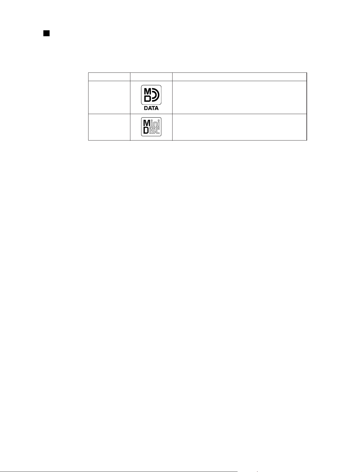
DISC FOR MD4S
MD4S
5
It's important that you buy the correct type of disc for use with your MD4S. For 4-track recording and playback, you must use MD DATA discs.
Regular MiniDiscs can only be used for 2-track recording and playback (2 TR mode).
MD DATA discs are used as a storage media for computers. The MD4S uses the MD DATA audio format to store data on them. Regular MiniDiscs
are also referred to as MD discs, although they are used only for music.
New MD DATA discs do not require formatting before use with the MD4S. Discs that have been used to store computer data, however, must first be
formatted.
Regular MiniDisc decks cannot play MD DATA discs.
Regular MiniDiscs recorded on the MD4S can be played on a regular MiniDisc deck.
MiniDisc recordings made on a regular MiniDisc deck can be edited on the MD4S. MiniDiscs containing songs that were digitally copied from a
commercial CD, however, cannot be edited due to the SCMS (Serial Copy Management System) protection system.
Songs that were recorded in 8-track mode on a recorder such as the MD8 cannot be played back on the MD4S.
MD DATA
MiniDisc
Type Logo
MD DATA discs are for computer data storage applications.
You can purchase them at computer stores. This is the type
of disc you should buy for 4-track recording and playback
with your MD4S. Note that there are two types available:
playback only and rewritable. Buy the rewritable type.
MiniDiscs are used only for music. Two types are available:
playback only and recordable. The MD4S can record up to
two tracks on the recordable type and play the playback
only type.
Description
SPECIFICATIONS
MD4S
6
Recorder
Mixer
General
Digital/Audio
Rec/Play
Locate
Cue & review
Disc Editing
Song Editing
Track Editing
Title Editing
Panel Controls
MIDI
Display
Sampling Frequency: 44.1 kHz Compression: ATRAC
Frequency Response: 20 Hz–20 kHz, +1 dB, –3 dB
THD+N: Less than 0.02 % (1 kHz)
S/N: 96 dB typ.
4-track independent simultaneous record/play (Recording time: 37 min)
Dubbing with 4-track playback
Auto & Manual Punch In/Out (11.6 ms accuracy)
Four-track (37 min), Stereo (74 min), or Mono (148 min) record/play
Repeat play A-B, Single song, All song
Vari-pitch (+/-10 %)
Start and End point of Song Direct Time Locate
10 Marker locate points for each song Last Recording In/Out point
0.5x, 2x, 4x, 8x, 16x, 32x play speed
Disc Erase
Copy, Move, Divide, Combine, Renumber, Erase
Track Copy, Part Copy, Track Erase, Part Erase
Disc title, Song title
REC SELECT buttons 1–4, BUS button
Transport buttons: PLAY, STOP, PAUSE, REC, REHE, SONG SEARCH, EJECT
Mode buttons: AUTO PUNCH I/O, EDIT, UTILITY, ADJUST, PITCH, PEAK HOLD, DISPLAY, EXIT
CURSOR shuttle/DATA dial
Locate buttons: MARK, MARK SEARCH, LAST REC (IN/OUT), SEARCH, SET, REPEAT, A B
MIDI IN, OUT, THRU jacks
FLD (Fluorescent Display)
Inputs
Outputs
Frequency response
EQ
MASTER Channel Features
MIC/LINE IN (CH1, 2) Balanced phone jack x2 (–10 to –50 dB)
MIC/LINE IN (CH1, 2) Balanced XLR x2 (–10 to –50 dB)
MIC/LINE INPUT (CH3–4) Unbalanced phone jack x2 (–10 to –50 dB)
LINE INPUT (CH5–8) Unbalanced phone jack x4 (–10 dB)
INSERT IN/OUT (CH 1, 2) TRS phone jack x2 (–10 dB)
2 TR IN (L, R) Phono x2 (–10 dB)
TRACK DIRECT OUT (1–4) Phono x4(–10 dB)
STEREO OUT (L, R) Phono x2 (–10 dB)
MONITOR OUT (L, R) Phono x2 (–10 dB)
AUX SEND (1, 2) Phone jack x2 (–10 dB)
PHONES OUT Stereo phone jack (8–40 ohm)
20 Hz–20 kHz +1, –3 dB
3-band, +/-15 dB (LOW: 100 Hz shelving, MID: Peaking (2.5 kHz), HIGH: 10 kHz Shelving)
Stereo Fader (45 mm), Monitor Level control, Monitor Select buttons (2 TR IN, STEREO, CUE), CUE MIX TO
STEREO buttons
Power Requirements
Power Consumption
Dimensions (W x H x D)
Weight
Operating Conditions
Supplied Accessories
Optional Accessories
Output Level
USA & Canada: 120 V/60 Hz, Others: 230 V/50 Hz
24 W
413 x 109.5 x 388 mm
5.2 kg
Temperature: 5 ˚C–35 ˚C (41 ˚F–95 ˚F), Humidity: 10 %–95 %
AC power cord, Owner’s Manual
FC5 Footswitch
Refer to the INSPECTION SPECIFICATION Section of this manual.
0 dB is referenced to 0.775 V r.m.s.
TOC WRITE
REHE REC PLAY STOP
PAUSE
IN OUT
SONG SEARCH
LAST REC SEARCH
MARK SEARCHREPEAT
AUTO
PUNCH I/O
AB
DATA CURSOR
PHONES PUNCH I/O
PITCH
EJECT
ADJUST EDIT UTILITY
CH1
BUS
CH2
REC SELECT
CH3 CH4
LRLR
PEAK HOLD DISPLAY
MULTITRACK MD RECORDER
1234
EXIT
ENTER
SET
MARK
1
1
GAIN
CUE
HIGH
LINE
FLIP
MIC/
LINE
MIC
LR
010
–15 +15
MID
–15 +15
LOW
–15 +15
PAN
LR
AUX
12
PB
10
9
8
7
6
5
4
3
2
1
0
P
A
N
L
E
V
E
L
2
2
GAIN
CUE
HIGH
LINE
FLIP
MIC/
LINE
MIC
LR
010
–15 +15
MID
–15 +15
LOW
–15 +15
PAN
LR
AUX
12
PB
10
9
8
7
6
5
4
3
2
1
0
P
A
N
L
E
V
E
L
3
3
GAIN
CUE
HIGH
LINE
FLIP
MIC/
LINE
MIC
LR
010
–15 +15
MID
–15 +15
LOW
–15 +15
PAN
LR
AUX
12
PB
10
9
8
7
6
5
4
3
2
1
0
P
A
N
L
E
V
E
L
4
4
GAIN
CUE
HIGH
LINE
FLIP
MIC/
LINE
MIC
LR
010
–15 +15
MID
–15 +15
LOW
–15 +15
PAN
LR
AUX
12
PB
10
9
8
7
6
5
4
3
2
1
0
P
A
N
L
E
V
E
L
5 / 6 7 / 8
010010
STEREO
MONITOR LEVEL
CUE
STEREO
2TR IN
CUE MIX TO STEREO
MONITOR SELECT
10
9
8
7
6
5
4
3
2
1
0
10
9
8
7
6
5
4
3
2
1
0
MIN MAX
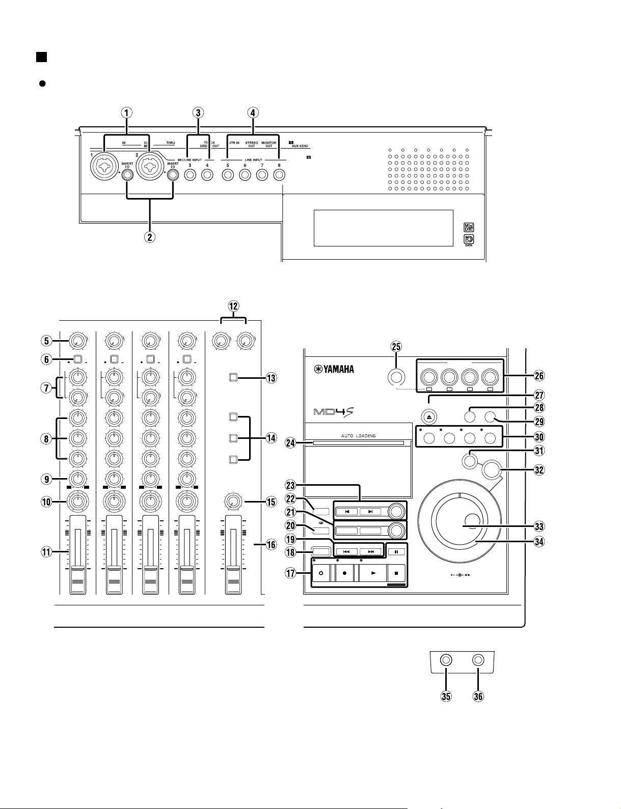
PANEL LAYOUT
MD4S
7
Control Panel

MD4S
8
POWER switch
AC IN
AUX SEND 1, 2 jacks
MONITOR OUT jacks
STEREO OUT jacks
2TR IN jacks
TRACK DIRECT OUT 1-4 jacks
MIDI IN, OUT, THRU connectors
Rear Panel
Rear Panel
MIC/ LINE INPUT 1, 2 terminals
INSERT I/O 1, 2 jacks
MIC/ LINE INPUT 3, 4 jacks
LINE INPUT 5-8 jacks
GAIN control
FLIP switch
CUE PAN/ CUE LEVEL controls
EQ (HIG, MID, LOW) controls
AUX control
PAN control
Fader
Level (5/ 6), (7/ 8) controls
CUE MIX TO STEREO switch
MONITOR SELECT (2TR IN, STEREO, CUE)
switches
MONITOR LEVEL control
STEREO fader
Disk transport (REHE, REC, PLAY, PAUSE,
STOP/ TOC WRITE) buttons
AUTO PUNCH I/O button
SONG SEARCH ( , ) buttons
A B repeat button
LAST REC SEARCH (IN, OUT), SET buttons
REPEAT button
MARK SEARCH ( , ), MARK buttons
Disc compartment
BUS button
REC SELECT buttons
EJECT button
PEAK HOLD button
DISPLAY button
Function (PITCH, ADJUST, EDIT, UTILITY)
buttons
EXIT button
ENTER button
DATA dial (DATA + -)
CURSOR shuttle
PHONES jack
PUNCH I/O jack
Control Panel
Top panel connectors
Mono Inputs
Stereo Inputs
Disc transport section
Front Panel
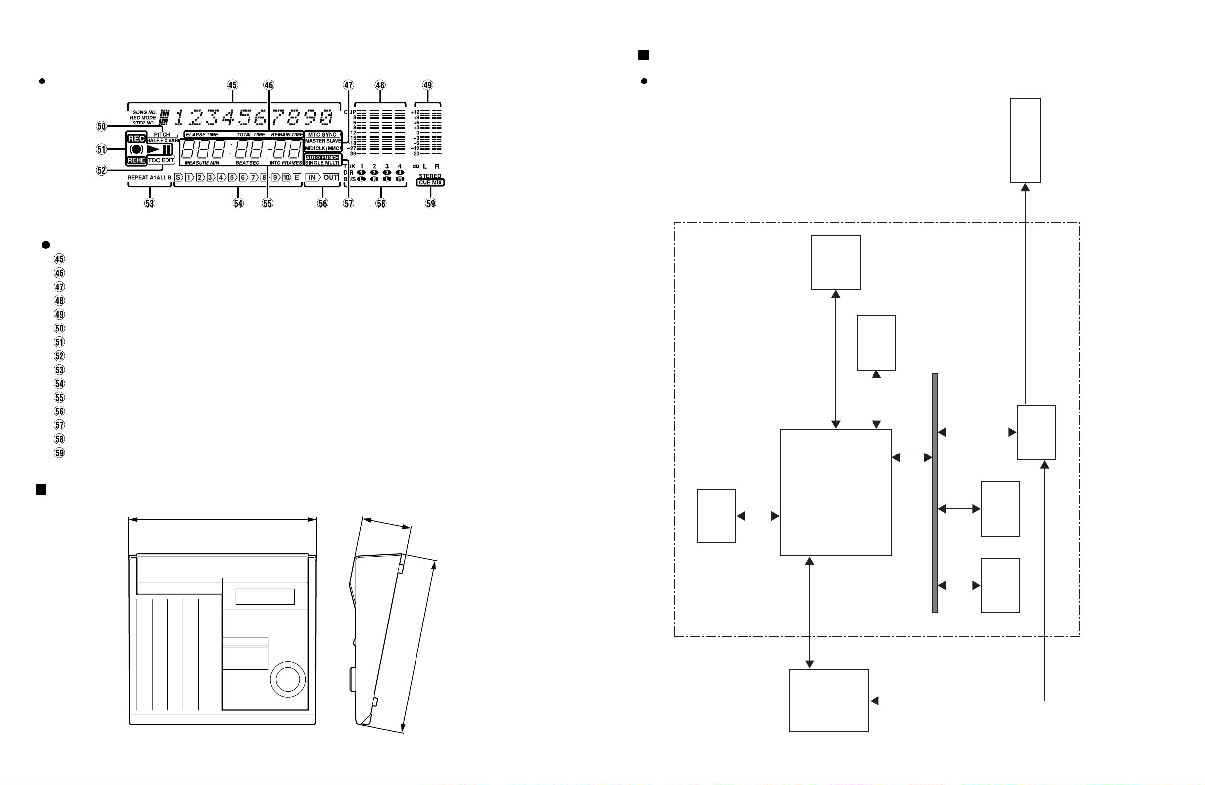
Title and function display
Time counter mode
MIDI indicators
Track level meters
Stereo level meter
Pitch indicator
Status indicators
TOC EDIT indicator
Repeat indicator
Marker indicators
Time counter
IN, OUT indicators
Auto punch indicator
Track recording indicators
CUE MIX indicator
Display
Display
MD4S
9
DIMENSIONS
W: 413
H: 109.5
D: 388
Unit : mm
BLOCK DIAGRAM
MEMORY
CONTROL
ATRAC
AUDIO
INTERFACE
IC 101
IC 203
ROM
IC 104
AD / DA
IC 301
IC 302
SRAM
IC 103
M-Com
IC 109
DRAM
IC 102
FL DISPLAY
SUB SHEET
MD
MECHA
UNIT
MAIN Part
TRACK 1
TRACK 2
TRACK 3
TRACK 4
RECORDER
STEREO METER
MIC/LINE
INSERT I/O
1,2
2TR IN
L
R
PAN
CUE PAN
FLIP
LOW HIGH
MID
GAIN
MONITOR
SELECT
AUX
2TR IN
STERO
CUE
STEREO
FADER
1
2
AUX SEND
R
L
R
L
STEREO
OUT
MONITOR
OUT
PHONES
1
2
3
4
TRACK
DIRECT
OUT
MONITOR
LEVEL
DIRECT
1,2
PB
1,2
CUE
1,2
M/L
PB
M/L
PB
STEREO CUEAUX
LR LR
CUE 1 ~ 4PB 1 ~ 4DIRECT 1 ~ 4
1
2
3
4
L
RRL
AD1
AD2
AD3
AD4
DA1
DA2
DA3
DA4
PB
RECPBRECPBRECPBREC
1
2
MIC/LINE
3,4
PAN
CUE PAN
FLIP
GAIN
AUX
FADER
DIRECT
3,4
PB
3,4
CUE
3,4
M/L
PB
M/L
PB
1,2
LINE 6,8
LINE 5,7
INPUT LEVEL
CUE MIX TO STEREO
CUE LEVEL
CUE LEVEL
IC101 IC103,104 IC107
IC109
VR101
VR201
VR102
VR202
VR103
VR203
VR104
VR204
LOW HIGH
MID
VR302
VR402
VR301
VR401
SW103
SW104
VR303
VR403
VR304
VR404
VR105
VR205
VR108
VR109,209
SW105
SW106
SW
107
SW108
VR106,206
VR107,207
VR309,409
VR306,406
VR307,407
VR208
VR305
VR405
VR308
VR408
VR501
VR502
1,7
6721 3,51,7
3,5 1,7
IC108IC105,106
3,5127
IC102
1,7
61,7
IC113 VR503
67
21
IC114
67
IC120
75
13
21
IC119
67
21
IC118 VR504
67
21
IC116
67
21
IC117
67
21
IC112
67
IC111
67
IC112
21
IC115
67
21
IC111
21
IC110
3,5 1,7
SW101
SW102
KEC-92344
MD4S
10
Mixer Part
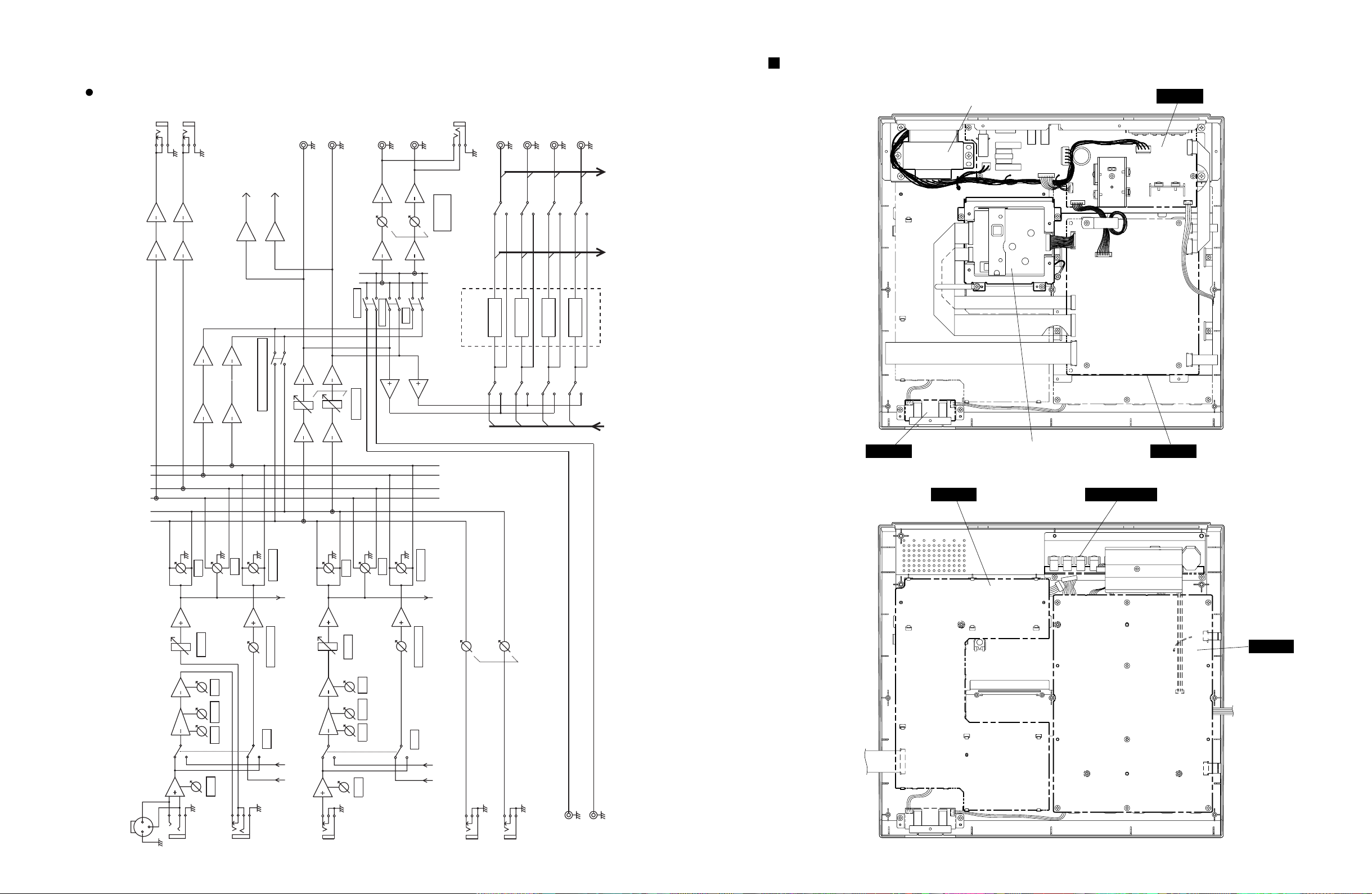
CIRCUIT BOARD LAYOUT
SUB 2/3
SUB 3/3
SUB 1/3
MIX 2/2 (INPUT)
MIX 1/2
MAIN
Power transformer
MD mechanical unit

MD4S
11
[
520A
]: Bind Head Tapping Screw-B 3.0 X 8 MFZN2BL (EP600190)
(Fig. 1)
Bottom cover
[
520A
][
520A
]
DISASSEMBLY PROCEDURE
1. Bottom Cover
1-1 Remove the twelve (12) screws marked [520A].
The bottom cover can then be removed. (Fig. 1)
2. MAIN Circuit Board
2-1 Remove the bottom cover. (See Procedure 1.)
2-2 Remove the screw marked [530] and the three
(3) screws marked [520B]. The MAIN circuit
board can then be removed. (Fig. 2)
3. MD Mechanical Unit
3-1 Remove the bottom cover. (See Procedure 1.)
3-2 Remove the four (4) screws marked [520C] and
the screw marked [520D]. The MD mechanical
unit can then be removed. (Fig. 2)
4. SUB 1/3 Circuit Board
4-1 Remove the SHUTTLE knob and JOG knob. (Fig.3)
4-2 Remove the bottom cover. (See Procedure 1.)
4-3 Remove the MD mechanical unit. (See Procedure 3.)
4-4 Remove the two (2) screws marked [520E] and
the four (4) screws marked [500]. The sub chassis
with the SUB 2/3 circuit board and power
transformer can then be removed. (Fig. 2, 3)
4-5 Remove the SUB 1/3 circuit board while pressing
the twelve (12) hooks marked [A]. (Fig. 5)
5. SUB 2/3 Circuit Board
5-1 Remove the bottom cover. (See Procedure 1.)
5-2 Remove the two (2) screws marked [520E], the
six (6) screws marked [520F] and the four (4)
screws marked [520G]. The SUB 2/3 circuit
board can then be removed. (Fig. 2, 3)
5-3 Remove the POWER button from the SUB 2/3
circuit board.
6. SUB 3/3 Circuit Board
6-1 Remove the bottom cover. (See Procedure 1.)
6-2 Remove the two (2) screws marked [520H]. The
SUB 3/3 circuit board can then be removed.
(Fig. 2)
6-3 Remove the two (2) U-shaped holders marked
[410A], then remove the support JACK from the
SUB 3/3 circuit board. (Fig. 6)
[
520
]: Bind Head Tapping Screw-B 3.0 X 8 MFZN2BL (EP600190)
[
490
]: Bind Head Screw 4.0 X 8 MFZN2BL (EG340360)
[
500
]: Bind Head Tapping Screw-P 4.0 X 12 MFZN2BL (VA847600)
[
520
]: Bind Head Tapping Screw-B 3.0 X 8 MFZN2BL (EP600190)
[
530
]: Screw 3B-8Y9294 (VR602100)
(Fig. 4)
(Fig. 3)
(Fig. 2)
POWER button
MAIN Holder
FADER knobs JOG knob SHUTTLE knob
MD mechanical unit
Power transformer
[
520E
]
[
520F
]
[
500
]
[
520B
]
[
520I
]
[
520D
]
[
520C
]
[
500
]
[
490
][
520G
]
[
520B
][
520H
]
[
520B
]:Japanese
Model
[
530
]
MAIN
SUB3/3
SUB2/3

MD4S
12
Top cover
Support JACK
SUB1/3
[A]
[
410A
]
(Fig. 5) (Fig. 6)
[
410A
]: U-shaped Holder MET41-0191 (VI549000)
7. MIX 1/2 Circuit Board
7-1 Remove the five (5) FADER knobs. (Fig. 3)
7-2 Remove the bottom cover. (See Procedure 1.)
7-3 Remove the SUB 2/3 circuit board. (See Procedure 5.)
7-4 Remove the MAIN circuit board. (See Procedure 2.)
7-5 Remove the four (4) screws marked [520I] and
the screw marked [520D]. The MAIN holder
can then be removed. (Fig. 2)
7-6 Remove the MD mechanical unit. (See Procedure 3.)
7-7 Remove the eight (8) screws marked [520J].
The MIX 1/2 circuit board can then be removed.
(Fig. 7)
8. MIX 2/2 (INPUT) Circuit Board
8-1 Remove the bottom cover. (See Procedure 1.)
8-2 Remove the two (2) screws marked [520E] and
the four (4) screws marked [500]. The power
transformer with the SUB 2/3 circuit board can
then be removed. (Fig. 2, 3)
8-3 Remove the screw marked [510]. The shield
INPUT can then be removed. (Fig. 7)
8-4 Remove the two (2) screws marked [520K]. The
MIX 2/2 (INPUT) circuit board can then be
removed. (Fig. 7)
8-5 Remove the four (4) screws marked [520L] and
the two (2) U-shaped holders marked [410B].
The support JACK can then be removed from
the MIX 2/2 (INPUT) circuit board. (Fig. 8)
9. Power Transformer
9-1 Remove the bottom cover. (See Procedure 1.)
9-2 Remove the two (2) screws marked [490]. The
power transformer can then be removed. (Fig. 2)
Shield INPUT
MIX2/2 (INPUT
)
MIX1/2
[
510
]
[
520K
]
[
520J
]
[
520L
][
410B
]
(Fig. 7)
(Fig. 8)
[
510
]: Bind Head Screw 3.0 X 6 MFZN2BL (EG330360)
[
520
]: Bind Head Tapping Screw-B 3.0 X 8 MFZN2BL (EP600190)
[
410B
]: U-shaped Holder MET41-0191
(VI549000)
[
520L
]: Bind Head Tapping Screw-B 3.0 X 8 MFZN2BL
(EP600190)

MD4S
13
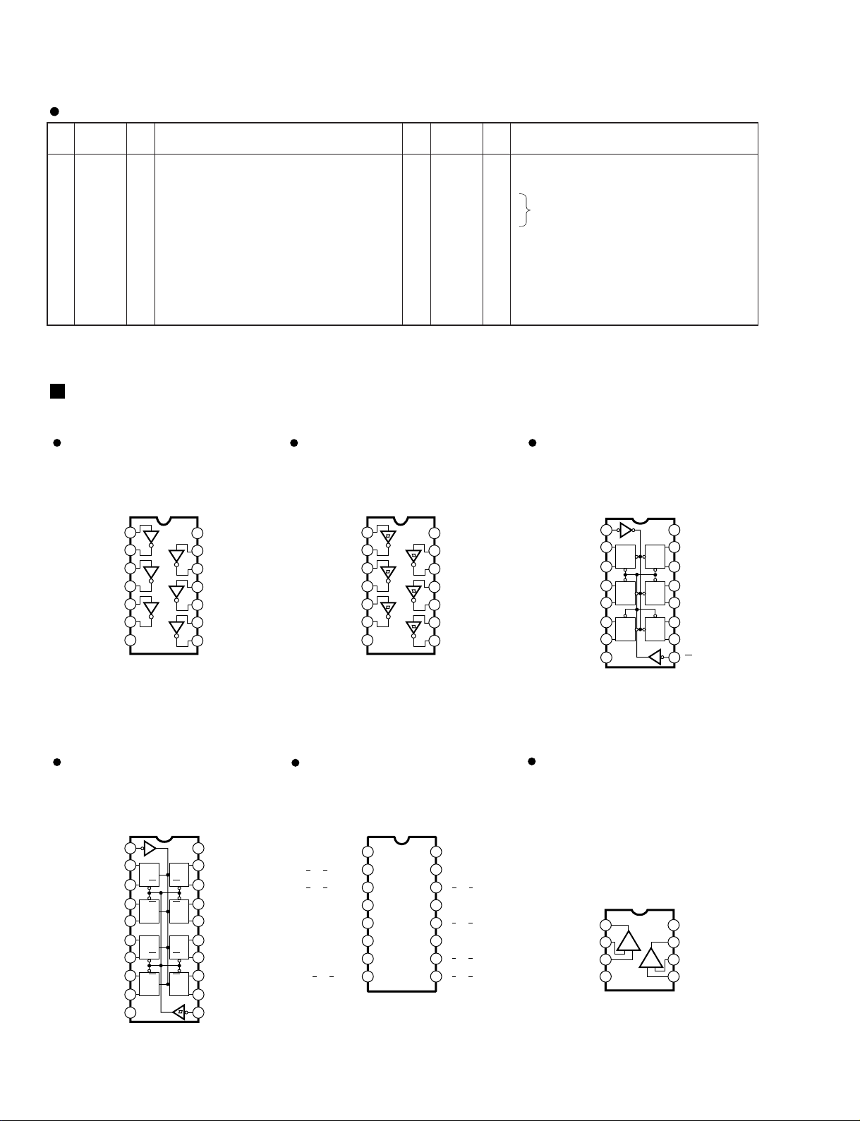
LSI PIN DESCRIPTION
PIN
NO.
1
2
3
4
5
6
7
8
9
10
11
12
13
14
15
16
17
18
19
20
21
22
23
24
25
26
27
28
29
30
31
32
33
34
35
36
37
38
39
40
41
42
43
44
45
46
47
48
49
50
I/O
I/O
I/O
I/O
I/O
I/O
I/O
I
I
O
O
O
I
I
I/O
I/O
I/O
I/O
I/O
I/O
I/O
I/O
I/O
I/O
I/O
I/O
I/O
I/O
I/O
I/O
I/O
I/O
O
O
O
O
O
O
O
O
O
O
O
O
O
O
VCC
PB0
PB1
PB2
PB3
PB4
PB5
PB6//DREQ0
PB7//DREQ1
/RES0
VSS
P90/TXD0
P91/TXD1
P92/RXD0
P93/RXD1
P94/SCK0
P95/SCK1
P40/D0
P41/D1
P42/D2
P43/D3
VSS
P44/D4
P45/D5
P46/D6
P47/D7
D8
D9
D10
D11
D12
D13
D14
D15
VCC
A0
A1
A2
A3
A4
A5
A6
A7
VSS
A8
A9
A10
A11
A12
A13
NAME
Power supply (+5 V)
Port B
Port B/DMA request
Reset output
Ground
Port 9/Transmission data
Port 9/Reception data
Port 9/Serial clock
Port 4/Data bus
(Ground)
Data bus
Power supply (+5 V)
Address bus
(Ground)
FUNCTION
PIN
NO.
51
52
53
54
55
56
57
58
59
60
61
62
63
64
65
66
67
68
69
70
71
72
73
74
75
76
77
78
79
80
81
82
83
84
85
86
87
88
89
90
91
92
93
94
95
96
97
98
99
100
I/O
O
O
O
O
O
O
I
I
O
O
I
I
I
I
I
O
O
O
O
I
I
I
I
I
I
I
I
I
I
I
I
O
O
O
O
I/O
I/O
I/O
I/O
I/O
I/O
I/O
I/O
A14
A15
A16
A17
A18
A19
VSS
P60//WAIT
P61//BREQ
P62//BACK
Ø
/STBY
/RES
NMI
VSS
EXTAL
XTAL
VCC
/AS
/RD
/HWR
/LWR
MD0
MD1
MD2
AVCC
VREF
P70/AN0
P71/AN1
P72/AN2
P73/AN3
P74/AN4
P75/AN5
P76/AN6
P77/AN7
AVSS
P80//RFRSH
P81//CS3
P82//CS2
P83//CS1
P84//CS0
VSS
PA0
PA1
PA2
PA3
PA4
PA5
PA6
PA7
NAME
Address bus
Ground
Port 6 /Wait
Port 6/Bus request
Port 6/Bus acknowledge
System clock
Stand-by mode signal
Reset
Non-maskable interrupt
Ground
Crystal oscillator
Crystal oscillator
Power supply (+5 V)
Address strobe
Read strobe
High write
Low write
Mode select (mode 1 – 4)
Power supply for ADC
Reference voltage for ADC
Port 7/Analog input
Ground for ADC
Port 8/Refresh
Port 8/Chip select
Ground
Port A
FUNCTION
HD6413002F16 (XP691A00) CPU MAIN IC109
PIN
NO.
1
2
3
4
5
6
7
8
9
10
11
12
13
14
15
16
17
18
19
20
21
22
23
24
25
26
27
28
29
30
31
32
33
34
35
36
37
38
39
40
41
42
43
44
45
46
47
48
49
50
51
52
53
54
55
56
57
58
59
60
I/O
I
I
I
O
O
I
I
I
I
O
O
I
I
O
I
O
I
I
I
O
O
I
I
I
O
O
I
I
I
I
I
I
I
I
I
I
I
I
I
I
I
I
I
I
I
I
I
I
I
I
I
I
I
I
I
I
VDD1
ACDI0
XABS0
C2PO0
XARQ0
ACDO0
SYNC0
ACDI1
XABS1
C2PO1
XARQ1
ACDO1
SYNC1
F86IA
F86OA
F86IB
F86OB
ACDI2
XABS2
C2PO2
XARQ2
ACDO2
SYNC2
ACDI3
XABS3
C2PO3
XARQ3
ACDO3
SYNC3
VSS1
TEST0
TEST1
TEST2
EXEC0
EXEC1
EXEC2
EXEC3
ATT0
ATT1
ATT2
ATT3
MUTE0
MUTE1
MUTE2
MUTE3
REC0
REC1
REC2
REC3
XLAT0
XLAT1
XLAT2
XLAT3
XRSTA
XRSTB
SCLK
SWDT
TA0
TA1
VSS2
NAME
Power supply
ATRAC data input 0
ATRAC data serial transfer synchronization pulse input 0
ATRAC data error flag 0
ATRAC data transfer demand 0
ATRAC data output 0
Signal input 0 for ATRAC data synchronized
ATRAC data input 1
ATRAC data serial transfer synchronization pulse input 1
ATRAC data error flag 1
ATRAC data forward demand 1
ATRAC data output 1
Signal input 1 for ATRAC data synchronized
Frame synchronized signal input A
Frame synchronized signal output A
Frame synchronized signal input B
Frame synchronized signal output B
ATRAC data input 2
ATRAC data serial transfer synchronization pulse input 2
ATRAC data error flag 2
ATRAC data f transfer demand 2
ATRAC data output 2
Signal input 2 for ATRAC data synchronized
ATRAC data input 3
ATRAC data serial forward synchronization pulse input 3
ATRAC data error flag 3
ATRAC data transfer demand 3
ATRAC data output 3
Signal input 3 for ATRAC data synchronized
Ground
Test terminal
Test terminal
Test terminal
Start / Stop establishment input 0 (“H”=START)
Start / Stop establishment input 1 (“H”=START)
Start / Stop establishment input 2 (“H”=START)
Start / Stop establishment input 3 (“H”=START)
Attenuation establishment input 0 (“H”=-12dB)
Attenuation establishment input 1 (“H”=-12dB)
Attenuation establishment input 2 (“H”=-12dB)
Attenuation establishment input 3 (“H”=-12dB)
Mute establishment input 0 (“H”=mute on)
Mute establishment input 1 (“H”=mute on)
Mute establishment input 2 (“H”=mute on)
Mute establishment input 3 (“H”=mute on)
REC/PLAY establishment input 0 (“H”=REC)
REC/PLAY establishment input 1 (“H”=REC)
REC/PLAY establishment input 2 (“H”=REC)
REC/PLAY establishment input 3 (“H”=REC)
Latch pulse input 0 of serial interface
Latch pulse input 1 of serial interface
Latch pulse input 2 of serial interface
Latch pulse input 3 of serial interface
Reset input A
Reset input B
Transfer clock input of serial interface
Data input of serial interface
Test terminal (Connect it with the ground.)
Test terminal (Connect it with the ground.)
Ground
FUNCTION
CXD2538R (XU964A00) ATRAC MAIN IC203
PIN
NO.
61
62
63
64
65
66
67
68
69
70
71
72
73
74
75
76
77
78
79
80
81
82
83
84
85
86
87
88
89
90
91
92
93
94
95
96
97
98
99
100
101
102
103
104
105
106
107
108
109
110
111
112
113
114
115
116
117
118
119
120
I/O
I
I
I
I
I
I
I
I
O
I
O
I
O
I
I
I
I
I
I
I
I
I
I
I
I
I
I
I
I
O
O
I
I
I
I
I
I
I
I
I
I
I
I
I
I
I
I
I
I
I
I
I
I
I
I
I
I
VDD2
XILT
IDSL
SICK
DIDT
ACLK
BCK
LRCK
ADIN0
DOUT0
ADIN1
DOUT1
ADIN2
DOUT2
ADIN3
DOUT3
TA2
TA3
TA4
TA5
TA6
TA7
TA8
TA9
TA10
TA11
TA12
TD0
TD1
VSS
OSCI
OSCO
SP0
TD2
TD3
TD4
TD5
TD6
TD7
TD8
TD9
TD10
TD11
TD12
TA13
TA14
TA15
TA16
TA17
TA18
TA19
TA20
TA21
TA22
TA23
TS0
TS1
TS2
TS3
VSS4
NAME
Power supply
Test terminal (Connect it with the power supply.)
Test terminal (Connect it with the power supply.)
Test terminal (Connect it with the power supply.)
Test terminal (Connect it with the power supply.)
Serial transfer clock (128 Fs) input of ATRAC data
2.8224 MHz (64 Fs)
44.1 kHz (Fs)
REC audio data input 0
Replay audio data output 0
REC audio data input 1
Replay audio data output 1
REC audio data input 2
Replay audio data output 2
REC audio data input 3
Replay audio data output 3
Test terminal (Connect it with the ground.)
Ground
Crystal oscillator input (1024 Fs)
Crystal oscillator output (1024 Fs)
1/2 oscillator output (512 Fs)
Test terminal (Connect it with the ground.)
Ground
FUNCTION

MD4S
14
PIN
NO.
1
2
3
4
5
6
7
8
9
10
11
12
13
14
15
16
17
18
19
20
21
22
23
24
25
26
27
28
29
30
31
32
33
34
35
36
37
38
39
40
41
42
43
44
45
46
47
48
49
50
51
52
53
54
55
56
57
58
59
60
61
62
63
64
65
66
67
68
69
70
71
72
73
74
75
76
77
78
79
80
81
82
83
84
85
86
87
88
89
90
91
92
93
94
95
96
97
98
99
100
101
102
103
104
I/O
O
I/O
I
I
O
I
O
O
O
O
O
O
O
O
O
O
O
O
I
I
I
O
O
O
O
O
O
O
I+/O
I+/O
I+/O
I+/O
I+/O
I+/O
I+/O
I+/O
I+/O
I+/O
I+/O
I+/O
I+/O
I+/O
I+/O
I+/O
O
O
I
I
I
I
O
I
I
I
O
I+/O
I+/O
I+/O
I+/O
I+/O
I+/O
I+/O
I+/O
I+/O
I+/O
I+/O
I+/O
I
O
I+/O
I+/O
I+/O
I+/O
I
I
I
I
I
I
I
I
I
I
I
I
I
I
I
I
I
VSS
LWRT
DDATA
DC2PO
ADSY
REC
(VSS)
MTYP
A0
A1
A2
VDD
A3
A4
A5
A6
A7
A8
A9
A10
A11
VSS
VDD
DBCK
DLRCK
MCKI
MCKO
DMCKO
XRAS
XUCAS
XLCAS
XWE
XOE
(VSS)
D0
D1
D2
D3
D4
D5
VSS
D6
D7
D8
D9
D10
D11
D12
D13
D14
D15
VDD
GND
XCSRA
SFCLK
XSAS
XSWRH
XSWRL
XSRD
XINT
XLAT
XRST
XTCL
VCC
XBUSY
SD15
SD14
SD13
SD12
SD11
SD10
SD9
SD8
SD7
SD6
SD5
SD4
GND
VCC
MIDCKI
MIDCKO
SD3
SD2
SD1
SD0
SA13
SA12
SA11
SA10
SA9
SA8
SA7
GND
SA6
SA5
SA4
SA3
SA2
SA1
SA0
SA16
SA17
SA18
VCC
NAME
Ground
Laser power control
REC/PLAY data
C2 Error flag input
ADIP sync input
REC/PLAY select signal
Ground
DRAM type select
DRAM Address A0
DRAM Address A1
DRAM Address A2
Power supply
DRAM Address A3
DRAM Address A4
DRAM Address A5
DRAM Address A6
DRAM Address A7
DRAM Address A8
DRAM Address A9
DRAM Address A10
DRAM Address A11
Ground
Power supply
DDATA I/O Bit clock
LRCK for DIF
Clock input for DIF
Clock output for DIF
Master clock output
DRAM RAS signal
DRAM CAS signal (HIGH_BYTE)
DRAM CAS signal (LOW BYTE)
DRAM write signal
DRAM read signal
Ground
DRAM data Bit 0
DRAM data Bit 1
DRAM data Bit 2
DRAM data Bit 3
DRAM data Bit 4
DRAM data Bit 5
Ground
DRAM data Bit 6
DRAM data Bit 7
DRAM data Bit 8
DRAM data Bit 9
DRAM data Bit 10
DRAM data Bit 11
DRAM data Bit 12
DRAM data Bit 13
DRAM data Bit 14
DRAM data Bit 15
Power supply
Ground
Chip select signal (for SRAM)
Sound frame synchronized clock
CPU address strove signal
CPU write signal (HIGH BYTE)
CPU write signal (LOW BYTE)
CPU read signal
Interrupt flag output
ATRAC command data latch pulse signal signal
Reset signal
Reset signal for test
Power supply
CPU wait signal output
CPU data Bit 15
CPU data Bit 14
CPU data Bit 13
CPU data Bit 12
CPU data Bit 11
CPU data Bit 10
CPU data Bit 9
CPU data Bit 8
CPU data Bit 7
CPU data Bit 6
CPU data Bit 5
CPU data Bit 4
Ground
Power supply
Clock input for MIDI
Clock output for MIDI
CPU data Bit 3
CPU data Bit 2
CPU data Bit 1
CPU data Bit 0
CPU address A13
CPU address A12
CPU address A11
CPU address A10
CPU address A9
CPU address A8
CPU address A7
Ground
CPU address A6
CPU address A5
CPU address A4
CPU address A3
CPU address A2
CPU address A1
CPU address A0
CPU address A16
CPU address A17
CPU address A18
Power supply
FUNCTION
PIN
NO.
105
106
107
108
109
110
111
112
113
114
115
116
117
118
119
120
121
122
123
124
125
126
127
128
129
130
131
132
133
134
135
136
137
138
139
140
141
142
143
144
145
146
147
148
149
150
151
152
153
154
155
156
157
158
159
160
161
162
163
164
165
166
167
168
169
170
171
172
173
174
175
176
177
178
179
180
181
182
183
184
185
186
187
188
189
190
191
192
193
194
195
196
197
198
199
200
201
202
203
204
205
206
207
208
I/O
I
I/O
I/O
I/O
I/O
I/O
I/O
I/O
I/O
O
O
O
I
I/O
I/O
I/O
I/O
I/O
I/O
I/O
I/O
O
O
O
O
O
I
I
O
O
O
O
I
I
O
O
I
I
O
O
O
I
I
O
O
O
O
O
O
O
I
O
I
O
I
I
I
I
I
O
O
O
O
O
I
O
I
O
O
O
O
O
O
I/O
I/O
VSS
SA19
EXTIOAO
EXTIOA1
EXTIOA2
EXTIOA3
(VDD)
EXTIOA4
EXTIOA5
EXTIOA6
EXTIOA7
VSS
XCS1
XCS2
XCS3
MTCIN
EXTIOB0
EXTIOB1
EXTIOB2
EXTIOB3
(VSS)
EXTIOB4
EXTIOB5
EXTIOB6
EXTIOB7
VDD
VSS
ACLK
XLATPB
XABSPB
ADTOB
AC2B
XARQPB
DECB
XLATPA
XABSPA
ADTOA
AC2A
XARQPA
DECA
VDD
XLATRB
XABSRB
ADTIB
XARQRB
ENCB
XLATRA
XABSRA
ADTIA
XARQRA
ENCA
VDD
GND
A1024FS
A256FS
XABCK
ABCK
ALRCK
(GND)
DAB
ADB
DAA
ADA
VCC
MTCOUT
TOSEL 4
TOSEL 3
TOSEL 2
TOSEL 1
TOSEL 0
TEST 7
TEST 6
TEST 5
TEST 4
TEST 3
VRCKI
VRCKO
GND
VCC
VCOI
VCOO
TEST 2
TEST 1
TEST 0
PDOUTN
PDOUTP
EXTIOCO
EXTIOC1
EXTIOC2
EXTIOC3
EXTIOC4
EXTIOC5
GND
EXTIOC6
EXTIOC7
EXTIOD0
EXTIOD1
EXTIOD2
EXTIOD3
EXTIOD4
EXTIOD5
EXTIOD6
EXTIOD7
VCC
NAME
Ground
CPU address A19
Extension port A of bit 0
Extension port A of bit 1
Extension port A of bit 2
Extension port A of bit 3
Power supply
Extension port A of bit 4
Extension port A of bit 5
Extension port A of bit 6
Extension port A of bit 7
Ground
Spare 1 of chip select
Spare 2 of chip select
Spare 3 of chip select
MIDI time code input
Extension port B of bit 0
Extension port B of bit 1
Extension port B of bit 2
Extension port B of bit 3
Ground
Extension port B of bit 4
Extension port B of bit 5
Extension port B of bit 6
Extension port B of bit 7
Power supply
Ground
Clock for ATRAC data transfer transmission
Command data latch pulse for ATRAC (PB)
Busy flag for ATRAC (PB)
ATRAC decode data output (PB)
C2 error flag for ATRAC (PB)
Data demand signal from ATRAC (PB)
ATRAC decode data input (PB)
Command data latch pulse for ATRAC (PA)
Busy flag for ATRAC (PA)
ATRAC decode data output (PA)
C2 error flag for ATRAC (PA)
Data demand signal from ATRAC (PA)
ATRAC decode data input (PA)
Power supply
Command data latch pulse for ATRAC (RB)
Busy flag for ATRAC (RB)
ATRAC encode data input (RB)
Data demand signal from ATRAC (RB)
Signal output for ATRAC encode(RB)
Command data latch pulse for ATRAC (RA)
Busy flag for ATRAC (RA)
ATRAC encode data input (RA)
Data demand signal from ATRAC (RA)
Signal output for ATRAC encode(RA)
Power supply
Ground
Quartz Crystal output (1024Fs)
Quartz Crystal output (256Fs)
Quartz Crystal output (64Fs)
Quartz Crystal output (64Fs reverse)
Sampling frequency output for audio
Ground
DA signal output (CH3,4)
AD signal input (CH3,4)
DA signal output (CH1,2)
AD signal input (CH1,2)
Power supply
MIDI time code output (reverse)
Test mode select input 4
Test mode select input 3
Test mode select input 2
Test mode select input 1
Test mode select input 0
Test signal output 7
Test signal output 6
Test signal output 5
Test signal output 4
Test signal output 3
Counter clock input
Counter clock output
Ground
Power supply
Clock input for PLL
Clock output for PLL
Test signal output 2
Test signal output 1
Test signal output 0
Phase comparison output
Phase comparison output
Expansion port C of bit 0
Expansion port C of bit 1
Expansion port C of bit 2
Expansion port C of bit 3
Expansion port C of bit 4
Expansion port C of bit 5
Ground
Expansion port C of bit 6
Expansion port C of bit 7
Expansion port D of bit 0
Expansion port D of bit 1
Expansion port D of bit 2
Expansion port D of bit 3
Expansion port D of bit 4
Expansion port D of bit 5
Expansion port D of bit 6
Expansion port D of bit 7
Power supply
FUNCTION
MD4MC2 (XU849A00) GATE ARRAY MAIN IC101
MD4S
15
PIN
NO.
1
2
3
4
5
6
7
8
9
10
11
12
13
14
I/O
I
I
I
I
I
I
-
I
I
I
I
I
O
VREFH
VREFL
AINR+
AINR-
AINL+
AINL-
VA
AGND
DIF0
DIF1
LRCK
SCLK
SDTI
SDTO
NAME
Positive Voltage Reference Input, VA
Negative Voltage Reference Input, AGND
Rch Analog Positive Input
Rch analog Negative Input
Lch Analog Positive Input
Lch analog Negative Input
Analog Power Supply
Analog Ground
Audio Data Interface Format
Audio Data Interface Format
Input/Output Channel Clock
Audio Serial Data Clock
Audio Serial Data Input
Audio Serial Data Output
FUNCTION
PIN
NO.
15
16
17
18
19
20
21
22
23
24
25
26
27
28
I/O
I
I
I
I/O
I/O
I
-
-
I
I
I
O
O
O
MCLK
DEM0
DEM1
TST3
TST2
TST1
VD
DGND
/PWDA
/PWAD
CMODE
AOUTL
AOUTR
VCOM
NAME
Master Clock Input
De-emphasis Frequency Select
De-emphasis Frequency Select
Test Pins (Pull Down Pins)
Digital Power Supply
Digital Ground
DAC power-Down Mode
ADC power-Down Mode
Master Clock Select (“H”:384 fs,“L”:256 fs)
Lch Analog Output
Rch Analog Output
Common Voltage Output, VA/2
FUNCTION
AK4520A-VF-E2 (XT802A00) DAC & ADC MAIN IC301
IC BLOCK DIAGRAM
TC74HCU04AF-TP1 (XD660A00)
Hex Inverter
1
2
3
4
5
6
7
1A
1Y
2A
2Y
3A
3Y
Vss
14
13
12
11
10
9
8
VDD
6A
6Y
5A
5Y
4A
4Y
TC74HC14AF-TP1 (XD657A00)
Hex Inverter
1
2
3
4
5
6
7
1A
1Y
2A
2Y
3A
3Y
GND
14
13
12
11
10
9
8
VDD
6A
6Y
5A
5Y
4A
4Y
SN74HC174NSR (XD836A00)
Hex D-Type Flip-Flop
Q
Q
DC K C K
C K
DC K
GG
CLEAR
1Q
1D
2D
2Q
3D
3Q
GND
1 16
2 15
3 14
4 13
5 12
6 11
7 10
8 9
Vcc
6Q
6D
5D
5Q
4D
4Q
CK
Q
D
GG
Q
DC K
G
C K
Q
D
G
Q
D
SN74HC374ANSR (XQ042A00)
Octal 3-State D-Type Flip-Flop
Q
DCK
OE
Q
DCK
OE
Q
DCK
OE
Q
DCK
OE
OUTPUT
CONTROL
1Q
1D
2D
2Q
3Q
3D
4D
4Q
GND
1 20
2 19
3 18
4 17
5 16
6 15
7 14
8 13
9 12
10 11
Vcc
8Q
8D
7D
7Q
6Q
6D
5D
5Q
CLOCK
Q
DCK
OE
Q
DCK
OE
Q
DCK
OE
Q
DCK
OE
TC4053BF (XB738A00)
TC74HC4053AF (XR150A00)
Multiplexer/Demultiplexer
1
Switches IN/OUT
2
3
4
5
6
7
8
do. Y0
do. Z1
Z
Z0
Commons OUT/IN
Swiches IN/OUT
Control Inhibit
-DC Voltage Supply
do
V
DD
Y
X
X1
X0
A
B
C
9
10
11
12
13
14
15
16
+DC Voltage Supply
Commons OUT/IN Y
do. X
Swiches IN/OUT X0
do X0
Control Input A
do. B
do. C
Y1
Y0
Z1
Z
Z0
INH
VEE
V
SS
Y1
NJM4558MT-1 (IG103520)
NJM2068MD-T1 (XJ553A00)
NJM4556AMT1 (XQ138A00)
µPC4570G2 (XF291A00)
Dual Operational Amplifier
1
2
3
4-V
8
7
6
5
Output A +V
Non-Inverting
Input A
-DC Voltage Supply
+DC Voltage
Supply
Output B
Inverting
Input B
Non-Inverting
Input B
Inverting
Input A
+-
+-
MAIN IC106
MAIN IC105 MAIN IC307 – 309
MAIN IC111 MAIN IC113
IC108
MIX IC103 – 112
IC115, 120, 101, 102, 113, 114,
116 – 118, 119
MAIN IC303 – 306, 310, 311