

Yamaha LMY4-DA Service Manual
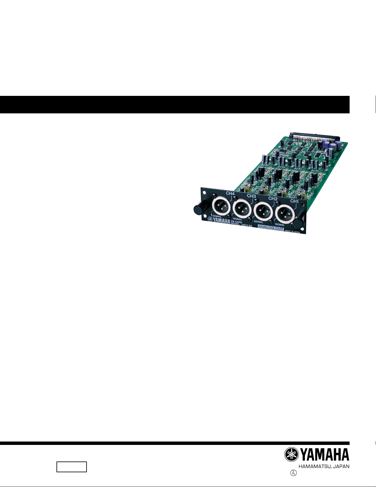
DA CARD
LMY4-DA
SERVICE MANUAL
PA
■ CONTENT
NOTICE OF CHANGES IN LMY4-DA S/M ............................... 3
SPECIFICATIONS .................................................................... 4
PANEL LAYOUT........................................................................ 4
DIMENSIONS ........................................................................... 4
BLOCK DIAGRAM .................................................................... 5
LSI PIN DESCRIPTION ............................................................ 6
IC BLOCK DIAGRAM................................................................ 7
CIRCUIT BOARD...................................................................... 8
TEST PROGRAM ................................................................... 10
PARTS LIST
OVERALL CIRCUIT BOARD
011504
*.**K-** K Printed in Japan '00.9

LMY4-DA
IMPORTANT NOTICE
This manual has been provided for the use of authorized Yamaha Retailers and their service personnel. It has been assumed that
basic service procedures inherent to the industry, and more specifically Yamaha Products, are already known and understood by the
users, and have therefore not been restated.
WARNING: Failure to follow appropriate service and safety procedures when servicing this product may result in personal injury,
destruction of expensive components, and failure of the product to perform as specified. For these reasons, we
advise all Yamaha product owners that all service required should be performed by an authorized Yamaha Retailer
or the appointed service representative.
IMPORTANT: The presentation or sale of this manual to any individual or firm does not constitute authorization, certification or
recognition of any applicable technical capabilities, or establish a principle-agent relationship of any form.
The data provided is believed to be accurate and applicable to the unit(s) indicated on the cover. The research, engineering, and
service departments of Yamaha are continually striving to improve Yamaha products. Modifications are, therefore, inevitable and
changes in specification are subject to change without notice or obligation to retrofit. Should any discrepancy appear to exist, please
contact the distributor's Service Division.
WARNING: Static discharges can destroy expensive components. Discharge any static electricity your body may have
accumulated by grounding yourself to the ground bus in the unit (heavy gauge black wires connect to this bus).
IMPORTANT: Turn the unit OFF during disassembly and part replacement. Recheck all work before you apply power to the unit.
WARNING: CHEMICAL CONTENT NOTICE!
The solder used in the production of this product contains LEAD. In addition, other electrical/electronic and /or plastic (where applicable)
components may also contain traces of chemicals found by the California Health and Welfare Agency (and possibly other entities) to
cause cancer and/or birth defects or other reproductive harm.
DO NOT PLACE SOLDER, ELECTRICAL/ELECTRONIC OR PLASTIC COMPONENTS IN YOUR MOUTH FOR ANY REASON WHATSOEVER!
Avoid prolonged, unprotected contact between solder and your skin! When soldering, do not inhale solder fumes or expose eyes to
solder/flux vapor!
If you come in contact with solder or components located inside the enclosure of this product, wash your hands before handling food.
2

■ NOTICE OF CHANGES IN LMY4-DA S/M
IC BLOCK DIAGRAM
Losic IC HD74LV245AFPEL (IS024500) is changed to Losic IC 74VHC245SJX (XY874A00)
TEST PROGRAM
Test program is newly provided. (Page 10)
LMY4-DA
3
LMY4-DA
■ SPECIFICATIONS
Output
Terminals
GAIN
switch
Actual Source
Impedance
+24 dB
CH 1-4
+18 dB
+15 dB
* 0 dB is referenced to 0.775 Vrns.
** 1=GND, 2=HOT, 3=COLD
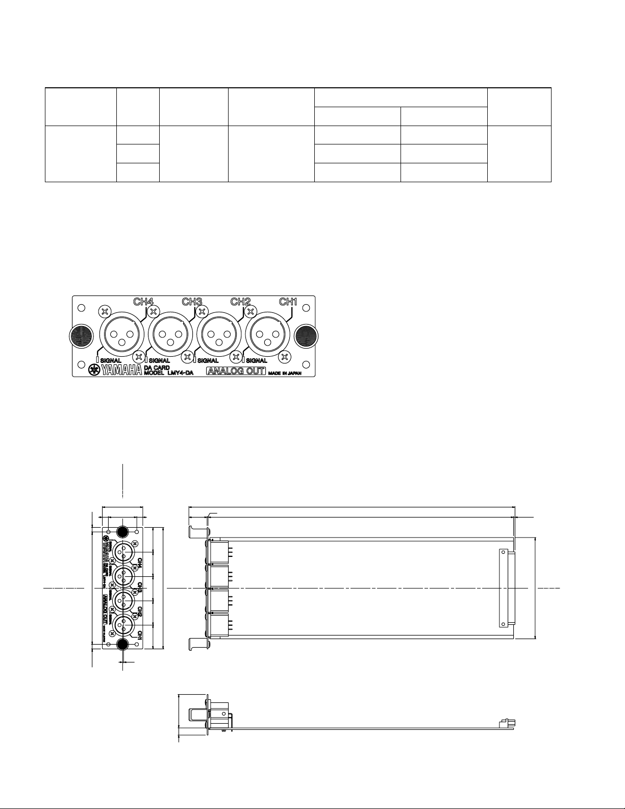
■ PANEL LAYOUT
150ohm
For Use With
Nominal
600ohm Lines
Output Level
Nominal
+10 dB (2.45 V)*
+4 dB (1.23 V)*
+1 dB (870 mV)*
Maximum. Before Clip
+24 dB (12.3 V)*
+18 dB (6.16 V)*
+15 dB (4.36 V)*
Connector
XLR-3-32 type
(Balanced)**
■ DIMENSIONS
40
66
28
4.5111
(4.5)
1
24.524
24
24
(23.5)
120
1
18
337
322.1
301.8
(1.3)
100
Unit: mm
4
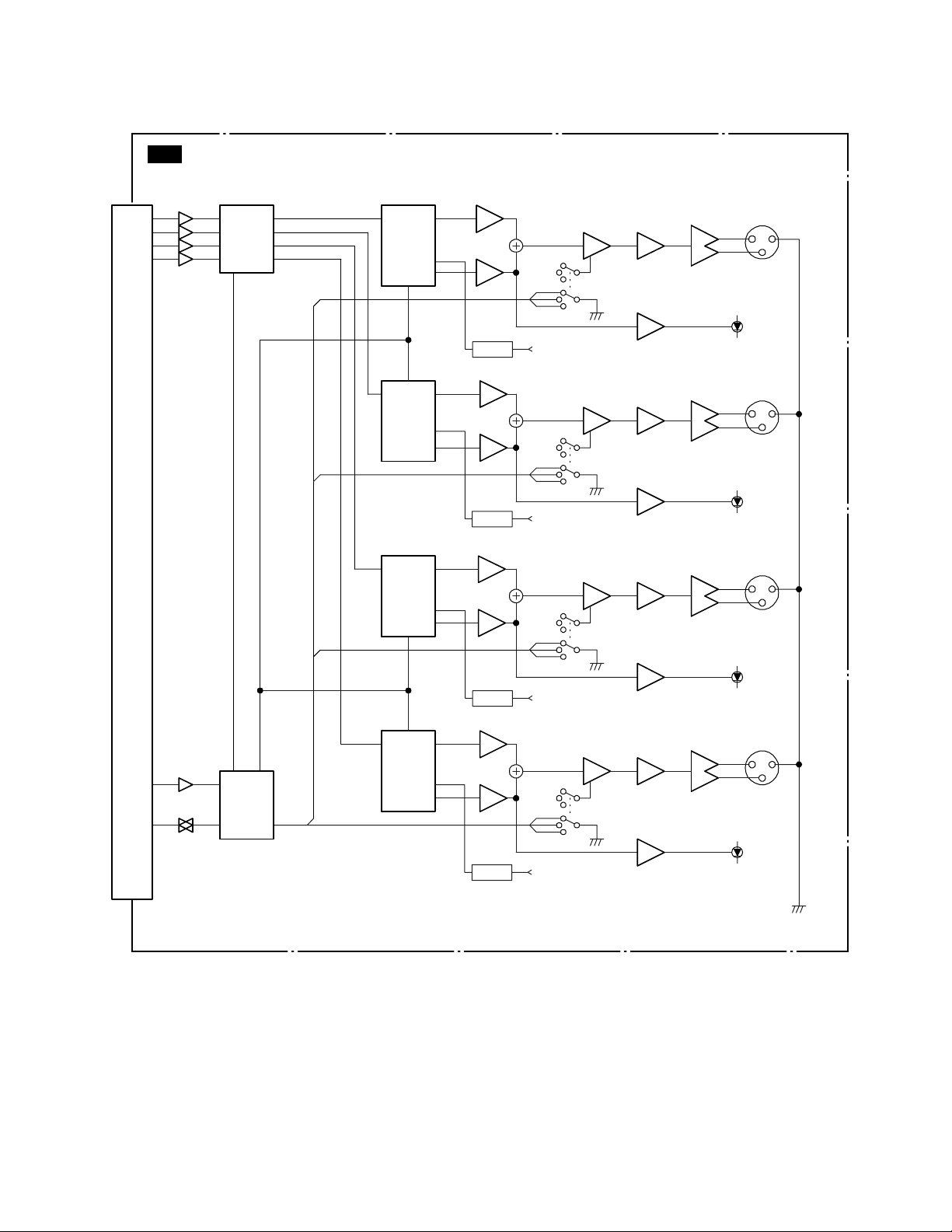
■ BLOCK DIAGRAM
DA
LMY4-DA
O1 a/3
O2 b/3
SYNCM
b/15
128FSM
b/17
A9 a/32
A8 b/31
A10 b/32
D00 a/34
D01 b/34
D02 a/35
D03 b/35
D04 a/36
D05 b/36
D06 a/37
D07 b/37
IC001, IC002
6
11
5
14
7
17
8
19
2-4
16-18
2-9
11-18
3
4
DAFC
5
IC007
6
33
/RES
/RESDA
16
15
Reg.
IC103, 104, 105
2
D/A
IC100
D/A
IC200
22-23
16-17
20-21
4
1-2
4
22-23
16-17
20-21
1-2
22-23
11
14
17
19
6
6
6
D/A
IC300
16-17
20-21
4
1-2
4
6
D/A
IC400
22-23
16-17
20-21
1-2
1
Amp
3
IC101
6
7
Amp
5
IC104
REGULATOR
2
1
Amp
3
IC201
6
7
Amp
5
IC204
REGULATOR
2
1
Amp
3
IC301
6
6
7
Amp
5
IC304
REGULATOR
2
1
Amp
3
IC401
6
7
Amp
5
IC404
REGULATOR
IC102 IC103
6
5
24dB
18dB
15dB
SW100
3
6
5
24dB
18dB
15dB
SW200
3
6
5
24dB
18dB
15dB
SW300
3
6
5
24dB
18dB
15dB
SW400
3
2
7
Amp
3
IC500
2
3
IC202 IC203
2
7
Amp
3
2
3
IC302
2
7
Amp
3
2
3
IC402
2
7
Amp
3
IC800
2
3
Amp
Amp
Amp
IC600
Amp
Amp
IC700
Amp
Amp
Amp
1
1
1
1
1
1
1
1
6
5
2
3
6
5
2
3
6
5
2
3
IC403
6
5
2
3
Amp
Amp
Amp
Amp
IC303
Amp
Amp
Amp
Amp
2
7
1
[SIGNAL]
2
7
1
[SIGNAL]
2
7
1
[SIGNAL]
2
7
1
[SIGNAL]
1
[CH1]
3
1
[CH2]
3
1
[CH3]
3
1
[CH4]
3
KEC-92518
5
LMY4-DA
■ LSI PIN DESCRIPTION
AK4393-VF-E2 (XW029A00) D/A CONVERTER
PIN
NAME I/O FUNCTION
No.
1
10
11
12
13
14
2
3
4
5
6
7
8
9
DVSS
DVDD
MCLK
PD
BICK
SDATA
LRCK
SMUTE
CS
DFS
DEM0
CCLK
DEM1
CDTI
DIF0
DIF1
DIF2
-
Digital Ground Pin
-
Digital Power Supply Pin, 3.3V or 5.0V
I
Master Clock Input Pin
I
Power-Down Mode Pin
When at "L",the Ak4393 is in power-down
mode and is held in reset.
The AK4393 should always be reset
I
I
I
I
I
I
I
I
I
I
I
I
I
upon power-up.
Audio Serial Data Clock Pin
The clock of 64fs or more than is
recommended to be input on this pin.
Audio Serial Data Input Pin
2's complement MSB-first data is input on this pin.
L/R Clock Pin
Soft Mute Pin
When this pin goes "H", soft mute cycle is initiated.
When returning "L",the output mute releases.
Chip Select Pin in serial mode
Doubla speed sampling mode Pin
(Internal pull-down pin)
"L":Normal Speed, "H":Double Speed
De-emphasis Enable pin
Control Data Clock Pin in serial mode
De-emphasis Enable pin
Control Data Input Pin in serial mode
Digital Input Format Pin
PIN
NAME I/O FUNCTION
No.
15
16
17
18
19
20
21
22
23
24
25
26
27
28
BVSS
VREFL
VREFH
AVDD
AVSS
AOUTR-
AOUTR+
AOUTL-
AOUTL+
VCOM
P/S
CKS0
CKS1
CKS2
I
I
-
-
O
O
O
O
O
O
I
I
I
I
Substrate Ground Pin, 0V
Low Level Voltage Reference Input Pin
High Level Voltage Reference Input Pin
Analog Power Supply Pin,5V
Analog Ground Pin, 0V
Rch Negative analog output Pin
Rch Positive analog output Pin
Lch Negative analog output Pin
Lch Positive analog output Pin
Common Voltage Output Pin,2.6V
Parallel/Serial Select Pin(Internal pull-up pin)
"L":Serial control mode,"H": Parallel control mode
Master Clock Select Pin
DA: IC100,200,300,400
YSZ914B-F (XY080A00) DAFC
PIN
NAME I/O FUNCTION
No.
1
2
3
4
5
6
7
8
9
10
11
12
13
14
15
16
17
18
19
20
21
22
VDD
VSS
SI1
SI0
SYNC/LR
BCKI
128Fs
VSS
VDD
MUTE0
SO0
VDD
VSS
SO1
MUTE1
MUTE2
SO2
WCKO
SO3
BCKO
VSS
VDD
O
O
O
O
O
O
O
O
O
System power supply 5v/3.3V
System ground
I
Serial input (ch2, 3)
I
Serial input (ch0, 1)
I
Synchronous input
I
Bit clock input (system lock)
I
128Fs input
IO ground
IO power supply 5v/3.3V
ch0 Hi level mute output
ch0 serial output
System power supply 5v/3.3V
System ground
ch1 serial output
ch1 Hi level mute output
ch2 Hi level mute output
ch2 serial output
Word clock of serial output
ch3 serial output
Bit clock of serial output
IO ground
IO power supply 5v/3.3V
PIN
NAME I/O FUNCTION
No.
23
24
25
26
27
28
29
30
31
32
33
34
35
36
37
38
39
40
41
42
43
44
MUTE3
VDD
VSS
FIX
KM1
TEST
KM0
ISM
PRO
LENG
RESET
VSS
VDD
IMOD0
IMOD1
IMOD2
FS0
FS1
GSEL0
GSEL1
OMOD0
OMOD1
O
I
I
I
I
I
I
I
I
I
I
I
I
I
I
I
I
I
ch3 Hi level mute output
System power supply 5v/3.3V
System ground
Cross fade ON/OFF
BCKI phase selection
Normally not yet connected 0:test
Setting of frame synchronization
Setting of a number of channels for one
input line
Setting of probit
Setting of word length for probit
Reset
System ground
System power supply 5v/3.3v
Setting of input format
Setting of sampling rate
Setting of floating gain
Setting of output format
DA: IC007
6
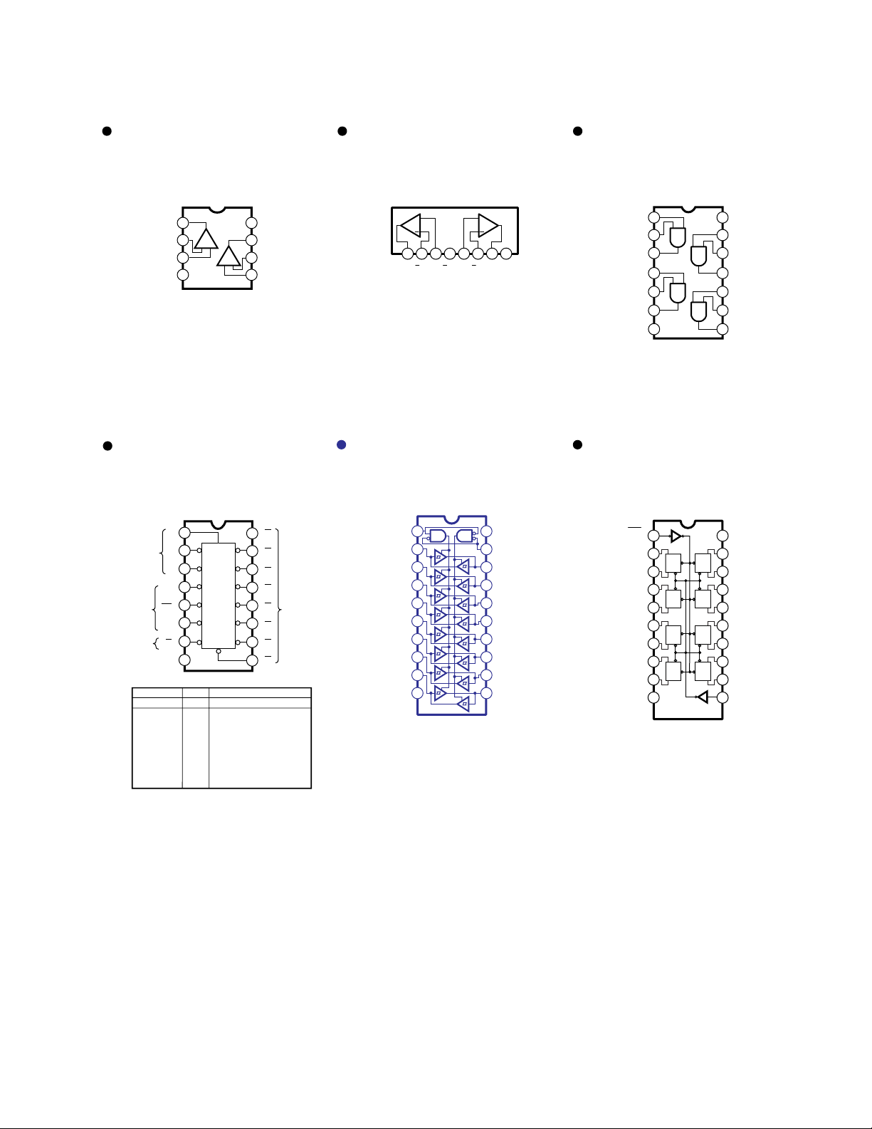
■ IC BLOCK DIAGRAM
LMY4-DA
NJM2068MD-T1 (XJ553A00)
Dual Operatinal Amplifier
DA: IC101, 102, 201, 202, 301, 302,
401, 402, 500, 600, 700, 800
+-
+DC Voltage
8
Supply
7
Output B
Inverting
6
Input B
Non-Inverting
5
Input B
Output A +V
Inverting
Input A
Non-Inverting
Input A
-DC Voltage Supply
1
2
3
4-V
+-
SN74LV138ANSR (IS013810)
DECODER
DA: IC003
1
A
2
B
B
Select
3
C
C
4
G2A G2A
5
G2B G2B
Enable
Output
ENABLEINPUTS
G1 G2A G2B C B A Y0 Y1 Y2 Y3 Y4 Y5 Y6 Y7
X
X
L
H
H
H
H
H
H
H
H
G1 G1
Y7 Y7
GND
H
X
X
H
X
X
L
L
L
L
L
L
L
L
L
L
L
L
L
L
L
L
6
7
8
SELECTINPUTS
X
X
X
X
X
X
X
X
X
L
L
L
H
L
L
L
H
L
H
H
L
L
L
H
H
L
H
L
H
H
H
H
H
16
A
Y6
Vcc
15
Y0Y0
14
Y1Y1
13
Y2Y2
12
Y3
Y3
Output
11
Y4Y4
10
Y5Y5
9
Y6
OUTPUTS
H
H
H
H
H
H
H
H
H
H
H
H
L
H
H
H
L
H
H
H
L
H
H
H
H
H
H
H
H
H
H
H
H
H
H
H
H
H
H
H
H
H
H
H
H
H
H
H
H
H
H
H
H
H
H
H
H
L
H
H
H
H
L
H
H
H
H
L
H
H
H
H
L
H
H
H
H
NJM4556AL (XP844A00)
Dual Operatinal Amplifier
DA: IC103, 203, 303, 403
+
1A2 3 4 5 6 7 8
IN V
+
IN
OUT
AAA
74VHC245SJX (XY874A00)
+
+
IN
BBB
B
OUT
+
VIN
Octal 3-State Bus Buffer
DA: IC001, 002, 004, 005, 008, 009
1D1R
2
A1
3
A2
4
A3
5
A4
6
A5
7
A6
8
A7
A8
9
GND
10
H
H
H
H
H
H
H
H
H
H
L
CC
V
20
OE
19
B1
18
B2
17
B3
16
B4
15
B5
14
B6
13
B7
12
B8
11
HD74LV08AFPEL (IS000800)
Qual 2 Input AND
DA: IC010
GND
1
2
1B
31A1Y
42A
52B
62Y
7 VSS
14
13
12
11 4Y
10 3B
93A
83Y
Vcc
4B
4A
HD74LV273AFPEL(IS027300)
Octal 3-State D-Type Flip Flop
DA: IC006
CLR
1
1Q
2
QQ
1D
DD
3
2D
4
D
QQ
2Q
5
3Q
6
QQ
D
3D
7
4D
8
DDCK
Q
4Q
9
10 11
CL CL
CK CK
CL
CL CL
CK
CL
Vcc
20
8Q
19
8D
18
7D
17
CK
DCK
CL
7Q
16
6Q
15
CK
D
6D
14
5D
13
CK
CL
Q
5Q
12
CLKGND
7
LMY4-DA
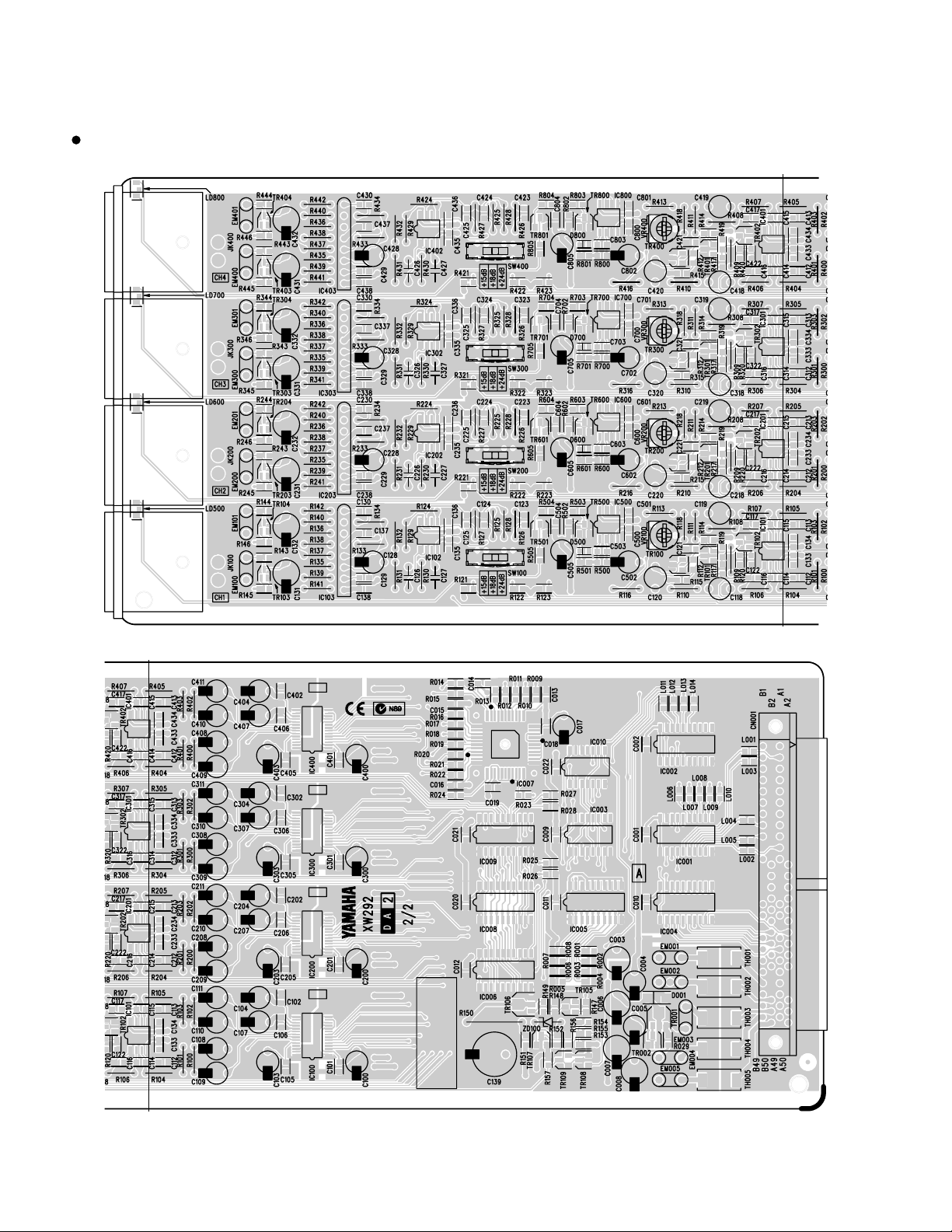
■ CIRCUIT BOARD
DA Circuit Board
GAIN SWITCH
SW100: CH1
SW200: CH2
SW300: CH3
SW400: CH4
A
A'
A'
A
Component side
DA: V412960
8
 Loading...