

Page 1

GX-505/GX-505VCD
MINI COMPONENT SYSTEM
GX-505
GX-505VCD
SERVICE MANUAL
GX-505 is composed of GX-505 (main unit) and NX-GX505s (speakers).
GX-505VCD is composed of GX-505VCD (main unit) and NX-GX505s (speakers).
IMPORTANT NOTICE
This manual has been provided for the use of authorized YAMAHA Retailers and their service personnel.
It has been assumed that basic service procedures inherent to the industry, and more specifically YAMAHA Products, are
already known and understood by the users, and have therefore not been restated.
WARNING: Failure to follow appropriate service and safety procedures when servicing this product may result in
IMPORTANT: The presentation or sale of this manual to any individual or firm does not constitute authorization, certifica-
The data provided is believed to be accurate and applicable to the unit(s) indicated on the cover. The research, engineering, and
service departments of YAMAHA are continually striving to improve YAMAHA products. Modifications are, therefore,
inevitable and specifications are subject to change without notice or obligation to retrofit. Should any discrepancy appear to
exist, please contact the distributor's Service Division.
WARNING: Static discharges can destroy expensive components. Discharge any static electricity your body may have
IMPORTANT: Turn the unit OFF during disassembly and part replacement. Recheck all work before you apply power to the
personal injury, destruction of expensive components, and failure of the product to perform as specified.
For these reasons, we advise all YAMAHA product owners that any service required should be performed
by an authorized YAMAHA Retailer or the appointed service representative.
tion or recognition of any applicable technical capabilities, or establish a principle-agent relationship
of any form.
accumulated by grounding yourself to the ground buss in the unit (heavy gauge black wires connect to this
buss).
unit.
GX-505/VCD
■ CONTENTS
TO SERVICE PERSONNEL ................................... 1—2
GX-505 PANELS ..................................................... 3—4
GX-505VCD PANELS ...................................................5
SPECIFICATIONS ......................................................... 6
INTERNAL VIEW .......................................................... 7
DISASSEMBLY PROCEDURES .......................... 8—12
VOLUME RANGE ....................................................... 13
SYSTEM CONTROL CHECK ..................................... 13
TEST MODE ................................................................ 14
SYSTEM TEST MODE................................................ 14
RECEIVER TEST MODE .................................... 15—16
TAPE TEST MODE .....................................................16
CD TEST MODE .........................................................17
100714
ALL FUNCTION TEST MODE.................................... 18
CD ERROR MESSAGES ............................................18
CD STANDARD OPERATION CHART .............. 19—20
ADJUSTMENTS .................................................. 21—23
IC DATA .............................................................. 24—30
DISPLAY DATA .................................................. 31—32
BLOCK DIAGRAM .............................................. 33—37
PRINTED CIRCUIT BOARD ............................... 38—60
PIN CONNECTION DIAGRAM ................................... 61
SCHEMATIC DIAGRAM ..................................... 62—69
PARTS LIST ...................................................... 70—102
GX-505 REMOTE CONTROL TRANSMITTER ........103
GX-505VCD REMOTE CONTROL TRANSMITTER ....
104
Page 2
GX-505/GX-505VCD
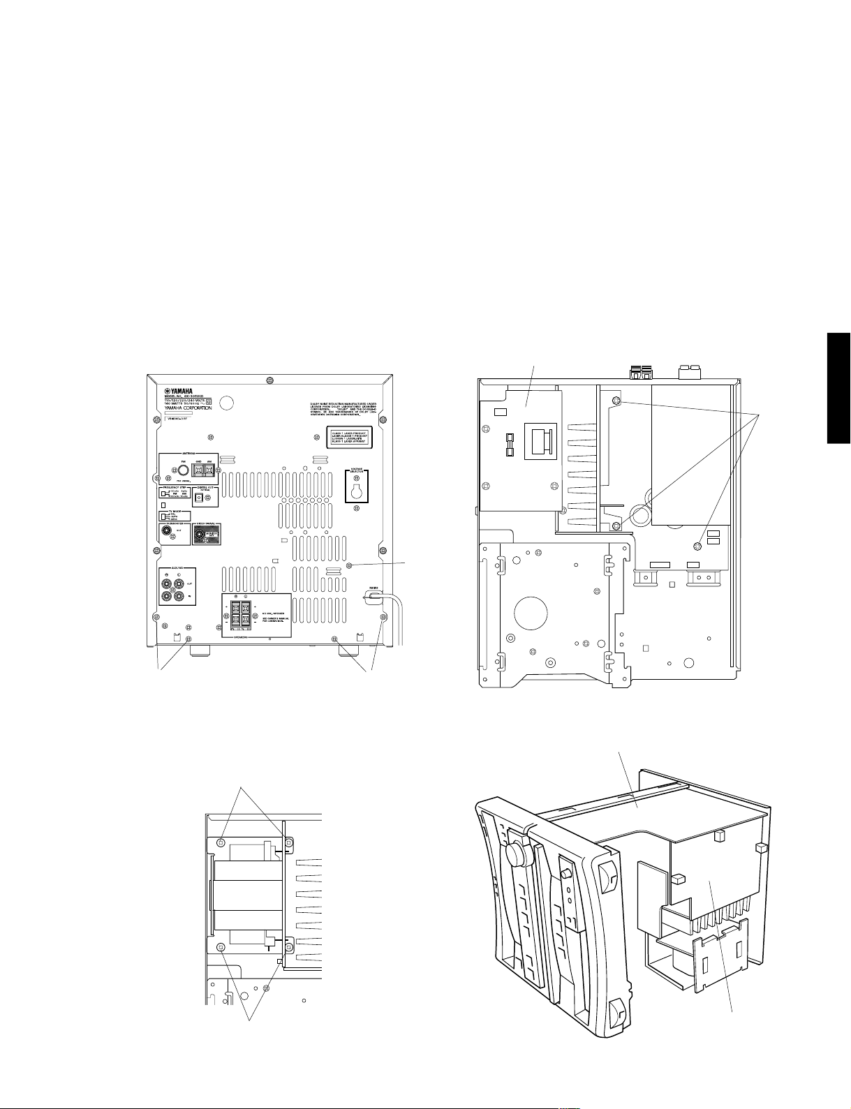
■ TO SERVICE PERSONNEL
1. Critical Components Information.
Components having special characteristics are marked Z
and must be replaced with parts having specifications equal
to those originally installed.
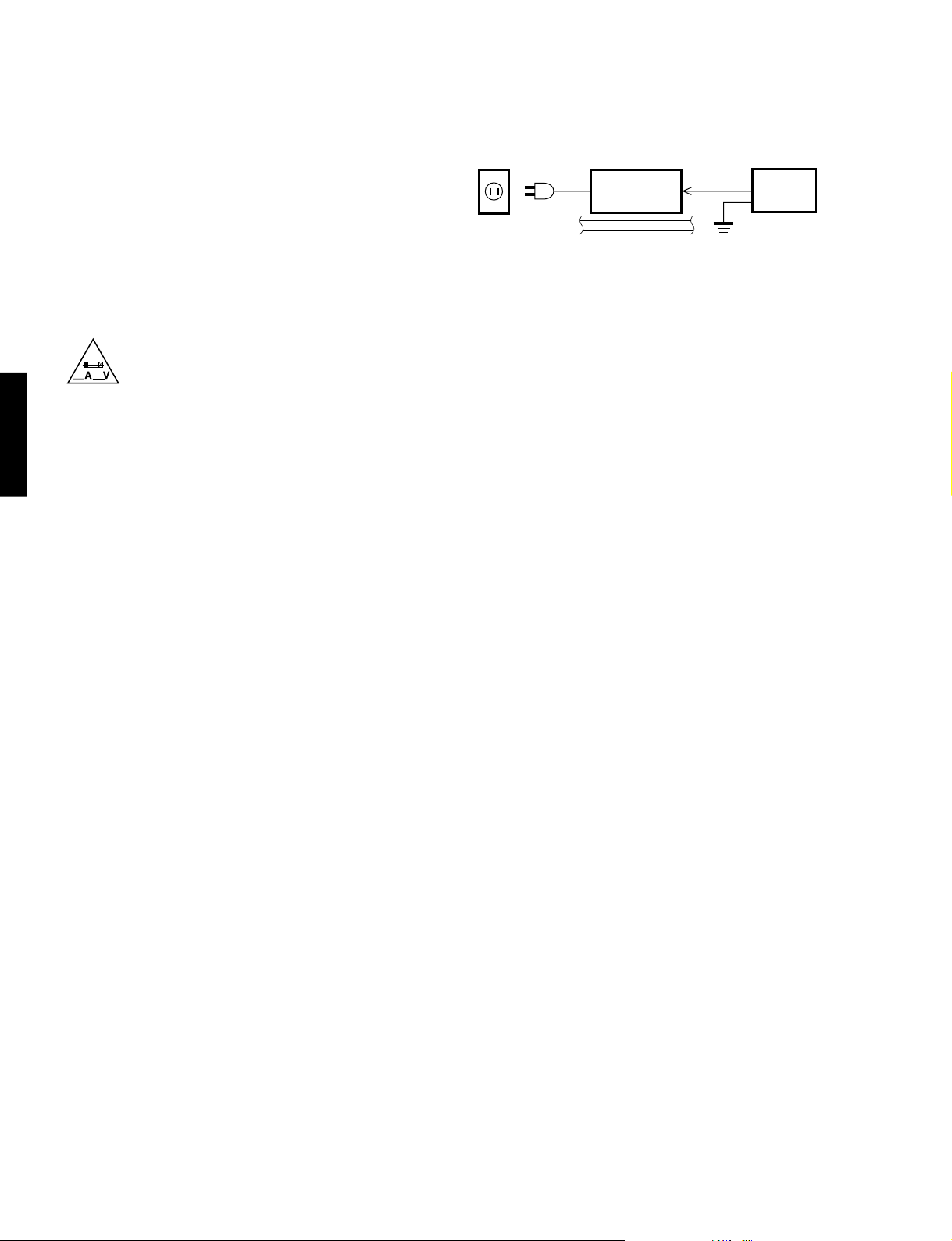
2. Leakage Current Measurement (For 120V Models Only).
When service has been completed, it is imperative to verify
that all exposed conductive surfaces are properly insulated
from supply circuits.
● Meter impedance should be equivalent to 1500 ohm shunted
by 0.15µF.
“CAUTION”
“F201 : FOR CONTINUED PROTECTION AGAINST RISK OF FIRE, REPLACE ONLY WITH SAME TYPE 2.0A, 125V FUSE.”
“F202 : FOR CONTINUED PROTECTION AGAINST RISK OF FIRE, REPLACE ONLY WITH SAME TYPE 4.0A, 125V FUSE.”
CAUTION
F201 : REPLACE WITH SAME TYPE 2.0A, 125V FUSE.
F202 : REPLACE WITH SAME TYPE 4.0A, 125V FUSE.
ATTENTION
GX-505/VCD
F201 : UTILISER UN FUSIBLE DE RECHANGE DE MEME TYPE DE 2.0A, 125V.
F202 : UTILISER UN FUSIBLE DE RECHANGE DE MEME TYPE DE 4.0A, 125V.
WARNING: CHEMICAL CONTENT NOTICE!
WALL
OUTLET
● Leakage current must not exceed 0.5mA.
● Be sure to test for leakage with the AC plug in both
polarities.
EQUIPMENT
UNDER TEST
INSULATING
TABLE
AC LEAKAGE
TESTER OR
EQUIVALENT
The solder used in the production of this product contains LEAD. In addition, other electrical/electronic and/or
plastic (where applicable) components may also contain traces of chemicals found by the California Health and
Welfare Agency (and possibly other entities) to cause cancer and/or birth defects or other reproductive harm.
DO NOT PLACE SOLDER, ELECTRICAL/ELECTRONIC OR PLASTIC COMPONENTS IN YOUR MOUTH FOR
ANY REASON WHATSOEVER!
Avoid prolonged, unprotected contact between solder and your skin! When soldering, do not inhale solder fumes
or expose eyes to solder/flux vapor!
If you come in contact with solder or components located inside the enclosure of this product, wash your hands
before handling food.
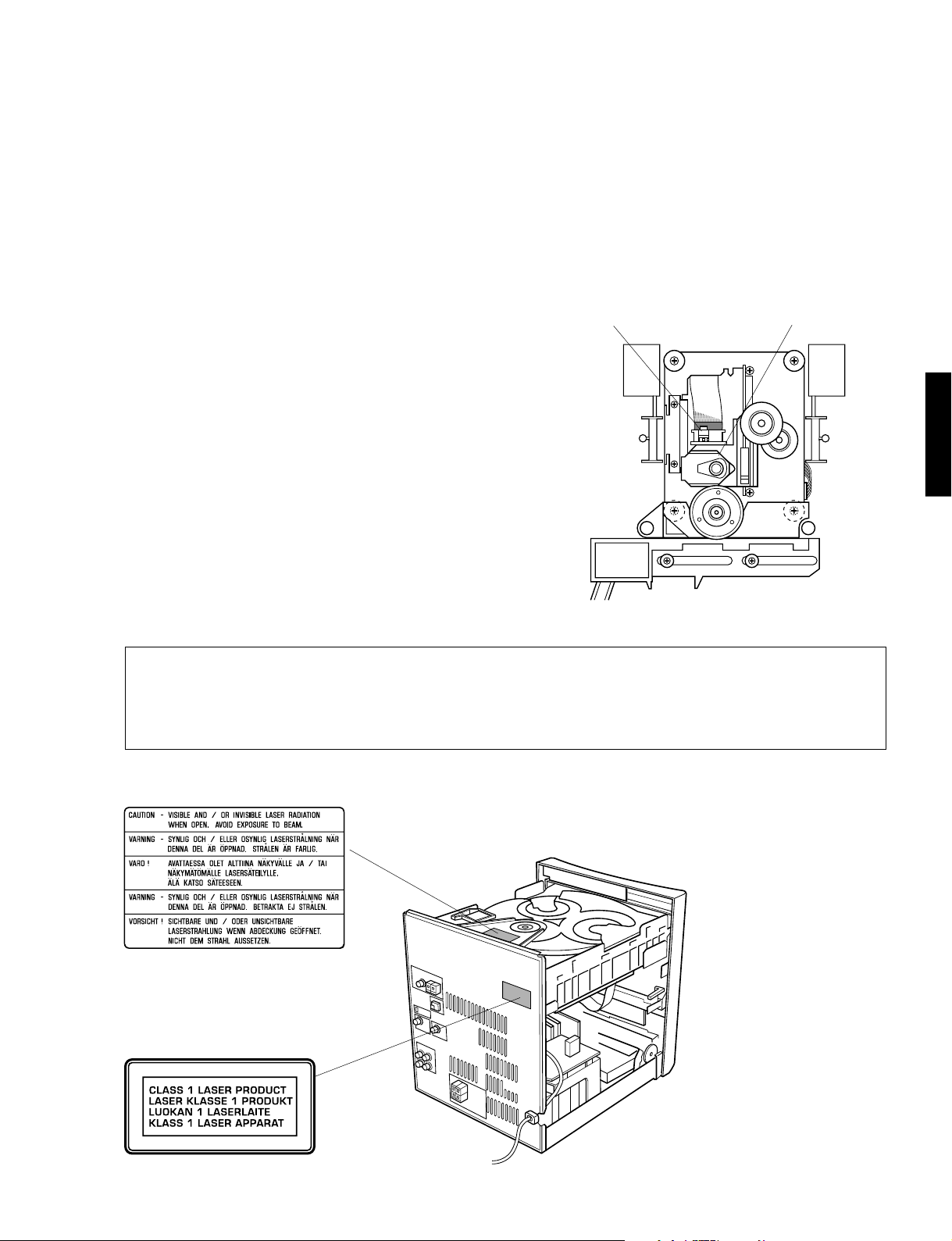
WARNING: Laser Safety
This product contains a laser beam component. This component may emit invisible, as well as visible radiation,
which may cause eye damage. To protect your eyes and skin from laser radiation, the following precautions must
be used during servicing of the unit.
1) When testing and/or repairing any component within the product, keep your eyes and skin more than 30 cm away from
the laser pick-up unit at all times. Do not stare at the laser beam at any time.
2) Do not attempt readjustment, disassembly or repair of the laser pick-up, unless noted elsewhere in this manual.
3) CAUTION : Use of controls, adjustments or performance of procedures other than those specified herein may result in
hazardous radiation exposure.
1
Page 3
GX-505/GX-505VCD
Laser Emitting conditions:
1) When the Top Cover is removed, and the STANDBY SW is turned to the "ON" position, the laser component will emit
a beam for several seconds to detect if a disc is present. During this time (5-10 sec.) the laser may radiate through the
lens of the laser pick-up unit. Do not attempt any servicing during this period!
If no disc is detected, the laser will stop emitting the beam. When a disc is set, you will not be exposed to any laser
emissions.
2) The laser power level can be adjusted with the VR on the pick-up PWB, however, this level has been set by the factory
prior to shipping from the factory. Do not adjust this laser level control unless instruction is provided elsewhere in this
manual. Adjustment of this control can increase the laser emission level from the device.
Variable resistor
Laser Diode Properties
Material : GaAlAs
Wavelength : 780 nm
Emission duration : Continuous
Laser output : Max. 44.6µW*
ANSI Class : Class 1
* This output is the value measured at a distance of about
200 mm from the objective lens surface on the Optical Pickup Block.
VARO! : AVATTAESSA JA SUOJALUKITUS OHITETTAESSA OLET ALTTIINA NÄKYMÄTTÖMÄLLE
LASER-SÄTEILYLLE. ÄLÄ KATSO SÄTEESEEN.
VARNING! : OSYNLIG LASERSTRÅLNING NÄR DENNA DEL ÄR ÖPPNAD OCH SPÄRREN ÄR URKOPPLAD.
BETRAKTA EJ STRÅLEN.
(Do not turn)
Optical pick-up
GX-505/VCD
B, G, R, L, T models
B, G, R, L, T models
2
Page 4
GX-505/GX-505VCD
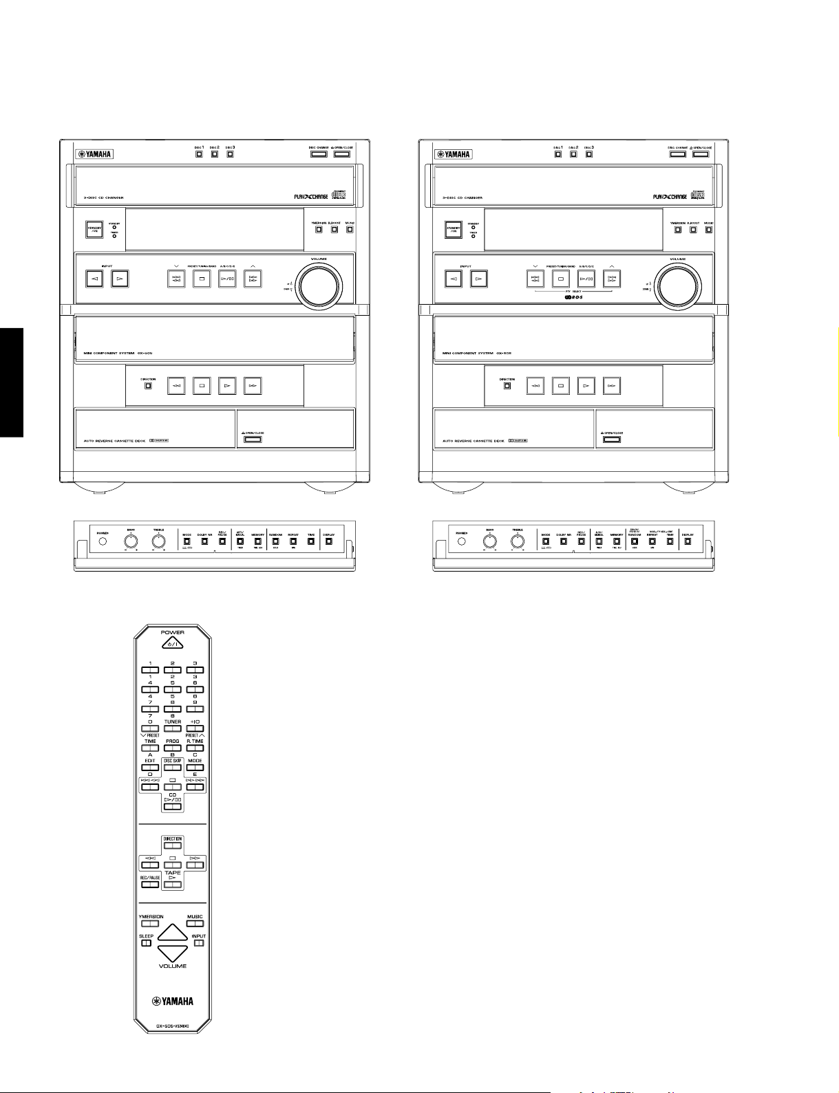
■ GX-505 PANELS
▼ U, C, R, A models
GX-505/VCD
▼ B, G models
3
Page 5
GX-505/GX-505VCD
▼ U, C models
▼ R model
GX-505/VCD
▼ A model
▼ B, G models
4
Page 6

GX-505/GX-505VCD
■ GX-505VCD PANELS
GX-505/VCD
▼ R, T models
▼ L model
5
Page 7
■ SPECIFICATIONS
GX-505/GX-505VCD
■ AMPLIFIER SECTION
Minimum RMS Output Power per Channel
1kHz, 0.9% THD, 6Ω .................................................. 80W + 80W
1kHz, 10% THD, 6Ω ............................................... 100W + 100W
Input Sensitivity/Impedance
AUX/MD......................................................................200mV/47kΩ
Spectrum Analyzed Band ........................................................... 5 band
(100Hz, 350Hz, 1kHz, 3.5kHz, 10kHz)
■ VIDEO SECTION (GX-505VCD only)
Signal Level ............................................................................ 1Vp-p/75Ω
■ TUNER SECTION
FM Tuning Range
U, C models .......................................................87.5 to 107.9MHz
R, T models ...................... 87.5 to 108.0MHz/87.50 to 108.00MHz
A, B, G, L model ............................................ 87.50 to 108.00MHz
AM Tuning Range
U, C models .........................................................530 to 1,710kHz
R, T models .............................. 530 to 1,710kHz/531 to 1,611kHz
A, B, G, L models.................................................531 to 1,611kHz
FM Usable Sensitivity (75Ω)
30dB S/N Quieting, Mono, 1kHz,
100% mod. R, U, C, L, T models...................... 1.5µV (14.8dBf)
DIN Mono, S/N 26dB (A, B, G only) ..................................... 1.8µV
■ CD CHANGER SECTION
Type ........................................................ 3-Disc Carousel Auto-changer
Signal Readout.................................................................... Non-contact,
3-beam semi-conductor laser pick-up
D/A Converter............................................................................1bit DAC
Filter ..................................................... 8-time oversampling digital filter
Wow & Flutter .................................................................. Unmeasurable
■ TAPE DECK SECTION
Type ................................................................................... Auto Reverse
Heads
4-Track 2-Channel playback/recording stereo Cassette Deck
REC/PB .................................................................. Hard permalloy
Erase ............................................................... Double Gap Ferrite
Motors
Main ....................................................................... DC servo motor
Tray Loading....................................................................DC motor
Wow & Flutter
W.PEAK.............................................................................. ±0.19%
W.RMS ................................................................................. 0.09%
Frequency Response (–20dB)
Type I/Normal tape ..................................... 50 to 15,000Hz ± 3dB
Type II/High (CrO2) tape............................. 50 to 16,000Hz ± 3dB
S/N Ratio
NR off ..................................................................................... 58dB
Dolby B NR on ....................................................................... 66dB
■ SPEAKER SECTION (NX-GX505)
Type .............................................................. 3-Way Bass-reflex Design
(Magnetic-Shielding Type)
Speakers ................................................................. 13cm (5-1/8”) woofer
5cm (1-15/16”) tweeter
2cm (13/16”) super tweeter
Frequency Range............................................................ 60 to 27,000Hz
Maximum Input .............................................................................. 220W
Impedance ........................................................................................... 6Ω
Frequency Range............................................................ 60 to 27,000Hz
Sound Pressure Level.................................. 90dB/1m • 2.83V (1W/6Ω)
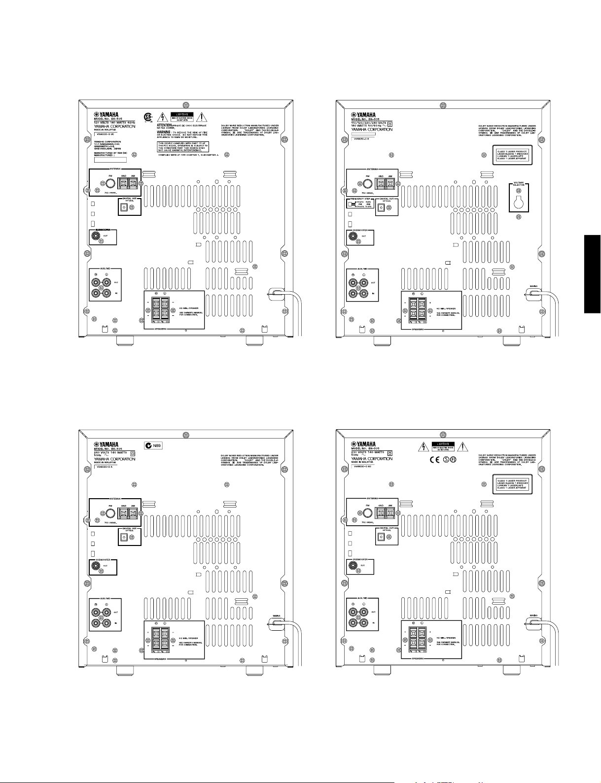
■ GENERAL
Power Supply
U, C models ............................................................ AC120V, 60Hz
A model ...................................................................AC240V, 50Hz
B, G, L models ........................................................AC230V, 50Hz
R, T models ...................................AC110/120/220/240V, 60/50Hz
Power Consumption ...................................................................... 140W
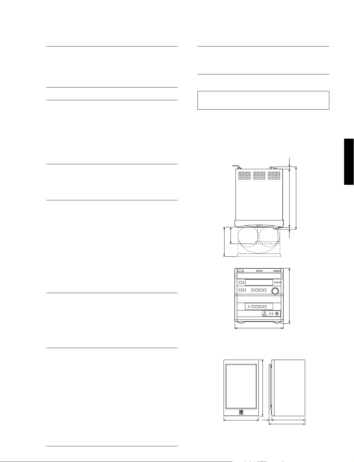
Dimensions (W X H X D)
(approx. 1.3W when set to the standby mode)
GX-505/GX-505VCD ..................................... 280 X 320 X 365mm
NX-GX505 ..................................................... 200 X 320 X 208mm
(11” X 12-5/8” X 14-3/8”)
(7-7/8” X 12-5/8” X 8-3/16”)
Weight
GX-505/GX-505VCD ..................................... 10.2kg (22 lbs. 7 oz)
NX-GX505 ................................................ 3.8kg (8 lbs. 6 oz)/each
Finish
GX-505 .......................................................................... Silver color
GX-505VCD ...................................................................Silver color
NX-GX505 ................................................ Cherry color/Black color
Accessories ........................................................... AM loop antenna X 1
Indoor FM antenna X 1
Remote Control Transmitter X 1
Battery (size “AA”, R06) X 2
Speaker Cord (5m) X 2
* Specifications subject to change without notice.
* Manufactured under license from Dolby Laboratories Licensing
Corporation. “DOLBY” and the double-D symbol V are
trademarks of Dolby Laboratories Licensing Corporation.
U ......................... U.S.A. model G .................. European model
C ................... Canadian model R ...................... General model
A .................. Australian model L.................. Singapore model
B ........................ British model T .......................... China model
● GX-505/GX-505VCD
12
(1/2")
339 (13-3/8")
365 (14-3/8")
100
172 (6-3/4")
(3-15/16")
280 (11")
14
(9/16")
320 (12-5/8")
● NX-GX505
320 (12—15/8")
200 (7—7/8")
(1/16")
192 (7—9/16")15.8
207.8 (8—3/16")
Unit : mm (inch)
GX-505/VCD
6
Page 8
GX-505/GX-505VCD
■ INTERNAL VIEW
q
GX-505/VCD
Top side
w
(with CD/VCD Mechanical Unit removed)
e r t
i
oy u
q TUNER P.C.B.
w MAIN P.C.B. (5)
e MAIN P.C.B. (1)
r INPUT P.C.B. (1)
t OPERATION P.C.B. (3)
(GX-505VCD only)
y MAIN P.C.B. (2)
u MAIN P.C.B. (3)
i MAIN P.C.B. (6)
o DECK MECHANICAL UNIT
!0 GX-505 INPUT P.C.B. (3)
GX-505VCD INPUT P.C.B. (2)
!1 GX-505 CD MECHANICAL UNIT
GX-505VCD VCD MECHANICAL UNIT
!2 GX-505 CD P.C.B.
GX-505VCD VCD P.C.B.
!3 VCD MODULE (GX-505VCD only)
Left side
!1!0 q
!2 !3
u i
7
y
ro
Page 9
GX-505/GX-505VCD
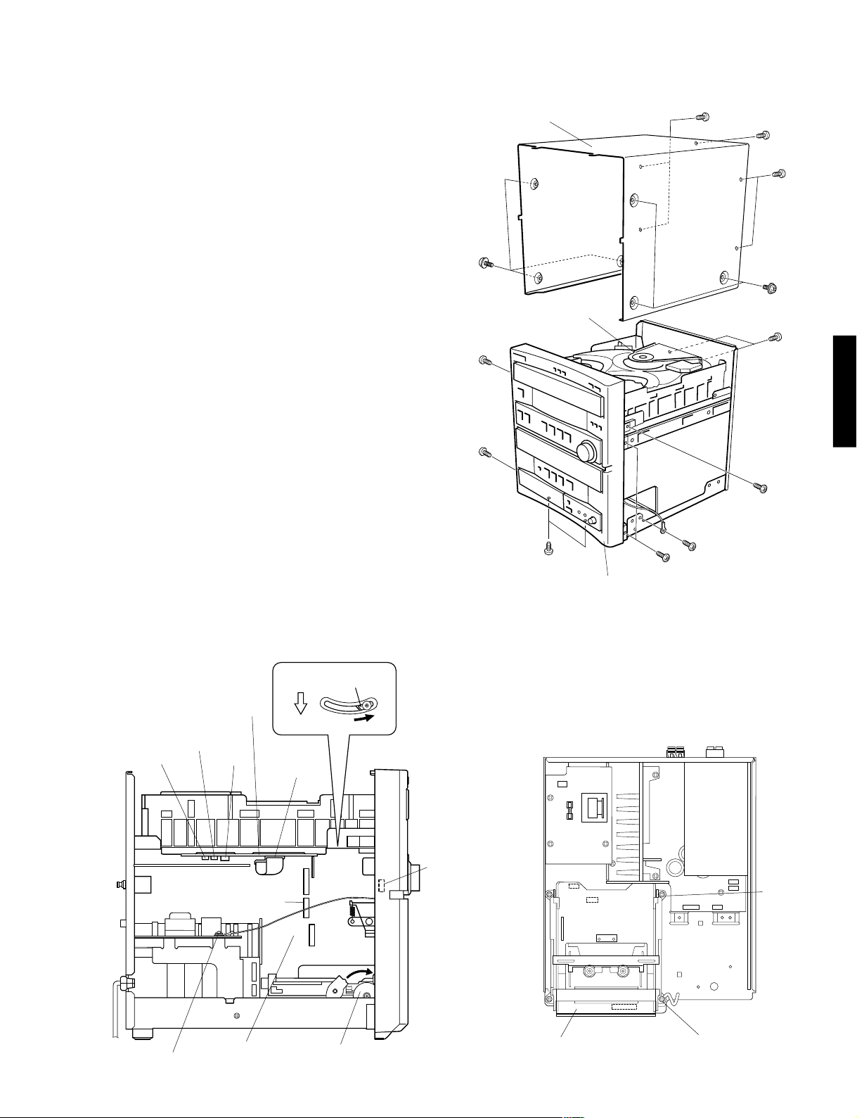
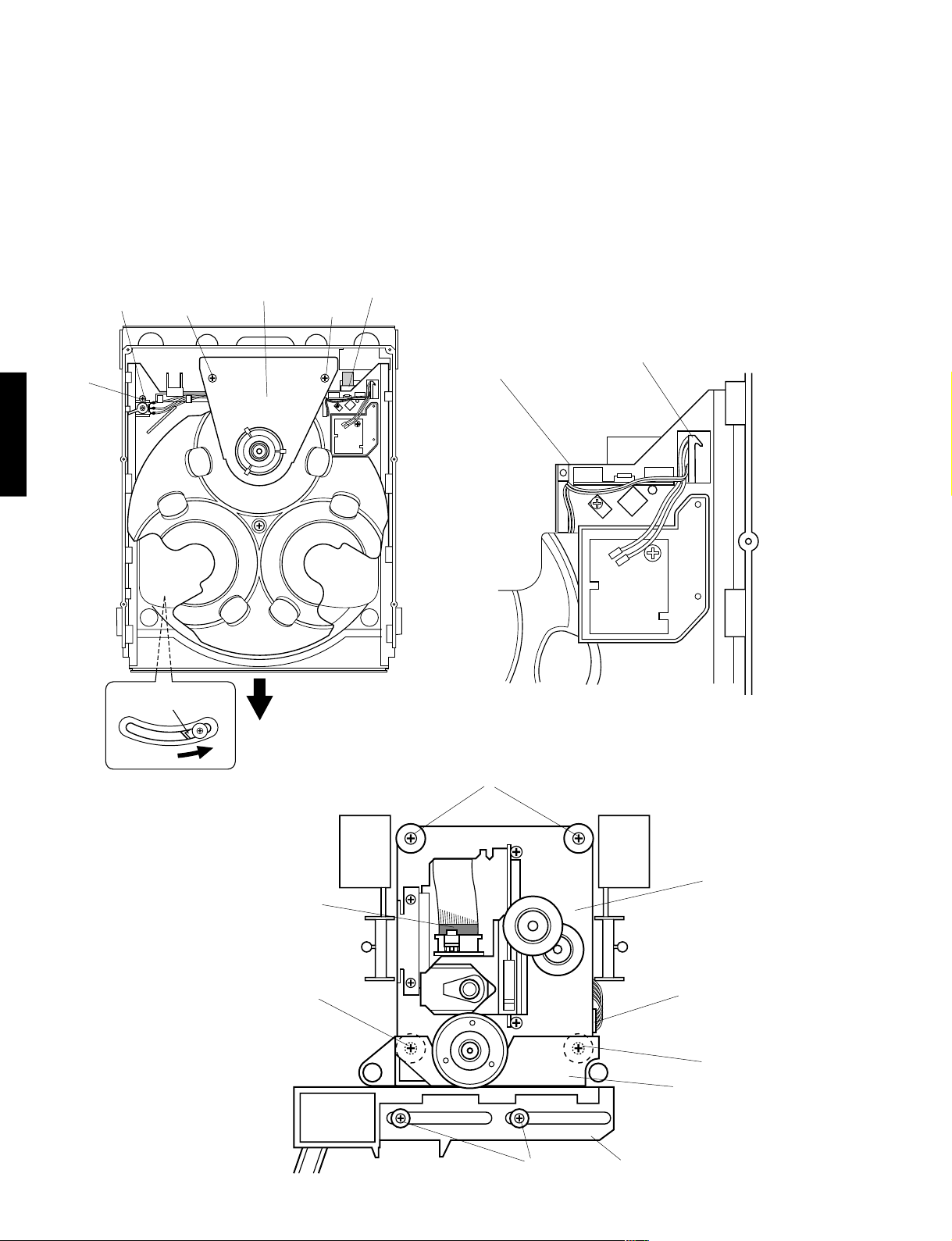
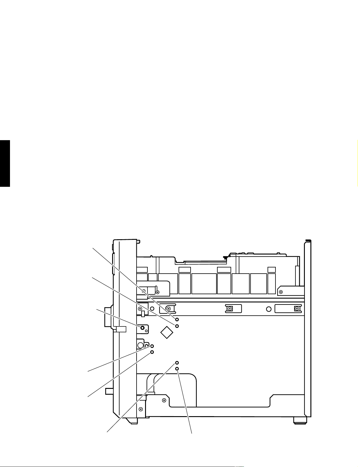
■ DISASSEMBLY PROCEDURES (Remove parts in the order as numbered.)
1. Removal of Top Cover
Remove 11 screws ( q ) in Fig. 1.
Top Cover
q
q
2. Removal of CD/VCD Mechanical Unit
a. Disconnect the power cord from the AC outlet.
b. Push the Friction Arm ( the bottom side of the CD/
VCD Mechanical Unit ) with a finger as shown in Fig.
2.
c. Pull the Tray forward approx. 5cm ( 2" ) and remove
the CD Lid in Fig. 2.
d. Push the Tray back to the original, closed position.
e. Disconnect the Flat Connecting Cables ( CB10 ) on the
CD/VCD P.C.B. and remove 3 connectors ( CB11 ,
CB12 and CB9 ) on the CD/VCD P.C.B. in Fig. 2.
f. Remove 4 screws ( w ) and then remove the CD
Mechanical Unit in Fig. 1.
3. Removal of Panel Unit
a. Rotate the Loading Gear, then open the Tray and
remove the Cassette Lid in Fig. 2.
b. Push the Tray back to the original, closed position.
c. Disconnect the flat connecting cables ( CB10, CB13
and CB11 ) on the INPUT P.C.B. and remove a
connector ( CB805 ) in Fig. 2.
d. Remove 5 screws ( e ) and 2 screws ( r ), and then
remove the Panel Unit in Fig. 1 and Fig. 2.
Friction
Arm
q
q
CD/VCD Mechanical Unit
w
e
w
r
e
e
Panel Unit
Fig. 1
4. Removal of Deck Mechanical Unit
a. Remove 4 screws ( t ) and then remove the Deck
Mechanical Unit in Fig. 3.
b. Remove 3 connectors ( W2, W3 and W4 ) in Fig. 3.
q
w
GX-505/VCD
CB11
CD/VCD P.C.B.
CB12
(VCD only)
r
CB9
CB11
(VCD only)
INPUT P.C.B.
FRONT
CB10
CB13
CB10
Loading Gear
CD Lid
Cassette Lid
Fig. 2
CB805
W2
t
t
Deck Mechanical Unit
W4
W3
t
t
Fig. 3
8
Page 10
GX-505/GX-505VCD
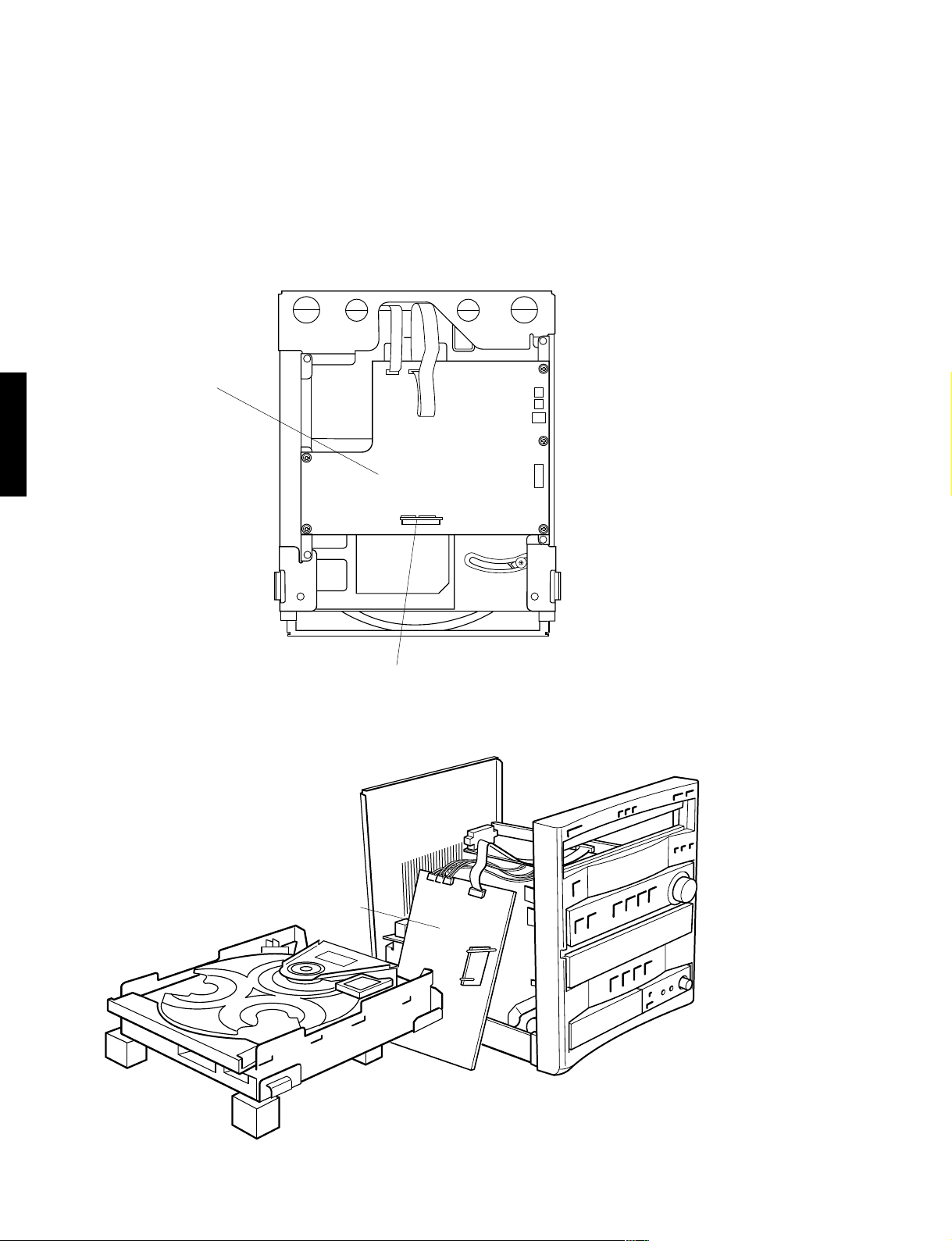
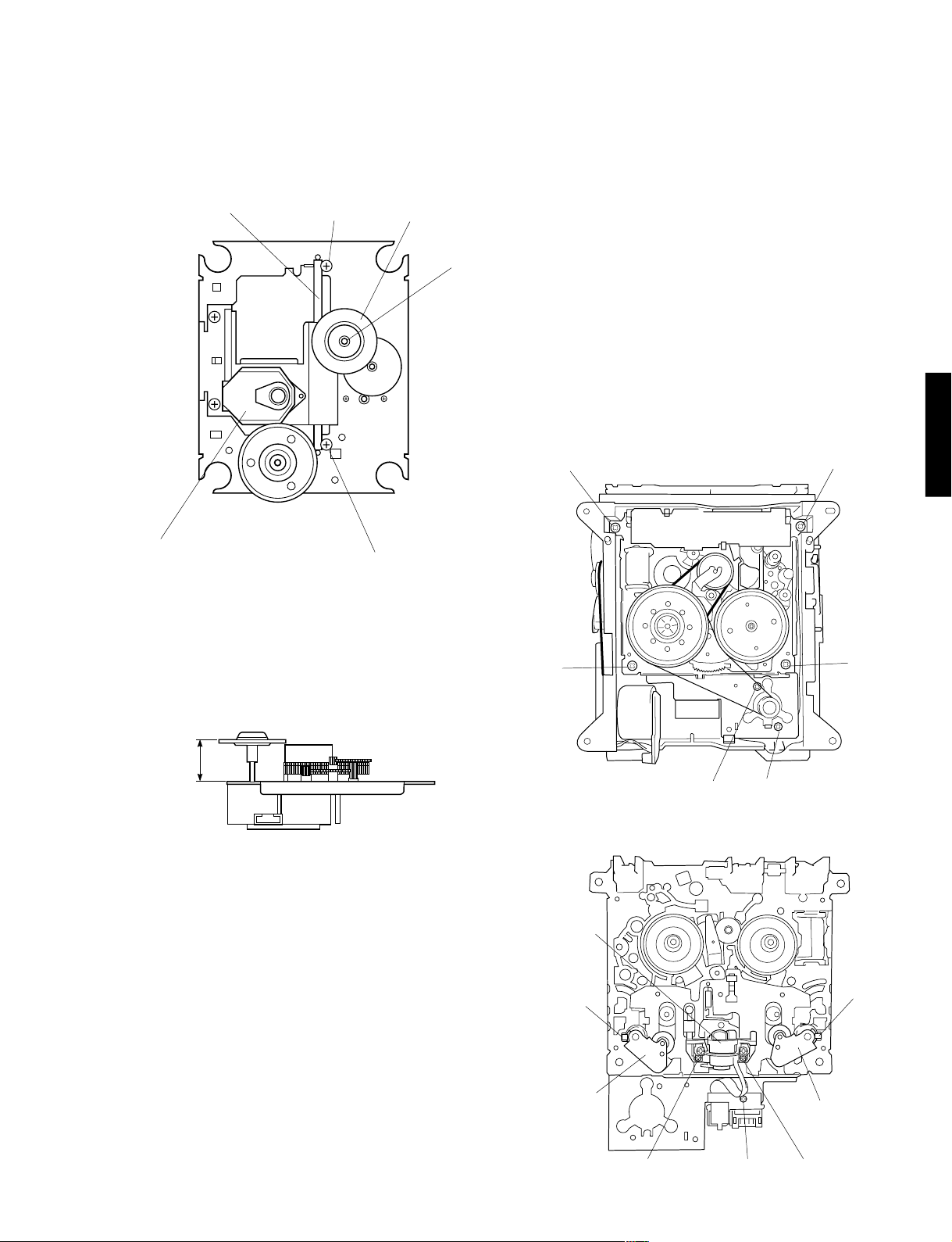
5. Operation Check of CD/VCD P.C.B.
a. Remove the CD Mechanical Unit.
b. Remove 5 screws ( y ) and then remove the CD/VCD P.C.B. in Fig. 4.
c. Place blocks (at 3 locations) to hold the CD Mechanical Unit horizontally as
shown in the Fig. 5.
d. Connect the Flat Connecting Cable ( CB10 ) and 3 connectors ( CB11,
CB12 and CB9 ) in Fig. 4 and Fig. 5.
e. Fit insulating material (thick paper, etc.)to prevent the chassis from
contacting the CD/VCD P.C.B.
f. Connect the power plug and turn on the Power Switch.
GX-505/VCD
CD/VCD P.C.B.
y
CB11
CB12 (VCD only)
CB9
y
y
CB10
y
VCD Module
(GX-505VCD only)
y
Fig. 4
CD/VCD P.C.B.
Block
Block
Block
Fig. 5
9
Page 11
GX-505/GX-505VCD
6. Operation Check of Main P.C.B. (1)
a. Remove the CD Mechanical Unit.
b. Remove the Panel Unit.
c. Remove the Deck Mechanical Unit.
d. Remove 5 screws ( u ) in Fig. 6.
e. Remove 1 screw ( i ) and then remove the Main P.C.B. (2) in Fig. 7.
f. Remove 3 screws ( o ) in Fig. 7.
g. Remove 4 screws ( !0 ) and then remove the Power Transformer in Fig. 8.
h. Place the main unit on its left side (viewed from the front) and remove the Bottom Cover in Fig. 9.
i. Install the Panel unit to the main unit in Fig. 9.
j. Connect the flat connecting cables ( CB10, CB13 and CB11 ) and remove a connector ( CB805 ) in Fig. 2.
k. Connect the power plug and turn on the Power Switch.
CAUTION
When the power to this equipment is turned on with the CD/VCD Mechanical Unit disconnected, the capacitor C255(4700/
16) of the Main P.C.B. (CD/VCD power supply section) is charged. Connecting the CD/VCD P.C.B. in this state may cause
damage to its IC. Therefore, when installing the CD/VCD Mechanical Unit, be sure to discharge the capacitor C255(4700/
16) of the Main P.C.B. before making connections. (To discharge it, short the W201 terminal +B and GND with a
resistor(270Ω 1W).)
Main P.C.B. (2)
GX-505/VCD
o
i
u
uu
Fig. 6
!0
Fig. 7
Input P.C.B.
!0
Fig. 8
Main P.C.B. (1)
Fig. 9
10
Page 12
GX-505/GX-505VCD
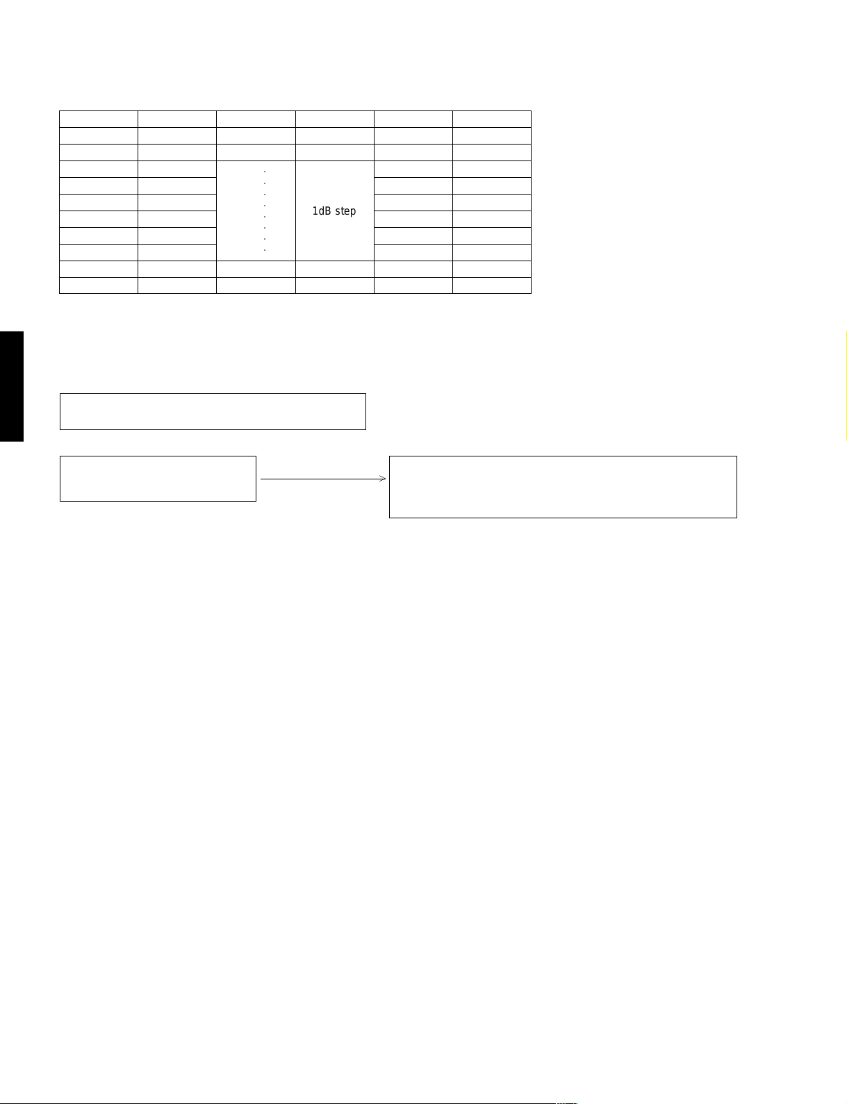
7. Removal of Tray & Traverse Unit
a. Remove 2 screws ( !1 ) and then remove the Clamper Bracket in Fig. 10.
b. Remove 1 screw ( !2 ) and then remove the Lever Switch in Fig. 10.
c. Disconnect the Flat Connecting Cable ( 9P ) in Fig. 10.
d. Push the Friction Arm ( the bottom side of the CD Mechanical Unit ) with a screwdriver or the like and pull out the Tray
forward as in Fig. 10.
e. Unhook 1 Tray hook in Fig. 11 and pull out the Tray.
f. Remove 4 screws ( !3 and !4 ) in Fig. 12.
g. Disconnect the Flat Connecting Cable ( 16P ) and connectors ( 6P ).
h. Take out the Traverse Unit with the Slider Cam and the TU Holder in Fig. 12.
i. Remove 2 screws ( !5 ) and then remove the TU Holder in Fig. 12.
Lever Switch
(OPEN/CLOSE)
!2
GX-505/VCD
Friction
Arm
Clamp Bracket
!1
CN3(9P)
!1
Tray
Fig. 10
Hook
Fig. 11
11
16P
!5
!4
Traverse Unit
6P
!5
TU Holder
!3
Slider Cam
Fig. 12
Page 13
GX-505/GX-505VCD
8. Removal of Pick-up Head
a. Remove a washer ( !6 ) and then remove the Driving
Gear in Fig. 13.
b. Remove 2 screws ( !7 ), pull out the Guide Rod and
then remove the Pick-up Head in Fig. 13.
Guide Rod
!7
Driving Gear
!6
9. Removal of Cassette Mechanism
Remove 4 screws ( !8 ) and then pull out the Cassette
Mechanism in Fig. 14.
10. Removal of Main Motor
Remove 2 screws ( !9 ) in Fig. 14.
11. Removal of Pinch Roller
Detach the hook and then remove the Pinch Roller
in Fig. 15.
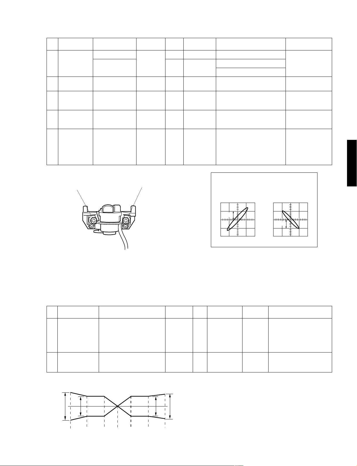
12. Removal of Head Ass’y
a. Remove 1 screw ( @0 ) and then remove the Relay
P.C.B. in Fig. 15.
b. Remove 2 screws ( @1 ) and then remove the Head
Ass’y in Fig. 15.
* Perform the azimuth adjustment after installing the
Head Ass’y.
!8
!8
GX-505/VCD
Pick-up Head
!7
Fig. 13
● Check that the disc table height is as specified below.
19.4 ± 0.2 mm
Fig. A
!8
Head Ass'y
Hook
!9
!8
!9
Fig. 14
Hook
Pinch Roller (L)
@0@1 @1
Pinch Roller (R)
Fig. 15
12
Page 14
GX-505/GX-505VCD
■ VOLUME RANGE
DISPLAY
VOL MIN
VOL 01
VOL 02
VOL 03
VOL 04
VOL 05
VOL 06
VOL 07
VOL 08
VOL 09
NOTE) When VOLUME is at minimum, AMP MUTE is on.
dB
– ∞
–79
–73
–68
–64
–61
–59
–58
–57
–56
DISPLAY
VOL 10
VOL 11
VOL 54
VOL 55
■ SYSTEM CONTROL CHECK
q FUNCTION AUX/MD is selected
GX-505/VCD
CD PLAY KEY ON (remote control transmitter)
↓
w FUNCTION → CD ?
DISC No. display on?
yes
↓
CHECK OK
○○○○○○○○
no
dB
–55
–54
1dB step
–11
–10
DISPLAY
VOL 56
VOL 57
VOL 58
VOL 59
VOL 60
VOL 61
VOL 62
VOL 63
VOL 64
VOL MAX
In case that CD doesn’t play : [RECEIVER → CD]
In case that DISPLAY doesn’t change : [CD → RECEIVER]
dB
–9
–8
–7
–6
–5
–4
–3
–2
–1
0
(SYSCK, CDCE, SYSO) NG
(SYSI) NG
SYSCK: Pin 20 of IC8
CDCE: Pin 25 of IC8
SYSO: Pin 21 of IC8
SYSI: Pin 22 of IC8
13
Page 15
GX-505/GX-505VCD
■ TEST MODE
To facilitate inspection, measurement and location of any faulty point, 6 types of built-in Test Modes are provided,
one for each section.
• System Test Mode : Test mode for the system section. It is also used when entering the test mode for each section.
• Receiver Test Mode : Test mode for the receiver section
• Tape Test Mode : Test mode for the deck section
• CD Test Mode : Test mode for the CD section
• MD Test Mode : Test mode for the MD section (unused for this unit)
• All Function Test Mode : Test mode for all functions
■ SYSTEM TEST MODE
This test mode is used for the system section. Also, this mode must be executed first when entering the test mode
for each section.
Starting Procedure
In the STANDBY mode, press the STANDBY/ON button while pressing the RANDOM button and the PLAY/
PAUSE(CD) button simultaneously. Once the SYSTEM TEST MODE is set, causal factors for the previous power
off appear on the FL display.
Causal factors for power off at starting
Display Description
<Key Operate Power off by button operation
<Off Timer Power off by Off Timer setting
<Sleep Timer Power off by Sleep Timer function
<Auto Off Power off by Auto Power Off function
<I-Protect Power off by detection of an abnormal current value
<V-Protect Power off by detection of an abnormal voltage value
<Temp Over Power off by detection of an abnormal temperature value
<AC Cut Power off by AC power cut
<?? Unknown
Operation Procedure (Selection/finalizing of TEST MODE for each section)
1) Select the TEST MODE by the section name, pressing the wINPUT (up) or q INPUT (down) button.
GX-505/VCD
Display Description Ref. page
<Key Operate Causal factors for power off are displayed. 14
(This state is available immediately after starting.)
Test RECEIVER RECEIVER TEST MODE 15
Test TAPE TAPE TEST MODE 16
Test CD CD TEST MODE 17
Test MD MD TEST MODE (Unused for this unit) —
Test All Func ALL FUNCTION TEST MODE 18
Escape Test The test mode is canceled. —
2) Pressing the MUSIC button will shift the mode to the selected test mode.
For the details of the selected test mode, refer to the Ref. page in the above step 1).
14
Page 16

GX-505/GX-505VCD
■ RECEIVER TEST MODE
When the RECEIVER TEST MODE is set through the SYSTEM TEST MODE, “01 G.E.TEST” appears on the FL display.
(01 is the test program No.)
Test programs from 01 to 25 are incorporated in RECEIVER TEST MODE.
Operation Procedure (Selection/execution of Test Program)
1) Select the test program by pressing the rTAPE (up) or eTAPE (down) button.
2) Pressing the STANDBY/ON button will execute the selected test program.
3) Repeat selection/execution of the test program as necessary.
No. & DISPLAY
01 G , E , TEST
02 FL + CLEAR
GX-505/VCD
03 FL FULL
04 APO - ON/OFF
05 RDS - OFF/ON
06 A , PS - ON/OFF
07 A , M , - RDS/ALL
08 CT > C - ON/OFF
09 L > CT - ON/OFF
10 PSR2 - ON/OFF
11 RTBL - ON/OFF
12 SEC - OFF/ON
13 Temp
14 PEAK - ON/OFF
15 AMPC - OFF/ON
16 CDCH - ON/OFF
17 REM CODE
18 L , EN - ON/OFF
19 ALL CH >
20 RDS E / F
21 SUR TEST
22 KEYC - OFF/ON
23 AM - IF
24 CANCEL
25 DEST
FUNCTION
Equalizer check mode
FL display full lighting,
RAM CLEAR
FL display full lighting
Do not use No. 04 to 23 functions as they are not for servicing.
Used to cancel the test program.
(The normal operating mode is restored when the STANDBY/ON button is pressed.)
Destination display mode
Used to check EQ.
Pressing the STANDBY/ON button will set the Equalizer Test mode.
For the details, refer to page 16.
Used for lighting of all display segments and clearing of RAM. (Note that
the user memory will be cleared.)
At the first pressing of the STANDBY/ON button, all display segments light up
and at the second pressing, MEMORY and M-CLEAR light up for 2 seconds
and RAM of CPU is initialized. (The normal operating mode is restored.)
(Presetting of the tuner becomes the manufacturer preset state.)
Used to check lighting of all display segments.
At the first pressing of the STANDBY/ON button, all display segments light up and at the
second pressing, this mode is canceled. (The normal operating mode is restored.)
PURPOSE & OPERATION
15
Page 17
GX-505/GX-505VCD
Equalizer test mode (Test program No. 01)
When the equalizer test mode is set, “GEQ - xxx” is displayed. “xxx” represents the 3 band value of GEQ.
It is possible to set the GEQ value directly, using the buttons on the remote control unit.
Example : To obtain flat
GEQ - 6 6 6
Low tone Intermediate tone High tone
Displayed value 0 123456789ABC
Gain (dB) -12 -10 -8 -6 -4 -2 0 +2 +4 +6 +8 +10 +12
Operation Procedure
• To set a value for each band
[ 0 ] to [ 9 ], [ A(TIME) ], [ B(PROG) ], [ C(R.TIME)]
• To set all bands to Min (-12dB)
[ D(EDIT) ]
• To set all bands to Max (+12dB)
[ E(+10) ]
• To cancel this test mode, press the STANDBY/ON button. (The normal operating mode will be restored.)
GX-505/VCD
● FACT0RY PRESET
BAND
FM (MHz)
AM (kHz)
NOTE 1) PRESET PAGE ............................................ A : FM B : AM C : FM D : AM E : FM
U, C, R, T (100k/10k)
A, B, G, L, R, T (50k/9k)
U, C, R, T (100k/10k)
A, B, G, L, R, T (50k/9k)
MARKETS
1
98.1
98.10
630
630
2
95.1
95.10
1080
1080
3
87.5
87.50
1400
1404
PRESET No.
4
101.5
101.50
530
531
5
107.9
108.00
1710
1611
6
88.1
88.10
900
900
7
106.1
106.10
1350
1350
8
107.9
107.90
1440
1440
CAUTION : When executing Test program No. 2 RAM CLEAR, be sure to write down the preset memory contents of the
tuner, using a table like the one shown below. Execution of RAM CLEAR will set the memory contents of the
tuner back to the factory preset state which means that all the memories preset by the user will be erased.
Preset group
A
B
C
D
E
P1 P2 P3 P4 P5 P6 P7 P8
■ TAPE TEST MODE
When the TAPE TEST MODE is set through the SYSTEM TEST MODE, “Tape Test XXXX” appears on the FL display.
(XXXX is the counter value.)
The operating condition of the deck section will be as follows.
• When the reverse mode is set to “endless”, the number of playback repetition becomes unlimited.
(It is set to “8” times in the normal operating mode.)
• When in the REC mode, AUX/MD is used automatically for the input source.
16
Page 18

GX-505/GX-505VCD
■ CD TEST MODE
When the CD TEST MODE is set through the SYSTEM TEST MODE, “00 TM1 00: 00” appears on the FL display.
The CD TEST MODE is enabled. Each button operates as follows for each mode. The MODE No. is increased by
pushing
"+10" button.
Button
" 0 "
" 1 "
" 2 "
" 3 "
" 4 "
" 5 "
GX-505/VCD
" 6 "
" 7 "
" 8 "
" 9 "
Button
" 0 "
" 1 "
" 2 "
" 3 "
" 4 "
" 5 "
" 6 "
" 7 "
" 8 "
" 9 "
MODE 1 MODE 2 MODE 3
Open/close the tray Focus search Cancel adjust pass *2
Clamp up/down Play (PLL) Auto adjustment mode 1 *1
Tracking Offset, Focus Offset,
Focus Gain
DISC change Play (without PLL) Auto adjustment mode 2 *1
Tracking Balance, Tracking Gain
Mechanism home process Focus on, Tracking off, Feed off Auto adjustment mode 3 *1
Focus Gain, Tracking Gain,
Focus Balance
Jump to test mode 4 +10 track kick Read and display the servo
coefficient
Tray close, Clamp down –10 track kick Displayed servo coefficient
address up
— +1 track kick Displayed servo coefficient
address down
Enter normal operation –1 track kick Displayed servo coefficient
(without mecha. INIT.) increment
Enter normal operation +30 track kick Displayed servo coefficient
decrement
Start TEST REPEAT –30 track kick Send the displayed servo
(Do not use this function as coefficient *2
it is not for servicing.)
MODE 4 MODE 5 (GX-505VCD only)
Feed forward (outer direction) CD-ROM module load
Feed backward (inner direction) CD-G module load
Rotate the disc motor Decoder play command
Retard the disc motor Decoder pause command
port TBLL ← Low, Decoder abort command
port TBLR ← High
port TSLW High/Low alternate Decoder soft reset
Tray port control (open/close) Decoder hard reset
Line mute on/off —
——
Jump to Test mode 1 —
*1 “Adj-” lights during the
adjustment and disappears at
the end of the adjustment.
*2 When the mode is reset to the
normal operating mode after the
servo coefficients are reset by
this operation, auto adjustment
is not available unless the auto
adjustment pass function is
cancelled.
The following button functions are not changed in the test mode No.
OPEN/CLOSE
DISC CHANGE
a (STOP)
w / d
(PLAY/PAUSE)
y
t
DISC 1
[VCD Module condition check]
If the VCD module is in a good condition, the blue background appears on the monitor screen when in the CD test mode.
If the blue background does not appear, the possibility is that the VCD module has failed.
NOTE: None of the components of the VCD module can be supplied separately. Only a VCD module unit (VZ150200) is available.
Open/close the tray
Clamp up/down
Controls for the tray, the disc table and clamping stop. STANDBY command for the servo system.
Play (PLL)
Feed forward (outer direction)
Feed backward (inner direction)
Tray close, clamper down
17
Page 19
GX-505/GX-505VCD
■ ALL FUNCTION TEST MODE
When ALL FUNCTION TEST MODE is set through SYSTEM TEST MODE, “AUX/MD” appears on the FL display.
The operation condition in this mode will be as follows.
• AUX/MD is used as the input source of the receiver section, which is then set to the Dolby Pro Logic mode (GX505VCD only).
• When a CD is loaded, Full Repeat Play is executed automatically for it.
• When a cassette tape is loaded, Endless Rec Play is executed by the cassette deck automatically.
■ CD ERROR MESSAGES
Teh error message can be obtained on the display by pushing the STOP and TIME buttons simultaneously when the
CD has stopped (sometimes with the tray open) by an error.
GX-505/VCD
INDICATION
E-10
E-20
E-30
E-70
E-11
E-21
E-31
E-73
E-04
E-14
E-35
E-06
E-47
E-57
E-77
E-18
E-28
E-38
E-48
E-68
E-AA
E-AB
E-AC
E-AD
E-AE
E-AF
MN ERR
STATE
PLAY
SCAN
PAUSE
SEARCH
PLAY
SCAN
PAUSE
SEARCH
LOAD, SEARCH
LOAD, SEARCH
SEARCH, PLAY, PAUSE
SEARCH
STOP
LOAD, EJECT, CHANGE
PLAY
SCAN
PAUSE
SEARCH
LOAD, DISC CHANGE
CONTENTS OF ERROR
CD fails in the disc data reading after the state shift.
CD fails in the disc data reading.
CD fails in the TOC data reading.
Tracking servo is not effective at the disc motor servo PLL.
Disc motor servo PLL is not effective.
CD fails in focus search.
CD fails in escaping from the lead-in area.
The inner limit switch does not operate at the feed inner control.
CD fails in recovery from the focus out.
Clamp down switch does not operate at the clamp down control.
Clamp up switch does not operate at the clamp up control.
Close switch does not operate at the tray close control.
Open switch does not operate at the tray open control.
CD fails in the table control.
CD fails in the mecha. home process.
MN35511 does not give response of SENSE with resetting by the units
microcomputer.
When "MECHA ER" message appears on the display;
Possible symptoms are, the clamp does not move up or down, the table does not turn, mecha. sensor switch malfunctions, etc.
The normal operation may be restored by tuning off the power once and then on again. If it does not work in this way, disassemble the CD mechanical unit and investigate the cause of the failure.
18
Page 20
GX-505/GX-505VCD
■ CD STANDARD OPERATION CHART
Forced feed return operation.
Tracking Offset auto ADJ. (only POWER ON)
Focus Offset auto ADJ. (only POWER ON)
Press PLAY key or push the tray.
GX-505/VCD
Disc mechanism unit clamped up.
Feed inward switch sensing.
Press OPEN/CLOSE key.
Clamp down operation.
Disc table reset.
Tray open.
Load a disc in “DISC 1”.
Tray closed.
Table rotate.
Disc sensing.
“OPEN” appears in the TIME indicator.
“TRV” signal is output until detection of LIMIT switch.
DISC “1” is turned to DM clamp position.
Laser ON.
Disc scan.
FOCUS Gain rough ADJ.
FOCUS Search operation.
FOCUS LOCK servo ON.
Spindle motor accelerated.
TRACKING servo ON.
Disc servo ON
VCO lock.
Tracking Gain rough ADJ.
Tracking Balance ADJ. (only Tray OPEN/CLOSE)
FOCUS BALANCE ADJ.
FOCUS GAIN ADJ.
LDON = “H” (IC5, 40 pin)
FLOCK = “H” → “L” (IC8, 8 pin)
TLOCK = “H” → “L” (IC8, 11 pin)
19
TRACKING GAIN ADJ.
A
Page 21

GX-505/GX-505VCD
A
* TOC READ
After searching the beginning, MUTE is cancelled.
Set to SEARCH by means of Y, T key.
After searching the beginning, MUTE is cancelled.
* ~ Data fetch cycle ~
TRACK No. “1” is searched.
~ PLAY ~
MUTE ON.
TRACK search.
~ PLAY ~
Press the STOP key.
MUTE ON.
Spindle motor stop.
Laser OFF.
: MUTE = “L” → “H”, “0:00” appears in the time indicator.
(IC8, 64 pin)
: MUTE = “H” → “L”
GX-505/VCD
: MUTE = “L” → “H”, “0:00” appears in the time indicator.
: LDON = “H” → “L” (IC5, 40 pin)
Forced feed return.
~ STOP ~
: FLSW = “L” (IC8, 26 pin)
20
Page 22
GX-505/GX-505VCD
■ ADJUSTMENTS (DECK SECTION ONLY)
1. Before adjustment
● Since head magnetization, dust accumulations, etc.
are likely to introduce error in the various characteristics, it is very important that the heads are properly
demagnetized and cleaned.
● Make adjustments of mechanical system, playback
system and recording system in that order.
● Except for azimuth adjustment, adjust in the forward
direction.
●
Adjust using the TAPE TEST MODE (shown on page 16).
2. Instruments required
● Audio frequency oscillator
● ACVM or dual channel (ACVM)
● DCVM
● Wow/flutter meter
● Oscilloscope
● Frequency counter
● Torque meter
GX-505/VCD
TW-2111A (TX911580) ... Take up/back tension (FWD)
TW-2121A (TX911570) .... Take up/back tension (RVS)
CT-160L (TX911120) .................................. FF/REW
3. Test tape required
●
MTT-111N (TX911650) ........................... No rmal speed
● MTT-114N (TX911680) ................................ Azimuth
● MTT-212N (TX911660) ......................Playback level
● MTT-256 (TX911300)................ Playback frequency
response (Normal)
● MTT-356 (TX911310)................ Playback frequency
● Reference tape
Type
I/Normal (LH).......... TDK AC225 (VU167200)
Type
II/High (CrO2) ......... TDK AC514 (VU167300)
response (CrO
2)
● Test point
REC LEVEL ADJ.
REC LEVEL ADJ.
TAPE SPEED ADJ.
PB LEVEL ADJ.
PB LEVEL ADJ.
(
(
(
Lch
(
Rch
Lch
Rch
)
)
VR7
VR6
VR5
IC6
VR4
VR1
VR3
VR2
)
)
21
BIAS ADJ. (Lch
)
BIAS ADJ. (Rch
)
Page 23
“MECHANICAL ADJUSTMENT”
Item to be
Step
Check each
1
Adjusted
torque
Check FF, REW
2
take up time
Azimuth
3
Tape Speed
4
Wow/Flutter
5
Tape
CT-160L (FF, REW)
TW-2111A (FWD)
TW-2121A (RVS)
AC-514 (C-60)
MTT-114N
10kHz, –10dB
MTT-111N
3kHz, –10dB
MTT-111N
3kHz, –10dB
Instrument
required
Torque
meter
ACVM
Oscilloscope
Frequency
counter
Wow/flutter
meter
Mode
FF REW
PLAY
FF REW
PLAY
PLAY
PLAY
Adjustment
part
Azimuth
adjustment
screw. (Fig. A)
VR7
GX-505/GX-505VCD
Rating
FF, REW torque : within 70—160g/cm.
Take up torque : 30—60g/cm.
Back tension : 1.5—6g/cm.
80 to 120 seconds.
Playback output of L and R is maximum and phase difference should
be minimum both directions. (Fig. B)
3000Hz ± 15Hz
Less than 0.19% (WRMS)
After the adjustment
make sure to apply
screw lock paint.
Perform adjustment at
the center of the test
tape, if possible.
Confirm at center of
the test tape, if possible.
Remarks
GX-505/VCD
Azimuth
adjustment
screw. (FORWARD)
Azimuth
adjustment
screw. (REVERSE)
Fig. A
“ELECTRICAL ADJUSTMENT”
● Use 560 mV (250 nwb/m) for 0 dB as the standard level of the unit.
0dB = 250 nwb/m (315 Hz) = – 7 dBV (Rec out level)
< Playback section >
Step
1
Item to be
Adjusted
Playback
level (315Hz)
MTT-212N
315Hz,
250nwb/m
Tape
Instrument
required
ACVM
Mode
PLAY
Points of
measurement
REC OUT
Rec out L : ch 1
Rec out R : ch 2
DC input, X-Y (Resurge) mode
OK
0.2V
Fig. B
Adjustment
parts
VR4 (L ch)
VR1 (R ch)
NG
0.2V
Rating
– 7 dBV ± 0.3 dBV
Confirmation of
playback frequency
2
response
Test tape for frequency check.
3180µs + 120µs (LH) (MTT-256)
3180µs+70µs (CrO2) (MTT-356)
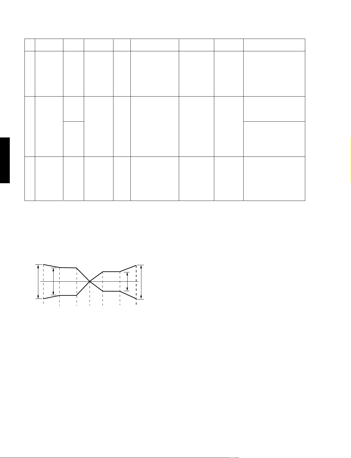
● PLAYBACK FREQUENCY RESPONSE
± 3dB
± 4dB
1k
± 3dB
3k 10kHz31525050 12.5kHz
ACVM
Oscilloscope
± 3.5dB
Fig. C
PLAY
REC OUT
Check that the 10kHz playback
level is within 0 ± 3 dB of the
1kHz playback level. (Fig. C)
22
Page 24
GX-505/GX-505VCD
< Recording section >
Item to be
Step
Adjusted
Recording
1
level
Recording
2
bias
(Total
frequency
response)
Confirmation
3
of recorded
level
GX-505/VCD
Tape
AC-514
High
(CrO2)
AC-514
High
(CrO2)
AC-225
Normal
(LH)
AC-514
High
(CrO2)
Instrument
required
ACVM
Audio
frequency
oscillator
ACVM
Audio
frequency
oscillator
ACVM
Audio
frequency
oscillator
Mode
REC
PLAY
REC
PLAY
REC
PLAY
Measurement
conditions
Input 1 kHz Signal to
AUX IN from Audio
Frequency Oscillator.
Adjust output level of
Audio Frequency Oscillator so that the
voltage of REC OUT
becomes – 27 dBV.
Input 12.5 kHz Signal to AUX IN from
Audio Frequency Oscillator.
Adjust output level of
Audio Frequency Oscillator so that the
voltage of REC OUT
becomes – 27 dBV.
Points of
measurement
REC OUT
REC OUT
REC OUT
Adjustment
parts
VR6 (L ch)
VR5 (R ch)
VR3 (L ch)
VR2 (R ch)
Rating
Adjust for equal record and
playback levels.
(– 27 dBV ± 0.3 dBV)
Adjust for equal record and
playback levels.
(– 27 dBV ± 0.3 dBV)
Adjust for equal record and
playback levels. (Fig. D)
Perform record bias adjustment of High (CrO2) tape
again, if the rating was not
satisfied.
Confirm recorded level rating as in step 1 When recorded level rating is improper, go back to step 1
and also carry out adjustments in step 2 again.
● TOTAL FREQUENCY RESPONSE ( – 27 dBV)
Dolby NR B & OFF
Type I (Normal)/Type II (High)
± 4dB
± 5dB
1k
± 3dB
3k 10kHz31525050 12.5kHz
± 5dB
Fig. D
23
Page 25

0
2
3
4
5
6
7
8
9
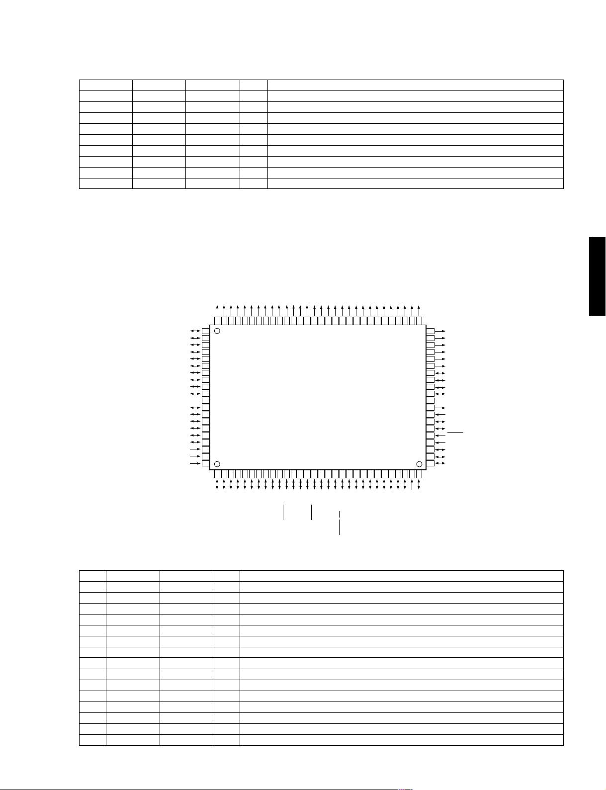
■ IC DATA
IC8 : M38199EF [CD/VCD P.C.B.]
8 bit
µ-COM (CD CPU)
P90/SEG16
P91/SEG17
P92/SEG18
P93/SEG19
P94/SEG20
P95/SEG21
P96/SEG22
P97/SEG23
P30/SEG24
P31/SEG25
P32/SEG26
P33/SEG27
P34/SEG28
P35/SEG29
P36/SEG30
P37/SEG31
P00/SEG32/DIG
P01/SEG33/DIG1
P02/SEG34/DIG
P03/SEG35/DIG
P04/SEG36/DIG
P05/SEG37/DIG
P06/SEG38/DIG
P07/SEG39/DIG
P10/SEG40/DIG
P11/SEG41/DIG
P12/DIG10
P13/DIG11
P14/DIG12
P15/DIG13
GX-505/GX-505VCD
Pin No.
1
2
3
4
5
6
7
8
9
10
11
12
13
14
15
16
17
18
19
20
21
22
23
24
25
26
27
28
29
30
Port
P77
AN6
P75
P74
P73
P72
P71
P70
PB3
PB2
P57
P56
P55
P54
P53
P52
P51
P50
P67
P66
P65
P64
P63
P62
P61
P60
P47
P46
INT1
INT4
P87/SEG15
P86/SEG14
P85/SEG13
P84/SEG12
P83/SEG11
P82/SEG10
P81/SEG9
P80/SEG8
PA7/SEG7
PA6/SEG6
VCC
PA5/SEG5
PA4/SEG4
PA3/SEG3
PA2/SEG2
PA1/SEG1
PA0/SEG0
VEE
AVSS
VREF
8079787776757473727170696867666564636261605958575655545352
81
82
83
84
85
86
87
88
89
90
91
92
93
94
95
96
97
98
99
100
123456789
P77/AN7
P76/AN6
Name
ADR
NTSC
OPSW
/CLSW
/STOP
/UPSW
/DWSW
/FLOCK
P75/AN5
P74/AN4
P73/AN3
I/O
I
I
I
I
I
I
I
I
101112131415161718192021222324252627282930
PB3
PB2/DA
P72/AN2
P71/AN1
P70/AN0
P54/SIN3/AN12
P56/SCLK3/AN14
P57/SRDY3/AN15
P55/SOUT3/AN13
P51/SOUT2/AN9
P52/SCLK2/AN10
P53/SRDY2/AN11
P65/SOUT1
P66/SCLK11
P50/SIN2/AN8
P67/SRDY1/CS/SCLK12
P64/SIN1
Tray table address detect SW
Video out PAL/AUTO/NTSC select detect (GX-505VCD only))
Tray open SW
Tray close SW
Tray table STOP position detect SW
Clamper up SW
Clamper down SW
Focus servo lock
Open
Open
/TLOCK
/SCLK
SOUT
SIN
HSEL
/SCLKD
SOD
SID
/CS
/DCLK
DSO
DSI
STAT
Tracking servo lock
I
Serial clock to servo LSI
O
Serial out to servo LSI
O
Serial in from servo LSI (Q-code or SENSE)
I
O
Address/data select signal (GX-505VCD only))
O
Serial clock from decoder (GX-505VCD only))
O
Serial out to decoder (GX-505VCD only))
I
Serial in from decoder (GX-505VCD only))
System communication chip enable
I
Serial clock from system µ-COM (Auto transfer)
I
Serial out to system µ-COM
O
Serial in from system µ-COM
I
Servo status signal
I
Not used
Not used
Feed origin SW
/FLSW
/HRDY
I
Decoder data out OK signal (GX-505VCD only))
I
Open
BLKCK
Q-code read OK signal
I
Open
P61/PWM
P63/CNTR1
P62/CNTR0
P60
P47/T3OUT
P46/T1OUT
P45/INT1/ZCR
Function
51
50
49
48
47
46
45
44
43
42
41
40
39
38
37
36
35
34
33
32
31
P44/INT4
P16/DIG14
P17/DIG15
P20/DIG16
P21/DIG17
P22/DIG18
P23/DIG19
P24
P25
P26
P27
VSS
X OUT
X IN
PB0/XC OUT
PB1/XC IN
RESET
P40/INT0
P41
P42/INT2
P43/INT3
GX-505/VCD
24
Page 26

GX-505/GX-505VCD
IC8 : M38199EF [CD/VCD P.C.B.]
8 bit
µ-COM (CD CPU)
Pin No.
31
32
33
34
35
36
37
38
39
40
41
42
43
44
45
46
47
48
49
GX-505/VCD
50
51
52
53
54
55
56
57
58
59
60
61
62
63
64
65
66
67
68
69
70
71
72
73
74
75
76
77
78
79
80
81
82
83
84
85
86
87
88
89
90
91
Port
INT3
INT2
P41
INT0
/RESET
XCIN
XCOUT
XIN
XOUT
VSS
P27
P26
P25
P24
P23
P22
P21
P20
P17
P16
P15
P14
P13
P12
P11
P10
P07
P06
P05
P04
P03
P02
P01
P00
P37
P36
P35
P34
P33
P32
P31
P30
P97
P96
P95
P94
P93
P92
P91
P90
P87
P86
P85
P84
P83
P82
P81
P80
PA7
PA6
VCC
25
Name
/HINT
DEPH
/CSINT
RESET
XCIN
XCOUT
XIN
XOUT
GND
K3
K2
K1
K0
KD3
KD2
KD1
KD0
/DECRST
DRV
FCSG
TROP
TRCL
TBL +
TBL –
/MNRST
/MUTE
/PON
DMUTE
/MLD
CMDSEL
QSEL
DOSEL
/TSPD
VMUTE
VCC
I/O
Open
I
Decoder interrupt signal (GX-505VCD only)
O
De-emphasis control (GX-505VCD only)
System µ-COM data automatic transfer initialize, start signal
I
Reset
I
Open
Open
8 MHz (MAIN CLOCK)
I
8 MHz (MAIN CLOCK)
O
GND
Not used
I
Not used
I
Not used
I
Not used
I
Not used
O
Not used
O
Not used
O
Not used
O
Not used
O
Not used
O
Not used
O
Not used
O
Not used
O
O
Decoder reset (GX-505VCD only)
Servo driver on
O
Focus gain high (NC)
O
Tray open control signal (implied clamper control)
O
Tray close control signal
O
Tray table revolution
O
Tray table brake
O
Open
Servo LSI reset signal
O
Open
O
Line mute
O
Servo LSI power ON control
O
Open
O
Digital mute
O
Microprocessor command store request
O
O
Serial 2 ^ µ-COM command
O
Serial 2 ^ Q-code reed
O
Decoder serial I/O out select (GX-505VCD only)
Tray table revolution speed control (H : Low speed)
O
O
Video mute (GX-505VCD only)
Not used
O
Not used
O
Not used
O
Not used
O
Not used
O
Not used
O
Not used
O
Not used
O
Not used
O
Not used
O
Not used
O
Not used
O
Not used
O
Not used
O
Not used
O
Not used
O
Not used
O
+5V
Function
Page 27
IC8 : M38199EF [CD/VCD P.C.B.]
0
2
3
4
5
6
7
8
9
8 bit
µ-COM (CD CPU)
Pin No.
92
93
94
95
96
97
98
99
100
Port
PA5
PA4
PA3
PA2
PA1
PA0
VEE
AVSS
VREF
Name
VEE
AVSS
VREF
I/O
O
O
O
O
O
O
GX-505/GX-505VCD
Function
Not used
Not used
Not used
Not used
Not used
Not used
GND
GND (VSS)
+5V (VCC)
IC8 : M38199EF [INPUT P.C.B.]
8 bit
µ-COM (SYSTEM CPU)
VCC
VEE
AVSS
VREF
81
82
83
84
85
86
87
88
89
90
91
92
93
94
95
96
97
98
99
100
P87/SEG15
P86/SEG14
P85/SEG13
P84/SEG12
P83/SEG11
P82/SEG10
P81/SEG9
P80/SEG8
PA7/SEG7
PA6/SEG6
PA5/SEG5
PA4/SEG4
PA3/SEG3
PA2/SEG2
PA1/SEG1
PA0/SEG0
P90/SEG16
P91/SEG17
P92/SEG18
P93/SEG19
P94/SEG20
P95/SEG21
P96/SEG22
P97/SEG23
P30/SEG24
P31/SEG25
P32/SEG26
P33/SEG27
P34/SEG28
P35/SEG29
P36/SEG30
P37/SEG31
P00/SEG32/DIG
P01/SEG33/DIG1
P02/SEG34/DIG
P03/SEG35/DIG
P04/SEG36/DIG
P05/SEG37/DIG
P06/SEG38/DIG
P07/SEG39/DIG
P10/SEG40/DIG
8079787776757473727170696867666564636261605958575655545352
123456789
P77/AN7
P76/AN6
P75/AN5
P74/AN4
P73/AN3
101112131415161718192021222324252627282930
PB3
PB2/DA
P72/AN2
P71/AN1
P70/AN0
P54/SIN3/AN12
P56/SCLK3/AN14
P57/SRDY3/AN15
P55/SOUT3/AN13
P52/SCLK2/AN10
P53/SRDY2/AN11
P65/SOUT1
P66/SCLK11
P50/SIN2/AN8
P51/SOUT2/AN9
P67/SRDY1/CS/SCLK12
P64/SIN1
P63/CNTR1
P61/PWM
P62/CNTR0
P11/SEG41/DIG
P12/DIG10
P13/DIG11
P14/DIG12
P15/DIG13
51
P60
P44/INT4
P47/T3OUT
P46/T1OUT
P45/INT1/ZCR
50
49
48
47
46
45
44
43
42
41
40
39
38
37
36
35
34
33
32
31
P16/DIG14
P17/DIG15
P20/DIG16
P21/DIG17
P22/DIG18
P23/DIG19
P24
P25
P26
P27
VSS
X OUT
X IN
PB0/XC OUT
PB1/XC IN
RESET
P40/INT0
P41
P42/INT2
P43/INT3
GX-505/VCD
No.
1
2
3
4
5
6
7
8
9
10
11
12
13
14
15
Port
AN7
AN6
AN5
AN4
AN3
AN2
AN1
AN0
PB3
DA
AN15
SCLK3
SO3
SI3
AN11
Name
MSEL
SPEIN
DSEL
KEY4
KEY3
KEY2
KEY1
KEY0
FAN
THER
FLCLK
FLDATA
VPRT
I/O
MODEL/PRO LOGIC MODE DETECT (A-D)
I
SPECTRUM ANALYZER (BA3835F) IN (A-D)
I
MARKET SELECT IN (A-D)
I
KEY 4 IN (A-D)
I
KEY 3 IN (A-D)
I
KEY 2 IN (A-D)
I
KEY 1 IN (A-D)
I
KEY 0 IN (A-D)
I
OPEN
FAN CONTROL OUT
O
AMP THERMAL DETECT
I
SERIAL CLOCK FOR FL DRIVER M66004
O
SERIAL OUT FOR FL DRIVER M66004
O
OPEN
ABNORMAL VOLTAGE DETECT
I
Function
26
Page 28

GX-505/GX-505VCD
IC8 : M38199EF [INPUT P.C.B.]
8 bit
µ-COM (SYSTEM CPU)
No.
16
17
18
19
20
21
22
23
24
25
26
27
28
29
30
31
32
33
34
GX-505/VCD
35
36
37
38
39
40
41
42
43
44
45
46
47
48
49
50
51
52
53
54
55
56
57
58
59
60
61
62
63
64
65
66
67
68
69
70
71
72
73
74
75
Port
SCLK2
SO2
SI2
P67
SCLK1
SO1
SI1
P63
P62
P61
P60
P47
P46
INT1
INT4
INT3
INT2
P41
INT0
/RESET
XCIN
XCOUT
XIN
XOUT
VSS
P27
P26
P25
P24
P23
P22
P21
P20
P17
P16
P15
P14
P13
P12
P11
P10
P07
P06
P05
P04
P03
P02
P01
P00
P37
P36
P35
P34
P33
P32
P31
P30
P97
P96
P95
Name
TUCLK
TUDO
TUDATA
/STAD
SYSCK
SYSO
SYSI
TUMUTE
/AMPMUTE
CDCE
CDRES
MDCE
MDRES
ACIN
PDN
REMO
STEIN
RESET
XCIN
XCOUT
XIN
XOUT
GND
SPEA
SPEB
SPEC
SPESEL
DLCE
KALATCH
FLRES
FLCE
TUCE
STLED
TMLED
/BC
TEST0
TEST1
DSEL0
DSEL1
PRON
SRON
/SMUTE
/A
/YMA
IN1B
IN1A
IN2A
IN2B
RECA
RECB
VSEL0
VSEL1
VCR
PBMUTE
RMUTE
REC
BIAS
DOLBY
I/O
LC72131/LC72720/M65853FP/LA2787/LV1017/LC75393/LC7536Y CLK OUT
O
LC72131/LC72720/M65853FP/LA2787/LV1017/LC75393/LC7536Y DATA OUT
O
LC72131/LC72720 DATA IN
I
STATION IN (TUNER) [L : STATION AVAILABLE]
I
SYSTEM COMMAND CLOCK
O
SYSTEM COMMAND OUT
O
SYSTEM COMMAND IN
I
TUNER MUTE [H : MUTE ON]
O
AMP MUTE [L : MUTE ON]
O
SYSTEM COMMUNICATION CD CE
O
CD RESET
O
SYSTEM COMMUNICATION MD CE
O
MD RESET
O
POWER DOWN AC PULSE IN
I
MD POWER DOWN
O
OPEN
REMOTE CONTROL SIGNAL IN
I
TUNER STEREO/MONO DETECT
I
OPEN
RESET
I
32.768 kHz IN (SUB CLOCK)
I
32.768 kHz OUT (SUB CLOCK)
O
8 MHz IN (MAIN CLOCK)
I
8 MHz OUT (MAIN CLOCK)
O
GND
O
SPECTRUM ANALYZER (BA3835F) A OUT
O
SPECTRUM ANALYZER (BA3835F) B OUT
O
SPECTRUM ANALYZER (BA3835F) C OUT
O
SPECTRUM ANALYZER (BA3835F) SEL OUT
O
LA2787/LV1017 CE
O
KARAOKE IC M65853 LATCH
O
FL DRIVER RESET
O
FL DRIVER CE
O
LC72131/LC72720/LC75393 CE
O
STANDBY LED ON [ H : LED ON ]
O
TIMER LED ON [ H : LED ON ]
O
PRO LOGIC IC CONTROL-BC (Not used)
O
TEST PORT
O
TEST PORT
O
MD DIGITAL INPUT SELECT
O
MD DIGITAL INPUT SELECT
O
POWER RELAY CONTROL [ H : ON ]
O
SPEAKER RELAY CONTROL [ H : ON ]
O
SUB WOOFER MUTE [ L : MUTE ON ]
O
PRO LOGIC IC CONTROL-A [ H : ON ] (Not used)
O
Y MERSION ON [ L : ON ]
O
4052 INPUT SELECT (Note 1)
O
4052 INPUT SELECT (Note 1)
O
4052 INPUT SELECT (Not used)
O
4052 INPUT SELECT (Not used)
O
4066 CONTROL
O
4066 CONTROL
O
LA7956 INPUT SELECT (Not used)
O
LA7956 INPUT SELECT (Not used)
O
VCR REC INHIBIT [ H : INHIBIT]
O
DECK PLAYBACK MUTE
O
DECK REC MUTE
O
DECK AMP REC
O
DECK BIAS ON
O
DOLBY ON
O
Function
27
Page 29

IC8 : M38199EF [INPUT P.C.B.]
8 bit
µ-COM (SYSTEM CPU)
GX-505/GX-505VCD
No.
76
77
78
79
80
81
82
83
84
85
86
87
88
89
90
91
92
93
94
95
96
97
98
99
100
Port
P94
P93
P92
P91
P90
P87
P86
P85
P84
P83
P82
P81
P80
PA7
PA6
VCC
PA5
PA4
PA3
PA2
PA1
PA0
VEE
AVSS
VREF
Name
TPEQ
SOL
CPM
CLOSE
OPEN
ENVA
ENVB
ENMA
ENMB
/HP
MIC
CASS
PLSW
CRO2
/IPRT
+5V
CLSW
RECINHF
RECINHR
OPSW
REEL
MUSIC
VEE
AVSS
VREF
I/O
O
TAPE EQUALIZER SELECT [ H : 120 µ]
O
DECK SOLENOID ON
O
DECK CAPSTAN MOTOR ON
O
TAPE LOADING MOTOR CLOSE
O
TAPE LOADING MOTOR OPEN
I
VR ENCODER A
I
VR ENCODER B
I
MD ENCODER A
I
MD ENCODER B
I
HEAD PHONE DETECT [L : HP DETECT]
I
MIC DETECT
I
CASSETTE IN DETECT
I
DECK MECHA PLAY POSITION DETECT
I
CrO2 (70 µs) POSITION DETECT
I
AMP OVER CURRENT DC VOLTAGE DETECT [L : ABNORMAL DETECT]
+5V
I
DECK CLOSE SW
I
REC INHIBIT FORWARD (SIDE-A)
I
REC INHIBIT REVERSE (SIDE-B)
I
DECK OPEN SW
I
REEL MOTOR PULSE DETECT
I
TAPE MUSIC SENSOR
GND
GND
+5V
Function
GX-505/VCD
(Note 1) Pin 62, 63
IN1B IN1A FUNCTION
(Pin 62) (Pin 63)
0 0 AUX
0 1 TUNER
1 0 TAPE
1 1 CD/VCD
28
Page 30

GX-505/GX-505VCD
IC5 : MN35511AL [CD/VCD P.C.B.]
Signal Processor & Controller
60
VDD
57
VSS
4
DVDD1
5
DVSS1
18
/RST
71
/TEST
32
FE
33
TE
34
RFENV
37
TRCRS
35
VDET
39
BDO
38
/RFDET
36
OFT
GX-505/VCD
A/D CONVERTER
INPUT PORT
SERVO
TIMING GENERATOR
STAT
X1X2XSEL
58 59 5617
TIMING
GENERATOR
PITCH CONTROL
MICRO COMPUTER
OUTPUT
PORT
41
WVEL
SENSE
SMCK/FCLK49VCOF69CK3848MDATA7MCLK9MLD44ARF46DRF45IREF47DSLF48PLLF52EFM53PCK/RESY67AVDD62AVSS15SUBQ14SQCK20CLVS/FLAG668DEMPO73SUBC
19
42
PLAY/TRVSTP
DSL • PLL VCO
CIRC ERROR CORRECTION
INTER POLATION
SOFT MUTING
ATTENUATION
PEAK DETECT
AUTO CUE
29
21
16
26
TRV
KICK
VREF
DMUTE
EFM DEMODULATION
SYNC INTERPOLATION
SUBCODE DEMODULATION
DEINTERLEAVE
DIGITAL
1
BCLK
CLV
SERVO
3
2
23PC24
LRCK
SRDATA
INTERFACE
SERVO
CPU
4010 43
11
TOFS
LDON
/FLOCK12/TLOCK
VCO
D/A
CONVERTER
30
28
27
TRD
FOD
FBAL31TBAL
22
25
TVD
ECS
SUBCODE
BUFFER
ECM
16k
SRAM
DIGITAL
AUDIO
INTERFACE
6TX76
72
SBCK2
74
54
IPFLAG
SBCK75CLDCK13BLKCK55CRC
FLAG
SDATI80BCKI79LRCKI77DEMPI/TEST2
IOSEL
78
70
DIGITAL DE-EMPHASIS
8 TIMES
OVER SAMPLING
DIGITAL FILTER
DD type
DAC
PEM
(L)
51
63
64
AVSS2
OUT1C
OUT1D66OUT2C
PLL
VCO 2
PEM
(R)
65
50
AVDD2
OUT2D
61
VCOF2
Pin No.
1
2
3
4
5
6
7
8
9
10
11
12
13
14
15
16
17
18
19
20
21
22
23
24
25
26
27
28
29
30
31
32
Name
BCLK
LRCK
SRDATA
DVDD1
DVSS1
TX
MCLK
MDATA
MLD
SENSE
FLOCK
TLOCK
BLKCK
SQCK
SUBQ
DMUTE
STAT
RST
SMCK/
FCLK
CLVS/
FLAG6
TRV
TVD
PC
ECM
ECS
KICK
TRD
FOD
VREF
FBAL
TBAL
FE
I/O
Bit clock output for SR DATA
O
L/R identification signal output
O
Serial data output
O
Power supply for digital circuit (+5)
I
GND for digital circuit
I
Digital audio interface output signal
O
Microprocessor command clock signal input (data latched at leading edge)
I
Microprocessor command data input
I
Microprocessor command load signal input (L : LOAD)
I
Sense signal output (OFT, FESL, NACEND, NAJEND, SFG, NWTEND)
O
Focus servo drawing signal (L : when drawn)
O
Tracking servo drawing signal (L : when drawn)
O
Sub code block clock signal (BLKCK=75Hz)
O
Clock input for sub-code Q register
I
Sub-code Q code output
O
Muting input (H : MUTE)
I
Status signal (CRC, STCNT, CLVS, TTSTOP, SQOK, RESY, FCLV, FLAG6, SENSE ,/FLOCK, /RFDET, /TLOCK)
O
Reset input (L : RESET)
I
4.2336MHz clock signal output SMCK when command is defaulted. (Note 1) (NC)
O
Function
SMCK (8.4672MHz), FCLK (7.35kHz) or “L” fixed is selected when command is switched.
With command defaulted : CLVS when IOSEL=H, FLAG6 when IOSEL=L (NC)
O
These settings can be reversed by command (FLAG6 when IOSEL=H).
Traverse (Feed) forced feed output 3-State
O
Traverse (Feed) drive output
O
Spindle motor ON signal L : ON (default) (NC)
O
Spindle motor drive signal (forced mode output) 3-State
O
Spindle motor drive signal (servo error signal output)
O
Kick pulse output 3-State
O
Tracking drive output
O
Focus drive output
O
Reference voltage for DA output block (TVD, ECS, TRD, FOD, FBAL, TBAL)
I
Focus balance adjustment output
O
Tracking balance adjustment output
O
Focus error signal input (analog input)
I
(Note 1) At the SMCK/FCLK pin, output does not stop while /RST=L.
29
Page 31

IC5 : MN35511AL [CD/VCD P.C.B.]
Signal Processor & Controller
GX-505/GX-505VCD
Pin No.
33
34
35
36
37
38
39
40
41
42
43
44
45
46
47
48
49
50
51
52
53
54
55
56
57
58
59
60
61
62
63
64
65
66
67
68
69
70
71
72
73
74
75
76
77
78
79
80
TE
X1
X2
I/O
I
I
I
I
I
I
I
O
O
O
O
I
I
I
I/O
I/O
I/O
I
I
O
O
O
O
I
I
I
O
I
O
O
O
O
O
O
I
O
O
I
I
I
O
I
O
O
I
I
I
I
Name
RFENV
VDET
OFT
TRCRS
RFDET
BDO
LDON
TOFS
PLAY/TRVSTOP
WVEL
ARF
IREF
DRF
DSLF
PLLF
VCOF
AVDD2
AVSS2
EFM
PCK/
RESY
FLAG
CRC
XSEL
VSS
VDD
VCOF2
AVSS1
OUT1C
OUT1D
OUT2D
OUT2C
AVDD1
DEMPO
CK384
IOSEL
TEST
SBCK2
SUBC
SBCK
CLDCK
IPFLAG
DEMPI
/TEST2
SDATI
LRCKI
BCKI
Function
Tracking error signal input (analog input)
RF envelope signal input (analog input)
Oscillation detect signal input (H : DETECT)
Off track signal input (H : OFF TRACK)
Track cross signal input (analog input)
RF detect signal input (L : DETECT)
Drop out signal input (H : DROP OUT)
Laser ON signal output (H : ON)
Tracking offset adjustment output (NC)
Switched by command. PLAY (Play signal output) when command is defaulted. (NC)
Double speed status signal output (H : double speed) (NC)
RF signal input
Reference current input terminal
Bias terminal for DSL
Loop filter terminal for DSL
Loop filter terminal for PLL
Loop filter terminal for VCO (NC)
Power supply for analog circuit (for AD of DSL, PLL, DA output blocks) (+5)
GND for analog circuit (for AD of DSL, PLL, DA output blocks) (GND)
EFM signal output (NC)
With command defaulted : PLL extract clock output PCK when IOSEL=H, frame re-synchronous signal RESY when IOSEL=L
These settings can be reversed by command (RESY when IOSEL=H). (NC)
Flag signal output (NC)
Sub-code CRC check result output (H : OK, L : NG) (NC)
L : Normal mode (GND)
H : • For internal master clock, VCO2 output clock for jitter adsorbing PLL is used instead of Xtal
oscillation output (X2).
• VCO2 is always fixed to oscillation mode regardless of VCO2 oscillation stop command or
resetting (/RST=L) and Xtal oscillation is stopped.
GND for oscillation circuit
Crystal oscillation circuit input terminal
Crystal oscillation circuit output terminal
Power supply for oscillation circuit (+5)
PLL loop filter terminal for jitter adsorption (GND)
GND for audio DAC
PEM output terminal 1C
PEM output terminal 1D
PEM output terminal 2D
PEM output terminal 2C
Power supply terminal for audio DAC
Deemphasis detect signal output (NC)
384fs clock output (At the CK384 pin, output does not stop while /RST=L.) (NC)
Xtal system when command is defaulted. Signal processing system when command is switched
Mode selecting terminal (GX-505 : +5, GX-505VCD : GND)
Test mode setting terminal (Normal : H) (+5)
Sub-code data read clock input (NC)
Sub-code serial output (SBCK effective) when command is defaulted.
PACK data usable (SBCK2 effective) when command is switched
Clock input for sub-code serial output (with pull-up resistor) (GX-505 : NC)
Sub-code frame clock signal output when command is defaulted (fCLDCK=7.35kHz)
PACK synchronous signal when command is switched
Interpolation flag signal output (H : INTERPOLATION) (GX-505 : NC)
When IOSEL=H, L : NORMAL H : TEST2 (GND)
Emphasis control in accordance with DEMP0
When IOSEL=L, external DEMP1 input terminal
For emphasis control, DEMP0, OR of DEMP1, DEMP1, forced OFF or forced ON is selected by command.
When command is defaulted, DEMP0 and OR of DEMP1
SRDATA input (effective only when IOSEL=L)
LRCK input (effective only when IOSEL=L) H : Lch data, L : Rch data
BCK input (effective only when IOSEL=L)
GX-505/VCD
30
Page 32

GX-505/GX-505VCD
■ DISPLAY DATA
● V800 : 16-BT-63GK (V2959000)
q%9
PATTERN AREA
● PIN CONNECTION
Pin No. 123456789101112131415161718192021222324252627282930
Connection F1 F1 NP NP P35 P34 P33 P32 P31 P30 P29 P28 P27 P26 P25 P24 P23 P22 P21 P20 P19 P18 P17 P16 P15 P14 P13 P12 P11 P10
Pin No. 31 32 33 34 35 36 37 38 39 40 41 42 43 44 45 46 47 48 49 50 51 52 53 54 55 56 57 58 59
Connection P9 P8 P7 P6 P5 P4 P3 P2 P1 16G 15G 14G 13G 12G 11G 10G 9G 8G 7G 6G 5G 4G 3G 2G 1G NP NP F2 F2
Note 1) F1, F2 ......... Filament
2) NP .............. No Pin
3) NC .............. No Connection
4) P1~P35....... Datum Line
5) 1G~16G...... Grid
GX-505/VCD
● GRID ASSIGNMENT
31
Page 33

● ANODE CONNECTION
GX-505/GX-505VCD
(RIGHT)
(LEFT)
(LEFT)
(RIGHT)
(BELOW)
(UPPER)
(RIGHT)
(CENTER)
(LEFT)
GX-505/VCD
32
Page 34

GX-505/GX-505VCD
PK1
AM
COIL PACK
IF AMP
Q1
CERAMIC
FILTER
L1
CERAMIC
FILTER
L2
8
1
27
L.P.F
L.P.F
TUNER.R
TUNER.L
TUNER
AM/FM IF
MPX
IC1
LA1838
PLL
IC2
LC72131M
PK2
AM STEREO
IC3
TA2040AF
RDS
IC4
LC72720NM
XL3
10.7MHz
XL1
1FM IN
9
16
17
18
19
22
6 7 13 15
20 ~ 23
2
12 13
4.332MHz
XL4
RDS
(B,G only)
+5.0
AM
STEREO
(J only)
7
9
4
5
30
AM IN
AM OSC
FM OSC
FM VT
43
FM
ANT
GND
AM
ANT
AM VT 18
1 20181413
2
~
5
9
11
L5
L6
TUNER CONTROL
XL2
(TUNER) Page 69
■ BLOCK DIAGRAM
GX-505/VCD
33
Page 35

ABCDEFGH
GX-505/GX-505VCD
■ BLOCK DIAGRAM
1
(CD/VCD) Page 62, 63
+D5
CD
TRAVERSE UNIT
A
B
C
D
E
F
2
LASER
FOCUS
3
4
TRACKING
M
M
LIMIT SW
SPINDLE
FEED
LD
GND
PD
VR
FCS
TRK
+5
Q2
LD
DRIVE
35
36
33
34
6
7
12
13
24
25
30
31
HEAD
AMP
IC4
AN8806SB
2
1
+D5
ACT
MOTOR
DRIVE
IC1
M56748FP
5
TP1
10
3
27
13
29
|
30
17
19
|
25
XL1
16.9344MHz
4
15
21
22
33
17
18
20
+5.4V
26
1,9 1,9
MOTOR
DRIVE
IC2
73
44
30
|
41
58
59
4, 50, 60, 71
SERVO SIGNAL
PROCESSOR
MN35511AL
21,22,24-28
MOTOR
DRIVE
IC3
3
DF.DAC
IC5
7,10,14,15
BUS
BUFFER
IC9
26
7
6
XL2
8MHz
U+5
+B
63
64
65
66
1
|
3
8
9
11
12
+12V
73
|
76
78
|
80
16
|
18
38
39
30
|
41
69
70
26
IC13, 14
4, 8
62,67,68
8,11,13,23,
59,60
57,58
±12V
32-34
15,27,29,
CD CPU
IC8
1,3-7
MUTE
Q11, 12
64
65
73
16
17
18
71
54
19
|
22
35
Q10 Q6, 7
+5.4V
ON/OFF
+D5
+3.3
(INPUT) Page 64, 65
D.OUT
CD
MUTE
VCD
MODULE
IC11
Q9
IC6
BUS
BUFFER
IC10
IC10
IC7, Q8
(VCD only)
CB402 (GX-505VCD)
CB420 (GX-505)
Q403,404
CD CONTROL
VIDEO
OUT
(VCD only)
CDB (FROM MAIN)
CASSETTE MECHA
R/P HEAD
E HEAD
LOAD
LOAD OUT
LOAD IN
R,REC
F,REC
CASS
CrO
SOL
SENSOR
OUT
+5V
M
2
(INPUT) Page 64, 65
K9V
DECK
1
+
-
9,1 7,3
R/P
SWITCH
IC2
E+
E-
IC8 73 REC
IC8 95 OPSW
5.0V
IC8 92 CLSW
IC8 94 RECINHR
IC8 93 RECINHF
IC8 87 CASS
IC8 89 CrO
Q1
5.0V
IC8 88 PLSWPLAY
BIAS
VR2,3
PB LEVEL
VR1,4
2
10
2
IC8 96 REEL
BIAS
TRAP
L2,3
L1,Q12
MOTOR
DRIVE
IC1
BIAS
OSC.
41
44
48
37
9
26
DRIVE
5
6
SOL
Q3,4
DOLBY
R/P AMP
IC6
Q8 Q10 Q9
BIAS
POWER
Q13,14,17,
18,34
IC8 80 OPEN
IC8 79 CLOSE
IC8 77 SOL
32
5
REC LEVEL
13
24
14
VR5,6
23
11
26
29
3
1718,19 104
27
Q16
IC8 72 RMUTE
IC8 97 MUSIC
IC8 73 REC
IC8 76 TPEQ
IC8 75 DOLBY
IC8 71 PBMUTE
+B
IC8 74 BIAS
IC8 76 TPEQ
TAPE REC
Q35,36
IC8 76 TPEQ
TAPE PB
PAL
5
AUTO
NTSC
(VCD only)
SW1
IC8 2
M
SLIDE
TRAY
MOTOR
M
ROTAR Y
MOTOR
TABLE
POSITION
DETECT
OP/CLSWUP/DWN
SW
TRAY
POSITION
DETECT
M
MTR
MTR
SPEEDB
SPEEDA
TAPE SPEED
VR7
MOTOR
DRIVE
Q2,11
IC8 78 CPM
CD MECHA UNIT
34 35
6
Page 36

ABCDEFGH
GX-505/GX-505VCD
■ BLOCK DIAGRAM
1
(INPUT) Page 64, 65
12
IN
AUX/MD
OUT
2
TUNER
TAPE PB
CD
TAPE REC
AUX
TUNER
TAPE
1
14
5
INPUT
SWITCH
15
2
11
CD
4
4
SWITCH
9
5,6
IC3
REC
IC5
12,13
13
3
3
8
Q5,7
Q6,15
RECB
RECA
Q29,309,10
IC8 67
IC8 66
IC21
3
1
5
7
HP AMP
IC10
5
3
7
1
INIA
INIB
IC8
62,63
(GX-505 only)
35
17
IC9
49
64
14
35
11
12
23 24 19
VOLUME LEVEL
CONTROL
GEQ
IC7
24 25 26
YMERSION
TONE.CONT.
IC804
21
28
15
34
TUCE,TUDO,TUCLK
22
18
13
20
IC8 49,17,16
4
6
MUTE
Q23.24
IC807
2
8
IC11
13
IC8 59
MUTE
Q201
Q202
AMPMUTE
IC8 24
SMUTE
MUTE
Q21
(OPE) Page 66, 67
MUTE
Q801
Q802
POWER AMP
IC201
18
22
17
IC8 11
THER
IC8 90
IPRT
±HB
±LB
PROTECTION
SUBWOOFER
OUT
5.0V
HP,IC8 85
HP JACK
JK802
14
15
RY201
TE201
+
+
-
SPEAKER
(MAIN) Page 68
(INPUT) Page 64, 65
3
4
9
(VCD only)
MIC MIXING
D.ECHO
IC800
8
40,41,427,12
MIC VOLUME
VR800
31
32
36
35
DATA
CLOCK
LATCH
MIC SW
IC806
4
6
2
8
IC805
4
2
6
8
32.768MHz
8MHz
XL401
XL402
INIA
62 6663 67
D,SEL
SW2
(R,T)
INIB
3
RESET
8
SPEANA
IC26
17
10
|
13
38 39 3736
16
17
46
86
41
|
44
2
20
|
22
25
26
16-19, 23, 33, 49
U800
REMOCON
32
(OPE) Page 67
MIC1
JK800
4
5
MIC2
JK801
CD CONTROL
TUNER CONTROL
BASS
VR804
(OPE) Page 66, 67
DECK CONTROL
RECB
RECA
71 - 80,87 - 89,92 - 97
SYSTEM CPU
IC8
91
50
35
VCC
81,82
ROTAR Y
ENCODE
SW828
TREBLE
VR802
CONT
61
16 17 49
4 - 8
VOL.
KEY CONT
SW800-827,829-831
SW826
VCD only
(OPE) Page 66, 67
D21
+12M
12V
-12V
-27V
9.0V
K9V
RESET
U5.6V
5.0V
THER
VPRT
11
15
SMUTE
59
AMP
MUTE
24
IPRT
90
SPON
58
PRON
57
HPIN
85
ACIN
29
48
47
12
13
13
|
16
2
3
4
VCC
K9V
5.0V
9.0V
DRIVER
DRIVER
IC802
FL
IC803
32
VP
-27V
LED
u5.6V
Q19
Q33
K9V
Q26
9.0V
+12M
12V
12
14
64
16
D11
C103
-27V
Q204Q25
12V
Q218
+12M
1
|
|
5
|
SUB
+5V
FL DISPLAY
D803
V800
Q206
-27V5.0V
D804
Q27
u5.6V
+HB
-HB
+LB
-LB
-12V
SPON
IC8 58
D211
D212
Q207
-12V
1
2
58
59
D800 — 802, 805 — 833
FAC1
FAC2
(TO CD)
CDB
RY201
IC8 57
IC8 15
VPRT
D213
PRON
F201
SUBB
+12V
D215
RY203
T202
F217
RY203
T203
D22
IC8 29
ACIN
36 37
6
Page 37

ABCDEFGH
GX-505/GX-505VCD
■ PRINTED CIRCUIT BOARD (Foil side)
1
CIRCUIT CHANGES BY MARKET.
TUNER P.C.B.
(Lead Type Device)
TUNER P.C.B.
(Surface Mount Device)
X3 X X O
X4 X O X
IC3 X X O
IC4 X O X
916
81
Q4 X X O
D6 ~ 8, 10 X X O
L7 ~ 9 X O X
C68, 71 ~ 74 X O X
C46, 52 ~ 54 X X O
TUL
2
E
TUR
12V
TUMUTE
TUCE
TUDATA
TUCLK
TUDO
STAD
STEIN
1
12
13 24
u
C29 O O X
C42 ~ 51, 55, 56 X X O
C67, 69, 70 X O X
R33 ~ 38 X X O
R54 X O X
R25 O O X
R39 X X O
J21 X O X
J1, 40, 44 X X O
O : USED
X : NOT USED
U, C, R, T, L, A B, G J
110
3
1630
1630
11 20
y
Point y (Pin20 of IC2)
V : 2V/div H : 0.1 µsec/div
DC range 1 : 1 p robe
115
FROM: INPUT(1)
115
0V
4
W1
Point u (Pin12 of IC4)
V : 2V/div H : 0.1 µsec/div
DC range 1 : 1 p robe
AM GND FM
0V
5
● Semiconductor Location
Ref. No. Location
D1 D2
D2 D2
D3 D2
D4 D2
D5 E3
D6 D2
D7 D2
D8 D2
D9 D2
D10 D2
D11 E4
Ref. No. Location
IC1 A3
IC2 E3
IC3 D2
IC4 E2
Ref. No. Location
Q1 B4
Q2 B4
Q3 B3
Q4 B2
38 39
6
Page 38

ABCDEFGH
118
3619
1
30
80
51
31
50
100
81
120
60 41
21
40
80
61
118
3619
14
85
14
85
1
17
148
7
148
GX-505 CD P.C.B.
(Surface Mount Device)
1 2
GX-505/GX-505VCD
■ PRINTED CIRCUIT BOARD (Foil side)
1
2
LED (CA)
POS SW
COLLE
OPEN SW
TUDN SW
LOADMTR (–)
TUUP SW
FROM : CD MECHA.
GX-505 CD P.C.B.
(Lead Type Device)
LED (AN)
ROTMTR (+)
ROTMTR (–)
CLOSE SW
GND
LOADMTR (+)
● Semiconductor Location
Ref. No. Location
FROM : CD MECHA.
LMSW
LMSW
FMMTR (–)
FMMTR (+)
SPMTR (–)
SPMTR (+)
9
9
1
1
D1 F2
D2 E2
D4 E4
D5 E4
D6 E4
D7 E4
Ref. No. Location
IC1 F2
IC2 B3
IC3 B3
IC4 E4
IC5 F3
IC7 B4
IC8 F3
IC9 F4
IC10 F4
IC13 G4
IC14 G4
Ref. No. Location
Q1 C1
Q2 B3
Q3 C1
Q4 B3
Q5 C4
Q6 B4
Q7 B4
Q8 B5
Q9 B4
Q10 B5
Q11 C5
Q12 C5
Q13 C4
3
VCC
TR (+)
FO (–)
LD
PD
1/2VCC
E
D
A
B
C
F
LDGND
VR
FO (+)
TR (–)
4
FROM : PICK UP HEAD
5
FROM : INPUT (3)
TX
GND
+5
GND
GND
+B
FROM : MAIN (1)
–12V
A GND
D GND
DSO
/CDRES
/DCLK
A GND
FROM : INPUT (1)
L
R
12V
/CS
DSI
µ5.6V
VSEL
A GND
Point q (Pin59 of IC5)
V : 2V/div H : 50 nsec/div
DC range 1 : 1 probe
Point w (Pin39 of IC8)
V : 2V/div H : 0.1 µsec/div
DC range 1 : 1 probe
40 41
6
0V
0V
Page 39

ABCDEFGH
GX-505/GX-505VCD
■ PRINTED CIRCUIT BOARD (Foil side)
1
GX-505VCD VCD P.C.B.
(Lead Type Device)
LMSW
LMSW
FMMTR (–)
FMMTR (+)
SPMTR (–)
SPMTR (+)
FROM : CD MECHA.
GX-505VCD VCD P.C.B.
(Surface Mount Device)
● Semiconductor Location
Ref. No. Location
D1 F2
D2 E2
D4 E4
D5 E4
D6 E4
D7 E4
118
3619
1 2
2
FROM : CD MECHA.
100
130
81
31
50
80
51
LED (CA)
POS SW
COLLE
OPEN SW
TUDN SW
LOADMTR (–)
TUUP SW
LED (AN)
ROTMTR (+)
ROTMTR (–)
CLOSE SW
GND
LOADMTR (+)
9
9
1
1
FROM : VCD MODULE
3
VCC
TR (+)
FO (–)
LD
PD
1/2VCC
E
D
A
B
C
F
LDGND
VR
FO (+)
TR (–)
CLDCK
HSEL
CDLACK
CDSCK
HCK
SBCK
DI DATA
HARDY
EMPH
DGND
D+3.3V
R+5V
VGND
COUT
A+3.3V
BLKCK
SUBC
IPFLG
CDDATA
HDIO
VRST
HINT
DISCK
DILRCK
XCK
DGND
D+3.3V
VGND
YOUT
CVOUT
40
60 41
118
3619
61
21
20
1
80
1
8
17
814
169
17
1
148
148
7
Ref. No. Location
IC1 F2
IC2 B3
IC3 B3
IC4 E4
IC5 F3
IC6 B4
IC7 B4
IC8 F3
IC9 F4
IC10 F4
IC11 F3
IC12 F3
IC13 G4
IC14 G4
Ref. No. Location
Q1 C1
Q2 B3
Q3 C1
Q4 B3
Q5 C4
Q6 B4
Q7 B4
Q8 B5
Q9 B4
Q10 B5
Q11 C5
Q12 C5
Q13 C4
4
14
FROM : PICK UP HEAD
–12V
A GND
D GND
DSO
/CDRES
/DCLK
5
TX
GND+5NC
FROM : INPUT (2)
VIDEO
GND
V MUTE
GND
GND
+B
L
12V
FROM : MAIN (1)
A GND
FROM : INPUT (1)
R
/CS
DSI
µ5.6V
VSEL
A GND
Point q (Pin59 of IC5)
V : 2V/div H : 50 nsec/div
DC range 1 : 1 probe
0V
Point w (Pin39 of IC8)
V : 2V/div H : 0.1 µsec/div
DC range 1 : 1 probe
0V
85
85
14
42 43
6
Page 40

ABCDEFGH
GX-505/GX-505VCD
■ PRINTED CIRCUIT BOARD (Foil side)
1
GX-505 INPUT P.C.B. (3)
GX-505 INPUT P.C.B. (1) (Lead Type Device)
(Lead Type Device)
HP.GND
5V
HPIN
HP.GND
MUTESW
YMA
E
E
E
E
+12V
MDJA
DGND
W17
HP.R
HP.L
E
TONE.RIN
TONE.LIN
E
TONE.ROUT
TONR.LOUT
AGND
-12V
U5.6V
12V
DGND
AGND
AGND
VSEL
SYSCK
SYSO
CDRES
CDCE
SYSI
FROM : CD
DGND
U5.6V
-12V
12V
R
E
L
TUR
TUL
E
W6
W5
TUMUTE
12V
TUCE
TUDO
TUDATA
TUCLK
W6
FROM : TUNER
STEIN
STAD
FREQUENCY
STEP
(R only)
HP.GND
HP.R
HP.L
E
TONE.RIN
TONE.LIN
E
TONE.ROUT
TONR.LOUT
SUBWOOFER
OUT
FROM : OPERATION(2)
REC LEVEL ADJ.
5.0V
GND
DOUT
W420
2
TO : CD
DIGITAL OUT
#30
W3
GX-505 INPUT P.C.B. (3)
(Surface Mount Device)
3
TO : DECK
#29
W4
TO : DECK
#31
W2
TO : DECK
TAPE SPEED ADJ.
PLAY-SW
5V-SEBSOR
SENSOR-OUT
PB LEVEL ADJ.
DGND
+MCR
+SOL
CRO2
PACK
F.REC
R.REC
Rch+
Lch+
AGND
RchLch-
CLOSE.SW
OPEN SW
CLOSE
OPEN
MA
MB
NC
E+
E-
1
10
(Lch)
(Rch)
91
(Lch)
(Rch)
(Lch)
(Rch)
5V
HP.R
HP.L
-
TUNE.RIN
TONE.LIN
TONE.ROUT
TONE.LOUT
-12V
5V
MDJB
DGND
U5.6V
BIAS ADJ.
FROM : OPERATION(2)
4
● Semiconductor Location
Ref. No. Location
IC1 C2
IC2 D3
IC10 G4
IC26 F4
5
Ref. No. Location
Q2 C3
Q3 C3
Q4 C4
Q11 C3
Q12 D3
Q13 D3
Q17 D3
Q25 G4
Q26 G4
Q27 E4
Q28 F4
Q33 E4
TO : OPERATION(2)
#22
DGND
REM
SUB+5V
VREF
KEY1-1
KEY0
VOL A IN
VOL B IN
STANBY
TIMER
5.0V
FLRES
FLCE
FLCLK
FLDAT
FLGND
VP
FL1
FL2
DGND
W12
TO : MAIN(1)
#17
DGND
KEY4
KEY3
W16
KEY2
KEY1
KEY1-1
-27V
26V
+12M
KGND
-LB
TO : MAIN(1)
10 18
91
12V
AGND
-12V
FAC1
FAC2
12V
-12V
#15
W14
MUTE
UGND
THER
18
PREOC
AGND
PREOL
DGND
PREOR
IPRT
SRON
VPRT
-LB
KGND
FAN
SUBE
PRON
SUBB
ACIN
#16
W15
TO : MAIN(2)
OUT
AUX/MD
IN
44 45
6
Page 41

ABCDEFGH
GX-505/GX-505VCD
■ PRINTED CIRCUIT BOARD (Foil side)
1
Point e (Pin37 of IC8)
V : 2V/div H : 20 µsec/div
DC range 1 : 1 probe
GX-505 INPUT P.C.B. (1) (Surface Mount Device)
0V
Point r (Pin39 of IC8)
V : 2V/div H : 50 µsec/div
2
DC range 1 : 1 probe
0V
Point t
6
3
7
3
4
5
2
2
3
1
2
11
8
4
CH1 : Collector of Q19
CH2 : Anode of D11
3
V : 2V/div (CH1) V : 2V/div (CH2)
B, G only
65
1
C
H : 2 sec/div DC range 1 : 1 probe
(This waveform is not available by pushing the power
switch ON and OFF.)
CH 1
CH 2
With the POWER ON,
disconnect the A/C
power cord. Reconnect
the A/C power cord and
4
the above waveforms will
start.
Disconnect the power
cord from the AC
outlet.
t
8
8
0
1
1
0
0
1
5
1
5
0
3
3
1
0
85
14
81
916
85
14
4
6
1
6
1
7
1
3
9
4
8
4
3
2
3
71
814
14
85
● Semiconductor Location
Ref. No. Location
D3 C2
D4 C3
D5 C3
D6 E4
D7 F2
D8 D3
D10 E4
5
D11 D3
D12 D4
D20 G4
D21 F4
D22 F4
D23 F4
D24 E4
D25 E4
D26 E4
Ref. No. Location
IC3 G2
IC5 G2
IC6 C3
IC7 F3
IC8 E3
IC9 G3
IC11 G4
IC21 F2
Ref. No. Location
Q1 C2
Q5 G2
Q6 F2
Q7 G2
Q8 D3
Q9 D3
Q10 D3
Q14 D4
Q15 F2
Q16 C3
Q18 D3
Q19 D3
Q20 G4
Q21 G4
Q22 F4
Q23 F4
Q24 F4
Q29 F2
Q30 F2
Q34 D4
Q35 D2
Q36 D2
er
46 47
6
Page 42

ABCDEFGH
GX-505/GX-505VCD
■ PRINTED CIRCUIT BOARD (Foil side)
1
GX-505VCD INPUT P.C.B. (2)
GX-505VCD INPUT P.C.B. (1) (Lead Type Device)
DSEL1
N.C
N.C
TO : VCD(1)
+12V
N.C
#40
W403
TO : VCD(1)
#39
W401
#31
W2
TO : DECK
FROM : OPERATION(2)
FROM : OPERATION(3)
REC LEVEL ADJ.
1
10
5V
HP.R
HP.L
-
TUNE.RIN
TONE.LIN
TONE.ROUT
TONE.LOUT
-12V
5V
MDJB
5V
HPIN
HP.GND
MUTESW
YMA
E
E
E
E
+12V
MDJA
DGND
HP.GND
HP.R
HP.L
E
TONE.RIN
TONE.LIN
E
TONE.ROUT
TONR.LOUT
AGND
AGND
VSEL
FROM : VCD
CDRES
SYSCK
DGND
CDCE
U5.6V
SYSO
SYSI
R
FROM : TUNER
#34
W1
-12V
12V
E
L
TUMUTE
TUDATA
TUCLK
STEIN
TUDO
TUCE
TUR
TUL
E
STAD
12V
TO : INPUT(2)
Lead Type Device
DSEL0
FROM : INPUT(1)
2
GND
5V
FREQUENCY
DGND
-12V
AGND
12V
U5.6V
U5.6V
DGND
KEY3
KEY4
DGND
#17
W16
TO : MAIN(1)
KEY2
W6
KEY1
KEY1-1
5.0V
DGND
DSEL0
DSEL1
VSEL0
VSEL1
/ VCR
12V
HP.GND
HP.R
HP.L
E
TONE.RIN
TONE.LIN
E
W6
TONE.ROUT
TONR.LOUT
W5
10 18
91
12V
AGND
-12V
FAC1
FAC2
12V
-12V
-27V
26V
+12M
KGND
-LB
MUTE
UGND
THER
AGND
PREOL
DGND
PREOR
IPRT
SRON
VPRT
18
PREOC
-LB
KGND
FAN
SUBE
PRON
SUBB
ACIN
#16
W15
TO : MAIN(2)
#15
W14
TAPE SPEED ADJ.
DGND
+MCR
PLAY-SW
5V-SEBSOR
SENSOR-OUT
+SOL
CRO2
PACK
F.REC
R.REC
PB LEVEL ADJ.
Rch+
Lch+
AGND
CLOSE.SW
OPEN SW
CLOSE
MA
MB
NC
E+
E-
RchLch-
OPEN
(Lch)
(Rch)
91
TO : DECK
-
GND
VMUTE
GND-VIDEO
MONITOR
3
OUT
DOUT
DIGITAL
OUT
#30
W3
TO : DECK
#29
W4
GX-505VCD INPUT P.C.B. (2)
(Surface Mount Device)
BIAS ADJ.
FROM : OPERATION(2)
4
TO : OPERATION(3)
● Semiconductor Location
Ref. No. Location
5
IC1 C2
IC2 D3
IC10 G4
IC26 F4
Ref. No. Location
Q2 C3
Q3 C3
Q4 C4
Q11 C3
Q12 D3
Q13 D3
Q17 D3
Q25 G4
Q26 G4
Q27 E4
Q28 F4
Q33 E4
Q402 A4
Q403 A2
Q404 A2
(Lch)
(Rch)
(Lch)
(Rch)
#22
E
LIN
E
RIN
E
MIC.ROUT
E
MIC.LOUT
E
-
W17
MICSW
LACTH
CLOCK
DATA
DGND
REM
SUB+5V
VREF
KEY1-1
KEY0
VOL A IN
VOL B IN
STANBY
TIMER
5.0V
FLRES
FLCE
FLCLK
FLDAT
FLGND
VP
FL1
FL2
DGND
W12
TO : MAIN(1)
STEP
(R,T only)
TV MODE
SUBWOOFER
OUT
OUT
AUX/MD
IN
48 49
6
Page 43

ABCDEFGH
GX-505/GX-505VCD
■ PRINTED CIRCUIT BOARD (Foil side)
1
Point e (Pin37 of IC8)
V : 2V/div H : 20 µsec/div
DC range 1 : 1 probe
GX-505VCD INPUT P.C.B. (1) (Surface Mount Device)
0V
Point r (Pin39 of IC8)
V : 2V/div H : 50 µsec/div
2
DC range 1 : 1 probe
0V
Point t
36 25
37 24
48 13
112
CH1 : Collector of Q19
CH2 : Anode of D11
3
V : 2V/div (CH1) V : 2V/div (CH2)
H : 2 sec/div DC range 1 : 1 probe
(This waveform is not available by pushing the power
switch ON and OFF.)
CH 1
CH 2
With the POWER ON,
disconnect the A/C
power cord. Reconnect
the A/C power cord and
4
the above waveforms will
start.
Disconnect the power
cord from the AC
outlet.
t
80
81
100
1
51
50
30
31
85
14
81
916
85
14
64
1
16
17
32
49
33 48
71
814
14
85
● Semiconductor Location
Ref. No. Location
D3 C2
D4 C3
D5 C3
D6 E4
D7 F2
D8 D3
D10 E4
5
D11 D3
D12 D4
D20 G4
D21 F4
D22 F4
D23 F4
D24 E4
D25 E4
D26 E4
Ref. No. Location
IC3 G2
IC5 G2
IC6 C3
IC7 F3
IC8 E3
IC9 G3
IC11 G4
IC21 F2
Ref. No. Location
Q1 C2
Q5 G2
Q6 F2
Q7 G2
Q8 D3
Q9 D3
Q10 D3
Q14 D4
Q15 F2
Q16 C3
Q18 D3
Q19 D3
Q20 G4
Q21 G4
Q22 F4
Q23 F4
Q24 F4
Q29 F2
Q30 F2
Q34 D4
Q35 D2
Q36 D2
er
50 51
6
Page 44

ABCDEFGH
GX-505/GX-505VCD
■ PRINTED CIRCUIT BOARD (Foil side)
1
OPERATION P.C.B. ( 2 )
(Lead Type Device)
BASS
GX–505VCD only
TO : OPERATION (3)
TO : OPERATION (4)
2
● Semiconductor Location
Ref. No. Location
IC801 B2
IC802 C3
IC803 D3
IC804 C3
IC807 B3
Ref. No. Location
Q802 B3
Q803 B3
W807
5.0V
HP IN
HP. GND
HP. R
W809
+12V
HP. L
qw
9
–12V
INPUT
5.0V
1
12
TREBLE
2413
1
t
e
MODE
REC/
DOLBY
NR
PAUSE
AUTO/
MANUAL
aw
MEMORY
t
e
RANDOM
REPEAT
TIME
DISPLAY
VOLUME
KEY4
D GND
+12V
NC
TAPE–STOP
TAPE–FF
REM
NC
FROM : OPERATION (5)
TAPE–PLAY
D GND
SUB+5V
TAPE–REW
DGND
KEY0
3
W803
132
64 33
YMERSION
#51
B. BOOST
MUSIC
STANDBY/
ON
10 18
19
SUB+5V
VOLAIN
KEY1-1
VD+5V
KEY0
LCK
VOLBIN
TIMER
FLDAT
/FLCE
VP
FLGND
FLCLK
/FLRES
DISC1
FL2
FROM : INPUT (1)
DGND
FL1
TO : OPERATION (1)
DGND
5.0V
TONE. R OUT
TONE. L OUT
TONE. R IN
TONE. L IN
HP. R
HP. L
–12V
4
VREF
FROM : INPUT (1)
+12V
MUTE SW
HP GND
HP IN
5
EEEEYMA
OPERATION P.C.B. ( 1 )
OPEN/
CLOSE
DGND
KEY0
DISC
CHANGE
(Lead Type Device)
DISC 3
REM
DISC 2
FROM : OPERATION (2)
52 53
6
Page 45

ABCDEFGH
GX-505/GX-505VCD
■ PRINTED CIRCUIT BOARD (Foil side)
1
● Semiconductor Location
Ref. No. Location
D834 E3
2
Ref. No. Location
Q800 B2
Q801 B2
OPERATION P.C.B. ( 2 )
(Surface Mount Device)
3
4
OPERATION P.C.B. ( 1 )
(Surface Mount Device)
5
6
54 55
Page 46

ABCDEFGH
GX-505/GX-505VCD
■ PRINTED CIRCUIT BOARD (Foil side)
1
GX-505VCD OPERATION P.C.B. ( 3 )
(Lead Type Device)
MIC
12
MIC
MIXING
● Semiconductor Location
Ref. No. Location
IC800 E2
IC805 B2
IC806 B3
GX-505VCD OPERATION P.C.B. ( 3 )
(Surface Mount Device)
OPERATION P.C.B. ( 4 )
(Lead Type Device)
PHONES
2
19
19
+12
–12
5.0V
3
W809
TO : OPERATION (2)
OPERATION P.C.B. ( 5 )
W810
CLOCK
MIC SW
MIC. L OUT
MIC. R OUT
R IN
L IN
DATA
LATCH
E
E
E
E
E
(Lead Type Device)
FROM : INPUT (1)
5.0V
HP. IN
HP. R
HP. GND
W811
121
4222
HP. L
W807
TO : OPERATION (2)
OPERATION P.C.B. ( 4 )
(Surface Mount Device)
OPERATION P.C.B. ( 5 )
(Surface Mount Device)
4
OPEN/CLOSE
KARAOKE
GX–505VCD only
ea w r
DIRECTION
5
TAPE–STOP
TAPE–FF
KEY4
+12V
REM
NC
FROM : OPERATION (2)
NC
D GND
TAPE–PLAY
D GND
SUB+5V
TAPE–REW
56 57
6
Page 47

ABCDEFGH
GX-505/GX-505VCD
■ PRINTED CIRCUIT BOARD (Foil side)
1
MAIN P.C.B. (2)
MAIN P.C.B. (1)
FROM: POWER CORD
FROM: MAIN(3)
CDAC2
CDAC1
FAC2
TO: MAIN(5)
#13
2
Q218 Q204
3
W205
-27V
-12V
-HB
-LB
TRAC
E
122
FAC1
AC1
AC2
GY
BR
TO: CD / VCD(1)
CDGND
CDGND
CDB
-LB
KGND
+12M
LB
-27V
-12V
12V
FAC2
FAC1
AMPMUT
UGND
THER
VPRT
SRON
IPRT
PREOR
DGND
PREOL
AGND
PREOC
#11
W201
TO: MAIN(3)
FROM: INPUT(1)
ACIN
SUBB
PRON
SUBE
CIRCUIT CHANGES BY MARKET.
U, C R, T A, B, G, L
Q217 X O X
HS202 X O X
D216 X O X
C260, 262 X O X
R274, 275 X O X
R276 O X X
J201 O X O
O : USED
X : NOT USED
● Semiconductor Location
Ref. No. Location
D214 F2
D215 D3
D216 E2
Ref. No. Location
Q216 F2
Q217 E2
MAIN P.C.B. (3)
MAIN P.C.B. (4)
4
HAC
LAC
E
E
E
LAC
FROM: INPUT(1)
5
FRONT
SPEAKERS
L R
● Semiconductor Location
Ref. No. Location
D202 A3
D203 A3
D204 A3
D205 C4
D206 B4
D208 C4
D209 B4
D211 B2
D212 B2
D213 B2
D217 A3
Ref. No. Location
IC201 A4
Ref. No. Location
Q201 B3
Q202 B3
Q204 A3
Q208 C4
Q209 C4
Q210 B4
Q212 B4
Q213 C4
Q214 B4
Q218 A3
Q219 C4
Q220 B4
HAC
CDAC2
CDAC1
FAC2
FAC1
W203
W204
#10
TO: MAIN (2)TO: MAIN (1)
#9
TO: MAIN (1)
BR
GY
BR
BE
WH
OR
YE
RE
OR
BR
YE
R, T only
VOLTAGE
SELECTOR
SW204
110V 1-2/5-6
120V
240V
220V
2-3/6-7
3-4/7-8
4-5/8-1
BE
RE
WH
6
58 59
Page 48

ABCDEFGH
GX-505/GX-505VCD
■ PRINTED CIRCUIT BOARD (Foil side)
■ PIN CONNECTION DIAGRAM
1
● ICs
MAIN P.C.B. (5)
E
E
-LB
-HB
-12V
-27V
2
NJM78L05A-T3 STK496-420Y
1:OUTPUT
2:COMMON
1
3:INPUT
2
µPC29M33HF
4
31 2
1: INPUT
2: GND
3: OUTPUT
4: GND
M5237L
1:INPUT
2:COMMON
3:OUTPUT
1
3
2
3
µPC4570G2
5
8
1
LA1838
YSS247-D
FROM: MAIN(1)
24
1
12
M65853FP
3
MAIN P.C.B. (6)
42
22
1
21
30
1
CXA1897Q
37
48
BA15218N
1
µPD4066BG
TC74HC125AF
TC74HC04AF
TC74VHC14F
4
15
25
36
24
13
1
12
8
14
AN8806SB
M56748FP
36
LC75393E
49
64
µPC1330HA
1
8
7
1
1
48
19
33
161
9
TC4052BF
TA2040AF
16
32
17
1
9
1
18
60
61
80
LB1641TA8409SµPC4570HA
9
BA3835S
BU2092
8
18
M66004MASP
64
41
201
10
1
1
22
LC72720NM
11
20
9
1
32
1
10
1
M38199EFFPMN35511AL
80
40
21
81
100
1
51
50
31
30
● Diodes
4
1SS133
1SS270A
MTZJ13.0B
MTZJ27.0D
Cathode
Anode
1SS355
1SS380
MA8047-H
MA8051-H
MA8056-M
MA8056-L
MA8062-M
MA8068-M
MA8091-H
MA8091-M
MA8100-L
MA8100-M
RB501V-40
Anode
Cathode
S1VB20 D3SBA20
D5SB20
–
+
–
+
● Transistors
2SA933S (Q, R)
5
2SC1740S (R, S)
DTA114ES
DTC114ES
B
C
E
2SA893 (D, E)
2SB647 (C, D)
2SC535 (A, B, C)
2SC1815 (Y)
2SC1890A (D, E)
2SC2878 (A, B)
2SC4208A (Q, R, S)
E
C
B
2SC3326 (A, B)
2SD1938 (S, T)
DTA114EKA
DTA144EKA
DTC114EKA
DTC124EKA
DTC144EKA
DTC143XKA
DTC143TKA
C
B
E
2SB1565 (E, F)
2SD2394 (E, F)
2SD2396 (J, K)
B
C
E
2SB1237 (Q, R)
2SD1858TV2 (Q, R)
B
C
E
60 61
6
Page 49

ABCDEFGH
IJKLMN
GX-505/GX-505VCD
■ SCHEMATIC DIAGRAM (GX-505 CD)
1
IC4 : AN8806SB
Digital Servo Head Amp
4.8
14
11
89
7
0
4.8 5.5
0
4.8
REGULATOR
5.6
10.8
6.2
6.2
6.2
0
0
RF–
29
7
6
+
+
VCBA
+
VCBA
+
VCBA
VCBA
+
+
24
CROSS
MAIN(1)
P68
A-2
0
INPUT(1)
P64
A-9
PDAC
PDBD
PDFR
PDF
PDER
PDE
36
+
35
+
31
34
+
32
33
+
30
TBAL
FEOUT28FE–
RF IN
C.AGC
27
+
+
+
+
+
25
26
TE–
TEOUT
ARF17RF DET
8
9
10
EQ
AGC
+
+
23
22
VDET
TEBPF
RF
DETECT
1PD4
C.ENV12C.EA19ENV
11
ENV DETECT
BDO
OFTR
+
LDP
3
LDON
13
14
15
16
20
5
18
21
2
C.SBDO
BDO
C.SBRT
OFTR
VREF
VCC
GND
LD OFF
LD
F.BAL
RF OUT
INPUT(3)
P64
C-8
IC1 : M56748FP
4 Channel BTL Driver
OP1
1
VREF-IN
2
VREF-OUT
3
N. C.
4
GAIN 1
5
VCTL 1 (–)
VM 1 (–)
6
PA
7
VM 1 (+)
GND
VM 2 (+)
VM 2 (–)
VCTL 2 (–)
GAIN 2
REG 5V
PA
8
9
10
11
PA PA
12
PA PA
13
10K 10K
14
15
16
N. C.
17
VCC
18
10.8K
TSD
OP1 OP1
OP1
OP1
3.6K
10K 10K10K 10K
STAND
BY
OP1OP1
15K
36
STAND BY
25K
35
SS. GND
23K
15K
34
STAND BY
33
GAIN 4
32
VCTL 4 (–)
VM 4 (–)
31
PA
30
VCC
VM 4 (+)
29
28
GND
27
26
25
VM 3 (+)
24
VM 3 (–)
23
VCTL 3 (OUT)
22
VCTL 3 (–)
21
VCTL 3 (+)
20
VCC
19
REGBASE
PA
10K
10K
IC9 : TC74HC125AF
Quad 3 State Bus Buffers
1C
GND
1
1A
2
3
1Y
4
2C
5
2A
6
2Y
7
Vcc
14
4C
13
4A4Y12
11
3C
10
3A
9
3Y8
CD HEAD AMP
REGULATOR
8.04.9
7.3
1.7
1.2
1.2
0
2
2.7
0
0
0
0
1.7
0.6
2.4
2.4
0
0.1
3.7
3
4.3
4.8
3.7
2.4
4.8
2.4
1.5
2.4
2.9
3.6
2.4
2.4
2.4
2.4
2.4
2.4
2.4
2.4
1.8
4
ACT
MOTOR
DRIVE
0
5
2.4
2.4
2.1
0
0
0
0
2.5
2.5
2.4
5.6
5.6
0
5.6
2.4
2.4
2.5
2.7
0
0
0
0
~
~
5.6
2.4
5.6
2.4
2.4
5.6
0
2.4
3.1
3.8
2.4
2.4
0
0
3.5
1.2
0
3.5
4.8
14
4.8
11
13
4.8
12
0
4.8
10
~
0
0
0
4.8
0.6
1.2
2.4
1.3
1.9
2.4
2.4
4.8
2.4
2.4
2.4
2.4
2.4
2.4
0
0
0
2.4
2.3
4.8
SPC & DAC
2.4
0
0
4.8
4.8
4.8
2.4
2.4
2.4
2.4
2.4
2.4
2.4
4.3
~
0
4.8
0
~
4.8
0
0
0
0
4.8
2.4
0
2.4
2.4
2.4
2.4
4.9
~
~
2.4
4.8
9
8
4.8
10
9
0
~
11
0
1
~
2
3
~
7
0
q
2.4
1.3
2.4
6
1.2
7.3
0
10
4.8
0
0
4.8
0
Point q (Pin59 of IC5)
V : 2V/div H : 50 nsec/div
DC range 1 : 1 p robe
~
~
0
4.8
7
w
8
4.1
4.3
2.1
2.3
0
0
0
0
0
0
0
0
0
4.8
0
0
4.8
0
4.8
4.1
4.1
0
0
~
0
0
CD CPU
4.8
000
000
4.8
4.8
0
000
0
4.8
0
4.8
4.8
0
0
0
000
0
4.8
4.8
0
4.8
000
4.8
0
4.8
0
0
0
0
0
0
0
0
4.8
0
0
0
0
0
0
0
0
0
0
0
0 4.8
21
0V
Point w (Pin39 of IC8)
V : 2V/div H : 0.1 µsec/div
DC range 1 : 1 pr obe
0V
IC10 : TC74HC04AF
Hex Inverters
1
1A
2
1Y
3
2A 6Y5A12
4
2Y
5
3A
6
3Y
7
V
SS
V
DD
14
6A
13
11
5Y
10
4A
9
4Y8
IC13, 14 : µPC4570G2
Dual OP-Amp
1
OUT
1
2
–IN
1
3
+IN
1
4
–V
CC
8
7
–+
– +
6
5
+V
OUT
–IN
+IN
CC
2
2
2
IC2, 3 : TA8409S
4.8
5
0
0
~
0
4.8
11.1
~
6.1
4
6
3
4.8
0
CD(Lch)
Full Bridge Motor Driver
VCC VS
2 6
STAND-BY
CIRCUIT
VREF
CIRCUIT
8
VREF
9
10
MOTOR DRIVE
0
0
0
~
11.1
~
4.0
4.8
12.2
8
2
0
0
3
0
1
LPF
4.0
6.0
0
0
0
4.8
0
0
0
-12.1
5
0
6
7
4
12.2
3
0
8
0
2
0
1
6
0
0
0
5
7
4
MUTING
-12.0
0
0
0
0
4.8
-12.0
4.8
-12.0
-12.1
0
IN 1
IN 2
9
1
THERMAL
SHUTDOWN
CIRCUIT
GND
5
7
3
OUT 1
OUT 2
* All voltage are measured with a 10MΩ/V DC electric volt meter.
* Components having special characteristics are marked
Z
and
must be replaced with parts having specifications equal to those
originally installed.
* Schematic diagram is subject to change without notice.
62
Page 50

ABCDEFGH
GX-505/GX-505VCD
IJKLMNO
■ SCHEMATIC DIAGRAM (GX-505VCD VCD)
1
CD HEAD AMP
4.8 5.5
REGULATOR
8.04.9
3.2
0
2
1.7
0.6
2.4
2.4
0.1
3.7
4.8
2.4
0
4.8
2.4
1.5
2.4
2.9
3.6
2.4
2.4
2.4
2.4
2.4
2.4
2.4
2.4
0
2.4
3.8
2.4
2.4
0
0
3.5
1.2
3.1
0
3.5
3
4.3
3.7
1.8
4.9
0
2.7
0
4.8
~
0
0
4.8
14
4.8
12
11
13
0
4.8
10
4.8
9
8
1.7
1.2
1.2
0
1.2
7.3
7.3
0
4.8
14
11
0
10
4.8
REGULATOR
10.8
5.6
6.2
6.2
0
6.2
0
0
MAIN(1)
P68
A-2
INPUT(1)
P65
A-9
INPUT(2)
P65
D-8
INPUT(2)
P65
IC4 : AN8806SB
Digital Servo Head Amp
36
PDAC
PDBD
PDFR
PDF
PDER
PDE
+
35
+
31
34
+
32
33
+
30
6
TBAL
RF–
29
7
+
VCBA
+
VCBA
+
VCBA
+
VCBA
+
+
24
CROSS
FEOUT28FE–
RF IN
C.AGC
27
+
+
+
+
+
25
26
TE–
TEOUT
ARF17RF DET
8
9
10
EQ
AGC
+
+
23
22
VDET
TEBPF
RF
DETECT
1PD4
C.ENV12C.EA19ENV
11
ENV DETECT
BDO
OFTR
+
LDP
3
LDON
13
C.SBDO
14
BDO
15
C.SBRT
16
OFTR
20
VREF
5
VCC
18
GND
21
LD OFF
2
LD
F.BAL
RF OUT
IC1 : M56748FP
4 Channel BTL Driver
OP1
1
VREF-IN
N. C.
GAIN 1
VCTL 1 (–)
VM 1 (–)
VM 1 (+)
GND
VM 2 (+)
VM 2 (–)
VCTL 2 (–)
GAIN 2
N. C.
VCC
REG 5V
2
3
4
5
6
PA
7
PA
8
9
10
11
PA PA
12
PA PA
13
10K 10K
14
15
16
17
18
10.8K
VREF-OUT
TSD
OP1 OP1
OP1
OP1
3.6K
10K 10K10K 10K
STAND
BY
OP1OP1
10K
15K
36
STAND BY
25K
35
SS. GND
23K
15K
34
STAND BY
33
GAIN 4
32
VCTL 4 (–)
VM 4 (–)
31
PA
30
VCC
VM 4 (+)
29
28
GND
27
26
25
VM 3 (+)
24
VM 3 (–)
23
VCTL 3 (OUT)
22
VCTL 3 (–)
21
VCTL 3 (+)
20
VCC
19
REGBASE
PA
10K
E-8
4.8
10
9
0
~
11
0
0
0
4.8
0.6
1.2
4
ACT
MOTOR
DRIVE
0
0
2.4
2.4
2.1
0
0
0
5
0
2.5
2.5
2.4
5.6
5.6
5.6
2.4
2.4
2.5
2.7
0
0
0
0
~
~
5.6
5.6
2.4
5.6
2.4
2.4
2.4
1.3
2.4
q
2.4
1.3
1.9
2.4
2.4
4.8
0
0
0
2.4
2.3
4.8
SPC & DAC
2.4
0
0
2.4
2.4
2.4
2.4
2.4
0
4.8
4.8
2.4
2.4
2.4
2.4
2.4
2.4
0.1
0
2.4
2.4
2.4
4.3
0
0
0
4.8
0
~
4.8
0
0
0
0
4.8
4.9
~
~
2.4
0
2.3
2.4
2.4
2.4
2.4
0
1
~
2
3
~
7
0
0
89
7
0
4.8
2.4
2.4
2
1
VCD MODULE (VZ150200)
CONNECTION TERMINAL SPECIFICATION
NO. TERMINAL I/O FUNCTION
1 A+3.3V +3.3V POWER SUPPLY FOR ANALOG VIDEO
2 CVOUT O COMPOSITE VIDEO OUT
3 COUT O C VIDEO OUTPUT (S)
4 YOUT O Y VIDEO OUTPUT (S)
5 VGND ANALOG VIDEO GROUND
6 VGND ANALOG VIDEO GROUND
7 R+5V DIGITAL +5V POWER SUPPLY
8 D+3.3V DIGITAL +3.3V POWER SUPPLY
9 D+3.3V DIGITAL +3.3V POWER SUPPLY
10 DGND DIGITAL GROUND
11 DGND DIGITAL GROUND
12 XCK I AUDIO EXTERNAL FREQUENCY CLOCK
13 EMPH O AUDIO EMPHASIS OUTPUT
14 DILRCK O AUDIO LEFT RIGHT CLOCK
15 HRDY O HOST DATA READY
16 DISCK O AUDIO BIT CLOCK
17 DIDATA O AUDIO DATA SERIAL BUS
18 HINT O HOST INTERRUPT
19 SBCK O SUBCODE CLOCK FOR CD-G
20 VRST I HARDWARE RESET (LOW ACTIVE)
21 HCK I HOST CLOCK
22 HDIO I/O HOST SERIAL DATA BUS
23 CDSCK I CD BIT CLOCK
24 CDDATA I CD DATA
25 CDLRCK I CD LEFT RIGHT CLOCK
26 IPFLG I CD DATA ERROR FLAG (C2P0)
27 HSEL I HOST ADDRESS/DATA SELECT
4.8
14
5
6
4.8
0
4.8
0
4.8
6
7
8
0
0
0
~
0
~
11.1
4.8
6.1
MOTOR DRIVE
0
0
0
~
~
4.8
11.1
4.0
w
3
0
0
4.8
0
4.1
4.3
2.1
2.3
0
0
0
0
0
0
0
0
0
4.8
0
0
000
4.8
4.8
4.8
~
0
0
0
CD CPU
000
0
4.8
4.8
4.8
4.8
~
~
4.8
4.8
0
0
4.1
4.1
0
0
000
0
0
4.8
4.8
4.8
0
0
0
LPF
0
4.8
4.8
0
0000000
4.8
4.8
0
0
0
0
0
0
0
0
4.8
0
0
0
0
0
0
0
0
0
0
4.8
5
12.2
8
2
0
0
3
0
1
12.2
3
0
8
0
2
0
1
MUTING
0
5
4
0
4
6
3
4.8
0
-12.0
0
0
0
4
3
7
0
4.8
1
00
2
7
4.8
14
0
6
0 4.8
21
CD(Lch)
4.8
4.8
-12.0
IC9, 12 : TC74HC125AF
Quad 3 State Bus Buffers
1C
GND
1
1A
2
3
1Y
4
2C
5
2A
6
2Y
7
Vcc
14
4C
13
4A4Y12
11
3C
10
3A
9
3Y8
IC10 : TC74HC04AF
Hex Inverters
1
1A
2
1Y
3
2A 6Y5A12
4
2Y
5
3A
6
3Y
7
V
SS
V
DD
14
6A
13
11
5Y
10
4A
9
4Y8
IC2, 3 : TA8409S
Full Bridge Motor Driver
VCC VS
2 6
STAND-BY
CIRCUIT
IC11 : TC74VHC14F
Hex Schmit Trigger Inverters
1
I1
2
O1
3
I2
4
O2
I3
5
6
O3
7
V
SS
14
V
DD
13
I6
12
O6
11
I5
O5
10
9
I4
8
O4
IC13, 14 : µPC4570G2
Dual OP-Amp
1
OUT
1
2
–IN
1
–+
3
+IN
1
4
–V
CC
CIRCUIT
VREF
+V
CC
8
OUT
2
7
– +
–IN
2
6
5
+IN
2
8
VREF
28 SUBC I SUBCODE DATA FOR CD-G
29 CLDCK I SUBCODE FRAME SYNC FOR CD-G
30 BLKCK I SUBCODE BLOCK SYNC FOR CD-G
NOTE: None of the components of the VCD module can be supplied
separately. Only a VCD module unit (VZ150200) is available.
2. SUBCODE INTERFACE
3. AUDIO OUTPUT INTERFACE
4. HOST INTERFACE
HOST READ TIMING
10
0
4.0
9
6.0
0
0
0
4.8
0
0
0
-12.1
5
0
6
7
4
VCD
0
Point q (Pin59 of IC5)
V : 2V/div H : 50 nsec/div
DC range 1 : 1 probe
0V
6
0
0
0
5
7
4
-12.1
Point w (Pin39 of IC8)
V : 2V/div H : 0.1 µsec/div
DC range 1 : 1 pr obe
0V
-12.0
IN 1
IN 2
9
1
THERMAL
SHUTDOWN
CIRCUIT
GND
7
OUT 1
3
OUT 2
5
HOST WRITE TIMING
* All voltage are measured with a 10MΩ/V DC electric volt meter.
* Components having special characteristics are marked
Z
and
must be replaced with parts having specifications equal to those
originally installed.
* Schematic diagram is subject to change without notice.
63
Page 51

ABCDEFGH
16
VDD
6
INHIBIT
10
A
9
B
8
VSS
7
VEE
12
X0
14
X1
15
X2
11
X3
1
Y0
5
Y1
2
Y2
4
Y3
LEVEL
CONVERTER
BINARY TO 1-OF-4
DECODER WITH INHIBIT
SW
SW
SW
SW
SW
SW
SW
SW
13
X
3
Y
IJKLMN
GX-505/GX-505VCD
■ SCHEMATIC DIAGRAM (GX-505 INPUT)
1
The voltages are measured by LH tape at PLAY mode (no-signal condition)
Only the voitages ( ) are at CD REC mode.
● DOLBY NR OFF
P66
F-1
BUFFER
INPUT SELECTOR
0
0
0
0
2
0
0
0
0
0
0
-9.3
0
0
8.9
8.9
0
8.9
0
0
0
0
4.7
0
-9.3
8.9
0
0
0
0
0
0
-9.2
ELECTRONIC
VOLUME
2.6
5.4
5.4
8.9
CONTROL
8.9
-9.2
3
4
8.9
0
8.9
0
4.7
0
7
14
0
0
9.2
0
9.2
0
0
9.2
0
0
9.2
8.9
0
8.9
0
4.7
0
4.4
4.4
4.2
4.4
4.3
8.9
4.4
4.4
4.4
4.4
4.3
4.3
4.2
4.4
4.4
4.2
4.4
4.3
4.4
4.2
4.1
4.4
4.1
4.3
4.2
4.2
4.4
4.4
4.4
4.4
4.4
4.6
4.4
4.3
4.3
0
4.3
4.4
0
0
0
0
0
4.4
4.3
4.4
4.3
4.4
MUTING
REGULATOR
4.9
5.5
4.7
-6.1
-6.1
0
0
MOTOR
DRIVE
12.4
12.3
0
0
0
0
-6.1
0
TAPE
5
SAME
0
PAGE
M-8
CASS IN CASS
SAME
PAGE
M-9
6
TAPE SPEED ADJ.
12.2
12.2
0
0
12.2
12.2
12.2
0
MECHANISM
7
CONTROL
SAME
PAGE
N-8
0
8
P69
I-5
P62
L-2
9
IC1 : LB1641
Motor Driver
P1
OUT 18VCC 210OUT 2
23
10
5
IN 1
1
GND
INPUT LOGIC
0
0
0.5
0.7
1.0
12.4
0
~
~
0
12.2
0
11.6
0
0
0
0
)
)
8.0
(
4.0
(
0
7.9
0
000
0
REC/PB
SW
TUNER
P2
VCC 1
9
7
PRE DRIVER
0.7
0.5
(
PB LEVEL ADJ.
(Lch)
HEAD EQ AMP
DOLBY B-TYPE
PROCESSOR
0.7
BIAS ADJ.
(Lch)
PB LEVEL ADJ.
(Rch)
BIAS ADJ.
(Lch)
1.2
2.6
0
00
0 (
0.2
0
4.2
)
)
4.2
2.6
0.7
(
0
1.3
0
1.3
2.6
2.6
4.2
8.4
8.4
4.2
0
(
)
11.0
0
)
0
(
)
0.1
)
0
4.2
4.2
4.3
4.2
4.2
(
4.7
4.2
(
0
8.8
0
(
)
1.5
0
4.2
4.2
2.4
7.3
4.3
4.2
4.2
4.2
2.5
4.3
(
)
4.6
3.6
0
(0)
0 (
)
5.5
0 (0)
4.7
(0)
8.8
0.3
4.2
1.2
0.3
4.2
2.5
0
0
(
)
11.0
0
(0)
0
(
)
5.5
3.6
(
)
4.6
0
)
0
0
0
(0)
0
0
2.4
0
0
0
0
0
(
)
23.3
21.4
0
(
)
11. 6
0
11.6
4.9
0
)
(
)
11.6
)
4.7
0 (0)
(
4.9
(
P62
L-3
BIAS OSC
PB
REC LEVEL ADJ.(Lch)
REC LEVEL ADJ.
(Rch)
(0)
CASS
RESET
4.9
4.7
4.7
5.5
5.5
0
0
0
-11.9
4.5
0
0
0
0
0
4.9
(-
0.5
-0.5
0
0
CASS
0
4.9
4.9
4.7
4.1
4.1
4.9
4.6
0
0
4.9
0
0
0
(-
0.7
-0.7
(0)
0
0
0
3.0
0
4.9
4.9
0.8
TONE
AMP
)
)
)
0
(
4.7
(
4.7
0
0
(
4.7
0
)
)
0
4.7
0
4.7
4.7 (0)
MAIN CPU
0.1
1.0
4.6
0
4.9
4.9
4.9
1.9
1.9
0
REGULATOR
2.4
4.7
)
0
(
4.7
4.7
4.7
4.7
0
1.9
4.7
4.7
0
0
2.6
0
4.7
4.7
0
0
r
e
4.7
4.5
4.7
4.7
4.7
0
~
0
0
4.7
0
3.9
4.7
0
4.6
3.0
1.2
1.8
1.7
0
2.3
2.0
2.3
1.9
4.7
4.9
4.7
4.7
4.7
4.9
4.7
2.1
2.4
4.8
2.4
1.7
1.8
1.2
3.0
0.9
0.8
0.2
2.4
1.4
0
0
0
INPUT (3)
CD
t
SAME
PAGE
K-6
IC2 : µPC1330HA
2 ch Head Selector Switch
4
VZ
1
2
SWR 1
GND
3
SWP 1
IN 2
6
COMPARATOR
4
5
GND
CONT
INVERTER
6
VCC
7
SWP 2
8
GND
9
SWR 2
IC3 : TC4052BF
Dual 4 Channel Analog Multiplexers/Demultiplexers
INHIBIT
IC5 : µPD4066BG
Quad Analog Switch/Multiplexer
1
IN/OUT
SIG/A
2
OUT/IN
3
OUT/IN
SIG/B
4
IN/OUT
5
B
A
0
0
0
0
0
0
1
0x, 0y
0
1
1x, 1y
1
0
2x, 2y
1
1
3x, 3y
X
X
NONE
CONT B
CONT C
6
7
VSS
14
VDD
SW
13
CONT A
A
SW
12
CONT D
D
11
IN/OUT
10
9
8
OUT/IN
OUT/IN
IN/OUT
SIG/D
SIG/C
SW
B
SW
C
P66
D-5
5.5
4.9
P66
H-7
Point e (Pin37 of IC8)
V : 2V/div H : 20 µsec/div
DC range 1 : 1 p robe
0V
Point r (Pin39 of IC8)
V : 2V/div H : 50 µsec/div
DC range 1 : 1 pr obe
0V
12.3
0
0
0
-12.1
12.4
9.6
9.6
0
12.3
5.5
5.5
0
12.3
0
0
MUTING
0
0
0
0
4.3
2.1
0
0
PRE
AMP
0
0
0
-12.2
12.4
8.9
9.5
9.5
0
REGULATOR
SPECTRUM
ANALYZER
INPUT (1)
0.7
0
IC7 : LC75393E
Electronic Volume Control
4.3
RSBC2
RHP1
RHP2
RRECOUT10
RRECIN10
RRECOUT1
RCOM1
P68
A-4
P68
H-7
RF2C1
RF2C2
RF2C3
RF1C1
RF1C2
RF1C3
RSVROUT
P68
A-3
5.5
8.7
6.2
6.2
0
SAME
PAGE
B-9
CIRCUIT CHANGES BY MARKET.
X : NOT USED
IC9, 11, 21 :
Dual OP-Amp
1
OUT
1
2
–IN
1
–+
3
+IN
1
4
–V
CC
µPC4570G2
+V
CC
8
OUT
2
7
– +
–IN
2
6
5
+IN
2
IC10 : BA15218N
Dual OP-Amp
+
–
2
1
1
OUT
3
1
1
–IN
+IN
+
–
4
5
6
7
2
2
CC
+IN
–V
2
–IN
OUT
Point t
CH1 : Collector of Q19
CH2 : Anode of D11
V : 2V/div (CH1)
V : 2V/div (CH2)
H : 2 sec/div DC range 1 : 1 probe
(This waveform is not available by pushing the power switch ON and OFF.)
CH 1
CH 2
With the POWER ON,
disconnect the A/C power
cord. Reconnect the A/C
power cord and the above
waveforms will start.
Disconnect the power
cord from the AC
outlet.
IC6 : CXA1897Q
Dolby B-Type Noise Reduction System with Recording/Playback
Equalizer
PB OUTB1
PB OUTA1
PB FB21
PB FB11
PB INB1
PB INA1
PB INA2
PB INB2
PB FB12
PB FB22
PB OUTA2
GND
24
DR OUT2
3840
GND
40K
AMP
10dB
NR
LSBC1
17
64
LSVRIN
GND
10K
PB OUTB2
36
35
34
33
32
31
30
29
28
27
26
25
16
LSBC2
15
LHP1
14
LHP2
13
LRECOUT10
12
LRECIN10
11
LRECOUT1
10
LCOM1
9
LH
8
LF2C1
7
LF2C2
6
LF2C3
5
LF1C1
4
LF1C2
3
LF1C3
2
LTIN
1
LSVROUT
GND
IREF
VG
AGC TC
AGC IN2
AGC OUT2
D REC IN2
REC MUTE
D PBIN2
MODE
D L OUT2
D TC2
RTIN
48 47
1
VCC
2
RFC
3
AMS OUT
AMS GAIN
AGC IN1
AGC OUT1
D REC IN1
D IREF
D PB IN1
NRSW
D L OUT2
D TC1
RSBC1
RCOM2
323130292827262524232221201918
33
34
35
36
37
38
39
40
RH
41
42
43
44
45
46
47
48
495051525354555657585960616263
RSVRIN
RVCOUT
4
5
6
7
8
9
10
11
12
R1dBOUT
R10dBIN
VDD
RVref1
AMS
10K
VCOFF
4546
GND
IREF
40K
AGC
AMP
10dB
IREF MUTE
REC EQ
NR
R10dBOUT
RVref2
CTL
A EQ
REC IN1
DR OUT1
DECK AB
RVSSCEDICLDVSS
CCB BUS INTERFACE
DECODER + LATCHES
DIRECT PASS
VCON
RIN
VC4
VC3
44 43
GND
GND
RECEQREC
17
18 2115 1613 14
B EQ
REC OUT1
REC OUT2
LVSS
DIRECT PASS
VCON
LIN
VC2
VC1
41 39 37
42
GND
GND
EQ
REC EQ
CTL
222019
23
SPEED
FP CAL
GP CAL
L10dBOUT
L10dBIN
L1dBOUT
VCOFF
MICIN
LVref2
LVref1
VCC
REC IN2
LCOM2
LVCOUT
IC26 : BA3835S
5-Band BPF and Peak Hold for Spectrum Analyzer
105Hz
BPF
340Hz
BPF
1kHz
BPF
3.4kHz
BPF
10.5kHz
BPF
L
R
1
2
3
4
5
PH TYPE (JST)
1
2
3
4
5
6
7
8
9
10
11
12
13
BIAS
VREF
REFFERENCE
CURRENT
PEAK
HOLD
PEAK
HOLD
PEAK
HOLD
PEAK
HOLD
PEAK
HOLD
+
–
+
–
+
RES
RES
RES
RES
RES
MTR
1. Lch
2. Lch
3. Rch
4. Rch
5. E
6. E
PH CONNECTOR
MECHA CHASSISPH TYPE (JST)
–
+
B
A
MPX
DEC
+
–
–
+
–
+
MABUCHI
MTR
GND
18
A OUT
17
16
TEST
15
N. C.
N. C.
14
13
SEL
12
C
11
B
10
A
SAME
PAGE
A-7
SOL
BIASC
1
2
VREFC
3
BREF
4
N. C.
N. C.
5
DIF OUT
C IN
A IN
VCC
A – C
6
C
DIF
7
A
8
9
R / P HD
E HD
LOADING PCB
1. LOAD OUT (+)
SAME
2. LOAD IN (+)
PAGE
3. LOAD OUT
A-5
4. COM
5. LOAD IN
8
CC
+V
SAME
PAGE
A-6
MAIN PCB
•
REC
1. R
2. METAL
•
REC
3. F
4. CASS IN
rO2
5. C
6. +SOL
7. SENSOR OUT
8. +5V SENSOR
9. PLAY SW
10. +MTR
11. –COM
12. MTR SPEED B
13. MTR SPEED A
* All voltage are measured with a 10MΩ/V DC electric volt meter.
* Components having special characteristics are marked
Z
and
must be replaced with parts having specifications equal to those
originally installed.
* Schematic diagram is subject to change without notice.
64
Page 52

ABCDEFGH
GX-505/GX-505VCD
IJKLMNO
10
■ SCHEMATIC DIAGRAM (GX-505VCD INPUT)
1
The voltages are measured by LH tape at PLAY mode (no-signal condition)
Only the voitages ( ) are at CD REC mode.
● DOLBY NR OFF
P67
B-1
P67
E-1
BUFFER
INPUT SELECTOR
0
0
0
0
2
0
0
0
0
0
0
-9.3
0
0
8.9
8.9
0
8.9
0
0
0
0
4.7
0
-9.3
8.9
0
0
0
2.6
5.4
5.4
BUFFER
0
0
0
-9.2
8.9
ELECTRONIC
8.9
-9.2
3
4
8.9
0
8.9
0
4.7
0
7
14
0
0
9.2
0
9.2
0
0
9.2
0
0
9.2
8.9
0
8.9
0
4.7
0
SAME
PAGE
VOLUME
CONTROL
4.4
4.4
4.3
8.9
4.4
4.4
4.4
4.4
4.3
4.3
4.2
4.4
4.4
4.2
4.4
4.2
4.3
4.4
4.1
4.4
4.1
4.3
4.2
4.2
4.4
4.5
4.4
4.4
4.4
0
0
4.6
4.4
4.3
4.3
0
4.3
4.4
0
0
0
4.4
4.3
4.4
4.3
4.4
MUTING
REGULATOR
4.9
5.5
4.7
-6.1
-6.1
0
0
4.2
4.4
D-8
MOTOR DRIVE
12.4
12.3
0
0
0
0
-6.1
0
TAPE
SAME
5
PAGE
M-8
CASS IN
0
SAME
PAGE
M-9
6
TAPE SPEED ADJ.
12.2
12.2
0
0
12.2
12.2
12.2
0
MECHANISM
7
SAME
PAGE
N-8
8
P69
I-5
P63
K-2
9
IC1 : LB1641
Motor Driver
5
IN 1
1
GND
CONTROL
P1
OUT 18VCC 210OUT 2
23
INPUT LOGIC
0
9
0
0
0.5
0.7
1.0
12.4
0
~
~
0
12.2
0
11.6
0
0
0
0
)
)
8.0
(
4.0
(
0
7.9
0
000
0
REC/PB
SW
TUNER
P2
VCC 1
7
4
VZ
PRE DRIVER
IN 2
6
0.7
0.5
0
)
0
0
0
(0)
0
0
2.4
0
0
0
0
0.7
CASS
PB LEVEL ADJ.
(Lch)
HEAD EQ AMP
DOLBY B-TYPE
PROCESSOR
PB LEVEL ADJ.
(Rch)
2.6
0
00
(
4.7
1.2
0
4.2
)
)
4.2
2.6
0.7
(
0
1.3
0
1.3
2.6
2.6
4.2
8.4
8.4
4.2
0
)
0
4.2
4.2
4.3
4.2
4.2
(
4.7
4.2
(
0
8.8
0
(
)
1.5
4.2
4.2
2.4
7.3
4.3
4.2
4.2
4.2
2.5
4.3
(0)
8.8
0.3
4.2
1.2
0
0.3
4.2
2.5
0
0
BIAS OSC
(
)
23.3
21.4
)
0
(
)
11. 6
0
(
4.9
(
4.9
11.6
0
)
(
)
11.6
)
4.7
0 (0)
P63 K-3
BIAS ADJ.
(Lch)
BIAS ADJ.
(Lch)
(
)
4.6
3.6
(0)
(
)
11.0
0
0 (
)
0.2
0
(
)
0.1
0
0 (
)
5.5
0 (0)
SAME PAGE A-4 P63 K-3
0
(
11.0
0
(0)
0
(
)
5.5
3.6
(
)
4.6
PB
REC LEVEL ADJ.(Lch)
REC LEVEL ADJ.
(Rch)
(0)
CASS
RESET
4.9
4.7
4.7
5.5
5.5
0
0
-11.9
4.5
0
0
0
0
0
4.9
(-
0.5
-0.5
0
0
0
CASS
4.9
4.9
4.7
4.1
4.1
4.9
4.6
0
0
4.9
0
0
0
(-
0.7
-0.7
(0)
0
0
0
3.0
0
4.9
4.9
0.8
VIDEO
AMP
11.6
4.4
4.4
5.0
3.7
0
t
IC5 : µPD4066BG
Quad Analog Switch/Multiplexer
1
IN/OUT
SIG/A
2
OUT/IN
3
OUT/IN
X
INHIBIT
B
A
0
0
0
0
Y
0
0
1
0x, 0y
0
1
1x, 1y
1
0
2x, 2y
1
1
3x, 3y
X
X
NONE
SIG/B
IN/OUT
CONT B
CONT C
4
5
6
7
VSS
14
VDD
SW
13
CONT A
A
SW
12
CONT D
D
11
IN/OUT
10
9
8
OUT/IN
OUT/IN
IN/OUT
SIG/D
SIG/C
SW
B
SW
C
CD
SAME
PAGE
K-6
IC2 : µPC1330HA
2 ch Head Selector Switch
COMPARATOR
1
2
3
4
GND
CONT
SWP 1
SWR 1
INVERTER
5
GND
6
VCC
7
SWP 2
8
INPUT (2)
9
GND
SWR 2
5.6
4.9
0
2.4
0
IC3 : TC4052BF
Dual 4 Channel Analog Multiplexers/Demultiplexers
VDD
INHIBIT
16
6
VSS
VEE
LEVEL
10
A
CONVERTER
9
B
8
7
12
X0
14
X1
15
X2
11
X3
1
Y0
5
Y1
2
Y2
4
Y3
BINARY TO 1-OF-4
DECODER WITH INHIBIT
SW
SW
SW
SW
SW
SW
SW
SW
13
3
TONE
AMP
0
)
)
)
0
(
4.7
(
4.7
0
0
(
4.7
0
)
)
0
4.7
0
4.7
4.7 (0)
MAIN CPU
0.1
1.0
4.6
0
4.9
4.9
4.9
1.9
1.9
0
5.5
4.9
P67
E-6
4.7
)
0
(
4.7
4.7
4.7
4.7
0
2.6
0
4.7
4.7
0
0
r
e
0
1.9
4.7
4.7
0
Point e (Pin37 of IC8)
V : 2V/div H : 20 µsec/div
DC range 1 : 1 p robe
0V
4.7
4.5
4.7
4.7
4.7
4.7
4.7
0
~
P67
H-5
REGULATOR
2.4
2.4
4.8
0
0
4.7
0
3.9
4.7
0
4.6
3.0
1.2
1.8
1.7
0
2.3
2.0
2.3
1.9
4.7
4.9
4.9
4.7
2.1
4.7
0.2
2.4
1.7
1.8
1.2
3.0
0.9
0.8
INPUT (1)
Point r (Pin39 of IC8)
V : 2V/div H : 50 µsec/div
DC range 1 : 1 pr obe
0V
2.4
2.4
0
0
0
12.3
0
0
0
-12.1
12.4
9.6
9.6
0
12.3
5.5
5.5
0
12.3
0
0
MUTING
0
0
0
4.3
2.1
0
0
PRE
AMP
0
0
0
-12.2
12.4
8.9
9.5
9.5
0
REGULATOR
SPECTRUM
ANALYZER
0
0.7
0
IC7 : LC75393E
Electronic Volume Control
4.3
RSBC2
RHP1
RHP2
RRECOUT10
RRECIN10
RRECOUT1
RCOM1
P68
A-4
P68
H-7
RF2C1
RF2C2
RF2C3
RF1C1
RF1C2
RF1C3
RSVROUT
P68
A-3
5.5
8.7
6.2
6.2
0
SAME
PAGE
B-9
CIRCUIT CHANGES BY MARKET.
X : NOT USED
IC9, 11, 21 :
µPC4570G2
Dual OP-Amp
1
OUT
1
2
–IN
1
–+
3
+IN
1
4
–V
CC
+V
CC
8
OUT
2
7
– +
–IN
2
6
5
+IN
2
IC10 : BA15218N
Dual OP-Amp
+
–
2
1
1
OUT
3
1
1
–IN
+IN
+
–
4
5
6
7
2
2
CC
+IN
–V
2
–IN
OUT
Point t
CH1 : Collector of Q19
CH2 : Anode of D11
V : 2V/div (CH1)
V : 2V/div (CH2)
H : 2 sec/div DC range 1 : 1 probe
(This waveform is not available by pushing the power switch ON and OFF.)
CH 1
CH 2
With the POWER ON, disconnect the A/C power
cord. Reconnect the A/C
power cord and the above
waveforms will start.
Disconnect the power
cord from the AC
outlet.
* All voltage are measured with a 10MΩ/V DC electric volt meter.
* Components having special characteristics are marked
* Schematic diagram is subject to change without notice.
IC6 : CXA1897Q
Dolby B-Type Noise Reduction System with Recording/Playback
Equalizer
PB OUTB1
PB OUTA1
PB FB21
PB FB11
PB INB1
PB INA1
PB INA2
PB INB2
PB FB12
PB FB22
PB OUTA2
GND
10dB
24
DR OUT2
3840
GND
GND
40K
AMP
NR
LSBC1
17
64
LSVRIN
10K
16
15
14
13
12
11
10
9
8
7
6
5
4
3
2
1
PB OUTB2
36
GND
35
IREF
34
VG
33
AGC TC
32
AGC IN2
31
AGC OUT2
30
D REC IN2
29
REC MUTE
28
D PBIN2
27
MODE
26
D L OUT2
25
D TC2
LSBC2
LHP1
LHP2
LRECOUT10
LRECIN10
LRECOUT1
LCOM1
LH
LF2C1
LF2C2
LF2C3
LF1C1
LF1C2
LF1C3
LTIN
LSVROUT
RTIN
48 47
1
VCC
2
RFC
3
AMS OUT
4
AMS GAIN
5
AGC IN1
6
AGC OUT1
7
D REC IN1
8
D IREF
9
D PB IN1
10
NRSW
11
D L OUT2
12
D TC1
RSBC1
RCOM2
R1dBOUT
VDD
RVCOUT
R10dBIN
VCOFF
RVref1
323130292827262524232221201918
33
34
35
36
37
38
39
40
RH
41
42
43
44
45
46
47
48
495051525354555657585960616263
RSVRIN
4546
GND
AMS
10K
40K
AMP
10dB
IREF MUTE
REC EQ
NR
R10dBOUT
RVref2
CTL
REC IN1
DR OUT1
DECK AB
RVSSCEDICLDVSS
CCB BUS INTERFACE
DIRECT PASS
VCON
RIN
VC4
VC3
44 43
42
GND
GND
IREF
AGC
RECEQREC
17
A EQ
B EQ
DECODER + LATCHES
VC2
18 2115 1613 14
REC OUT1
REC OUT2
LVSS
DIRECT PASS
VCON
LIN
VC1
GND
EQ
REC EQ
CTL
SPEED
L10dBOUT
VCOFF
LVref2
41 39 37
GND
VCC
222019
23
FP CAL
GP CAL
REC IN2
L10dBIN
L1dBOUT
LCOM2
MICIN
LVref1
LVCOUT
IC26 : BA3835S
5-Band BPF and Peak Hold for Spectrum Analyzer
105Hz
BPF
340Hz
BPF
1kHz
BPF
3.4kHz
BPF
10.5kHz
BPF
L
R
PH TYPE (JST)
BIAS
VREF
REFFERENCE
CURRENT
PEAK
HOLD
PEAK
HOLD
PEAK
HOLD
PEAK
HOLD
PEAK
HOLD
+
–
+
–
+
1
2
3
4
5
1
2
3
4
5
6
7
8
9
10
11
12
13
RES
RES
RES
RES
RES
MTR
1. Lch
2. Lch
3. Rch
4. Rch
5. E
6. E
PH CONNECTOR
MECHA CHASSISPH TYPE (JST)
MPX
DEC
–
+
B
A
+
–
–
+
–
+
MABUCHI
MTR
GND
18
A OUT
17
16
TEST
15
N. C.
N. C.
14
13
SEL
12
C
11
B
10
A
SAME
PAGE
A-7
SOL
8
CC
+V
BIASC
VREFC
BREF
N. C.
N. C.
DIF OUT
C IN
A IN
VCC
SAME
PAGE
SAME
PAGE
A-5
A-6
1
2
3
4
5
A – C
6
C
DIF
7
A
8
9
LOADING PCB
1. LOAD OUT (+)
2. LOAD IN (+)
3. LOAD OUT
4. COM
5. LOAD IN
MAIN PCB
1. R
2. METAL
3. F
4. CASS IN
5. C
6. +SOL
7. SENSOR OUT
8. +5V SENSOR
9. PLAY SW
10. +MTR
11. –COM
12. MTR SPEED B
13. MTR SPEED A
R / P HD
•
REC
•
REC
rO2
E HD
Z
must be replaced with parts having specifications equal to those
originally installed.
and
65
Page 53

ABCDEFGH
P1
18
17
DISPLAY
CONTROL
REGISTER
OUTPUT
PORT
(2BIT)
SERIAL
RECEIVE
CIRCUIT
DIGITAL
OUTPUT
CIRCUIT
DISPLAY
CONTROLLER
CLOCK
GENERATOR
P0
XOUT
20
XIN
21
CS
14
SCK
15
SDATA
16
RESET
13
DIG00
12
61
DIG15
DIG12
64
1
DIG11
SEG00
59
23
SEG35
SEG27
31
33
SEG26
SEGMENT
OUTPUT
CIRCUIT
DISPLAY CODE
REGISTER
(8BITx16)
CGROM
(35BITx160)
DECODER
CGRAM
(35BITx16)
DECODER
CODE
SELECT
CODE
WRITE
RAM
WRITE
CORD/
COMMAND
CONTROL
CIRCUIT
IJK
GX-505/GX-505VCD
■ SCHEMATIC DIAGRAM (GX-505 OPERATION)
1
P64
H-2
IC807 : µPC4570HA
Dual OP-Amp
1
–+
2
3
V
O1
4
–Vm
+Vm
1
TO SWITCHES
LOGIC
1
V
CC
2
3
IC804 : YSS247-D
YMERSION
14
AVDD
17
SW
VREF
13
COMPARATORS
15
VREF
AVSS
2
–+
5
6
7
8
V
EE
+Vm
1
–Vm
2
AIL
11
+1
9
V
CC
V
2
O2
CL
FCL
FOL
8 3
SWITCH SWITCH
–1
WL
1
2
TAL
24
SWITCHFILTER
TBL
23 22
+1
AOL
YMERSION TONE CONTROL
SWITCH
20
TAR
+1
19 18
TBR
AOR
SWITCH
+1
12
AIR
–1
FILTER
10 7
CR
FCR
SWITCH
5
6
WR
FOR
MUTING
0
-6.1
0
0
-6.1
0
4.9
3
0
4
0
6
0
7
0
BUFFER
12.9
-25.4
-25.4
-25.4
-25.4
~~~~~~~
-25.4
-25.4
-25.4
~~~~~~~
4.5
-25.4
-25.4
-25.4
-25.4
-25.4
-21.5
-25.5
-21.5
12.3
0
1
2
0
8
0
5
-11.9
-25.5
-25.5
-25.5
-25.4
-25.4
-25.4
-25.4
-25.4
-25.4
-25.4
-25.4
-25.4
-25.4
-25.4
-25.4
-25.5
-25.5
-25.5
-25.5
~~~
~~~
4.1
3.8
~~~
~~~~~
4.6
0.1
~
~
~~~~~~~
~~~~~
0
4.5
2.1
2.1
-27.2
~~~
~~~
~~~~~
~~~
~~~
~
-27.4
-22.0
~~~~~
~
-27.4
~~-27.2
-21.5
-21.5
FL
DRIVER
IC802 : BU2092
4.9
Serial In/Parallel Out Driver
0
4.9
2.4
2.4
VSS
4
DATA
CLOCK
LCK
1
2
3
4
5
Q0
6
Q1
7
Q2
8
Q3
9
Q4
CONTROL
CIRCUIT
128BIT SHIFT RESISTER
128BIT STRAGE RESISTER
OUTPUT BUFFER (OPEN DRAIN)
18
VDD
17
OE
16
Q11
15
Q10
14
Q9
13
Q8
12
Q7
11
Q6
10
Q5
2.4
2.4
2.4
2.4
2.4
2.4
YMERSION
0
2.4
2.4
2.4
2.4
1.6
0
2.4
2.4
2.4
2.4
4.8
0.9
4.9
0
0.6
4.9
3.7
3.7
4.9
12.4
3.6
12.4
12.4
12.4
10.2
10.6
10.2
8.0
8.0
5.8
5.8
3.6
10.2
8.7
8.0
6.9
5.8
5.1
3.6
5
0
3.7
3.7
0.4
0.4
5.1
0.2
0.4
P64
G-9
5.2
4.3
0
4.6
5.2
4.7
0.1
LED DRIVER
4.3
4.3
6
7
8
12.3
10.3
10.3
8.3
8.3
6.3
6.3
4.2
4.2
4.9
4.9
0
12.3
10.7
10.3
8.7
8.3
7.0
6.3
4.3
5.2
IC803 : M66004MASP
FL Driver
P64
H-9
12.3
12.3
* All voltage are measured with a 10MΩ/V DC electric volt meter.
* Components having special characteristics are marked
Z
and
must be replaced with parts having specifications equal to those
originally installed.
* Schematic diagram is subject to change without notice.
66
Page 54

ABCDEFGH
P1
18
17
DISPLAY
CONTROL
REGISTER
OUTPUT
PORT
(2BIT)
SERIAL
RECEIVE
CIRCUIT
DIGITAL
OUTPUT
CIRCUIT
DISPLAY
CONTROLLER
CLOCK
GENERATOR
P0
XOUT
20
XIN
21
CS
14
SCK
15
SDATA
16
RESET
13
DIG00
12
61
DIG15
DIG12
64
1
DIG11
SEG00
59
23
SEG35
SEG27
31
33
SEG26
SEGMENT
OUTPUT
CIRCUIT
DISPLAY CODE
REGISTER
(8BITx16)
CGROM
(35BITx160)
DECODER
CGRAM
(35BITx16)
DECODER
CODE
SELECT
CODE
WRITE
RAM
WRITE
CORD/
COMMAND
CONTROL
CIRCUIT
IJKL
GX-505/GX-505VCD
■ SCHEMATIC DIAGRAM (GX-505VCD OPERATION)
1
P65 G-2
P65
H-2
MUTING
-21.5
-25.5
0
-6.1
0
0
-6.1
2
-11.8
0
4
5
0
3
0
2
7
0
6
0
12.0
0
8
1
BUFFER
12.0
1
4
0
2
3
0
0
0
12.3
4.9
0
12.9
3
1
0
2
4
0
0
-21.5
-25.5
-25.5
-25.5
-25.4
-25.4
-25.4
-25.4
-25.4
-25.4
-25.4
-25.4
-25.4
-25.4
3
7
-11.8
0
6
0
5
6
0
8
7
0
0
5
-11.9
8
0
BUFFER
-25.4
-25.4
-25.4
-25.4
-25.4
-25.4
~~~~~~~
-25.4
-25.4
-25.4
~~~~~~~
4.5
-25.4
-25.4
-25.4
-25.4
-25.4
-25.5
-25.5
-25.5
-25.5
~~~
~~~
4.1
3.8
~~~
~~~~~
4.6
0.1
~
~
~~~~~~~
~~~~~
4.5
2.1
2.1
~~~~~
~~~
0
~~~
~
-27.2
~~~
~~~
-27.4
-22.0
~~~~~
~
-27.4
~~-27.2
-21.5
-21.5
FL
DRIVER
2.5
2.5
2.5
2.5
2.4
0
4.6
0
2.4
2.5
2.5
2.5
2.5
4
2.5
0
4.9
0
MIC MIXING
2.4
2.4
2.4
0
4.9
2.4
0
2.4
2.4
1.6
4.9
0
DIGITAL ECHO
0
1.4
2.4
2.5
0.9
2.4
2.4
2.5
2.5
2.4
2.5
2.5
2.5
2.5
2.5
2.4
2.5
0.5
2.5
2.5
2.5
2.4
2.4
2.4
2.4
2.4
2.4
2.4
2.4
2.4
2.4
4.8
0.9
4.9
0
0.6
4.9
3.7
3.7
12.4
12.4
12.4
10.2
10.2
8.0
8.0
5.8
5.8
3.6
3.6
12.4
10.6
10.2
8.7
8.0
6.9
5.8
5.1
3.6
YMERSION
4.9
5
P65
G-9
0
3.7
3.7
0.4
0.4
5.1
0.2
0.4
5.2
4.3
0
4.6
5.2
4.7
0.1
LED DRIVER
4.3
4.3
6
7
8
IC800 : M65853FP
Mic Amp with Digital Echo
DATA
CLOCK
LATCH
42 41 40 39 38 37 36 35 34 33 32 31 30 29 28 27 26 25 24 23 22
µ–COM I/F
67
MCLK
1 2 3 4 5 6 7 8 9 10 11 12 13 14 15 16 17 18 19 20 21
VALC
MIC SW
MCLKCONT
PS2
PS1
PHASE
SHIFTER
SURROUND
ALC
ALC1
MIC1IN
VCFIL
LOUT
MIC1OUT
MIC1NFIN
ROUT
MIC SW
MIC
VOL
MIC1VOLIN
RIN2
LIN2
RIN1
(L+R)/2 L R STEREO
ALC
ALC2
MIC2IN
MIC2NFIN
LIN1
VOL IN
ECHO
VOL
MIC
VOL
MIC2OUT
MIC2VOLIN
LPF2OUT
LPF2IN2
LPF D/A
ECHO
F.BVOL
MICOUT
LPF1IN1
LPF2IN1
DAINTOUT
DAINTIN
16kbit
SRAM
MAIN LOGIC
LPF A/D
LPF1IN2
LPF1OUT
ADINTOUT
DACONT
VCC
VCC GND
ADINTIN
ADCONT
1/2Vcc
GND
REF
IC804 : YSS247-D
YMERSION
14
AVDD
17
SW
VREF
13
COMPARATORS
15
VREF
AVSS
TO SWITCHES
LOGIC
4.9
4.9
0
AIL
11
+1
CL
FCL
8 3
SWITCH SWITCH
–1
YMERSION TONE CONTROL
SWITCH
+1
12
AIR
–1
FILTER
10 7
CR
FCR
12.3
10.3
10.3
8.3
8.3
6.3
6.3
4.2
4.2
FOL
WL
1
2
SWITCH
5
6
WR
FOR
5.2
10.7
8.7
7.0
TAL
24
SWITCHFILTER
SWITCH
20
TAR
12.3
10.3
8.3
6.3
4.3
TBL
23 22
+1
+1
19 18
TBR
AOL
IC802 : BU2092
Serial In/Parallel Out Driver
P65
H-9
IC803 : M66004MASP
FL Driver
VSS
1
2
DATA
3
CLOCK
4
LCK
5
Q0
6
Q1
7
Q2
8
Q3
9
Q4
AOR
CONTROL
CIRCUIT
128BIT SHIFT RESISTER
128BIT STRAGE RESISTER
OUTPUT BUFFER (OPEN DRAIN)
18
VDD
17
OE
16
Q11
15
Q10
14
Q9
13
Q8
12
Q7
11
Q6
10
Q5
IC805~807 : µPC4570HA
Dual OP-Amp
1
– +
2
3
4
5
1
V
CC
V
O1
1
–Vm
+Vm
6
V
EE
1
+Vm
* All voltage are measured with a 10MΩ/V DC electric volt meter.
2
– +
7
8
9
V
2
–Vm
CC
2
O2
V
* Components having special characteristics are marked
must be replaced with parts having specifications equal to those
originally installed.
* Schematic diagram is subject to change without notice.
Z
and
12.3
12.3
Page 55

ABCDEFGH
IJK
GX-505/GX-505VCD
■ SCHEMATIC DIAGRAM (GX-505/GX-505VCD MAIN)
1
-26.9
0
-27.4
-51.0
-12.0
-12.6
0
REGULATOR
-12.6
-23.6
2
REGULATOR
CIRCUIT CHANGES BY MARKET.
P62 K-2
P63 K-2
12.5
23.4
13.0
13.0
3
12.5
0
23.3
13.0
13.0
0
51.0
-51.0
P64 K-6
P65 K-6
O : USED X : NOT USED
POWER
POWER AMP
P64 K-4
4
5
6
P65 K-4
MUTING
0
-5.9
(0.7)
0
0
(0.7)
-5.9
0
23.5
1.7
47.9
0
15.4
-46.6
-15.7
51.0
-23.2
-23.7
0
-23.2
-51.0
23.5
-23.2
-0.1
-0.1
-47.7
-0.1
-0.1
15.4
0
0
0
0
50.4
0
0
0
0
-15.7
-23.7
0
50.5
51.0
50.7
0
-0.8
0
PROTECTION
4.9
12.4
11.7
0.6
-0.8
-23.6
-22.9
-23.7
4.9
12.3
0
0
0
0
0
SUPPLY
23.5
11.3
-23.7
0
AC6.1
AC10.4
AC37.8
AC79.5
SUB
POWER SUPPLY
13.4
P64 K-5
P65 K-5
0
0
0.7
0
13.4
AC13.5
0
7
IC201 : STK496-420Y
2 Channel AF Power Amp
8
17
18
19
20
D6
R4
TR2TR1
TR6
TR9
C2 C4
R2
C1
TR4
TR3
R5
R6
TR5
D1
R3
R51
TR11
R9
TR12
TR8
TR10
TR7
R7
R8
14
13
15
10
16
R14
TR14 TR13
TR21
TR23
R19
TR24
TR22
TR19
11
D7
R12
TR20
R18
C3
TR16
R15
R16
R17
TR15
TR17
R13
2221
R31
TR31
COMPARATOR
D31
D32
TR32
COMPARATOR
R32
912
1
3
5
D35
D33
4
2
SUB
7
D34
D36
6
8
* All voltage are measured with a 10MΩ/V DC electric volt meter.
* Components having special characteristics are marked
Z
and
must be replaced with parts having specifications equal to those
originally installed.
* Schematic diagram is subject to change without notice.
68
Page 56

ABCDEFGH
7
4
1
5
3
8
6
2
ANT
VT
IF OUT
GND
VCC
F OUT
ANT
GND
C19
56p
C20
12p
C1
24p
C22
OPEN
R2
33
R3
10k
R5
100k
J3
0
R4
330k
C2
3p
C6
4p
C8
47p
R1
OPEN
C3
OPEN
C5
OPEN
J4
0
TR1
L7 L1
L3
L4 L5
L2
2.2µ
C21
100p
C26
0.01µ
C24
0.01µ
D1
C4
1200p
C7
560p
TR2
T1
TR3
C27
OPEN
C9
2p
L6
C17
0.01µ
R11
33
C10
OPEN
D2
C11
0.01µ
C12
12p
R6
4.7k
C23
OPEN
C16
18p
J1
0
R7
100k
C15
6p
TR4
C13
33p
C14
22p
R9
1.8k
R10
180
C18
0.01µ
J2
0
R8
180
7
4
1
5
3
8
6
2
ANT
VT
IF OUT
GND
VCC
F OUT
ANT
GND
C19
68p
C20
27p
C1
22p
C22
OPEN
R2
33
R3
10k
R5
100k
J3
0
R4
330k
C2
5p
C6
10p
C8
47p
R1
OPEN
C3
10p
C5
OPEN
J4
0
TR1
L7 L1
L3
L4 L5
L2
2.2µ
C21
100p
C26
0.01µ
C24
0.01µ
D1
C4
680p
C7
560p
TR2
T1
TR3
C27
OPEN
C9
2p
L6
C17
0.01µ
R11
68
C10
OPEN
D2
C11
0.01µ
C12
15p
R6
4.7k
C23
OPEN
C16
18p
J1
0
R7
100k
C15
6p
TR4
C13
33p
C14
22p
R9
2.2k
R10
180
C18
0.01µ
J2
0
R8
180
GX-505/GX-505VCD
IJKL
■ SCHEMATIC DIAGRAM (GX-505/GX-505VCD TUNER)
Each voltage represents the voltage when receiving FM (stereo) signal and the voltage in the parentheses ( ) is the voltage when receiving AM signal.
PK1 : TFFJ2U515A (V4299000) U, C, R, T, L models
1
VT
87.5MHz
2.0V
98.1MHz
FM
AM
108.0MHz
531kHz
1080kHz
1611kHz
4.1V
7.1V
1.4V
4.9V
6.9V
FM/AM TUNER
12.2 12.4
(0) (12.4)
0
(12.4)
0
(10.3)
10.1
(0)
AM
(10.1)
(10.3)
10.1
(2.6)
(10.3)
(3.5)
(3.5)
(0)
3.5
(3.5)
2.0
(1.9)
0
3.5
3.5
10.1
3.5
3.5
3.6
3.6
(3.5)
(3.5)
(3.5)
2.3
(10.1)
(0)
0
0.1
0
0.1
(1.2)
(3.5)
3.1
2.8
(3.1)
(1.3)
(2.8)
(1.4)
1.4
3.3
(3.2)
(0)
(2.6)
4.303.7
3.3
4.2
(3.2)
(4.2)
(6.0)
(0)
9.1
9.0
(5.9)
4.2
4.2
4.2
(4.2)
(4.2)
(4.2)
(0.6)
9.1 12.3
(0)
0.1
0.5
(4.8)
4.3K
4.3K
STEREO
DEMODULATOR
PK1 : TFFJ4E515A (VU134500) A, B, G models
ANT
GND
GND
8
C19
OPEN
7
6
R12
L7
C21
OPEN
100k
D3
C22
680p
C25
6p
L1
C1
R1
1p
100k
C20
4p
TR1
2.2µ
C2
R2
4p
33
L3
L2
C26
0.01µ
J2
0
R3
10k
D1
C3
2p
680p
C6
C5
4p
2p
C4
L5
2.2µ
L4
R4
1M
C7
100p
C24
0.01µ
C8
47p
TR3
100k
C17
0.01µ
T1
C27
OPEN
R5
C9
2p
L6
C10
OPEN
R6
4.7k
C12
12p
D2
C11
0.01µ
TR2
R11
22
C23
0.01µ
C13
33p
C14
22p
100k
C18
0.01µ
R8
180
C16
R7
TR4
R9
1k
330k
10p
TR5
C15
33p
4
VT
IF OUT
1
2
GND
R10
J1
150
0
R13
R14
180
VCC
5
C28
18p
3
F OUT
2
9.1
(0)
0.9
(0)
(0)
0.1
FM
3
AM
PK1 : TFFJ2J541A (VV207900) J model
9.112.3
(0.6)
(0.1)
4
4.9 12.4
(4.9)
5.6
(5.6)
(12.4)
(4.8)
(2.3)
(0)
(0)
(0)
(0)
(4.7)
0
(0.1)
0
0.1
4.7
4.9
2.3
0
4.8
RDS
DECODER
5.6
(5.6)
0
(0)
2.4
2.4
4.802.4
(2.4)
(2.4)
(4.8)
0
0
2.4
(0)
(0)
(0)
(2.4)
2.4
(2.4)
u
PLL
5
CIRCUIT CHANGES BY MARKET.
V429900
V429900
X : NOT USED
(0)
0
(0)
0
(
)
2.4
0
(0)
2.4
4.9
(
)
4.9
(
)
1.0
1.0
(
)
1.0
1.0
4.1
(
)
4.9
(0)
0
2.4
(
)
2.4
(0)
0
(0)
12.3
(
)
0
12.4
(
)
0.1
12.3
(
)
4.9
0.5
(
)
4.7
4.7
(
)
0.1
0.1
0
(0)
(
)
2.3
2.3
P64 A-8
P65 A-8
Point y (Pin20 of IC2)
V : 2V/div H : 0.1 µsec/div
6
y
DC range 1 : 1 probe
Point u (Pin12 of IC4)
V : 2V/div H : 0.1 µsec/div
DC range 1 : 1 probe
TUNER(Lch)
0V
7
IC2 : LC72131M
PLL Controller
IC1 : LA1838
AM/FM Tuner
L–OUT
0
14 15
PILOT
R–OUT
DET
27 26 25 24 23 21 2022
AM
OSC
S–CURVE
FM
DET
28
DECODER
P–DET
ø
VCO
304KHZFF38K
ANTI–BIRDIE
AM
AM
MIX
RF.AMP
AGC
DETAM IF
AM
S–METER
TUNING
STEREO
DRIVE
DRIVE
GND VCC
4 5 6 7 8 10 119 12 13
COMP
SD
AM/FM
IF–BUFF
3
30 29
ALC REG
8
69
BUFF
FM
S–METER
FM IF
1 2
FM IN
19 1718 16
STEREO
SW
FF
19K
MUTE
FF
π
2
19K
XIN
XOUT
FMIN
AMIN
DO
VDD
VSS
q
@2
!6
1/2
!5
CE
e
DI
r
CL
t
y
!7
@1
C2B
I/F
POWER
ON
RESET
REFERENCE
DIVIDER
SWALLOW COUNTER
1/16,1/17 4BITS
12BITS
PROGRAMMABLE
DIVIDER
DATA SHIFT REGISTER
LATCH
u
i o !0 !1 !3
BO1
BO2
BO3
BO4
IO1
IO2
PHASE DETECTOR
CHARGE PUMP
DETECTOR
UNIVERSAL
COUNTER
UNLOCK
!8
!9
@0
!2
PD
AIN1
AOUT1
IFIN
IC4 : LC72720NM
RDS Decoder & Controller
VDDA
3
REFERENCE
VOLT AGE
VSSA
4
DO
CL
CE
T1
T2
T3
T4
ANTIALIASING
2
FILTER
20
21
DI
CCB
22
23
7
8
TEST
9
10
11 16 17 13 12
T5T6T7
MPX IN
VREF
1 5 6
57kHz
bpf
(SCF)
(24 BLOCK DAT A)
MEMORY
CONTROL
RAM
FL OUT
SMOOTHING
FILTER
C IN
+
(57kHz)
VREF
ERROR CORRECTION
(SOFT DECISION)
CLK(4.332MHz)
OSC/DIVIDER
X IN
X OUT
PLL
CONTROLLER
SYNC
DETECT-1
CLOCK
RECOVERY
(1187.5Hz)
DAT A
DECODER
SYNC/EC
DETECT-2
SYNC
14
15
19
18
24
VDDD
VSSD
RDS-ID
SYNC
SYR
* All voltage are measured with a 10MΩ/V DC electric volt meter.
* Components having special characteristics are marked
must be replaced with parts having specifications equal to those
originally installed.
* Schematic diagram is subject to change without notice.
0V
IC3 : TA2040AF
AM Stereo Demodulator
PILOT
DET
16
PILOT
DET
UNLOCK
1
LOCK
PILOTinPILOT
LPF2
15 14 13 12 11 10 9
PHASE
COMP
LIMIT
AMP
IF
AMP
2
out
ENVELOPE
ERROR
DET
AMP
VCA
MATRIX
AGC
3
4 5 6 7 8
IFinAGC ROUT LOUT LPF1 VCO GND
MODE
SW.
I DEM
Q DEM
ST
TUN
IND.
PHASE
COMP
IND.
ST
VCC
ST
LED
1/18K
1/8
VCO
Z
and
Page 57

■ WARNING
PARTS LIST
■ ELECTRICAL PARTS
Components having special characteristics are marked Z and must be
replaced with parts having specifications equal to those originally installed.
● Carbon resistors (1/6W or 1/4W) are not included in the ELECTRICAL PARTS
List. For the part Nos. of the carbon resistors refer to the last page.
● Chip resistors are listed on page 88.
ABBREVIATIONS IN THIS LIST ARE AS FOLLOWS :
GX-505/GX-505VCD
C.A.EL.CHP : CHIP ALUMI. ELECTROLYTIC CAP
C.CE : CERAMIC CAP
C.CE.ARRAY : CERAMIC CAP ARRAY
C.CE.CHP : CHIP CERAMIC CAP
C.CE.ML : MULTILAYER CERAMIC CAP
C.CE.M.CHP : CHIP MULTILAYER CERAMIC CAP
C.CE.SAFTY : RECOGNIZED CERAMIC CAP
C.CE.TUBLR : CERAMIC TUBULAR CAP
C.CE.SMI : SEMI CONDUCTIVE CERAMIC CAP
C.EL : ELECTROLYTIC CAP
C.MICA : MICA CAP
C.ML.FLM : MULTILAYER FILM CAP
C.MP : METALLIZED PAPER CAP
C.MYLAR : MYLAR FILM CAP
C.MYLAR.ML : MULTILAYER MYLAR FILM CAP
C.PAPER : PAPER CAPACITOR
C.PLS : POLYSTYRENE FILM CAP
C.POL : POLYESTER FILM CAP
C.POLY : POLYETHYLENE FILM CAP
C.PP : POLYPROPYLENE FILM CAP
C.TNTL : TANTALUM CAP
C.TNTL.CHP : CHIP TANTALUM CAP
C.TRIM : TRIMMER CAP
CN : CONNECTOR
CN.BS.PIN : CONNECTOR, BASE PIN
CN.CANNON : CONNECTOR, CANNON
CN.DIN : CONNECTOR, DIN
CN.FLAT : CONNECTOR, FLAT CABLE
CN.POST : CONNECTOR, BASE POST
COIL.MX.AM : COIL, AM MIX
COIL.AT.FM : COIL, FM ANTENNA
COIL.DT.FM : COIL, FM DETECT
COIL.MX.FM : COIL, FM MIX
COIL.OUTPT : OUTPUT COIL
DIOD.ARRAY : DIODE ARRAY
DIODE.BRG : DIODE BRIDGE
DIODE.CHP : CHIP DIODE
DIODE.VAR : VARACTOR DIODE
DIOD.Z.CHP : CHIP ZENER DIODE
DIODE.ZENR : ZENER DIODE
DSCR.CE : CERAMIC DISCRIMINATOR
FER.BEAD : FERRITE BEADS
FER.CORE : FERRITE CORE
FET.CHP : CHIP FET
FL.DSPLY : FLUORESCENT DISPLAY
FLTR.CE : CERAMIC FILTER
FLTR.COMB : COMB FILTER MODULE
FLTR.LC.RF : LC FILTER ,EMI
GND.MTL : GROUND PLATE
GND.TERM : GROUND TERMINAL
HOLDER.FUS : FUSE HOLDER
IC.PRTCT : IC PROTECTOR
JUMPER.CN : JUMPER CONNECTOR
JUMPER.TST : JUMPER, TEST POINT
L.DTCT : LIGHT DETECTING MODULE
L.EMIT : LIGHT EMITTING MODULE
LED.DSPLY : LED DISPLAY
LED.INFRD : LED, INFRARED
MODUL.RF : MODULATOR, RF
PHOT.CPL : PHOTO COUPLER
PHOT.INTR : PHOTO INTERRUPTER
PHOT.RFLCT : PHOTO REFLECTOR
PIN.TEST : PIN, TEST POINT
PLST.RIVET : PLASTIC RIVET
R.ARRAY : RESISTOR ARRAY
R.CAR : CARBON RESISTOR
R.CAR.CHP : CHIP RESISTOR
R.CAR.FP : FLAME PROOF CARBON RESISTOR
R.FUS : FUSABLE RESISTOR
R.MTL.CHP : CHIP METAL FILM RESISTOR
R.MTL.FLM : METAL FILM RESISTOR
R.MTL.OXD : METAL OXIDE FILM RESISTOR
R.MTL.PLAT : METAL PLATE RESISTOR
RSNR.CE : CERAMIC RESONATOR
RSNR.CRYS : CRYSTAL RESONATOR
R.TW.CEM : TWIN CEMENT FIXED RESISTOR
R.WW : WIRE WOUND RESISTOR
SCR.BND.HD : BIND HEAD B-TITE SCREW
SCR.BW.HD : BW HEAD TAPPING SCREW
SCR.CUP : CUP TITE SCREW
SCR.TERM : SCREW TERMINAL
SCR.TR : SCREW, TRANSISTOR
SUPRT.PCB : SUPPORT, P.C.B.
SURG.PRTCT : SURGE PROTECTOR
SW.TACT : TACT SWITCH
SW.LEAF : LEAF SWITCH
SW.LEVER : LEVER SWITCH
SW.MICRO : MICRO SWITCH
SW.PUSH : PUSH SWITCH
SW.RT.ENC : ROTARY ENCODER
SW.RT.MTR : ROTARY SWITCH WITH MOTOR
SW.RT : ROTARY SWITCH
SW.SLIDE : SLIDE SWITCH
TERM.SP : SPEAKER TERMINAL
TERM.WRAP : WRAPPING TERMINAL
THRMST.CHP : CHIP THERMISTOR
TR.CHP : CHIP TRANSISTOR
TR.DGT : DIGITAL TRANSISTOR
TR.DGT.CHP : CHIP DIGITAL TRANSISTOR
TRANS : TRANSFORMER
TRANS.PULS : PULSE TRANSFORMER
TRANS.PWR : POWER TRANSFORMER ASS’y
TUNER.AM : TUN ER PACK, AM
TUNER.FM : TUNER PACK, FM
TUNER.PK : FRONT-END TUNER PACK
VR : ROTARY POTENTIOMETER
VR.MTR : POTENTIOMETER WITH MOTOR
VR.SW : POTENTIOMETER WITH ROTARY SW
VR.SLIDE : SLIDE POTENTIOMETER
VR.TRIM : TRIMMER POTENTIOMETER
GX-505/VCD
Note) Those parts marked with “#” are not included in the P.C.B. ass'y.
70
Page 58

GX-505/GX-505VCD
GX-505 P.C.B. INPUT
Schm
Ref. PART NO. Description
* V5500100 P.C.B. INPUT(UC)
* V5500200 P.C.B. INPUT(R)
* V5500300 P.C.B. INPUT(A)
* V5500400 P.C.B. INPUT(BG)
CB5 VQ963200 CN.BS.PIN 11P
CB6 VM859600 CN.BS.PIN 15P
CB10 VQ047500 CN.BS.PIN 20P
CB13 VP082900 CN.BS.PIN 25P
* CB420 V4164300 L.EMIT TOTX178A
C1 UB044100 C.CE.M.CHP 0.01uF 50V
C2 UB044220 C.CE.M.CHP 0.022uF 50V
C3 UR818100 C.EL 100uF 6.3V
C4 UA952680 C.MYLAR 680pF 50V
C5 UB012560 C.CE.M.CHP 560pF 50V
C6 UB012560 C.CE.M.CHP 560pF 50V
C7 UB012220 C.CE.M.CHP 220pF 50V
GX-505/VCD
71
C8 UB012220 C.CE.M.CHP 220pF 50V
C15 UR838100 C.EL 100uF 16V
C16 UB044100 C.CE.M.CHP 0.01uF 50V
C17 UA952680 C.MYLAR 680pF 50V
C18 UR837470 C.EL 47uF 16V
C19 UB044470 C.CE.M.CHP 0.047uF 50V
C20 UB044100 C.CE.M.CHP 0.01uF 50V
C21 UR866100 C.EL 1uF 50V
C22 UR838100 C.EL 100uF 16V
C23 UR838100 C.EL 100uF 16V
C24 UR865100 C.EL 0.1uF 50V
C25 UT652100 C.PP 100pF 100V
C26 UT652100 C.PP 100pF 100V
C27 UA953100 C.MYLAR 1000pF 50V
C28 UT653820 C.PP 8200pF 100V
C29 UA953470 C.MYLAR 4700pF 50V
C30 UR837100 C.EL 10uF 16V
C31 UR847100 C.EL 10uF 25V
C32 UR837220 C.EL 22uF 25V
C33 UR866470 C.EL 4.7uF 50V
C34 UR837220 C.EL 22uF 25V
C35 UR837220 C.EL 22uF 25V
C36 UR866330 C.EL 3.3uF 50V
C37 UA954180 C.MYLAR 0.018uF 50V
C38 FG612220 C.CE 220pF 50V
C39 FG612220 C.CE 220pF 50V
C40 UA954180 C.MYLAR 0.018uF 50V
C41 UR866100 C.EL 1uF 50V
C42 UR837470 C.EL 47uF 16V
C43 UR866470 C.EL 4.7uF 50V
C44 UR866470 C.EL 4.7uF 50V
C45 UA655100 C.MYLAR 0.1uF 50V
C46 UR865470 C.EL 0.47uF 50V
C47 UR866470 C.EL 4.7uF 50V
C48 UR866220 C.EL 2.2uF 50V
C49 UR866220 C.EL 2.2uF 50V
C50 UR866470 C.EL 4.7uF 50V
New Parts
*
Schm
Ref. PART NO. Description
C51 UR866470 C.EL 4.7uF 50V
C52 UR866470 C.EL 4.7uF 50V
C53 UR866220 C.EL 2.2uF 50V
C54 UA953270 C.MYLAR 2700pF 50V
C55 UR866470 C.EL 4.7uF 50V
C56 UR865220 C.EL 0.22uF 50V
C57 UB044100 C.CE.M.CHP 0.01uF 50V
C58 UR847100 C.EL 10uF 25V
C59 UB052100 C.CE.M.CHP 100pF 50V
C60 UB052100 C.CE.M.CHP 100pF 50V
C61 UA953270 C.MYLAR 2700pF 50V
C62 UR866470 C.EL 4.7uF 50V
C63 UR866470 C.EL 4.7uF 50V
C64 UA655100 C.MYLAR 0.1uF 50V
C65 UR866220 C.EL 2.2uF 50V
C66 UR866220 C.EL 2.2uF 50V
C67 UR866220 C.EL 2.2uF 50V
C68 UR865220 C.EL 0.22uF 50V
C69 UR848100 C.EL 100uF 25V
C70 UR866100 C.EL 1uF 50V
C71 UR837220 C.EL 22uF 25V
C72 UR837100 C.EL 10uF 16V
C73 UR847100 C.EL 10uF 25V
C74 UR847100 C.EL 10uF 25V
C75 UR837220 C.EL 22uF 25V
C76 UR866100 C.EL 1uF 50V
C77 UA655680 C.MYLAR 0.68uF 50V
C78 UA953680 C.MYLAR 6800pF 50V
C79 UA954220 C.MYLAR 0.022uF 50V
C80 UB013220 C.CE.M.CHP 2200pF 50V
C81 UR866100 C.EL 1uF 50V
C82 UA654750 C.MYLAR 0.075uF 50V
C83 UA953220 C.MYLAR 2200pF 50V
C84 UA954680 C.MYLAR 0.068uF 50V
C85 UR847100 C.EL 10uF 25V
C86 UR866100 C.EL 1uF 50V
C87 UR847100 C.EL 10uF 25V
C88 UA953220 C.MYLAR 2200pF 50V
C89 UA654750 C.MYLAR 0.075uF 50V
C90 UA954680 C.MYLAR 0.068uF 50V
C91 UR847100 C.EL 10uF 25V
C92 UB013220 C.CE.M.CHP 2200pF 50V
C93 UR866100 C.EL 1uF 50V
C94 UR847100 C.EL 10uF 25V
C95 UA954220 C.MYLAR 0.022uF 50V
C96 UA655680 C.MYLAR 0.68uF 50V
C97 UA953680 C.MYLAR 6800pF 50V
C98 UR866100 C.EL 1uF 50V
C99 UB052100 C.CE.M.CHP 100pF 50V
C100 UR837100 C.EL 10uF 16V
C101 UB052100 C.CE.M.CHP 100pF 50V
C102 UR837100 C.EL 10uF 16V
C103 VF992600 C.EL 4700uF 5.5V
New Parts
*
Page 59

GX-505 P.C.B. INPUT
GX-505/GX-505VCD
Schm
Ref. PART NO. Description
C104 UB044100 C.CE.M.CHP 0.01uF 50V
C105 UB052100 C.CE.M.CHP 100pF 50V
C106 UB052100 C.CE.M.CHP 100pF 50V
C107 UB245100 C.CE.M.CHP 0.1uF 25V
C108 UB052100 C.CE.M.CHP 100pF 50V
C109 UR866220 C.EL 2.2uF 50V
C110 UB052100 C.CE.M.CHP 100pF 50V
C111 UB052100 C.CE.M.CHP 100pF 50V
C112 UB052100 C.CE.M.CHP 100pF 50V
C113 UB052100 C.CE.M.CHP 100pF 50V
C114 UA654750 C.MYLAR 0.075uF 50V
C115 UR847100 C.EL 10uF 25V
C116 UR866100 C.EL 1uF 50V
C117 UR847100 C.EL 10uF 25V
C118 UR847100 C.EL 10uF 25V
C119 UR866100 C.EL 1uF 50V
C120 UR847100 C.EL 10uF 25V
C121 UA654750 C.MYLAR 0.075uF 50V
C122 UB245100 C.CE.M.CHP 0.1uF 25V
C123 UB245100 C.CE.M.CHP 0.1uF 25V
C124 VJ900300 C.CE.M.CHP 22pF 50V
C125 VJ900300 C.CE.M.CHP 22pF 50V
C126 UB245100 C.CE.M.CHP 0.1uF 25V
C127 UR837100 C.EL 10uF 16V
C128 UR837100 C.EL 10uF 16V
C129 UR837100 C.EL 10uF 16V
C130 UR837100 C.EL 10uF 16V
C131 UR866100 C.EL 1uF 50V
C132 UB051470 C.CE.M.CHP 47pF 50V
C133 UB051470 C.CE.M.CHP 47pF 50V
C134 UN865470 C.EL 0.47uF 50V
C135 UR838100 C.EL 100uF 16V
C136 UR838100 C.EL 100uF 16V
C137 UB051470 C.CE.M.CHP 47pF 50V
C138 UB051470 C.CE.M.CHP 47pF 50V
C139 UR866100 C.EL 1uF 50V
C140 UB245100 C.CE.M.CHP 0.1uF 25V
C141 UB245100 C.CE.M.CHP 0.1uF 25V
C142 UR837100 C.EL 10uF 16V
C143 UR865470 C.EL 0.47uF 50V
C144 UR837100 C.EL 10uF 16V
C145 UR837100 C.EL 10uF 16V
C146 UR837100 C.EL 10uF 16V
C147 UR837220 C.EL 22uF 25V
C148 UB051470 C.CE.M.CHP 47pF 50V
C149 UB051470 C.CE.M.CHP 47pF 50V
C150 UR837220 C.EL 22uF 25V
C151 UR837100 C.EL 10uF 16V
C152 UR837100 C.EL 10uF 16V
C153 UR837100 C.EL 10uF 16V
C154 UR838330 C.EL 330uF 16V
C155 UB012330 C.CE.M.CHP 330pF 50V
C156 UB012330 C.CE.M.CHP 330pF 50V
New Parts
*
Schm
Ref. PART NO. Description
C157 UR837100 C.EL 10uF 16V
C158 UR837100 C.EL 10uF 16V
C159 UN866100 C.EL 1uF 50V
C160 UB052100 C.CE.M.CHP 100pF 50V
C165 VG278400 C.CE.TUBLR 220pF 50V(BG)
C420 UB245100 C.CE.M.CHP 0.1uF 25V
D3 VU992700 DIODE.ZENR MA8051-H 5.3V
D4 VT332900 DIODE 1SS355
D5 VT332900 DIODE 1SS355
D6 VU992900 DIODE.ZENR MA8056-L 5.4V
D7 VU995100 DIODE.ZENR MA8091-H 9.4V
D8 VT332900 DIODE 1SS355
D10 VT332900 DIODE 1SS355
D11 VV833200 DIODE 1SS380
D12 VT332900 DIODE 1SS355
D20 VU995300 DIODE.ZENR MA8100-L 9.7V
Z D21 VT332900 DIODE 1SS355
D22 VU992300 DIODE.ZENR MA8047-H 4.9V
D23 VU993000 DIODE.ZENR MA8056-M 5.6V
D24 VU993400 DIODE.ZENR MA8062-M 6.2V
D25 VU995300 DIODE.ZENR MA8100-L 9.7V
D26 VV220700 DIODE.SHOT RB501V-40
HS1 VN126800 HEAT.SINK U0T-16C25-MP
IC1 XF494A00 IC LB1641
IC2 XD864A00 IC uPC1330HA
IC3 XG903A00 IC TC4052BF MPX
IC5 XF293A00 IC uPD4066G-T1
* IC6 XV473A00 IC CXA1897Q
* IC7 XV474A00 IC LC75393E
* IC8 XY614A00 IC.CPU M38199MF-235FP CPU
IC9 XF291A00 IC uPC4570G2
IC10 XG938A00 IC BA15218N
IC11 XF291A00 IC uPC4570G2
IC21 XF291A00 IC uPC4570G2
IC26 XR275A00 IC BA3835S
L1 VM547800 COIL.BIAS 105KHz
L2 GE900780 COIL.BIAS 105KHz
L3 GE900780 COIL.BIAS 105KHz
PJ1 VV306900 JACK.PIN 4P
PJ4 VK437600 JACK.PIN 1P
PN1 V3750200 PIN L=70
PN2 V3750200 PIN L=70
PN3 V3750200 PIN L=70
Q1 VV655700 TR.DGT DTC144EKA
Q2 VE613300 TR 2SB1237 Q,R
Q3 iC174020 TR 2SC1740S R,S
Q4 VE613300 TR 2SB1237 Q,R
Q5 VV655300 TR.DGT DTA144EKA
Q6 VV655300 TR.DGT DTA144EKA
Q7 VV655700 TR.DGT DTC144EKA
* Q8 V3752400 TR.DGT DTC143TKA
* Q9 VV655500 TR.DGT DTC124EKA
* Q10 VV655500 TR.DGT DTC124EKA
New Parts
*
GX-505/VCD
72
Page 60

GX-505/GX-505VCD
GX-505 P.C.B. INPUT & MAIN
Schm
Ref. PART NO. Description
Q11 iC174020 TR 2SC1740S R,S
Q12 iC174020 TR 2SC1740S R,S
Q13 iC174020 TR 2SC1740S R,S
* Q14 VV655500 TR.DGT DTC124EKA
Q15 VV655700 TR.DGT DTC144EKA
* Q16 VV655500 TR.DGT DTC124EKA
Q17 VE613400 TR 2SD1858 Q,R
Q18 VV655400 TR.DGT DTC114EKA
* Q19 V3033500 TR.DGT DTC143XKA
Q20 VV655300 TR.DGT DTA144EKA
Q21 VZ725900 TR 2SD1938F S,T
Q22 VV655000 TR.DGT DTA114EKA
Q23 VZ725900 TR 2SD1938F S,T
Q24 VZ725900 TR 2SD1938F S,T
Z Q25 VK407600 TR 2SC4208A Q,R,S
Q26 VS883400 TR 2SD2394 E,F
GX-505/VCD
Z Q27 VK407600 TR 2SC4208A Q,R,S
Q28 iA093320 TR 2SA933S Q,R
Q29 VV655700 TR.DGT DTC144EKA
Q30 VV655700 TR.DGT DTC144EKA
Z Q33 VK407600 TR 2SC4208A Q,R,S
* Q34 VV655500 TR.DGT DTC124EKA
* Q35 VV655500 TR.DGT DTC124EKA
* Q36 VV655500 TR.DGT DTC124EKA
R27 VP940100 R.MTL.OXD 33Ω 1W
R35 HV755150 R.CAR.FP 150Ω 1/4W
R59 HV754220 R.CAR.FP 22Ω 1/4W
R66 HV755560 R.CAR.FP 560Ω 1/4W
Z R95 HV753560 R.CAR.FP 5.6Ω 1/4W
Z R110 HV754680 R.CAR.FP 68Ω 1/4W
R155 HV754220 R.CAR.FP 22Ω 1/4W
R156 HV754220 R.CAR.FP 22Ω 1/4W
R251 HV754220 R.CAR.FP 22Ω 1/4W
R254 HV754220 R.CAR.FP 22Ω 1/4W
R258 HV754220 R.CAR.FP 22Ω 1/4W
R273 HV754220 R.CAR.FP 22Ω 1/4W
ST1 BB071360 SCR.TERM 8.3x13
SW2 VU755700 SW.SLIDE SS029-P012BEB-PC4
VR1 VJ693600 VR.TRIM B10KΩ
VR2 VJ694300 VR.TRIM B150KΩ
VR3 VJ694300 VR.TRIM B150KΩ
VR4 VJ693600 VR.TRIM B10KΩ
VR5 VJ693800 VR.TRIM B22KΩ
VR6 VJ693800 VR.TRIM B22KΩ
VR7 VJ692900 VR.TRIM B680Ω
XL1 VJ802400 RSNR.CE 8MHz
XL2 VQ328900 RSNR.CRYS 32.768KHz
New Parts
73
*
Schm
Ref. PART NO. Description
* V4000600 P.C.B. MAIN(UC)
* V4000800 P.C.B. MAIN(R)
* V4000900 P.C.B. MAIN(ABG)
CB201 VL845300 CN.BS.PIN 9P
CB202 VB390700 CN.BS.PIN 11P
CB203 VL844800 CN.BS.PIN 4P
CB204 VP206500 HOLDER.FUS EYF-52BCT
CB205 VL845100 CN.BS.PIN 7P
CB206 VK026500 CN.BS.PIN 6P
CB207 Vi878400 CN.BS.PIN 6P
CB208 VB390300 CN.BS.PIN 7P
CB209 VP206500 HOLDER.FUS EYF-52BCT
CB212 VP206500 HOLDER.FUS EYF-52BCT(R)
CB213 VP206500 HOLDER.FUS EYF-52BCT(R)
CB215 VG879900 CN.BS.PIN 2P
CB216 VP206500 HOLDER.FUS EYF-52BCT
CB217 VP206500 HOLDER.FUS EYF-52BCT
C201 UR866470 C.EL 4.7uF 50V
C202 VF466900 C.CE.TUBLR 470pF 50V
C203 VF466900 C.CE.TUBLR 470pF 50V
C206 VF466800 C.CE.TUBLR 100pF 50V
C207 VF466800 C.CE.TUBLR 100pF 50V
C208 VF466800 C.CE.TUBLR 100pF 50V
C209 UR838330 C.EL 330uF 16V
C210 UR866470 C.EL 4.7uF 50V
C211 UR867470 C.EL 47uF 50V
C212 VG278400 C.CE.TUBLR 220pF 50V
C213 UR867100 C.EL 10uF 50V
C214 UR838100 C.EL 100uF 16V
C215 UR838100 C.EL 100uF 16V
C216 UR867100 C.EL 10uF 50V
C217 VG278400 C.CE.TUBLR 220pF 50V
C221 UR867220 C.EL 22uF 50V
C222 UR867220 C.EL 22uF 50V
C223 VF467300 C.CE.TUBLR 0.01uF 16V
C224 FG650300 C.CE 3pF 50V
* C225 UT653220 C.PP 2200pF 100V
* C226 UR798100 C.EL 100uF 100V
* C227 UT653220 C.PP 2200pF 100V
* C228 UR798100 C.EL 100uF 100V
C229 FG650300 C.CE 3pF 50V
C231 UR858100 C.EL 100uF 35V
C232 UR897100 C.EL 10uF 100V
C233 UR858100 C.EL 100uF 35V
C234 UR897100 C.EL 10uF 100V
C235 UR866470 C.EL 4.7uF 50V
C236 UA954470 C.MYLAR 0.047uF 50V
C237 UA954470 C.MYLAR 0.047uF 50V
Z * C239 V3671100 C.EL 4700uF 71V
Z * C240 V3671100 C.EL 4700uF 71V
C241 UR818100 C.EL 100uF 6.3V
* C242 V3671000 C.EL 4700uF 35V
* C243 V3671000 C.EL 4700uF 35V
New Parts
*
Page 61

GX-505 P.C.B. MAIN
GX-505/GX-505VCD
Schm
Ref. PART NO. Description
C244 UA953220 C.MYLAR 2200pF 50V
C245 UA953220 C.MYLAR 2200pF 50V
C246 VF467300 C.CE.TUBLR 0.01uF 16V
C247 VF467300 C.CE.TUBLR 0.01uF 16V
C248 UA954100 C.MYLAR 0.01uF 50V
C249 UA954100 C.MYLAR 0.01uF 50V
C250 VR324800 C.MYLAR 0.047uF 100V
C251 VR324800 C.MYLAR 0.047uF 100V
C252 UA954470 C.MYLAR 0.047uF 50V
C253 UA954470 C.MYLAR 0.047uF 50V
C254 UA954100 C.MYLAR 0.01uF 50V
C255 UR739470 C.EL 4700uF 16V
C259 FG644100 C.CE 0.01uF 50V
C260 FG613100 C.CE 1000pF 50V(R)
C261 UR848470 C.EL 470uF 25V
C262 UR768470 C.EL 470uF 50V(R)
C263 VJ599100 C.CE.TUBLR 0.1uF 50V
C264 UA954100 C.MYLAR 0.01uF 50V
C265 UA954100 C.MYLAR 0.01uF 50V
Z C266 VS741700 C.CE.SAFTY 0.01uF 275V
C267 UR867100 C.EL 10uF 50V
C268 UR867470 C.EL 47uF 50V
C300 UR847100 C.EL 10uF 25V
D201 VG443100 DIODE.ZENR MTZJ27D 27V
D202 VG440500 DIODE.ZENR MTZJ13B 13V
D203 VG440500 DIODE.ZENR MTZJ13B 13V
D204 VG440500 DIODE.ZENR MTZJ13B 13V
D205 VN008700 DIODE 1SS270A
D206 VN008700 DIODE 1SS270A
D208 VN008700 DIODE 1SS270A
D209 VD631600 DIODE 1SS133,176
D210 VG440500 DIODE.ZENR MTZJ13B 13V
Z D211 VN011400 DIODE.BRG D5SB20 5A 200V
Z D212 VN011400 DIODE.BRG D5SB20 5A 200V
Z D213 VN011300 DIODE.BRG D3SBA20 4A 200V
D214 VD631600 DIODE 1SS133,176
Z D215 VR253700 DIODE.BRG S1NB20 1.0A 200V
D216 VG440500 DIODE.ZENR MTZJ13B 13V(R)
D217 VG440500 DIODE.ZENR MTZJ13B 13V
Z F201 KB000750 FUSE.MNI T2.0A 250V(RABG)
Z F201 VS822500 FUSE 2.0A 125V(UC)
Z F202 KB000790 FUSE T4.0A 250V(R)
Z F202 KB001660 FUSE T1.6A 250V(ABG)
Z F202 VS822900 FUSE T4.0A 125V(UC)
Z F203 KB001660 FUSE T1.6A 250V(R)
G201 VR463400 TERM.GND D3.5 TP00385
HS201 V2692300 HEAT.SINK BPUE36-30
HS202 VN126800 HEAT.SINK U0T-16C25-MP(R)
* IC201 XW056A00 IC STK496-420Y 80W 2C
L201 VU038100 COIL 1.5uH
L202 VU038100 COIL 1.5uH
Q201 iC287820 TR 2SC2878 A,B
Q202 iC287820 TR 2SC2878 A,B
New Parts
*
Schm
Ref. PART NO. Description
Z # Q204 VR510800 TR 2SD2396 J,K
Z Q206 VS883300 TR 2SB1565 E,F
Z Q207 VS883300 TR 2SB1565 E,F
Q208 VP883000 TR 2SA893A D,E
Q209 VP883100 TR 2SC1890A D,E
Q210 VP883100 TR 2SC1890A D,E
Q212 iC287820 TR 2SC2878 A,B
Q213 iC174020 TR 2SC1740S R,S
Q214 iC174020 TR 2SC1740S R,S
Q216 iC174020 TR 2SC1740S R,S
Q217 VR510800 TR 2SD2396 J,K(R)
Z # Q218 VR510800 TR 2SD2396 J,K
Q219 iC174020 TR 2SC1740S R,S
Q220 VP883000 TR 2SA893A D,E
Z R222 HV753100 R.CAR.FP 1Ω 1/4W
Z R225 HV753100 R.CAR.FP 1Ω 1/4W
Z R226 HV753100 R.CAR.FP 1Ω 1/4W
R227 VP940400 R.MTL.OXD 100Ω 1W
R230 VP940400 R.MTL.OXD 100Ω 1W
* R234 V3158200 R.MTL.PLAT 0.22Ω
* R237 V3158200 R.MTL.PLAT 0.22Ω
R242 HV754100 R.CAR.FP 10Ω 1/4W
R245 HV754100 R.CAR.FP 10Ω 1/4W
R247 HV754100 R.CAR.FP 10Ω 1/4W
R250 HV754100 R.CAR.FP 10Ω 1/4W
R263 HV754470 R.CAR.FP 47Ω 1/4W
Z R269 HV753100 R.CAR.FP 1Ω 1/4W
Z R270 HV753100 R.CAR.FP 1Ω 1/4W
R274 HV756560 R.CAR.FP 5.6KΩ 1/4W(R)
R275 HV756560 R.CAR.FP 5.6KΩ 1/4W(R)
Z R277 HV753100 R.CAR.FP 1Ω 1/4W
RY201 VU161600 RELAY DC OSA-SS-224DM3
Z RY203 V2712300 RELAY DC SDT-S-112LMR
Z SW204 VA961800 VOLT.SELCT ESE-37247-F(R)
Z * T203 XV443A00 TRANS.PWR (UC)
Z * T203 XV444A00 TRANS.PWR (R)
Z * T203 XV445A00 TRANS.PWR (ABG)
* TE201 V2996200 TERM.SP 4P
V3750100 PIN L=50
BB071360 SCR.TERM 8.3x13
EP600140 SCR.BND.HD 3x10 MFZN2-BL
New Parts
*
GX-505/VCD
74
Page 62

GX-505/GX-505VCD
GX-505 P.C.B. CD
Schm
Ref. PART NO. Description
* V5503100 P.C.B. CD
CB2 V2731000 CN.FMN 16P
CB3 VB390200 CN.BS.PIN 6P
CB4 VM923600 CN.BS.PIN 13P
CB9 LB919030 CN.BS.PIN 3P
CB10 VM929900 CN.BS.PIN 15P
CB11 VB858200 CN.BS.PIN 3P
C1 UN866100 C.EL 1uF 50V
C2 UR818100 C.EL 100uF 6.3V
C3 UN866100 C.EL 1uF 50V
C4 UR818100 C.EL 100uF 6.3V
C5 UR818470 C.EL 470uF 6.3V
C6 UB044100 C.CE.M.CHP 0.01uF 50V
C7 UB013100 C.CE.M.CHP 1000pF 50V
C8 UR837470 C.EL 47uF 16V
C10 UR837100 C.EL 10uF 16V
GX-505/VCD
75
C11 VJ900300 C.CE.M.CHP 22pF 50V
C12 UR838220 C.EL 220uF 16V
C13 UR818100 C.EL 100uF 6.3V
C14 UB045100 C.CE.M.CHP 0.1uF 50V
C15 UB045100 C.CE.M.CHP 0.1uF 50V
C17 UB044100 C.CE.M.CHP 0.01uF 50V
C18 UR866100 C.EL 1uF 50V
C19 UA952100 C.MYLAR 100pF 50V
C20 UA655270 C.MYLAR 0.27uF 50V
C21 UR818100 C.EL 100uF 6.3V
C22 UA655100 C.MYLAR 0.1uF 50V
C23 UA953220 C.MYLAR 2200pF 50V
C24 UA655100 C.MYLAR 0.1uF 50V
C25 UA954470 C.MYLAR 0.047uF 50V
C26 UA953470 C.MYLAR 4700pF 50V
C27 UA953220 C.MYLAR 2200pF 50V
C28 UA953150 C.MYLAR 1500pF 50V
C29 UA953150 C.MYLAR 1500pF 50V
C30 UA655100 C.MYLAR 0.1uF 50V
* C31 UB052390 C.CE.M.CHP 390pF 50V
C32 UB045100 C.CE.M.CHP 0.1uF 50V
C33 UA954680 C.MYLAR 0.068uF 50V
C34 VJ900300 C.CE.M.CHP 22pF 50V
C35 VR498100 C.EL 6.8uF 6.3V
C36 UA655100 C.MYLAR 0.1uF 50V
C37 UB044100 C.CE.M.CHP 0.01uF 50V
C38 UR818100 C.EL 100uF 6.3V
C39 VJ900300 C.CE.M.CHP 22pF 50V
C40 UB044100 C.CE.M.CHP 0.01uF 50V
C41 UR866100 C.EL 1uF 50V
C42 UR866100 C.EL 1uF 50V
C43 UR866100 C.EL 1uF 50V
C44 UR866100 C.EL 1uF 50V
C45 UB044100 C.CE.M.CHP 0.01uF 50V
C46 UR818470 C.EL 470uF 6.3V
C47 UB044100 C.CE.M.CHP 0.01uF 50V
C50 UB044100 C.CE.M.CHP 0.01uF 50V
New Parts
*
Schm
Ref. PART NO. Description
C51 UR818100 C.EL 100uF 6.3V
C52 UB044100 C.CE.M.CHP 0.01uF 50V
C54 UB044100 C.CE.M.CHP 0.01uF 50V
C56 UR818100 C.EL 100uF 6.3V
C57 UA952560 C.MYLAR 560pF 50V
C58 UA952560 C.MYLAR 560pF 50V
C59 UB044100 C.CE.M.CHP 0.01uF 50V
C61 UB044100 C.CE.M.CHP 0.01uF 50V
C62 UA952100 C.MYLAR 100pF 50V
C63 UB012470 C.CE.M.CHP 470pF 50V
C64 UA952100 C.MYLAR 100pF 50V
C67 UB044100 C.CE.M.CHP 0.01uF 50V
C68 UR818100 C.EL 100uF 6.3V
C69 UR828100 C.EL 100uF 10V
C70 UA954120 C.MYLAR 0.012uF 50V
C71 UA953330 C.MYLAR 3300pF 50V
C72 UA953330 C.MYLAR 3300pF 50V
C73 UA954120 C.MYLAR 0.012uF 50V
C74 UR837100 C.EL 10uF 16V
C75 UR837220 C.EL 22uF 25V
C76 UR837220 C.EL 22uF 25V
C77 UR837220 C.EL 22uF 25V
C78 UR837220 C.EL 22uF 25V
C79 UA953150 C.MYLAR 1500pF 50V
C80 UA953150 C.MYLAR 1500pF 50V
C87 UB045100 C.CE.M.CHP 0.1uF 50V
C88 UB045100 C.CE.M.CHP 0.1uF 50V
C89 UB045100 C.CE.M.CHP 0.1uF 50V
C90 UA953100 C.MYLAR 1000pF 50V
C93 UA655100 C.MYLAR 0.1uF 50V
D1 VT332900 DIODE 1SS355
D2 VU993400 DIODE.ZENR MA8062-M 6.2V
D4 VT332900 DIODE 1SS355
D5 VT332900 DIODE 1SS355
D6 VT332900 DIODE 1SS355
D7 VU993400 DIODE.ZENR MA8062-M 6.2V
G1 VR463400 TERM.GND D3.5 TP00385
HS2 VA119100 HEAT.SINK
HS3 Vi835500 HEAT.SINK PH-0124S-B
IC1 XT526A00 IC M56748FP CD-DRIVER
IC2 XR274A00 IC TA8409SE
IC3 XR274A00 IC TA8409SE
IC4 XS741A00 IC AN8806SB
IC5 XW915A00 IC MN35511AL
IC7 XQ667A00 IC M5237L
* IC8 XY613A00 IC.CPU M38197MAA-631FP CP
IC9 XQ248A00 IC TC74HC125AF BUS BU
IC10 XS993A00 IC TC74HC04AF INV
IC13 XF291A00 IC uPC4570G2
IC14 XF291A00 IC uPC4570G2
L3 VD473700 COIL 60uH
L4 VD473700 COIL 60uH
PN1 V3750200 PIN L=70
New Parts
*
Page 63

GX-505 P.C.B. CD & OPERATION
GX-505/GX-505VCD
Schm
Ref. PART NO. Description
PN2 V3750200 PIN L=70
PN4 V3750200 PIN L=70
Q1 VD678700 TR.DGT DTC114ES
Q2 VR402300 TR 2SB647 C,D
Q3 iC287820 TR 2SC2878 A,B
Q4 VD678700 TR.DGT DTC114ES
Q5 VD678700 TR.DGT DTC114ES
Q6 VD678700 TR.DGT DTC114ES
Q7 VD678700 TR.DGT DTC114ES
Q8 VS883300 TR 2SB1565 E,F
Q9 VR510800 TR 2SD2396 J,K
Q10 VD678700 TR.DGT DTC114ES
Q11 iC287820 TR 2SC2878 A,B
Q12 iC287820 TR 2SC2878 A,B
Q13 VD678500 TR.DGT DTA114ES
R16 HV753220 R.CAR.FP 2.2Ω 1/4W
R46 VH307000 R.ARRAY RGLE6X473J
R66 VH307000 R.ARRAY RGLE6X473J
R67 VH307000 R.ARRAY RGLE6X473J
R96 VH307000 R.ARRAY RGLE6X473J
R102 VH307000 R.ARRAY RGLE6X473J
* R107 V3733100 R.MTL.OXD 39Ω 1W
* R108 V3733100 R.MTL.OXD 39Ω 1W
R112 VH307000 R.ARRAY RGLE6X473J
R116 Vi868300 R.FUS 0.68Ω 1/6W
TP1 VL448600 JUMPER.TST
TP2 VL448600 JUMPER.TST
XL1 VJ719800 RSNR.CRYS 16.9344MHz
XL2 VJ802400 RSNR.CE 8MHz
New Parts
*
Schm
Ref. PART NO. Description
* V5502100 P.C.B. OPERATION
CB803 VB389800 CN.BS.PIN 2P
CB804 VP082900 CN.BS.PIN 25P
CB805 VB858500 CN.BS.PIN 6P
CB806 VQ047500 CN.BS.PIN 20P
CB808 VN066500 CN.BS.PIN 12P
CB908 VN066500 CN.BS.PIN 12P
* C840 UB215100 C.CE.M.CHP 0.1uF 25V
C841 UB044470 C.CE.M.CHP 0.047uF 50V
C842 UB044470 C.CE.M.CHP 0.047uF 50V
* C843 UB215100 C.CE.M.CHP 0.1uF 25V
C844 UM416100 C.EL 1uF 50V
C845 UA953220 C.MYLAR 2200pF 50V
C846 UA953680 C.MYLAR 6800pF 50V
* C847 UB215100 C.CE.M.CHP 0.1uF 25V
C848 UM388100 C.EL 100uF 10V
C849 UM397100 C.EL 10uF 16V
C850 UM397100 C.EL 10uF 16V
C851 UM397100 C.EL 10uF 16V
C852 UM416100 C.EL 1uF 50V
C853 UA953220 C.MYLAR 2200pF 50V
C854 UA953680 C.MYLAR 6800pF 50V
C855 UM388100 C.EL 100uF 10V
C856 UM388100 C.EL 100uF 10V
C857 UM397100 C.EL 10uF 16V
C858 UM397100 C.EL 10uF 16V
C859 UB012270 C.CE.M.CHP 270pF 50V
C860 UB012270 C.CE.M.CHP 270pF 50V
* C861 UA953820 C.MYLAR 8200pF 50V
* C862 UA953820 C.MYLAR 8200pF 50V
C863 UM388100 C.EL 100uF 10V
* C864 UB215100 C.CE.M.CHP 0.1uF 25V
C865 UB051470 C.CE.M.CHP 47pF 50V
C867 UB051470 C.CE.M.CHP 47pF 50V
C868 UB052100 C.CE.M.CHP 100pF 50V
* C869 UB215100 C.CE.M.CHP 0.1uF 25V
C870 UB052100 C.CE.M.CHP 100pF 50V
C871 UM388100 C.EL 100uF 10V
* C872 UM416470 C.EL 4.7uF 50V
* C873 UB215100 C.CE.M.CHP 0.1uF 25V
* C874 UM416470 C.EL 4.7uF 50V
* C875 UM416470 C.EL 4.7uF 50V
C876 UB013100 C.CE.M.CHP 1000pF 50V
C877 UB013100 C.CE.M.CHP 1000pF 50V
* C890 UM398100 C.EL 100uF 16V
* C891 UM398100 C.EL 100uF 16V
* D800 V5820000 LED(gr) SEL5523C
* D801 V5820000 LED(gr) SEL5523C
* D802 V5820000 LED(gr) SEL5523C
D803 VS132300 LED(re) SLR-325VCT31
* D804 V5402400 LED(gr) SEL5421E
* D805 V5820000 LED(gr) SEL5523C
* D806 V5820000 LED(gr) SEL5523C
New Parts
*
GX-505/VCD
76
Page 64

GX-505/GX-505VCD
GX-505 P.C.B. OPERATION
Schm
Ref. PART NO. Description
* D807 V5479500 LED(or) SELS5923C
* D808 V5820000 LED(gr) SEL5523C
* D809 V5820000 LED(gr) SEL5523C
* D810 V5479500 LED(or) SELS5923C
* D811 V5820000 LED(gr) SEL5523C
* D812 V5820000 LED(gr) SEL5523C
* D813 V5479500 LED(or) SELS5923C
* D814 V5820000 LED(gr) SEL5523C
* D815 V5820000 LED(gr) SEL5523C
* D816 V5479500 LED(or) SELS5923C
* D817 V5820000 LED(gr) SEL5523C
* D818 V5820000 LED(gr) SEL5523C
* D819 V5820000 LED(gr) SEL5523C
* D820 V5820000 LED(gr) SEL5523C
* D821 V5820000 LED(gr) SEL5523C
* D822 V5820000 LED(gr) SEL5523C
GX-505/VCD
* D823 V5820000 LED(gr) SEL5523C
* D824 V5820000 LED(gr) SEL5523C
* D825 V5820000 LED(gr) SEL5523C
* D826 V5910100 LED(or) SEL5923A
* D827 V5820000 LED(gr) SEL5523C
* D828 V5910100 LED(or) SEL5923A
* D829 V5820000 LED(gr) SEL5523C
* D830 V5910100 LED(or) SEL5923A
* D831 V5820000 LED(gr) SEL5523C
* D832 V5910100 LED(or) SEL5923A
* D833 V5820000 LED(gr) SEL5523C
D834 VU992900 DIODE.ZENR MA8056-L 5.4V
IC801 XJ757A00 IC NJM78L05A-T3
* IC802 XW416A00 IC BU2092 SER/PAR
* IC803 XW059A00 IC M66004MASP
IC804 XT952A00 IC YSS247-D
IC807 XB247A00 IC uPC4570HA
JK802 VT941600 JACK.MNI SW
PN801 V3750200 PIN L=70
PN802 V3750200 PIN L=70
Q800 VD303700 TR 2SC3326 A,B
Q801 VD303700 TR 2SC3326 A,B
Q802 iA093320 TR 2SA933S Q,R
Q803 iC174020 TR 2SC1740S R,S
R860 HV754680 R.CAR.FP 68Ω 1/4W
R866 HV754680 R.CAR.FP 68Ω 1/4W
R912 HV754220 R.CAR.FP 22Ω 1/4W
R913 HV755100 R.CAR.FP 100Ω 1/4W
R914 HV755100 R.CAR.FP 100Ω 1/4W
SW800 VG392900 SW.TACT SKHVAA
SW801 VG392900 SW.TACT SKHVAA
SW802 VG392900 SW.TACT SKHVAA
SW803 VG392900 SW.TACT SKHVAA
SW804 VG392900 SW.TACT SKHVAA
SW805 VG392900 SW.TACT SKHVAA
SW806 VG392900 SW.TACT SKHVAA
SW807 VG392900 SW.TACT SKHVAA
New Parts
77
*
Schm
Ref. PART NO. Description
SW808 VG392900 SW.TACT SKHVAA
SW809 VG392900 SW.TACT SKHVAA
SW810 VG392900 SW.TACT SKHVAA
SW811 VG392900 SW.TACT SKHVAA
SW812 VG392900 SW.TACT SKHVAA
SW813 VG392900 SW.TACT SKHVAA
SW814 VG392900 SW.TACT SKHVAA
SW815 VG392900 SW.TACT SKHVAA
SW816 VG392900 SW.TACT SKHVAA
SW817 VG392900 SW.TACT SKHVAA
SW818 VG392900 SW.TACT SKHVAA
SW819 VG392900 SW.TACT SKHVAA
SW820 VG392900 SW.TACT SKHVAA
SW821 VG392900 SW.TACT SKHVAA
SW822 VG392900 SW.TACT SKHVAA
SW823 VG392900 SW.TACT SKHVAA
SW824 VG392900 SW.TACT SKHVAA
SW825 VG392900 SW.TACT SKHVAA
SW827 VG392900 SW.TACT SKHVAA
SW828 VT941400 SW.RT.ENC EC16B24304
SW829 VG392900 SW.TACT SKHVAA
SW830 VG392900 SW.TACT SKHVAA
SW831 VG392900 SW.TACT SKHVAA
U800 V2856200 L.DTCT PIC-28043TH2
* V800 V2959000 FL.DSPLY 16-BT-63GK
* VR802 V5089100 VR 50KΩ
* VR804 V5089200 VR 100KΩ
VU351500 SPACER FL
* V3112800 FL.SHEET
Vi491100 FER.CORE BP53RB19012080M
New Parts
*
Page 65

GX-505 P.C.B. TUNER
GX-505/GX-505VCD
Schm
Ref. PART NO. Description
V4000200 P.C.B./CHP TUNER/TU-02(UCR)
* V4000300 P.C.B./CHP TUNER/TU-02(A)
* V4000400 P.C.B./CHP TUNER/TU-02(BG)
CB1 VQ961400 CN.BS.PIN 11P
C1 UB044100 C.CE.M.CHP 0.01uF 50V
C2 UR838100 C.EL 100uF 16V
C3 UB044100 C.CE.M.CHP 0.01uF 50V
C4 UR865220 C.EL 0.22uF 50V
C5 UB044100 C.CE.M.CHP 0.01uF 50V
C6 UB044100 C.CE.M.CHP 0.01uF 50V
C7 UB044100 C.CE.M.CHP 0.01uF 50V
C8 UB044100 C.CE.M.CHP 0.01uF 50V
C9 UB044470 C.CE.M.CHP 0.047uF 50V
C10 VA760500 C.CE 8pF 50V
C11 UR837100 C.EL 10uF 16V
C12 UB044100 C.CE.M.CHP 0.01uF 50V
C13 UR837470 C.EL 47uF 16V
C14 UB044470 C.CE.M.CHP 0.047uF 50V
C15 UB044100 C.CE.M.CHP 0.01uF 50V
C16 UB044470 C.CE.M.CHP 0.047uF 50V
C17 UR866100 C.EL 1uF 50V
C18 UR865470 C.EL 0.47uF 50V
C19 UR866100 C.EL 1uF 50V
C20 UR866100 C.EL 1uF 50V
C21 UB045100 C.CE.M.CHP 0.1uF 50V
C22 UB044470 C.CE.M.CHP 0.047uF 50V
C23 UR866220 C.EL 2.2uF 50V
C24 UR837330 C.EL 33uF 16V
C25 UB044470 C.CE.M.CHP 0.047uF 50V
C26 UR866330 C.EL 3.3uF 50V
C27 UB044470 C.CE.M.CHP 0.047uF 50V
C28 UR837220 C.EL 22uF 25V
C29 UB014270 C.CE.M.CHP 0.027uF 50V
C30 UB012680 C.CE.M.CHP
C30 UB052100 C.CE.M.CHP 100pF 50V(BG)
C31 UR837100 C.EL 10uF 16V
C32 UA654430 C.MYLAR 0.043uF 50V(UCRT)
C32 UA954270 C.MYLAR 0.027uF 50V(ABG)
C33 UA654430 C.MYLAR 0.043uF 50V(UCRT)
C33 UA954270 C.MYLAR 0.027uF 50V(ABG)
C34 UR837100 C.EL 10uF 16V
C35 UR837100 C.EL 10uF 16V
C36 UR866470 C.EL 4.7uF 50V
C37 UR866470 C.EL 4.7uF 50V
C38 UB013270 C.CE.M.CHP 2700pF 50V
C39 UB013270 C.CE.M.CHP 2700pF 50V
C40 UB044100 C.CE.M.CHP 0.01uF 50V
C41 UR837100 C.EL 10uF 16V
C57 UR817470 C.EL 47uF 6.3V
C58 UR817470 C.EL 47uF 6.3V
C59 UR838100 C.EL 100uF 16V
C60 UB052100 C.CE.M.CHP 100pF 50V
C61 UR866100 C.EL 1uF 50V
New Parts
*
680pF 50V(UCRTA)
Schm
Ref. PART NO. Description
C62 UR837100 C.EL 10uF 16V
C63 VJ899500 C.CE.M.CHP 10pF 50V
C64 VJ899500 C.CE.M.CHP 10pF 50V
C65 UB052100 C.CE.M.CHP 100pF 50V
C67 UR817470 C.EL 47uF 6.3V(BG)
C68 UB012330 C.CE.M.CHP 330pF 50V(BG)
C69 UR817470 C.EL 47uF 6.3V(BG)
C70 UR817470 C.EL 47uF 6.3V(BG)
C71 UB012560 C.CE.M.CHP 560pF 50V(BG)
C72 VJ900500 C.CE.M.CHP 27pF 50V(BG)
C73 VJ900500 C.CE.M.CHP 27pF 50V(BG)
C74 UB045100 C.CE.M.CHP 0.1uF 50V(BG)
D1 VU995000 DIODE.ZENR MA8091-M 9.1V
D2 VT332900 DIODE 1SS355
D3 VT332900 DIODE 1SS355
D4 VT332900 DIODE 1SS355
D5 VU993000 DIODE.ZENR MA8056-M 5.6V
D11 VU995400 DIODE.ZENR MA8100-M 10V
IC1 XV228A00 IC LA1838 FM,AM IF
IC2 XV229A00 IC LC72131M
* IC4 XV230A00 IC LC72720NM(BG)
L1 GG000560 FLTR.CE SFE10.7MS3(UCRTA)
L1 V4545200 FLTR.CE SFE10.7MJA1(BG)
L2 GG000560 FLTR.CE SFE10.7MS3(UCRTA)
L2 V4545200 FLTR.CE SFE10.7MJA1(BG)
L3 VU887900 COIL 10uH
L4 VU434500 FLTR.CE 450K PCFMT-049A
L5 VR888000 FLTR.LC 19KHz
L6 VR888000 FLTR.LC 19KHz
L7 VU889500 COIL 220uH(BG)
L8 VU889500 COIL 220uH(BG)
L9 VU889500 COIL 220uH(BG)
PK1 V4299000 TUNER.FM TFFJ2U584A(UCRT)
PK1 VU134500 TUNER.FM TFFJ4E515A(ABG)
PK2 VU333700 COIL.RF.AM 940536051A
Q1 iC053540 TR 2SC535 A,B,C
Q2 VD678500 TR.DGT DTA114ES
Q3 iC1815I0 TR 2SC1815 Y
R1 HV755150 R.CAR.FP 150Ω 1/4W
R3 HV755220 R.CAR.FP 220Ω 1/4W
R17 VV901100 R.MTL.OXD 120Ω 1W
R40 HV755680 R.CAR.FP 680Ω 1/4W
TE1 VU477800 TERM.ANT AJ-2038-040
* XL1 V5348600 FLTR.CE CDA10.7MG79AH-A
XL2 VY734600 RSNR.CRYS 7.2MHz
XL4 V3930900 RSNR.CRYS 4.332MHz(BG)
BB071360 SCR.TERM 8.3x13
New Parts
*
GX-505/VCD
78
Page 66

GX-505/GX-505VCD
GX-505VCD P.C.B. INPUT
Schm
Ref. PART NO. Description
CB5 VQ963200 CN.BS.PIN 11P
CB6 VM859600 CN.BS.PIN 15P
CB10 VQ047500 CN.BS.PIN 20P
CB11 VM859600 CN.BS.PIN 15P
CB13 VP082900 CN.BS.PIN 25P
CB401 VB858700 CN.BS.PIN 8P
* CB402 V4164300 L.EMIT TOTX178A
C1 UB044100 C.CE.M.CHP 0.01uF 50V
C2 UB044220 C.CE.M.CHP 0.022uF 50V
C3 UR818100 C.EL 100uF 6.3V
C4 UA952680 C.MYLAR 680pF 50V
C5 UB012560 C.CE.M.CHP 560pF 50V
C6 UB012560 C.CE.M.CHP 560pF 50V
C7 UB012220 C.CE.M.CHP 220pF 50V
GX-505/VCD
79
C8 UB012220 C.CE.M.CHP 220pF 50V
C15 UR838100 C.EL 100uF 16V
C16 UB044100 C.CE.M.CHP 0.01uF 50V
C17 UA952680 C.MYLAR 680pF 50V
C18 UR837470 C.EL 47uF 16V
C19 UB044470 C.CE.M.CHP 0.047uF 50V
C20 UB044100 C.CE.M.CHP 0.01uF 50V
C21 UR866100 C.EL 1uF 50V
C22 UR838100 C.EL 100uF 16V
C23 UR838100 C.EL 100uF 16V
C24 UR865100 C.EL 0.1uF 50V
C25 UT652100 C.PP 100pF 100V
C26 UT652100 C.PP 100pF 100V
C27 UA953100 C.MYLAR 1000pF 50V
C28 UT653820 C.PP 8200pF 100V
C29 UA953470 C.MYLAR 4700pF 50V
C30 UR837100 C.EL 10uF 16V
C31 UR847100 C.EL 10uF 25V
C32 UR837220 C.EL 22uF 25V
C33 UR866470 C.EL 4.7uF 50V
C34 UR837220 C.EL 22uF 25V
C35 UR837220 C.EL 22uF 25V
C36 UR866330 C.EL 3.3uF 50V
C37 UA954180 C.MYLAR 0.018uF 50V
C38 FG612220 C.CE 220pF 50V
C39 FG612220 C.CE 220pF 50V
C40 UA954180 C.MYLAR 0.018uF 50V
C41 UR866100 C.EL 1uF 50V
C42 UR837470 C.EL 47uF 16V
C43 UR866470 C.EL 4.7uF 50V
C44 UR866470 C.EL 4.7uF 50V
C45 UA655100 C.MYLAR 0.1uF 50V
C46 UR865470 C.EL 0.47uF 50V
C47 UR866470 C.EL 4.7uF 50V
C48 UR866220 C.EL 2.2uF 50V
C49 UR866220 C.EL 2.2uF 50V
C50 UR866470 C.EL 4.7uF 50V
New Parts
*
V5500500 P.C.B. INPUT(RT)
V5500600 P.C.B. INPUT(L)
Schm
Ref. PART NO. Description
C51 UR866470 C.EL 4.7uF 50V
C52 UR866470 C.EL 4.7uF 50V
C53 UR866220 C.EL 2.2uF 50V
C54 UA953270 C.MYLAR 2700pF 50V
C55 UR866470 C.EL 4.7uF 50V
C56 UR865220 C.EL 0.22uF 50V
C57 UB044100 C.CE.M.CHP 0.01uF 50V
C58 UR847100 C.EL 10uF 25V
C59 UB052100 C.CE.M.CHP 100pF 50V
C60 UB052100 C.CE.M.CHP 100pF 50V
C61 UA953270 C.MYLAR 2700pF 50V
C62 UR866470 C.EL 4.7uF 50V
C63 UR866470 C.EL 4.7uF 50V
C64 UA655100 C.MYLAR 0.1uF 50V
C65 UR866220 C.EL 2.2uF 50V
C66 UR866220 C.EL 2.2uF 50V
C67 UR866220 C.EL 2.2uF 50V
C68 UR865220 C.EL 0.22uF 50V
C69 UR848100 C.EL 100uF 25V
C70 UR866100 C.EL 1uF 50V
C71 UR837220 C.EL 22uF 25V
C72 UR837100 C.EL 10uF 16V
C73 UR847100 C.EL 10uF 25V
C74 UR847100 C.EL 10uF 25V
C75 UR837220 C.EL 22uF 25V
C76 UR866100 C.EL 1uF 50V
C77 UA655680 C.MYLAR 0.68uF 50V
C78 UA953680 C.MYLAR 6800pF 50V
C79 UA954220 C.MYLAR 0.022uF 50V
C80 UB013220 C.CE.M.CHP 2200pF 50V
C81 UR866100 C.EL 1uF 50V
C82 UA654750 C.MYLAR 0.075uF 50V
C83 UA953220 C.MYLAR 2200pF 50V
C84 UA954680 C.MYLAR 0.068uF 50V
C85 UR847100 C.EL 10uF 25V
C86 UR866100 C.EL 1uF 50V
C87 UR847100 C.EL 10uF 25V
C88 UA953220 C.MYLAR 2200pF 50V
C89 UA654750 C.MYLAR 0.075uF 50V
C90 UA954680 C.MYLAR 0.068uF 50V
C91 UR847100 C.EL 10uF 25V
C92 UB013220 C.CE.M.CHP 2200pF 50V
C93 UR866100 C.EL 1uF 50V
C94 UR847100 C.EL 10uF 25V
C95 UA954220 C.MYLAR 0.022uF 50V
C96 UA655680 C.MYLAR 0.68uF 50V
C97 UA953680 C.MYLAR 6800pF 50V
C98 UR866100 C.EL 1uF 50V
C99 UB052100 C.CE.M.CHP 100pF 50V
C100 UR837100 C.EL 10uF 16V
C101 UB052100 C.CE.M.CHP 100pF 50V
C102 UR837100 C.EL 10uF 16V
C103 VF992600 C.EL 4700uF 5.5V
New Parts
*
Page 67

GX-505VCD P.C.B. INPUT
GX-505/GX-505VCD
Schm
Ref. PART NO. Description
C104 UB044100 C.CE.M.CHP 0.01uF 50V
C105 UB052100 C.CE.M.CHP 100pF 50V
C106 UB052100 C.CE.M.CHP 100pF 50V
C107 UB245100 C.CE.M.CHP 0.1uF 25V
C108 UB052100 C.CE.M.CHP 100pF 50V
C109 UR866220 C.EL 2.2uF 50V
C110 UB052100 C.CE.M.CHP 100pF 50V
C111 UB052100 C.CE.M.CHP 100pF 50V
C112 UB052100 C.CE.M.CHP 100pF 50V
C113 UB052100 C.CE.M.CHP 100pF 50V
C114 UA654750 C.MYLAR 0.075uF 50V
C115 UR847100 C.EL 10uF 25V
C116 UR866100 C.EL 1uF 50V
C117 UR847100 C.EL 10uF 25V
C118 UR847100 C.EL 10uF 25V
C119 UR866100 C.EL 1uF 50V
C120 UR847100 C.EL 10uF 25V
C121 UA654750 C.MYLAR 0.075uF 50V
C122 UB245100 C.CE.M.CHP 0.1uF 25V
C123 UB245100 C.CE.M.CHP 0.1uF 25V
C124 VJ900300 C.CE.M.CHP 22pF 50V
C125 VJ900300 C.CE.M.CHP 22pF 50V
C126 UB245100 C.CE.M.CHP 0.1uF 25V
C127 UR837100 C.EL 10uF 16V
C128 UR837100 C.EL 10uF 16V
C129 UR837100 C.EL 10uF 16V
C130 UR837100 C.EL 10uF 16V
C131 UR866100 C.EL 1uF 50V
C132 UB051470 C.CE.M.CHP 47pF 50V
C133 UB051470 C.CE.M.CHP 47pF 50V
C134 UN865470 C.EL 0.47uF 50V
C135 UR838100 C.EL 100uF 16V
C136 UR838100 C.EL 100uF 16V
C137 UB051470 C.CE.M.CHP 47pF 50V
C138 UB051470 C.CE.M.CHP 47pF 50V
C139 UR866100 C.EL 1uF 50V
C140 UB245100 C.CE.M.CHP 0.1uF 25V
C141 UB245100 C.CE.M.CHP 0.1uF 25V
C142 UR837100 C.EL 10uF 16V
C143 UR865470 C.EL 0.47uF 50V
C144 UR837100 C.EL 10uF 16V
C145 UR837100 C.EL 10uF 16V
C146 UR837100 C.EL 10uF 16V
C147 UR837220 C.EL 22uF 25V
C148 UB051470 C.CE.M.CHP 47pF 50V
C149 UB051470 C.CE.M.CHP 47pF 50V
C150 UR837220 C.EL 22uF 25V
C151 UR837100 C.EL 10uF 16V
C152 UR837100 C.EL 10uF 16V
C153 UR837100 C.EL 10uF 16V
C154 UR838330 C.EL 330uF 16V
C155 UB012330 C.CE.M.CHP 330pF 50V
C156 UB012330 C.CE.M.CHP 330pF 50V
New Parts
*
Schm
Ref. PART NO. Description
C157 UR837100 C.EL 10uF 16V
C158 UR837100 C.EL 10uF 16V
C159 UN866100 C.EL 1uF 50V
C160 UB052100 C.CE.M.CHP 100pF 50V
C402 UB245100 C.CE.M.CHP 0.1uF 25V
C403 UB052100 C.CE.M.CHP 100pF 50V
C407 UR838100 C.EL 100uF 16V
C408 UB245100 C.CE.M.CHP 0.1uF 25V
C409 UR837470 C.EL 47uF 16V
C410 UR829100 C.EL 1000uF 10V
D3 VU992700 DIODE.ZENR MA8051-H 5.3V
D4 VT332900 DIODE 1SS355
D5 VT332900 DIODE 1SS355
D6 VU992900 DIODE.ZENR MA8056-L 5.4V
D7 VU995100 DIODE.ZENR MA8091-H 9.4V
D8 VT332900 DIODE 1SS355
D10 VT332900 DIODE 1SS355
D11 VV833200 DIODE 1SS380
D12 VT332900 DIODE 1SS355
D20 VU995300 DIODE.ZENR MA8100-L 9.7V
Z D21 VT332900 DIODE 1SS355
D22 VU992300 DIODE.ZENR MA8047-H 4.9V
D23 VU993000 DIODE.ZENR MA8056-M 5.6V
D24 VU993400 DIODE.ZENR MA8062-M 6.2V
D25 VU995300 DIODE.ZENR MA8100-L 9.7V
D26 VV220700 DIODE.SHOT RB501V-40
HS1 VN126800 HEAT.SINK U0T-16C25-MP
IC1 XF494A00 IC LB1641
IC2 XD864A00 IC uPC1330HA
IC3 XG903A00 IC TC4052BF MPX
IC5 XF293A00 IC uPD4066G-T1
IC6 XV473A00 IC CXA1897Q
IC7 XV474A00 IC LC75393E
IC8 XY614A00 IC.CPU M38199MF-235FP CPU
IC9 XF291A00 IC uPC4570G2
IC10 XG938A00 IC BA15218N
IC11 XF291A00 IC uPC4570G2
IC21 XF291A00 IC uPC4570G2
IC26 XR275A00 IC BA3835S
L1 VM547800 COIL.BIAS 105KHz
L2 GE900780 COIL.BIAS 105KHz
L3 GE900780 COIL.BIAS 105KHz
PJ1 VV306900 JACK.PIN 4P
PJ4 VK437600 JACK.PIN 1P
PJ401 VZ149900 JACK.PIN 1P RJ-1081-04-0341
PN1 V3750200 PIN L=70
PN2 V3750200 PIN L=70
PN3 V3750200 PIN L=70
Q1 VV655700 TR.DGT DTC144EKA
Q2 VE613300 TR 2SB1237 Q,R
Q3 iC174020 TR 2SC1740S R,S
Q4 VE613300 TR 2SB1237 Q,R
Q5 VV655300 TR.DGT DTA144EKA
New Parts
*
GX-505/VCD
80
Page 68

GX-505/GX-505VCD
GX-505VCD P.C.B. INPUT
Schm
Ref. PART NO. Description
Q6 VV655300 TR.DGT DTA144EKA
Q7 VV655700 TR.DGT DTC144EKA
Q8 V3752400 TR.DGT DTC143TKA
Q9 VV655500 TR.DGT DTC124EKA
Q10 VV655500 TR.DGT DTC124EKA
Q11 iC174020 TR 2SC1740S R,S
Q12 iC174020 TR 2SC1740S R,S
Q13 iC174020 TR 2SC1740S R,S
Q14 VV655500 TR.DGT DTC124EKA
Q15 VV655700 TR.DGT DTC144EKA
Q16 VV655500 TR.DGT DTC124EKA
Q17 VE613400 TR 2SD1858 Q,R
Q18 VV655400 TR.DGT DTC114EKA
Q19 V3033500 TR.DGT DTC143XKA
Q20 VV655300 TR.DGT DTA144EKA
Q21 VZ725900 TR 2SD1938F S,T
GX-505/VCD
Q22 VV655000 TR.DGT DTA114EKA
Q23 VZ725900 TR 2SD1938F S,T
Q24 VZ725900 TR 2SD1938F S,T
Z Q25 VK407600 TR 2SC4208A Q,R,S
Q26 VS883400 TR 2SD2394 E,F
Z Q27 VK407600 TR 2SC4208A Q,R,S
Q28 iA093320 TR 2SA933S Q,R
Q29 VV655700 TR.DGT DTC144EKA
Q30 VV655700 TR.DGT DTC144EKA
Z Q33 VK407600 TR 2SC4208A Q,R,S
Q34 VV655500 TR.DGT DTC124EKA
Q35 VV655500 TR.DGT DTC124EKA
Q36 VV655500 TR.DGT DTC124EKA
Q402 VV655400 TR.DGT DTC114EKA
Q403 iC287820 TR 2SC2878 A,B
Q404 iC1815I0 TR 2SC1815 Y
R27 VP940100 R.MTL.OXD 33Ω 1W
R35 HV755150 R.CAR.FP 150Ω 1/4W
R59 HV754220 R.CAR.FP 22Ω 1/4W
R66 HV755560 R.CAR.FP 560Ω 1/4W
Z R95 HV753560 R.CAR.FP 5.6Ω 1/4W
Z R110 HV754680 R.CAR.FP 68Ω 1/4W
R155 HV754220 R.CAR.FP 22Ω 1/4W
R156 HV754220 R.CAR.FP 22Ω 1/4W
R251 HV754220 R.CAR.FP 22Ω 1/4W
R254 HV754220 R.CAR.FP 22Ω 1/4W
R258 HV754220 R.CAR.FP 22Ω 1/4W
R273 HV754220 R.CAR.FP 22Ω 1/4W
R407 HV754470 R.CAR.FP 47Ω 1/4W
ST1 BB071360 SCR.TERM 8.3x13
SW1 VU755800 SW.SLIDE SS029-P2130GB-PC4
SW2 VU755700 SW.SLIDE SS029-P012BEB(RT)
VR1 VJ693600 VR.TRIM B10KΩ
VR2 VJ694300 VR.TRIM B150KΩ
VR3 VJ694300 VR.TRIM B150KΩ
VR4 VJ693600 VR.TRIM B10KΩ
VR5 VJ693800 VR.TRIM B22KΩ
New Parts
81
*
Schm
Ref. PART NO. Description
VR6 VJ693800 VR.TRIM B22KΩ
VR7 VJ692900 VR.TRIM B680Ω
XL1 VJ802400 RSNR.CE 8MHz
XL2 VQ328900 RSNR.CRYS 32.768KHz
New Parts
*
Page 69

GX-505VCD P.C.B. MAIN
GX-505/GX-505VCD
Schm
Ref. PART NO. Description
V4000800 P.C.B. MAIN(RT)
V4000900 P.C.B. MAIN(L)
CB201 VL845300 CN.BS.PIN 9P
CB202 VB390700 CN.BS.PIN 11P
CB203 VL844800 CN.BS.PIN 4P
CB204 VP206500 HOLDER.FUS EYF-52BCT
CB205 VL845100 CN.BS.PIN 7P
CB206 VK026500 CN.BS.PIN 6P
CB207 Vi878400 CN.BS.PIN 6P
CB208 VB390300 CN.BS.PIN 7P
CB209 VP206500 HOLDER.FUS EYF-52BCT
CB212 VP206500 HOLDER.FUS EYF-52BCT(RT)
CB213 VP206500 HOLDER.FUS EYF-52BCT(RT)
CB215 VG879900 CN.BS.PIN 2P
CB216 VP206500 HOLDER.FUS EYF-52BCT
CB217 VP206500 HOLDER.FUS EYF-52BCT
C201 UR866470 C.EL 4.7uF 50V
C202 VF466900 C.CE.TUBLR 470pF 50V
C203 VF466900 C.CE.TUBLR 470pF 50V
C206 VF466800 C.CE.TUBLR 100pF 50V
C207 VF466800 C.CE.TUBLR 100pF 50V
C208 VF466800 C.CE.TUBLR 100pF 50V
C209 UR838330 C.EL 330uF 16V
C210 UR866470 C.EL 4.7uF 50V
C211 UR867470 C.EL 47uF 50V
C212 VG278400 C.CE.TUBLR 220pF 50V
C213 UR867100 C.EL 10uF 50V
C214 UR838100 C.EL 100uF 16V
C215 UR838100 C.EL 100uF 16V
C216 UR867100 C.EL 10uF 50V
C217 VG278400 C.CE.TUBLR 220pF 50V
C221 UR867220 C.EL 22uF 50V
C222 UR867220 C.EL 22uF 50V
C223 VF467300 C.CE.TUBLR 0.01uF 16V
C224 FG650300 C.CE 3pF 50V
C225 UT653220 C.PP 2200pF 100V
C226 UR798100 C.EL 100uF 100V
C227 UT653220 C.PP 2200pF 100V
C228 UR798100 C.EL 100uF 100V
C229 FG650300 C.CE 3pF 50V
C231 UR858100 C.EL 100uF 35V
C232 UR897100 C.EL 10uF 100V
C233 UR858100 C.EL 100uF 35V
C234 UR897100 C.EL 10uF 100V
C235 UR866470 C.EL 4.7uF 50V
C236 UA954470 C.MYLAR 0.047uF 50V
C237 UA954470 C.MYLAR 0.047uF 50V
Z C239 V3671100 C.EL 4700uF 71V
Z C240 V3671100 C.EL 4700uF 71V
C241 UR818100 C.EL 100uF 6.3V
C242 V3671000 C.EL 4700uF 35V
C243 V3671000 C.EL 4700uF 35V
C244 UA953220 C.MYLAR 2200pF 50V
New Parts
*
Schm
Ref. PART NO. Description
C245 UA953220 C.MYLAR 2200pF 50V
C246 VF467300 C.CE.TUBLR 0.01uF 16V
C247 VF467300 C.CE.TUBLR 0.01uF 16V
C248 UA954100 C.MYLAR 0.01uF 50V
C249 UA954100 C.MYLAR 0.01uF 50V
C250 VR324800 C.MYLAR 0.047uF 100V
C251 VR324800 C.MYLAR 0.047uF 100V
C252 UA954470 C.MYLAR 0.047uF 50V
C253 UA954470 C.MYLAR 0.047uF 50V
C254 UA954100 C.MYLAR 0.01uF 50V
C255 UR739470 C.EL 4700uF 16V
C259 FG644100 C.CE 0.01uF 50V
C260 FG613100 C.CE 1000pF 50V(RT)
C261 UR848470 C.EL 470uF 25V
C262 UR768470 C.EL 470uF 50V(RT)
C263 VJ599100 C.CE.TUBLR 0.1uF 50V
C264 UA954100 C.MYLAR 0.01uF 50V
C265 UA954100 C.MYLAR 0.01uF 50V
Z C266 VS741700 C.CE.SAFTY 0.01uF 275V
C267 UR867100 C.EL 10uF 50V
C268 UR867470 C.EL 47uF 50V
C300 UR847100 C.EL 10uF 25V
D201 VG443100 DIODE.ZENR MTZJ27D 27V
D202 VG440500 DIODE.ZENR MTZJ13B 13V
D203 VG440500 DIODE.ZENR MTZJ13B 13V
D204 VG440500 DIODE.ZENR MTZJ13B 13V
D205 VN008700 DIODE 1SS270A
D206 VN008700 DIODE 1SS270A
D208 VN008700 DIODE 1SS270A
D209 VD631600 DIODE 1SS133,176,HSS104
D210 VG440500 DIODE.ZENR MTZJ13B 13V
Z D211 VN011400 DIODE.BRG D5SB20 5A 200V
Z D212 VN011400 DIODE.BRG D5SB20 5A 200V
Z D213 VN011300 DIODE.BRG D3SBA20 4A 200V
D214 VD631600 DIODE 1SS133,176,HSS104
Z D215 VR253700 DIODE.BRG S1NB20 1.0A 200V
D216 VG440500 DIODE.ZENR MTZJ13B 13V(RT)
D217 VG440500 DIODE.ZENR MTZJ13B 13V
Z F201 KB000750 FUSE.MNI T2.0A 250V
Z F202 KB000790 FUSE T4.0A 250V(RT)
Z F202 KB001660 FUSE T1.6A 250V(L)
Z F203 KB001660 FUSE T1.6A 250V(RT)
G201 VR463400 TERM.GND D3.5 TP00385
HS201 V2692300 HEAT.SINK BPUE36-30
HS202 VN126800 HEAT.SINK U0T-16C25-MP(RT)
IC201 XW056A00 IC STK496-420Y 80W 2C
L201 VU038100 COIL 1.5uH
L202 VU038100 COIL 1.5uH
Q201 iC287820 TR 2SC2878 A,B
Q202 iC287820 TR 2SC2878 A,B
Z # Q204 VR510800 TR 2SD2396 J,K
Z Q206 VS883300 TR 2SB1565 E,F
Z Q207 VS883300 TR 2SB1565 E,F
New Parts
*
GX-505/VCD
82
Page 70

GX-505/GX-505VCD
GX-505VCD P.C.B. MAIN & VCD
Schm
Ref. PART NO. Description
Q208 VP883000 TR 2SA893A D,E
Q209 VP883100 TR 2SC1890A D,E
Q210 VP883100 TR 2SC1890A D,E
Q212 iC287820 TR 2SC2878 A,B
Q213 iC174020 TR 2SC1740S R,S
Q214 iC174020 TR 2SC1740S R,S
Q216 iC174020 TR 2SC1740S R,S
Q217 VR510800 TR 2SD2396 J,K(RT)
Z # Q208 VR510800 TR 2SD2396 J,K
Q219 iC174020 TR 2SC1740S R,S
Q220 VP883000 TR 2SA893A D,E
Z R222 HV753100 R.CAR.FP 1Ω 1/4W
Z R225 HV753100 R.CAR.FP 1Ω 1/4W
Z R226 HV753100 R.CAR.FP 1Ω 1/4W
R227 VP940400 R.MTL.OXD 100Ω 1W
R230 VP940400 R.MTL.OXD 100Ω 1W
GX-505/VCD
R234 V3158200 R.MTL.PLAT 0.22Ω
R237 V3158200 R.MTL.PLAT 0.22Ω
R242 HV754100 R.CAR.FP 10Ω 1/4W
R245 HV754100 R.CAR.FP 10Ω 1/4W
R247 HV754100 R.CAR.FP 10Ω 1/4W
R250 HV754100 R.CAR.FP 10Ω 1/4W
R263 HV754470 R.CAR.FP 47Ω 1/4W
Z R269 HV753100 R.CAR.FP 1Ω 1/4W
Z R270 HV753100 R.CAR.FP 1Ω 1/4W
R274 HV756560 R.CAR.FP 5.6KΩ 1/4W(RT)
R275 HV756560 R.CAR.FP 5.6KΩ 1/4W(RT)
Z R277 HV753100 R.CAR.FP 1Ω 1/4W
RY201 VU161600 RELAY DC OSA-SS-224DM3
Z RY203 V2712300 RELAY DC SDT-S-112LMR
Z SW204 VA961800 VOLT.SELCT ESE-37247-F(RT)
Z T203 XV444A00 TRANS.PWR (RT)
Z T203 XV445A00 TRANS.PWR (L)
TE201 V2996200 TERM.SP 4P CJ-9026-06-0203
New Parts
83
*
V3750100 PIN L=50
BB071360 SCR.TERM 8.3x13
EP600140 SCR.BND.HD 3x10 MFZN2-BL
Schm
Ref. PART NO. Description
V5503200 P.C.B. VCD(RLT)
CB2 V2731000 CN.FMN 16P
CB3 VB390200 CN.BS.PIN 6P
CB4 VM923600 CN.BS.PIN 13P
CB9 LB919030 CN.BS.PIN 3P
CB10 VM929900 CN.BS.PIN 15P
CB11 VB858200 CN.BS.PIN 3P
CB12 VB858300 CN.BS.PIN 4P
CB13 VZ085400 CN 30P
C1 UN866100 C.EL 1uF 50V
C2 UR818100 C.EL 100uF 6.3V
C3 UN866100 C.EL 1uF 50V
C4 UR818100 C.EL 100uF 6.3V
C5 UR818470 C.EL 470uF 6.3V
C6 UB044100 C.CE.M.CHP 0.01uF 50V
C7 UB013100 C.CE.M.CHP 1000pF 50V
C8 UR837470 C.EL 47uF 16V
C10 UR837100 C.EL 10uF 16V
C11 VJ900300 C.CE.M.CHP 22pF 50V
C12 UR838220 C.EL 220uF 16V
C13 UR818100 C.EL 100uF 6.3V
C14 UB045100 C.CE.M.CHP 0.1uF 50V
C15 UB045100 C.CE.M.CHP 0.1uF 50V
C17 UB044100 C.CE.M.CHP 0.01uF 50V
C18 UR866100 C.EL 1uF 50V
C19 UA952100 C.MYLAR 100pF 50V
C20 UA655270 C.MYLAR 0.27uF 50V
C21 UR818100 C.EL 100uF 6.3V
C22 UA655100 C.MYLAR 0.1uF 50V
C23 UA953220 C.MYLAR 2200pF 50V
C24 UA655100 C.MYLAR 0.1uF 50V
C25 UA954470 C.MYLAR 0.047uF 50V
C26 UA953470 C.MYLAR 4700pF 50V
C27 UA953220 C.MYLAR 2200pF 50V
C28 UA953150 C.MYLAR 1500pF 50V
C29 UA953150 C.MYLAR 1500pF 50V
C30 UA655100 C.MYLAR 0.1uF 50V
* C31 UB052390 C.CE.M.CHP 390pF 50V
C32 UB045100 C.CE.M.CHP 0.1uF 50V
C33 UA954680 C.MYLAR 0.068uF 50V
C34 VJ900300 C.CE.M.CHP 22pF 50V
C35 VR498100 C.EL 6.8uF 6.3V
C36 UA655100 C.MYLAR 0.1uF 50V
C37 UB044100 C.CE.M.CHP 0.01uF 50V
C38 UR818100 C.EL 100uF 6.3V
C39 VJ900300 C.CE.M.CHP 22pF 50V
C40 UB044100 C.CE.M.CHP 0.01uF 50V
C41 UR866100 C.EL 1uF 50V
C42 UR866100 C.EL 1uF 50V
C43 UR866100 C.EL 1uF 50V
C44 UR866100 C.EL 1uF 50V
C45 UB044100 C.CE.M.CHP 0.01uF 50V
C46 UR818470 C.EL 470uF 6.3V
New Parts
*
Page 71

GX-505VCD P.C.B. VCD
GX-505/GX-505VCD
Schm
Ref. PART NO. Description
C47 UB044100 C.CE.M.CHP 0.01uF 50V
C48 VR498100 C.EL 6.8uF 6.3V
C49 UR818100 C.EL 100uF 6.3V
C50 UB044100 C.CE.M.CHP 0.01uF 50V
C51 UR818100 C.EL 100uF 6.3V
C52 UB044100 C.CE.M.CHP 0.01uF 50V
C53 UA655330 C.MYLAR 0.33uF 50V
C54 UB044100 C.CE.M.CHP 0.01uF 50V
C55 UR866100 C.EL 1uF 50V
C56 UR818100 C.EL 100uF 6.3V
C57 UA952560 C.MYLAR 560pF 50V
C58 UA952560 C.MYLAR 560pF 50V
C59 UB044100 C.CE.M.CHP 0.01uF 50V
C60 UR739100 C.EL 1000uF 16V
C61 UB044100 C.CE.M.CHP 0.01uF 50V
C62 UA952100 C.MYLAR 100pF 50V
C63 UB012470 C.CE.M.CHP 470pF 50V
C64 UA952100 C.MYLAR 100pF 50V
C67 UB044100 C.CE.M.CHP 0.01uF 50V
C68 UR818100 C.EL 100uF 6.3V
C69 UR828100 C.EL 100uF 10V
C70 UA954120 C.MYLAR 0.012uF 50V
C71 UA953330 C.MYLAR 3300pF 50V
C72 UA953330 C.MYLAR 3300pF 50V
C73 UA954120 C.MYLAR 0.012uF 50V
C74 UR837330 C.EL 33uF 16V
C75 UR837220 C.EL 22uF 25V
C76 UR837220 C.EL 22uF 25V
C77 UR837220 C.EL 22uF 25V
C78 UR837220 C.EL 22uF 25V
C79 UA953150 C.MYLAR 1500pF 50V
C80 UA953150 C.MYLAR 1500pF 50V
C82 UB044100 C.CE.M.CHP 0.01uF 50V
C83 UB044100 C.CE.M.CHP 0.01uF 50V
C84 V4749000 C.EL 150uF 6.3V
C85 V4749000 C.EL 150uF 6.3V
C86 V4749000 C.EL 150uF 6.3V
C87 UB045100 C.CE.M.CHP 0.1uF 50V
C88 UB045100 C.CE.M.CHP 0.1uF 50V
C89 UB045100 C.CE.M.CHP 0.1uF 50V
C93 UA655100 C.MYLAR 0.1uF 50V
D1 VT332900 DIODE 1SS355
D2 VU993400 DIODE.ZENR MA8062-M 6.2V
D4 VT332900 DIODE 1SS355
D5 VT332900 DIODE 1SS355
D6 VT332900 DIODE 1SS355
D7 VU993400 DIODE.ZENR MA8062-M 6.2V
G1 VR463400 TERM.GND D3.5 TP00385
HS1 VN126800 HEAT.SINK U0T-16C25-MP
HS2 VA119100 HEAT.SINK
IC1 XT526A00 IC M56748FP CD-DRIVER
IC2 XR274A00 IC TA8409SE
IC3 XR274A00 IC TA8409SE
New Parts
*
Schm
Ref. PART NO. Description
IC4 XS741A00 IC AN8806SB
IC5 XW915A00 IC MN35511AL
IC6 XT333A00 IC uPC29M33HF 3.3V
IC7 XQ667A00 IC M5237L
IC8 XY612A00 IC.CPU M38199MF-236FP CPU
IC9 XQ248A00 IC TC74HC125AF BUS BU
IC10 XS993A00 IC TC74HC04AF INV
IC11 XN961A00 IC TC74VHC14F INV
IC12 XQ248A00 IC TC74HC125AF BUS BU
IC13 XF291A00 IC uPC4570G2
IC14 XF291A00 IC uPC4570G2
L1 VD473700 COIL 60uH
L2 VD473700 COIL 60uH
L3 VD473700 COIL 60uH
L4 VD473700 COIL 60uH
PN1 V3750200 PIN L=70
PN2 V3750200 PIN L=70
PN3 V3750200 PIN L=70
PN4 V3750200 PIN L=70
PN5 V3750200 PIN L=70
PN6 V3750200 PIN L=70
Q1 VD678700 TR.DGT DTC114ES
Q2 VR402300 TR 2SB647 C,D
Q3 iC287820 TR 2SC2878 A,B
Q4 VD678700 TR.DGT DTC114ES
Q5 VD678700 TR.DGT DTC114ES
Q6 VD678700 TR.DGT DTC114ES
Q7 VD678700 TR.DGT DTC114ES
Q8 VS883300 TR 2SB1565 E,F
Q9 VR510800 TR 2SD2396 J,K
Q10 VD678700 TR.DGT DTC114ES
Q11 iC287820 TR 2SC2878 A,B
Q12 iC287820 TR 2SC2878 A,B
Q13 VD678500 TR.DGT DTA114ES
R16 HV753220 R.CAR.FP 2.2Ω 1/4W
R46 VH307000 R.ARRAY RGLE6X473J
R66 VH307000 R.ARRAY RGLE6X473J
R67 VH307000 R.ARRAY RGLE6X473J
R96 VH307000 R.ARRAY RGLE6X473J
R102 VH307000 R.ARRAY RGLE6X473J
R107 VU318400 R.MTL.OXD 27Ω 1W
R108 VU318400 R.MTL.OXD 27Ω 1W
R109 VU318400 R.MTL.OXD 27Ω 1W
R112 VH307000 R.ARRAY RGLE6X473J
R116 Vi868300 R.FUS 0.68Ω 1/6W
TP1 VL448600 JUMPER.TST
TP2 VL448600 JUMPER.TST
XL1 VJ719800 RSNR.CRYS 16.9344MHz
XL2 VJ802400 RSNR.CE 8MHz
New Parts
*
GX-505/VCD
84
Page 72

GX-505/GX-505VCD
GX-505VCD P.C.B. OPERATION
Schm
Ref. PART NO. Description
CB801 VM859600 CN.BS.PIN 15P
CB803 VB389800 CN.BS.PIN 2P
CB804 VP082900 CN.BS.PIN 25P
CB805 VB858500 CN.BS.PIN 6P
CB806 VQ047500 CN.BS.PIN 20P
CB808 VN066500 CN.BS.PIN 12P
CB908 VN066500 CN.BS.PIN 12P
C800 UM416100 C.EL 1uF 50V
C801 UM416100 C.EL 1uF 50V
C802 UA655150 C.MYLAR 0.15uF 50V
C803 UM416100 C.EL 1uF 50V
C804 UM416220 C.EL 2.2uF 50V
C805 UM416100 C.EL 1uF 50V
C806 UB044100 C.CE.M.CHP 0.01uF 50V
C807 UM406470 C.EL 4.7uF 50V
GX-505/VCD
85
C808 UM416100 C.EL 1uF 50V
* C809 UB215100 C.CE.M.CHP 0.1uF 25V
C810 UA954100 C.MYLAR 0.01uF 50V
C811 UB012220 C.CE.M.CHP 220pF 50V
C812 UB012220 C.CE.M.CHP 220pF 50V
C813 UM397470 C.EL 47uF 16V
C814 UM397470 C.EL 47uF 16V
C815 UM416100 C.EL 1uF 50V
C816 UM397100 C.EL 10uF 16V
C817 UM397100 C.EL 10uF 16V
C818 UM416100 C.EL 1uF 50V
C819 UA953100 C.MYLAR 1000pF 50V
C820 UM397100 C.EL 10uF 16V
* C821 UB215100 C.CE.M.CHP 0.1uF 25V
C822 UA953470 C.MYLAR 4700pF 50V
C823 UA655100 C.MYLAR 0.1uF 50V
C824 UM388100 C.EL 100uF 10V
C825 UA954680 C.MYLAR 0.068uF 50V
C826 UM397100 C.EL 10uF 16V
C827 UN866220 C.EL 2.2uF 50V
C828 UA953100 C.MYLAR 1000pF 50V
C829 UA954680 C.MYLAR 0.068uF 50V
C830 UM406470 C.EL 4.7uF 50V
C831 UM416100 C.EL 1uF 50V
C832 UN866220 C.EL 2.2uF 50V
C833 UM387470 C.EL 47uF 16V
C834 UM416100 C.EL 1uF 50V
C835 UM416220 C.EL 2.2uF 50V
C836 UM416100 C.EL 1uF 50V
C837 UA953470 C.MYLAR 4700pF 50V
C838 UA655100 C.MYLAR 0.1uF 50V
C839 UA953820 C.MYLAR 8200pF 50V
* C840 UB215100 C.CE.M.CHP 0.1uF 25V
C841 UB044470 C.CE.M.CHP 0.047uF 50V
C842 UB044470 C.CE.M.CHP 0.047uF 50V
* C843 UB215100 C.CE.M.CHP 0.1uF 25V
C844 UM416100 C.EL 1uF 50V
New Parts
*
V5502200 P.C.B. OPERATION(RLT)
Schm
Ref. PART NO. Description
C845 UA953220 C.MYLAR 2200pF 50V
C846 UA953680 C.MYLAR 6800pF 50V
* C847 UB215100 C.CE.M.CHP 0.1uF 25V
C848 UM388100 C.EL 100uF 10V
C849 UM397100 C.EL 10uF 16V
C850 UM397100 C.EL 10uF 16V
C851 UM397100 C.EL 10uF 16V
C852 UM416100 C.EL 1uF 50V
C853 UA953220 C.MYLAR 2200pF 50V
C854 UA953680 C.MYLAR 6800pF 50V
C855 UM388100 C.EL 100uF 10V
C856 UM388100 C.EL 100uF 10V
C857 UM397100 C.EL 10uF 16V
C858 UM397100 C.EL 10uF 16V
C859 UB012270 C.CE.M.CHP 270pF 50V
C860 UB012270 C.CE.M.CHP 270pF 50V
C861 UA953820 C.MYLAR 8200pF 50V
C862 UA953820 C.MYLAR 8200pF 50V
C863 UM388100 C.EL 100uF 10V
* C864 UB215100 C.CE.M.CHP 0.1uF 25V
C865 UB051470 C.CE.M.CHP 47pF 50V
C867 UB051470 C.CE.M.CHP 47pF 50V
C868 UB052100 C.CE.M.CHP 100pF 50V
* C869 UB215100 C.CE.M.CHP 0.1uF 25V
C870 UB052100 C.CE.M.CHP 100pF 50V
C871 UM388100 C.EL 100uF 10V
* C872 UM416470 C.EL 4.7uF 50V
* C873 UB215100 C.CE.M.CHP 0.1uF 25V
* C874 UM416470 C.EL 4.7uF 50V
* C875 UM416470 C.EL 4.7uF 50V
C876 UB013100 C.CE.M.CHP 1000pF 50V
C877 UB013100 C.CE.M.CHP 1000pF 50V
* C890 UM398100 C.EL 100uF 16V
* C891 UM398100 C.EL 100uF 16V
* D800 V5820000 LED(gr) SEL5523C
* D801 V5820000 LED(gr) SEL5523C
* D802 V5820000 LED(gr) SEL5523C
D803 VS132300 LED(re) SLR-325VCT31
* D804 V5402400 LED SEL5421E
* D805 V5820000 LED(gr) SEL5523C
* D806 V5820000 LED(gr) SEL5523C
* D807 V5479500 LED(or) SELS5923C
* D808 V5820000 LED(gr) SEL5523C
* D809 V5820000 LED(gr) SEL5523C
* D810 V5479500 LED(or) SELS5923C
* D811 V5820000 LED(gr) SEL5523C
* D812 V5820000 LED(gr) SEL5523C
* D813 V5479500 LED(or) SELS5923C
* D814 V5820000 LED(gr) SEL5523C
* D815 V5820000 LED(gr) SEL5523C
* D816 V5479500 LED(or) SELS5923C
* D817 V5820000 LED(gr) SEL5523C
* D818 V5820000 LED(gr) SEL5523C
New Parts
*
Page 73

GX-505VCD P.C.B. OPERATION
GX-505/GX-505VCD
Schm
Ref. PART NO. Description
* D819 V5820000 LED(gr) SEL5523C
* D820 V5820000 LED(gr) SEL5523C
* D821 V5820000 LED(gr) SEL5523C
* D822 V5820000 LED(gr) SEL5523C
* D823 V5820000 LED(gr) SEL5523C
* D824 V5820000 LED(gr) SEL5523C
* D825 V5820000 LED(gr) SEL5523C
D826 V5910100 LED(or) SEL5923A
* D827 V5820000 LED(gr) SEL5523C
D828 V5910100 LED(or) SEL5923A
* D829 V5820000 LED(gr) SEL5523C
D830 V5910100 LED(or) SEL5923A
* D831 V5820000 LED(gr) SEL5523C
D832 V5910100 LED(or) SEL5923A
* D833 V5820000 LED(gr) SEL5523C
D834 VU992900 DIODE.ZENR MA8056-L 5.4V
IC800 XV476A00 IC M65853FP
IC801 XJ757A00 IC NJM78L05A-T3
* IC802 XW416A00 IC BU2092 SER/PAR
IC803 XW059A00 IC M66004MASP
IC804 XT952A00 IC YSS247-D
IC805 XB247A00 IC uPC4570HA
IC806 XB247A00 IC uPC4570HA
IC807 XB247A00 IC uPC4570HA
JK800 V4971300 JY-3556-01-070
JK801 V4971300 JY-3556-01-070
JK802 VT941600 JACK.MNI SW HTJ-035-17AB
PN801 V3750200 PIN L=70
PN802 V3750200 PIN L=70
PN803 V3750200 PIN L=70
Q800 VD303700 TR 2SC3326 A,B
Q801 VD303700 TR 2SC3326 A,B
Q802 iA093320 TR 2SA933S Q,R
Q803 iC174020 TR 2SC1740S R,S
R841 HV754330 R.CAR.FP 33Ω 1/4W
R846 HV754330 R.CAR.FP 33Ω 1/4W
R860 HV754680 R.CAR.FP 68Ω 1/4W
R866 HV754680 R.CAR.FP 68Ω 1/4W
R912 HV754220 R.CAR.FP 22Ω 1/4W
R913 HV755100 R.CAR.FP 100Ω 1/4W
R914 HV755100 R.CAR.FP 100Ω 1/4W
SW800 VG392900 SW.TACT SKHVAA
SW801 VG392900 SW.TACT SKHVAA
SW802 VG392900 SW.TACT SKHVAA
SW803 VG392900 SW.TACT SKHVAA
SW804 VG392900 SW.TACT SKHVAA
SW805 VG392900 SW.TACT SKHVAA
SW806 VG392900 SW.TACT SKHVAA
SW807 VG392900 SW.TACT SKHVAA
SW808 VG392900 SW.TACT SKHVAA
SW809 VG392900 SW.TACT SKHVAA
SW810 VG392900 SW.TACT SKHVAA
SW811 VG392900 SW.TACT SKHVAA
New Parts
*
Schm
Ref. PART NO. Description
SW812 VG392900 SW.TACT SKHVAA
SW813 VG392900 SW.TACT SKHVAA
SW814 VG392900 SW.TACT SKHVAA
SW815 VG392900 SW.TACT SKHVAA
SW816 VG392900 SW.TACT SKHVAA
SW817 VG392900 SW.TACT SKHVAA
SW818 VG392900 SW.TACT SKHVAA
SW819 VG392900 SW.TACT SKHVAA
SW820 VG392900 SW.TACT SKHVAA
SW821 VG392900 SW.TACT SKHVAA
SW822 VG392900 SW.TACT SKHVAA
SW823 VG392900 SW.TACT SKHVAA
SW824 VG392900 SW.TACT SKHVAA
SW825 VG392900 SW.TACT SKHVAA
SW826 VG392900 SW.TACT SKHVAA
SW827 VG392900 SW.TACT SKHVAA
SW828 VT941400 SW.RT.ENC EC16B24304
SW829 VG392900 SW.TACT SKHVAA
SW830 VG392900 SW.TACT SKHVAA
SW831 VG392900 SW.TACT SKHVAA
U800 V2856200 L.DTCT PIC-28043TH2
V800 V2959000 FL.DSPLY 16-BT-63GK
VR800 V5089000 VR 10KΩ
* VR802 V5089100 VR 50KΩ
* VR804 V5089200 VR 100KΩ
VU351500 SPACER FL
V3112800 FL.SHEET
New Parts
*
GX-505/VCD
86
Page 74

GX-505/GX-505VCD
GX-505VCD P.C.B. TUNER
Schm
Ref. PART NO. Description
CB1 VQ961400 CN.BS.PIN 11P
C1 UB044100 C.CE.M.CHP 0.01uF 50V
C2 UR838100 C.EL 100uF 16V
C3 UB044100 C.CE.M.CHP 0.01uF 50V
C4 UR865220 C.EL 0.22uF 50V
C5 UB044100 C.CE.M.CHP 0.01uF 50V
C6 UB044100 C.CE.M.CHP 0.01uF 50V
C7 UB044100 C.CE.M.CHP 0.01uF 50V
C8 UB044100 C.CE.M.CHP 0.01uF 50V
C9 UB044470 C.CE.M.CHP 0.047uF 50V
C10 VA760500 C.CE 8pF 50V
C11 UR837100 C.EL 10uF 16V
C12 UB044100 C.CE.M.CHP 0.01uF 50V
C13 UR837470 C.EL 47uF 16V
GX-505/VCD
87
C14 UB044470 C.CE.M.CHP 0.047uF 50V
C15 UB044100 C.CE.M.CHP 0.01uF 50V
C16 UB044470 C.CE.M.CHP 0.047uF 50V
C17 UR866100 C.EL 1uF 50V
C18 UR865470 C.EL 0.47uF 50V
C19 UR866100 C.EL 1uF 50V
C20 UR866100 C.EL 1uF 50V
C21 UB045100 C.CE.M.CHP 0.1uF 50V
C22 UB044470 C.CE.M.CHP 0.047uF 50V
C23 UR866220 C.EL 2.2uF 50V
C24 UR837330 C.EL 33uF 16V
C25 UB044470 C.CE.M.CHP 0.047uF 50V
C26 UR866330 C.EL 3.3uF 50V
C27 UB044470 C.CE.M.CHP 0.047uF 50V
C28 UR837220 C.EL 22uF 25V
C29 UB014270 C.CE.M.CHP 0.027uF 50V
C30 UB012680 C.CE.M.CHP 680pF 50V
C31 UR837100 C.EL 10uF 16V
C32 UA654430 C.MYLAR 0.043uF 50V(RT)
C32 UA954270 C.MYLAR 0.027uF 50V(L)
C33 UA654430 C.MYLAR 0.043uF 50V(RT)
C33 UA954270 C.MYLAR 0.027uF 50V(L)
C34 UR837100 C.EL 10uF 16V
C35 UR837100 C.EL 10uF 16V
C36 UR866470 C.EL 4.7uF 50V
C37 UR866470 C.EL 4.7uF 50V
C38 UB013270 C.CE.M.CHP 2700pF 50V
C39 UB013270 C.CE.M.CHP 2700pF 50V
C40 UB044100 C.CE.M.CHP 0.01uF 50V
C41 UR837100 C.EL 10uF 16V
C57 UR817470 C.EL 47uF 6.3V
C58 UR817470 C.EL 47uF 6.3V
C59 UR838100 C.EL 100uF 16V
C60 UB052100 C.CE.M.CHP 100pF 50V
C61 UR866100 C.EL 1uF 50V
C62 UR837100 C.EL 10uF 16V
C63 VJ899500 C.CE.M.CHP 10pF 50V
New Parts
*
V4000200 P.C.B./CHP TUNER/TU-02(RT)
V4000500 P.C.B./CHP TUNER/TU-02(L)
Schm
Ref. PART NO. Description
C64 VJ899500 C.CE.M.CHP 10pF 50V
C65 UB052100 C.CE.M.CHP 100pF 50V
D1 VU995000 DIODE.ZENR MA8091-M 9.1V
D2 VT332900 DIODE 1SS355
D3 VT332900 DIODE 1SS355
D4 VT332900 DIODE 1SS355
D5 VU993000 DIODE.ZENR MA8056-M 5.6V
D11 VU995400 DIODE.ZENR MA8100-M 10V
IC1 XV228A00 IC LA1838 FM,AM IF
IC2 XV229A00 IC LC72131M
L1 GG000560 FLTR.CE SFE10.7MS3GHY-A
L2 GG000560 FLTR.CE SFE10.7MS3GHY-A
L3 VU887900 COIL 10uH
L4 VU434500 FLTR.CE 450K PCFMT-049A
L5 VR888000 FLTR.LC 19KHz
L6 VR888000 FLTR.LC 19KHz
PK1 V4299000 TUNER.FM TFFJ2U584A
PK2 VU333700 COIL.RF.AM 940536051A
Q1 iC053540 TR 2SC535 A,B,C
Q2 VD678500 TR.DGT DTA114ES
Q3 iC1815I0 TR 2SC1815 Y
R1 HV755150 R.CAR.FP 150Ω 1/4W
R3 HV755220 R.CAR.FP 220Ω 1/4W
R17 VV901100 R.MTL.OXD 120Ω 1W
R40 HV755680 R.CAR.FP 680Ω 1/4W
TE1 VU477800 TERM.ANT AJ-2038-040
* XL1 V5348600 FLTR.CE CDA10.7MG79AH-A
XL2 VY734600 RSNR.CRYS 7.2MHz
BB071360 SCR.TERM 8.3x13
New Parts
*
Page 75

CHIP RESISTOR
GX-505/GX-505VCD
Schm
Ref. PART NO. Description
RD250000 R.CAR.CHP 0Ω 1/10W
RD253100 R.CAR.CHP 1Ω 1/10W
RD253220 R.CAR.CHP 2.2Ω 1/10W
RD254100 R.CAR.CHP 10Ω 1/10W
RD254330 R.CAR.CHP 33Ω 1/10W
RD254470 R.CAR.CHP 47Ω 1/10W
RD254510 R.CAR.CHP 51Ω 1/10W
RD254750 R.CAR.CHP 75Ω 1/10W
RD255100 R.CAR.CHP 100Ω 1/10W
RD255120 R.CAR.CHP 120Ω 1/10W
RD255150 R.CAR.CHP 150Ω 1/10W
RD255220 R.CAR.CHP 220Ω 1/10W
RD255270 R.CAR.CHP 270Ω 1/10W
RD255300 R.CAR.CHP 300Ω 1/10W
RD255330 R.CAR.CHP 330Ω 1/10W
RD255360 R.CAR.CHP 360Ω 1/10W
RD255430 R.CAR.CHP 430Ω 1/10W
RD255470 R.CAR.CHP 470Ω 1/10W
RD255510 R.CAR.CHP 510Ω 1/10W
RD255560 R.CAR.CHP 560Ω 1/10W
RD255620 R.CAR.CHP 620Ω 1/10W
RD255680 R.CAR.CHP 680Ω 1/10W
RD256100 R.CAR.CHP 1KΩ 1/10W
RD256120 R.CAR.CHP 1.2KΩ 1/10W
RD256160 R.CAR.CHP 1.6KΩ 1/10W
RD256180 R.CAR.CHP 1.8KΩ 1/10W
RD256200 R.CAR.CHP 2KΩ 1/10W
RD256220 R.CAR.CHP 2.2KΩ 1/10W
RD256240 R.CAR.CHP 2.4KΩ 1/10W
RD256270 R.CAR.CHP 2.7KΩ 1/10W
RD256300 R.CAR.CHP 3KΩ 1/10W
RD256330 R.CAR.CHP 3.3KΩ 1/10W
RD256390 R.CAR.CHP 3.9KΩ 1/10W
RD256430 R.CAR.CHP 4.3KΩ 1/10W
RD256470 R.CAR.CHP 4.7KΩ 1/10W
RD256510 R.CAR.CHP 5.1KΩ 1/10W
RD256560 R.CAR.CHP 5.6KΩ 1/10W
RD256620 R.CAR.CHP 6.2KΩ 1/10W
RD256680 R.CAR.CHP 6.8KΩ 1/10W
RD256820 R.CAR.CHP 8.2KΩ 1/10W
RD256910 R.CAR.CHP 9.1KΩ 1/10W
RD257100 R.CAR.CHP 10KΩ 1/10W
RD257120 R.CAR.CHP 12KΩ 1/10W
RD257150 R.CAR.CHP 15KΩ 1/10W
RD257180 R.CAR.CHP 18KΩ 1/10W
RD257200 R.CAR.CHP 20KΩ 1/10W
RD257220 R.CAR.CHP 22KΩ 1/10W
RD257270 R.CAR.CHP 27KΩ 1/10W
RD257300 R.CAR.CHP 30KΩ 1/10W
RD257330 R.CAR.CHP 33KΩ 1/10W
RD257430 R.CAR.CHP 43KΩ 1/10W
RD257470 R.CAR.CHP 47KΩ 1/10W
RD257510 R.CAR.CHP 51KΩ 1/10W
New Parts
*
Schm
Ref. PART NO. Description
RD257560 R.CAR.CHP 56KΩ 1/10W
RD257680 R.CAR.CHP 68KΩ 1/10W
RD257750 R.CAR.CHP 75KΩ 1/10W
RD257820 R.CAR.CHP 82KΩ 1/10W
RD258100 R.CAR.CHP 100KΩ 1/10W
RD258120 R.CAR.CHP 120KΩ 1/10W
RD258150 R.CAR.CHP 150KΩ 1/10W
RD258180 R.CAR.CHP 180KΩ 1/10W
RD258220 R.CAR.CHP 220KΩ 1/10W
RD258470 R.CAR.CHP 470KΩ 1/10W
RD259100 R.CAR.CHP 1MΩ 1/10W
RD259220 R.CAR.CHP 2.2MΩ 1/10W
RD259750 R.CAR.CHP 7.5MΩ 1/10W
New Parts
*
GX-505/VCD
88
Page 76

ABCDE
204
203
185
154
34
102
126
181
150
150
125
182
107
200
186
151
155
6
155
121
120
150
15
103
151
151
151
151
151
151
151
12
101
156
156
156
185
150
157
7 (6)
7
(1)
7 (4)
R model
5
106
11
7 (2)
7 (3)
141
152
156
156
141
7 (5)
153
153
10-1
(5)
1-3
(2)
1-3
(1)
5
(3)
(1)
1-3
(4)
1-3
10-14
1-100
1-100
1-100
1-100
1-100
1-100
1-100
1-100
2-163
2-163
2-3
1-100
1-100
1-25
1-32
1-43
1-30
1-40
1-60
1-62
1-61
1-45
1-31
1-20
1-51
1-42
2-20
2-64
2-51
2-64
2-62
2-61
2-63
1-27
1-46
1-41
1-100
1-100
1-100
1-100
1-100
2-152
2-152
2-152
2-152
2-152
2-153
2-153
2-153
2-153
1-44
1-22
1-10
1-21
1-24
1-23
1-50
1-52
1-53
1-64
1-65
1-66
1-62
1-60
1-26
1-100
1-100
1-63
1-7
1-6
1-5
10-11
10-13
200-1
141
150
157
35
8
9
105
150
111
115
110
157
157
190
190
150
16
40
186
300
202
300-1
GX-505/GX-505VCD
1
2
3
■ GX-505 EXPLODED VIEW
4
5
6
7
89
Page 77

■ GX-505 MECHANICAL PARTS
Ref.
No. PART NO. Description Remarks Markets
* 1- 3 V5502100 P.C.B. ASS’Y OPERATION
1- 5 MF112120 FLEXIBLE FLAT CABLE 12P 120mm
* 1- 6 MF120250 FLEXIBLE FLAT CABLE 20P 250mm
* 1- 7 MF125400 FLEXIBLE FLAT CABLE 25P 400mm
* 1-10 V5189200 FRONT PANEL
* 1-20 V5186100 BUTTON INPUT
* 1-21 V5187300 BUTTON 1P
* 1-22 V5186700 BUTTON 3P-CD
* 1-23 V5188100 BUTTON 3P-OPE
* 1-24 V5187200 BUTTON 2P-CD
* 1-25 V5186900 BUTTON EJ
* 1-26 V5209100 BUTTON DECK
* 1-27 V5209200 BUTTON CD
* 1-30 V5188500 LID PANEL
* 1-31 V5189000 LID OPE (UCRA)
* 1-31 V5189100 LID OPE-RDS (BG)
* 1-32 V5188200 LID 1H
* 1-40 V5185400 HOLDER LID-L
* 1-41 V5185500 HOLDER LID-R
* 1-42 V5185600 SUPPORT LID
* 1-43 V5185700 GUIDE LID
* 1-44 V5185900 LENS 2P
* 1-45 V5186000 ESCUTCHEON VOL
* 1-46 V5186200 KNOB ED
* 1-50 V5186300 WINDOW DECK
* 1-51 V5186500 WINDOW FL
* 1-52 V5187000 PLATE SP (UCRA)
* 1-52 V5187100 PLATE SP-RDS (BG)
* 1-53 V5187500 SHEET
* 1-60 V5189800 PUSH RIVET P5070SRB
* 1-61 V5189900 ROTARY DAMPERS DPL-001-B150B
* 1-62 V5189600 SPRING D5.5E
1-63 VV499900 SPACER FL-T7.5
1-64 VQ122400 CUSHION, TOP
1-65 VS936900 DAMPER 2x10x30
1-66 VS010000 CUSHION, LEG
1-100 VF617600 PAN HEAD P-TITE SCREW 2.6x8 FCRM3-BL
* 2- 3 V5503100 P.C.B. ASS’YCD
2-20 MF113250 FLEXIBLE FLAT CABLE 13P 250mm
* 2-51 V5256400 CDC MECH. UNIT MGC-E9007
* 2-61 V5187400 FRAME CD-REAR
* 2-62 V5184800 FRAME CD-L
* 2-63 V5184900 FRAME CD-R
* 2-64 V5185100 FRAME CD-SIDE
2-152 EP630220 BIND HEAD P-TITE SCREW 3x8 ZMC2-BL
2-153 EP600130 BIND HEAD B-TITE SCREW 3x6 ZMC2-Y
2-163 VT669300 PW HEAD B-TITE SCREW 3x8-8 MFC2
* 5 V5500100 P.C.B. ASS’Y INPUT (UC)
* 5 V5500200 P.C.B. ASS’Y INPUT (R)
* 5 V5500300 P.C.B. ASS’Y INPUT (A)
* 5 V5500400 P.C.B. ASS’Y INPUT (BG)
6 V4000200 P.C.B. ASS’Y TUNER/TU-02 (UCR)
* 6 V4000300 P.C.B. ASS’Y TUNER/TU-02 (A)
New Parts
*
GX-505/GX-505VCD
GX-505/VCD
90
Page 78

GX-505/GX-505VCD
Ref.
No. PART NO. Description Remarks Markets
* 6 V4000400 P.C.B. ASS’Y TUNER/TU-02 (BG)
* 7 V4000600 P.C.B. ASS’Y MAIN (UC)
* 7 V4000800 P.C.B. ASS’Y MAIN (R)
* 7 V4000900 P.C.B. ASS’Y MAIN (ABG)
8 AAX07650 CASSETTE DECK MECH. UNIT
9 AAX07660 LOADING UNIT
Z # 10- 1 VR510800 TRANSISTOR 2SD2396 J,K Q204,218
* 10-11 V3621800 HEATSINK
10-13 VV877700 RADIATION SHEET 48x80 TBM-51W
10-14 EP600830 BIND HEAD B-TITE SCREW 3x8 FCRM3-BL
Z * 11 XW019A00 POWER TRANSFORMER (UC)
Z * 11 XW020A00 POWER TRANSFORMER (R)
Z * 11 XW021A00 POWER TRANSFORMER (A)
Z * 11 XW022A00 POWER TRANSFORMER (BG)
Z 12 V2296800 POWER CORD ASS’Y (A)
Z * 12 V2363800 POWER CORD ASS’Y (UC)
GX-505/VCD
Z 12 VN363700 POWER CORD ASS’Y(G)
Z 12 VV437300 POWER CORD ASS’Y (B)
Z 12 VZ542500 POWER CORD ASS’Y(R)
15 V2438700 CORD STOPPER 10P1
* 16 MF115300 FLEXIBLE FLAT CABLE C&C 15P 300mm
34 VU590000 BINDING TIE CBTD001B
35 CB836200 BINDING TIE S-70B
40 VB933800 FERRITE CORE BP53RB310190NOA (BG)
* 101 V5189500 TOP COVER
* 102 V3104200 CHASSIS, MAIN
* 103 V5190000 REAR PANEL (UC)
* 103 V5190100 REAR PANEL (R)
* 103 V5190200 REAR PANEL (A)
* 103 V5190300 REAR PANEL (BG)
* 105 V3107000 CHASSIS, CASSETTE
* 106 V3107100 FRAME, TRANSFORMER
* 107 V3107400 FRAME, SIDE
* 110 V5187900 LID CD
* 111 V5187800 LID DECK
* 115 V5186600 KNOB D33
120 V2847700 SUPPORT, IC
* 121 V3737600 SUPPORT, PWB
125 VR264400 SPACER H8
126 VS009900 LEG 22x12.5
141 VQ368600 PUSH RIVET P3555-B
150 EP600830 BIND HEAD B-TITE SCREW 3x8 FCRM3-BL
151 VN413300 BIND HEAD BONDING B-T. SCREW 3x8 MFZN2-BL
152 VT669300 PW HEAD B-TITE SCREW 3x8-8 MFC2
153 VT669400 PW HEAD B-TITE SCREW 3x15-8 MFC2
154 VK865300 HEX. HEAD TAP. SCREW WITH WS 3x18 FCRM3-BL
155 V2728500 BIND HEAD S-TITE SCREW 4x7 MFZN2-BL
* 156 V5633800 TAPPING B-TITE SCREW 3x6-8 MFNI33
157 EP600130 BIND HEAD B-TITE SCREW 3x6 ZMC2-Y
* 181 V4095100 PAD SCREW
* 182 V4175200 SHEET, REAR (RBG)
185 V2879500 SPACER PCB-M
186 VS936800 DAMPER 3x5x10
New Parts
91
*
Page 79

GX-505/GX-505VCD
Ref.
No. PART NO. Description Remarks Markets
190 EP600290 BIND HEAD P-TITE SCREW 3x6 ZMC2-Y
ACCESSORIES
* 200 V5248400 REMOTE CONTROL TRANSMITTER RC-7060-01-0007
* 200-1 AAX14020 LID GRYJYE 60050007
* 202 V3593700 SPEAKER CORD ASS’Y 5mx2 NX-GX505
203 VQ147100 ANTENNA, FM 1.4m
204 VR248500 ANTENNA, AM LOOP 1.0m
BATTERY, MANGANESE SUM-3,AA,R06
* 300 V5456000 SPEAKER UNIT CH Lch NX-GX505 CH
* 300 V5456200 SPEAKER UNIT BL Lch NX-GX505 BL
* 300 V5456100 SPEAKER UNIT CH Rch NX-GX505 CH
* 300 V5456300 SPEAKER UNIT BL Rch NX-GX505 BL
* 300-1 V5456800 FRONT GRILLE ASS’Y CH NX-GX505 CH
* 300-1 V5456900 FRONT GRILLE ASS’Y BL NX-GX505 BL
GX-505/VCD
New Parts
*
92
Page 80

ABCDE
204
203
185
154
102
126
181
150
150
150
125
182
107
200
186
151
155
6
155
121
120
150
15
103
151
151
151
151
151
151
151
12
101
156
156
156
185
150
157
7 (6)
7
(1)
7 (4)
R,T models
5
106
11
7 (2)
7 (3)
141
152
156
156
141
7 (5)
153
153
10-1
(5)
1-3
(2)
1-3
(1)
5
(2)
(3)
1-3
1-8
(1)
1-3
(4)
1-3
10-14
1-100
1-100
1-100
1-101
1-100
1-100
1-100
1-100
1-100
1-100
2-163
2-163
2-3
2-4
1-100
1-100
1-25
1-32
1-71
1-43
1-30
1-40
1-60
1-62
1-61
1-45
1-31
1-20
1-51
1-42
2-20
2-64
2-51
2-64
2-62
2-61
2-63
1-27
1-46
1-41
1-100
1-100
1-100
1-100
1-100
2-152
2-152
2-152
2-152
2-152
2-153
2-153
2-153
2-153
1-44
1-22
1-10
1-21
1-24
1-23
1-50
1-72
1-52
1-53
1-64
1-65
1-66
1-62
1-60
1-26
1-100
1-100
1-63
1-7
1-6
1-5
10-11
10-13
200-1
141
150
157
35
8
9
105
150
111
190
190
115
110
157
157
150
34
16
186
202
300
300-1
GX-505/GX-505VCD
1
2
3
■ GX-505VCD EXPLODED VIEW
4
5
6
7
93
Page 81

■ GX-505VCD MECHANICAL PARTS
Ref.
No. PART NO. Description Remarks Markets
* 1- 3 V5502200 P.C.B. ASS’Y OPERATION
1- 5 MF112120 FLEXIBLE FLAT CABLE 12P 120mm
* 1- 6 MF120250 FLEXIBLE FLAT CABLE 20P 250mm
* 1- 7 MF125400 FLEXIBLE FLAT CABLE 25P 400mm
1- 8 MF115200 FLEXIBLE FLAT CABLE 15P 200mm
* 1-10 V5189200 FRONT PANEL
* 1-20 V5186100 BUTTON INPUT
* 1-21 V5187300 BUTTON 1P
* 1-22 V5186700 BUTTON 3P-CD
* 1-23 V5188100 BUTTON 3P-OPE
* 1-24 V5187200 BUTTON 2P-CD
* 1-25 V5186800 BUTTON EJ
* 1-26 V5209100 BUTTON DECK
* 1-27 V5209200 BUTTON CD
* 1-30 V5188600 LID PANEL
* 1-31 V5189000 LID OPE
* 1-32 V5188300 LID 5H
* 1-40 V5185400 HOLDER LID-L
* 1-41 V5185500 HOLDER LID-R
* 1-42 V5185600 SUPPORT LID
* 1-43 V5185700 GUIDE LID
* 1-44 V5185900 LENS 2P
* 1-45 V5186000 ESCUTCHEON VOL
* 1-46 V5186200 KNOB ED
* 1-50 V5186300 WINDOW DECK
* 1-51 V5186500 WINDOW FL
* 1-52 V5187000 PLATE SP
* 1-53 V5187500 SHEET
* 1-60 V5189800 PUSH RIVET P5070SRB
* 1-61 V5189900 ROTARY DAMPERS DPL-001-B150B
* 1-62 V5189600 SPRING D5.5E
1-63 VV499900 SPACER FL-T7.5
1-64 VQ122400 CUSHION, TOP
1-65 VS936900 DAMPER 2x10x30
1-66 VS010000 CUSHION, LEG
1-71 V3687800 KNOB D10
* 1-72 V5185300 SUPPORT, PCB
1-100 VF617600 PAN HEAD P-TITE SCREW 2.6x8 FCRM3-BL
1-101 EP600130 BIND HEAD B-TITE SCREW 3x6 ZMC2-Y
* 2- 3 V5503200 P.C.B. ASS’Y VCD
2- 4 VZ150200 VCD MODULE RD-DVK020
2-20 MF113250 FLEXIBLE FLAT CABLE 13P 250mm
* 2-51 V5256400 CDC MECH. UNIT MGC-E9007
* 2-61 V5187400 FRAME CD-REAR
* 2-62 V5184800 FRAME CD-L
* 2-63 V5184900 FRAME CD-R
* 2-64 V5185100 FRAME CD-SIDE
2-152 EP630220 BIND HEAD P-TITE SCREW 3x8 ZMC2-BL
2-153 EP600130 BIND HEAD B-TITE SCREW 3x6 ZMC2-Y
2-163 VT669300 PW HEAD B-TITE SCREW 3x8-8 MFC2
* 5 V5500500 P.C.B. ASS’Y INPUT (RT)
* 5 V5500600 P.C.B. ASS’Y INPUT (L)
6 V4000200 P.C.B. ASS’Y TUNER/TU-02 (RT)
New Parts
*
GX-505/GX-505VCD
GX-505/VCD
94
Page 82

GX-505/GX-505VCD
Ref.
No. PART NO. Description Remarks Markets
6 V4000500 P.C.B. ASS’Y TUNER/TU-02 (L)
7 V4000800 P.C.B. ASS’Y MAIN (RT)
7 V4000900 P.C.B. ASS’Y MAIN (L)
8 AAX07650 CASSETTE DECK MECH. UNIT
9 AAX07660 LOADING UNIT
Z # 10- 1 VR510800 TRANSISTOR 2SD2396 J,K Q204,218
10-11 V3621800 HEATSINK
10-13 VV877700 RADIATION SHEET 48x80 TBM-51W
10-14 EP600830 BIND HEAD B-TITE SCREW 3x8 FCRM3-BL
Z 11 XW020A00 POWER TRANSFORMER (RT)
Z 11 XW022A00 POWER TRANSFORMER (L)
Z 12 VN363700 POWER CORD ASS’Y (L)
Z 12 VZ542500 POWER CORD ASS’Y (RT)
15 V2438700 CORD STOPPER 10P1
16 MF115300 FLEXIBLE FLAT CABLE C&C 15P 300mm
34 VU590000 BINDING TIE CBTD001B
GX-505/VCD
35 CB836200 BINDING TIE S-70B
* 101 V5189500 TOP COVER
102 V3104200 CHASSIS, MAIN
103 V5190400 REAR PANEL (RT)
103 V5190500 REAR PANEL (L)
105 V3107000 CHASSIS, CASSETTE
106 V3107100 FRAME, TRANSFORMER
107 V3107400 FRAME, SIDE
* 110 V5188000 LID CD
* 111 V5187800 LID DECK
* 115 V5186600 KNOB D33
120 V2847700 SUPPORT, IC
121 V3737600 SUPPORT, PWB
125 VR264400 SPACER H8
126 VS009900 LEG 22x12.5
141 VQ368600 PUSH RIVET P3555-B
150 EP600830 BIND HEAD B-TITE SCREW 3x8 FCRM3-BL
151 VN413300 BIND HEAD BONDING B-T. SCREW 3x8 MFZN2-BL
152 VT669300 PW HEAD B-TITE SCREW 3x8-8 MFC2
153 VT669400 PW HEAD B-TITE SCREW 3x15-8 MFC2
154 VK865300 HEX. HEAD TAP. SCREW WITH WS 3x18 FCRM3-BL
155 V2728500 BIND HEAD S-TITE SCREW 4x7 MFZN2-BL
* 156 V5633800 TAPPING B-TITE SCREW 3x6-8 MFNI33
157 EP600130 BIND HEAD B-TITE SCREW 3x6 ZMC2-Y
181 V4095100 PAD SCREW
182 V4175200 SHEET, REAR
185 V2879500 SPACER PCB-M
186 VS936800 DAMPER 3x5x10
190 EP600290 BIND HEAD P-TITE SCREW 3x6 ZMC2-Y
95
New Parts
*
Page 83

GX-505/GX-505VCD
Ref.
No. PART NO. Description Remarks Markets
ACCESSORIES
* 200 V5248500 REMOTE CONTROL TRANSMITTER RC-7060-01-0009
* 200-1 AAX14020 LID GRYJYE 60050007
202 V3593700 SPEAKER CORD ASS’Y 5mx2 NX-GX505
203 VQ147100 ANTENNA, FM 1.4m
204 VR248500 ANTENNA, AM LOOP 1.0m
BATTERY, MANGANESE SUM-3,AA,R06
* 300 V5456000 SPEAKER UNIT CH Lch NX-GX505 CH
* 300 V5456200 SPEAKER UNIT BL Lch NX-GX505 BL
* 300 V5456100 SPEAKER UNIT CH Rch NX-GX505 CH
* 300 V5456300 SPEAKER UNIT BL Rch NX-GX505 BL
* 300-1 V5456800 FRONT GRILLE ASS’Y CH NX-GX505 CH
* 300-1 V5456900 FRONT GRILLE ASS’Y BL NX-GX505 BL
GX-505/VCD
New Parts
*
96
Page 84

ABCDE
GX-505/GX-505VCD
1
2
3
4
■ EXPLODED VIEW (CD Mechanism Unit)
30
28
27
29
40
39
39
13
12
53
14
26
65
22
39
20
19
18
17
19
25
23
56
16
65
67
24
51
31
32
21
45
33
46
5
51
34
66
47
54
11
9
10
58
14
64
64
51
40
52
5
8
9
7
6
15
53
38
35
37
54
68
35
37-1
54
57
5
36
48
51
49
6
39
2
3
4
54
39
1
46
45
7
97
Page 85

■ MECHANICAL PARTS (CD Mechanism Unit)
Ref.
No. PART NO. Description Remarks Markets
* V5256400 CDC MECH. UNIT MGC-E9007
* 1 AAX14200 CHASSIS E9A3001
* 2 AAX14420 MOTOR ASS’Y LD E9D9013
* 3 AAX14460 MOTOR PULLEY D ND3041
4 JX601680 MOTOR MNN-6F1LBOK 91433136
* 5 AAX14060 P.C.B. ASS’Y CONNECTOR E9B9016
* 6 AAX14340 FRICTION ARM E9C3007
* 7 AAX14110 GEAR, LOAD E9D3011
* 8 AAX14070 COLLAR, LOAD E9D2001
* 9 AAX14090 GEAR(A) E9D3010
* 10 AAX14400 POLY WASHER 10x6, 4x0.8 W10001
* 11 AAX14100 GEAR, PULLEY E9C3008
* 12 AAX14260 DRIVE BELT E9D4001
* 13 AAX14240 TRAY, SLIDE E9A3002
14 CX679310 GEAR, IDLER C3D3008
* 15 AAX14210 SPRING, MOTOR(B) E9D6003
* 16 AAX14430 MOTOR ASS’Y TR E9D9014
17 CX679320 GEAR, WORM C3D3007
18 JX601670 MOTOR RF-500TB-12560 91300130
* 19 AAX14050 P.C.B. ASS’Y OPTICAL SENSOR E9B9015
* 20 AAX14040 LED SIR-34ST3F 99518209
21 CX679350 GEAR, HELICAL C3D3017
* 22 AAX14500 LOCK ARM E9D3013
23 EX603470 SPRING, BRAKE C3D6014
* 24 AAX14230 SENSOR GUIDE E9C3012
* 25 AAX14350 PHOTO TRANSISTOR RPT-38PB3F 99518076
26 XX710010 SCREW(SUB-L) E6D8011
27 XX702390 PUSH SWITCH SPPB12 S331022
* 28 Ei020086 BIND HEAD TAPPING SCREW M2x8 N230003
* 29 AAX14250 TRAY,ROTARY E9A3003
30 EX603600 SCREW (F) C3D8010
* 31 AAX14380 BRACKET, CLAMP E9D1001
* 32 AAX14410 MAGNET T990613
* 33 AAX14150 CLAMPER E9B3005
* 34 AAX14390 TU HOLDER E9D3009
35 XX699100 INSULATOR BLUE 37 J021174
36 XX699110 INSULATOR GREEN 25 J021175
37 XX699280 TRAVERSE UNIT KCTB1H D401500
37- 1 XX699310 PICK UP KCP1H T250050
* 38 AAX14220 SLIDER, CAM E9C3006
39 AX623940 ROLLER, TRAY C3D3015
* 40 AAX14490 LEVER SWITCH SSS-23-3 94019118
* 45 AAX14370 FLAT WIRE 9P E9D9012
* 46 AAX14170 CONNECTOR 9P 99552195
* 47 AAX14360 FLAT WIRE 16P E9D9011
* 48 AAX14180 CONNECTOR 6P E9D9033
* 49 AAX14160 CONNECTOR 99552194
* 51 AAX14300 BIND HEAD TAPPING SCREW N230001
52 EX603590 SCREW (E) C3D8009
* 53 XX710070 SCREW (A2) E1D8012
54 XX699270 TAP TITE SCREW 2.6x6 N093359
* 56 AAX14530 RESISTOR 330Ω RD14BB2C3
* 57 XX710060 CUSHION E1D8007
New Parts
*
GX-505/GX-505VCD
GX-505/VCD
98
Page 86

GX-505/GX-505VCD
Ref.
No. PART NO. Description Remarks Markets
* 58 AAX14290 SCREW (A) E9D8006
* 64 AAX14280 SCREW (J) C3D8028
* 65 AAX14310 BIND HEAD TAPPING SCREW M2.6x14 N230011
* 66 AAX14140 CUSHION SHEET E9D8008
* 67 AAX14330 SPRING WASHER SW2.6 W90005
* 68 AAX14190 SUPPORT BLOCK E9D8013
GX-505/VCD
99
New Parts
*
Page 87

GREASE APPLICATION DIAGRAM (CD Mechanism)
GX-505/GX-505VCD
EM50L
MEN-125F
MEN-125F
A-1104
MEN-125F
MEN-125F
A-1104
MEN-125F
MEN-125F
A-1104
MEN-125F
A-1104
GX-505/VCD
MEN-125F
MEN-125F
MEN-125F
EM50L
● Grease to be supplied
A-1104
EM50L
The same grease as that originally used is not
available, but a substitute grease is supplied instead. When using this grease, however, make sure
to wipe off the attached grease thoroughly before
applying the new one.
MEN-125F
MEN-125F
Grease originally used Grease to be supplied
MEN-125F FLOIL G-351 P/NO. TX913160
A-1104 E PASETE P/NO. TX913420
EM50L FLOIL G-351 P/NO. TX913160
100
Page 88

ABCDE
GX-505/GX-505VCD
1
■ EXPLODED VIEW (Loading Unit)
2
3
4
5
6
Ref.
No. PART NO. Description Remarks Markets
AAX07660 LOADING UNIT F511630
3 AAX07480 HOLDER CST ASS'Y F527078
4 AAX07460 MTR REEL F564313
5-1 AAX07510 SWITCH UE15S14
6-1 AAX07520 SWITCH UE18P21
7
101
15 AAX07580 BELT LOADING FF19L12
New Parts
*
Page 89

ABCDE
GX-505/GX-505VCD
1
2
■ EXPLODED VIEW (Cassette Deck Mech. Unit)
F REC
Cr
METAL
CASS IN
R REC
3
4
5
Ref.
No. PART NO. Description Remarks Markets
AAX07650 CASSETTE DECK MECH. UNIT F511638
3 AAX07550 PLATE HD F513831
4 AAX07450 MTR MAIN F525327
5 AAX07470 PCB CONTROL F567626
6 AAX07490 CLUTCH ASS’Y F522037
6
7
25 AAX07570 BELT MAIN FF19H11
29 AAX07500 CLUTCH ASS’Y F522048
31 AAX07530 PINCH ROLLER R F514129
32 AAX07540 PINCH ROLLER L F514130
42 AAX07560 BELT F/R FF18W12
50 AX623570 HEAD BASE FC61K28
51 AX622210 PLATE, SLIDE FC61L17
52 CX677140 CAM, GEAR FD52Y20
53 CX677130 LEVER F/R FC62G12
54 AX623590 LOCK LEVER FD53D19
55 CX679800 PULLEY, CLUTCH FD53F14
New Parts
*
102
Page 90

ABCDE
0F
11 12 13
14 15 16
17 18 19
10 4B 1A
0A 0B 08
09 0D 5D
04 01 03
02
D8
45 41 44
46 42
5B 5A
4F
5E
1E
1F
GX-505/GX-505VCD
1
GX-505 REMOTE CONTROL TRANSMITTER
■ SCHEMATIC DIAGRAM
1
2
R1 1
IR-LED
Q1
2SD1781K
R2 180
VCC
+
3V
C1 47µF/16
X1
3.64MHz
2
3
4
5
6
7
8
9
10
3
20
19
18
17
16
15
14
U1 : JT7060-7
13
12
11
R3 200K
08 10 18 15 03 41
VCC
01 0d 11 19 16 09 42
0A 12 1A02 44 5A
4B 45 5B
0B 135D 4F D8
04 14 5E
0F 17 1E 1F
46
4
5
6
7
103
(HEX)
78
78
78
78
78
78
78
78
78
78
78
78
78
78
78
78
78
78
78
78
78
78
78
DATA
(HEX)
0F
11
12
13
14
15
16
17
18
19
10
4B
1A
0A
0B
08
09
0D
5D
04
01
03
02
FUNCTION
DIRECTION
E (TAPE)
A (TAPE)
R (TAPE)
REC/PAUSE (TAPE)
TAPE W
YMERSION
VOLUME UP
MUSIC
SLEEP
VOLUME DOWN
INPUT
CUSTOM
FUNCTION
CUSTOM
POWER
11
22
33
44
55
66
77
88
9
0 NPRESET
TUNER
+10 PRESETB
TIME (CD) A
PROG (CD) B
R. TIME (CD) C
EDIT (CD) D
DISC SKIP
MODE E
TE (CD)
A (CD)
RY (CD)
VCD/CD L
(HEX)
78
78
78
78
78
78
78
78
78
78
78
78
DATA
(HEX)
D8
45
41
44
46
42
5B
1E
5A
4F
1F
5E
Page 91

ABCDE
GX-505/GX-505VCD
1
GX-505VCD REMOTE CONTROL TRANSMITTER
■ SCHEMATIC DIAGRAM
0F
11 12 13
1
2
R1 1
IR-LED
Q1
2SD1781K
R2 180
VCC
+
3V
C1 47µF/16
X1
3.64MHz
2
3
4
5
6
7
8
9
10
3
20
19
18
17
16
15
14
U1 : JT7060-7
13
12
11
R3 200K
08 10 18 15 03 41 53
VCC
01 0d 11 19 16 09 42
0A 12 1A02 44 5A
81 83 4B 45 5B
82 84 46 5C
0B 135D 4F 8A D8
04 14 54 8B 5E
0F 17 1E 1F 48
14 15 16
17 18 19
10 4B 1A
0A 0B 08
09 0D 5D
04 01 03
8B 02 8A
5C 83 84
82 D8 81
45 41 44
46 42
54 53 48
4
5B 5A
1E
4F
5E
1F
(HEX)
78
78
78
78
78
78
78
78
78
78
78
78
78
78
78
78
78
78
78
78
78
78
78
78
78
DATA
(HEX)
0F
11
12
13
14
15
16
17
18
19
10
4B
1A
0A
0B
08
09
0D
5D
04
01
03
8B
02
8A
FUNCTION
KARAOKE
INTRO
DIGEST
TIME INDEX Q (VCD)
DIRECTION
TIME INDEX W (VCD)
E (TAPE)
A (TAPE)
R (TAPE)
REC/PAUSE (TAPE)
TAPE W
b
m
KEY/ECHO
YMERSION
VOLUME UP
MUSIC
SLEEP
VOLUME DOWN
INPUT
CUSTOM
FUNCTION
CUSTOM
POWER
5
11
22
33
44
55
66
77
88
9
0 NPRESET
TUNER
6
+10 PRESETB
TIME (CD) A
PROG (CD) B
R. TIME (CD) C
EDIT (CD) D
DISC SKIP
MODE E
TE (CD)
A (CD)
RY (CD)
RETURN (VCD)
7
VCD/CD L
SELECT (VCD)
(HEX)
78
78
78
78
78
78
78
78
78
78
78
78
78
78
78
78
78
78
78
78
DATA
(HEX)
5C
83
84
82
D8
81
45
41
44
46
42
54
53
48
5B
1E
5A
4F
1F
5E
104
Page 92

GX-505/GX-505VCD
Parts List for Carbon Resistors
Value
1.0 Ω
1.8 Ω
2.2 Ω
3.3 Ω
4.7 Ω
5.6 Ω
10 Ω
15 Ω
22 Ω
27 Ω
33 Ω
39 Ω
47 Ω
56 Ω
68 Ω
75 Ω
82 Ω
GX-505/VCD
91 Ω
100 Ω
110 Ω
120 Ω
150 Ω
160 Ω
180 Ω
200 Ω
220 Ω
270 Ω
330 Ω
390 Ω
430 Ω
470 Ω
510 Ω
560 Ω
680 Ω
820 Ω
910 Ω
1.0 kΩ
1.2 kΩ
1.5 kΩ
1.8 kΩ
2.0 kΩ
2.2 kΩ
2.4 kΩ
2.7 kΩ
3.0 kΩ
3.3 kΩ
3.6 kΩ
3.9 kΩ
4.7 kΩ
5.1 kΩ
5.6 kΩ
6.8 kΩ
8.2 kΩ
9.1 kΩ
105
1/4W Type Part No.
HJ35 3100
HJ35 3180
HJ35 3220
HJ35 3330
HJ35 3470
HJ35 3560
HF45 4100
HJ35 4150
HF45 4220
HJ35 4270
HF45 4330
HJ35 4470
HF45 4470
HF45 4560
HF45 4680
HF45 4750
HF45 4820
HF45 4910
HF45 5100
HJ35 5110
HF45 5120
HF45 5150
HJ35 5160
HF45 5180
HF45 5200
HF45 5220
HF45 5270
HF45 5330
HF45 5390
HF45 5430
HF45 5470
HF45 5510
HF45 5560
HF45 5680
HF45 5820
HF45 5910
HF45 6100
HF45 6120
HF45 6150
HF45 6180
HJ35 6200
HF45 6220
HJ35 6240
HF45 6270
HF45 6300
HF45 6330
HJ35 6360
HF45 6390
HF45 6470
HF45 6510
HF45 6560
HF45 6680
HF45 6820
HF45 6910
1/6W Type Part No.
HF85 3100
❊
HF85 3220
HF85 3330
HF85 3470
HF85 3560
HF45 4100
HF85 4150
HF45 4220
HF85 4270
HF45 4330
HF85 4390
HF45 4470
HF45 4560
HF45 4680
HF45 4750
HF45 4820
HF45 4910
HF45 5100
HF85 5110
HF45 5120
HF45 5150
❊
HF45 5180
HF45 5200
HF45 5220
HF45 5270
HF45 5330
HF45 5390
HF45 5430
HF45 5470
HF45 5510
HF45 5560
HF45 5680
HF45 5820
HF45 5910
HF45 6100
HF45 6120
HF45 6150
HF45 6180
HF85 6200
HF45 6220
HF85 6240
HF45 6270
HF45 6300
HF45 6330
HF85 6360
HF45 6390
HF45 6470
HF45 6510
HF45 6560
HF45 6680
HF45 6820
HF45 6910
Value
10 kΩ
11 kΩ
12 kΩ
13 kΩ
15 kΩ
18 kΩ
22 kΩ
24 kΩ
27 kΩ
30 kΩ
33 kΩ
36 kΩ
39 kΩ
47 kΩ
51 kΩ
56 kΩ
62 kΩ
68 kΩ
82 kΩ
91 kΩ
100 kΩ
110 kΩ
120 kΩ
150 kΩ
180 kΩ
220 kΩ
270 kΩ
300 kΩ
330 kΩ
390 kΩ
470 kΩ
560 kΩ
680 kΩ
820 kΩ
1.0 MΩ
1.2 MΩ
1.5 MΩ
1.8 MΩ
2.2 MΩ
3.3 MΩ
3.9 MΩ
4.7 MΩ
1/4W Type Part No.
HF45 7100
HF45 7110
HJ35 7120
HF45 7130
HF45 7150
HF45 7180
HF45 7220
HF45 7240
HJ35 7270
HF45 7300
HF45 7330
HF45 7360
HF45 7390
HF45 7470
HF45 7510
HF45 7560
HF45 7620
HF45 7680
HF45 7820
HF45 7910
HF45 8100
HF45 8110
HF45 8120
HF45 8150
HF45 8180
HJ35 8220
HF45 8270
HF45 8300
HF45 8330
HJ35 8390
HF45 8470
HJ35 8560
HJ35 8680
HJ35 8820
HF45 9100
HJ35 9120
HJ35 9150
HJ35 9180
HJ35 9220
HJ35 9330
HJ35 9390
HJ35 9470
1/4W Type
HJ35
10mm
1/6W Type Part No.
HF45 7100
HF45 7110
HF85 7120
HF45 7130
HF45 7150
HF45 7180
HF45 7220
HF45 7240
HF85 7270
HF45 7300
HF45 7330
HF45 7360
HF45 7390
HF45 7470
HF45 7510
HF45 7560
HF45 7620
HF45 7680
HF45 7820
HF45 7910
HF45 8100
HF45 8110
HF45 8120
HF45 8150
HF45 8180
HF85 8220
HF45 8270
HF45 8300
HF45 8330
HF85 8390
HF45 8470
HF85 8560
HF85 8680
HF85 8820
HF45 9100
❊
HF85 9150
HF85 9180
HF85 9220
HF85 9330
❊
HF85 9470
1/4W Type
HF45
1/6W Type
HF85
5mm
1992
 Loading...