

Page 1
AV AMPLIFIER
DSP-A5
SERVICE MANUAL
IMPORTANT NOTICE
This manual has been provided for the use of authorized YAMAHA Retailers and their service personnel.
It has been assumed that basic service procedures inherent to the industry, and more specifically YAMAHA
Products, are already known and understood by the users, and have therefore not been restated.
WARNING: Failure to follow appropriate service and safety procedures when servicing this product
IMPORTANT:The presentation or sale of this manual to any individual of firm does not constitute
The data provided is believed to be accurate and applicable to the unit(s) indicated on the cover. The research,
engineering, and service departments of YAMAHA are continually striving to improve YAMAHA products.
Modifications are, therefore, inevitable and specifications are subject to change without notice or obligation
to retrofit. Should any discrepancy appear to exist, please contact the distributor's Service Division.
WARNING: Static discharges can destroy expensive components. Discharge any static electricity
IMPORTANT:Turn the unit OFF during disassembly and part replacement. Recheck all work before
may result in personal injury, destruction of expensive components, and failure of the
product to perform as specified. For these reasons, we advise all YAMAHA product
owners that any service required should be performed by an authorized YAMAHA
Retailer or the appointed service representative.
authorization, certification or recognition of any applicable technical capabilities,
or establish a principle-agent relationship of any form.
your body may have accumulated by grounding yourself to the ground buss in the unit
(heavy gauge black wires connect to this buss).
you apply power to the unit.
■CONTENTS
TO SERVICE PERSONNEL ........................................... 1
REMOTE CONTROL PANELS....................................... 1
REAR PANELS ............................................................... 2
SPECIFICATIONS.......................................................3~4
INTERNAL VIEW ............................................................ 5
DISASSEMBLY PROCEDURES .................................... 5
SELF DIAGNOSIS FUNCTION ................................ 6~17
FACTORY PRESET ...................................................... 18
100712
AMP ADJUSTMENT ..................................................... 19
IC DATA .................................................................. 20~28
DISPLAY DATA ........................................................... 29
BLOCK DIAGRAM.................................................. 30~31
PRINTED CIRCUIT BOARD ...................................32~47
SCHEMATIC DIAGRAM ......................................... 48~53
PARTS LIST ............................................................54~69
REMOTE CONTROL TRANSMITTER ......................... 70
Page 2
DSP-A5
■ TO SERVICE PERSONNEL
1. Critical Components information
Components having special characteristics are marked
replaced with parts having specifications equal to those originally
installed.
2. Leakage Current Measurement (For 120V Model only)
When service has been completed, it is imperative that you verify that
all exposed conductive surfaces are properly insulated from supply
circuits.
Meter impedance should be equivalent to 1500 ohm shunted by 0.15µF.
•
Leakage current must not exceed 0.5mA.
•
Be sure to test for leakage with the AC plug in both polarities.
•
!
and must be
WALL
OUTLET
EQUIPMENT
UNDER TEST
INSULATING
TABLE
AC LEAKAGE
TESTER OR
EQUIVALENT
WARNING: CHEMICAL CONTENT NOTICE!
The solder used in the production of this product contains LEAD. In addition, other electrical/electronic and/or plastic (where
applicable) components may also contain traces of chemicals found by the California Health and Welfare Agency (and possibly
other entities) to cause cancer and/or birth defects or other reproductive harm.
DO NOT PLACE SOLDER, ELECTRICAL/ELECTRONIC OR PLASTIC COMPONENTS IN YOUR MOUTH FOR ANY REASON
WHATSOEVER!
Avoid prolonged, unprotected contact between solder and your skin! When soldering, do not inhale solder fumes or expose eyes
to solder/flux vapor!
If you come in contact with solder or components located inside the enclosure of this product, wash your hands before handling
food.
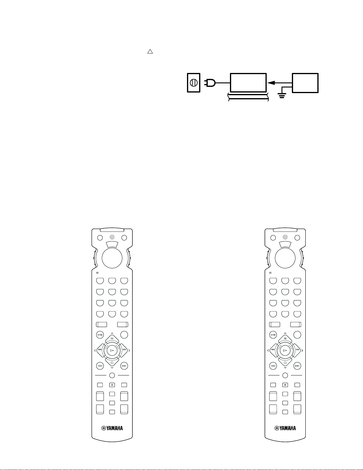
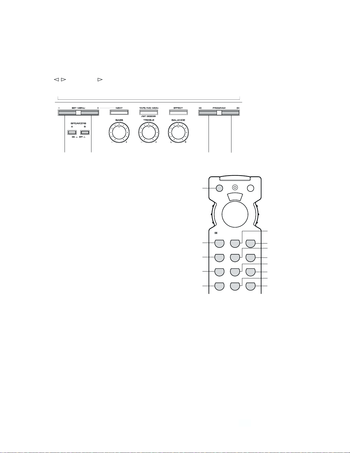
■ REMOTE CONTROL PANELS
▼ R and T models ▼ B and G models
DSP INPUT
/
D
L
D
V
D
/DTS
SUR.
CD
1
MONO MOVIE
DVD/LD
4
ROCK HALL
PHONO
7
EXT.DEC. INDEX
0
--
TEST
DIR A DIR B
POWER
TV
+
--
RAV210
V429760 US
MOVIE
MOVIE
THTR 2
THTR 1
TUNER3TAPE/MD
2
TV SPORTS
DISCO
D-TV6VCR
5
CBL/SAT9V-AUX
8
EFFECT
ENTER >10
A/B/C/D/E
DISC SKIP
PRESET
DISPLAYVCR REC
A/B
E
S
D
E
O
T
C
SELECT
MENUTITLE
POWER
SET MENUTIME/LEVEL
AV
STANDBY
POWER
INPUT
TV
SLEEP
VOLUMETV VOL
MUTE
CHCH
+
I
+
--
DSP INPUT
/
D
L
D
V
D
/DTS
MOVIE
SUR.
THTR 1
TUNER3TAPE/MD
CD
2
1
MONO MOVIE
TV SPORTS
D-TV6VCR
DVD/LD
5
4
ROCK HALL
CBL/SAT9V-AUX
PHONO
8
7
EXT.DEC. INDEX
0
ENTER >10
A/B/C/D/E
DISC SKIP
--
PRESET
TEST
E
S
D
E
O
T
C
DIR A DIR B
SELECT
POWER
AV
STANDBY
POWER
TV
INPUT
TV
+
SLEEP
--
MUTE
MOVIE
THTR 2
DISCO
EFFECT
CHCH
+
DISPLAYVCR REC
A/B
MENUTITLE
SET MENUTIME/LEVEL
POWER
I
+
VOLUMETV VOL
--
RAV211
V429770 EU
1
Page 3
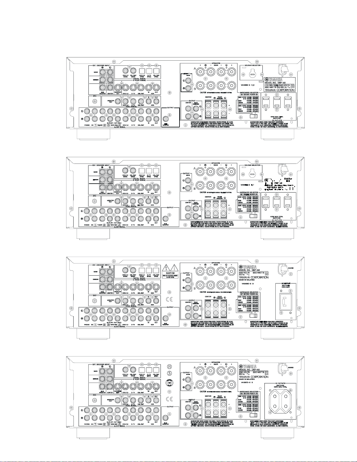
■ REAR PANELS
▼ R model
▼ T model
DSP-A5
▼ B model
▼ G model
2
Page 4
DSP-A5
■ SPECIFICATIONS
■AUDIO SECTION
Minimum RMS Output Power Per Channel
(Power Amp. Section)
MAIN L/R, REAR L/R
20Hz to 20kHz, 0.06% THD, 8Ω 70W+70W
1kHz, 0.09% THD, 8Ω 80W+80W
CENTER
20Hz to 20kHz, 0.06% THD, 8Ω 70W
1kHz, 0.09% THD, 8Ω 80W
Maximum Power (EIAJ)
R, T models only
MAIN L/R, REAR L/R
1kHz, 10% THD, 8Ω 105W+105W
CENTER, 1kHz, 10% THD, 8Ω 105W
Dynamic Power Per Channel (IHF)
MAIN L/R
8/6/4/2Ω
90W+90W/110W+110W/135W+135W/160W+160W
DIN Standard Output Power Per Channel
G model only
MAIN L/R, REAR L/R
1kHz, 0.7% THD, 4Ω 110W+110W
CENTER, 1kHz, 0.7% THD, 4Ω 110W
IEC Power
G model only
MAIN L/R, 1kHz, 0.06% THD, 8Ω 75W+75W
Damping Factor (SPEAKER A)
MAIN L/R, 20Hz to 20kHz, 8Ω 80
Input Sensitivity/Input Impedance
PHONO (MM) 2.5mV/47kΩ
CD etc. 150mV/47kΩ
MAIN L/R (EXTERNAL DECODER) 150mV/47kΩ
CENTER 150mV/40kΩ
SURROUND L/R 150mV/40kΩ
SUB WOOFER 150mV/40kΩ
Maximum Input Signal Level (1kHz)
PHONO (MM), 0.1% THD 100mV
CD etc. (EFFECT ON), 0.5% THD 2.2V
Output Level/Output Impedance
REC OUT 150mV/1.2kΩ
PRE OUT 2.1V/1.2KΩ
SUB WOOFER (MAIN SP : SMALL) 4V/1.2KΩ
Headphone Jack Rated Output/Impedance
CD etc., Input=1kHz, 150mV, RL=8Ω 0.34V/560Ω
Frequency Response(10Hz to 100kHz)
CD etc., MAIN 0/-3dB
RIAA Equalization Deviation
PHONO (MM) 0±0.5dB
Total Harmonic Distortion(20Hz to 20kHz)
PHONO (MM) to REC OUT (1V) 0.02%
CD etc.(EFFECT OFF) to MAIN SP OUT(35W/8Ω)
Signal-to-Noise Ratio(IHF-A Network)
PHONO (MM), Input shorted, REC OUT
R, T models 86dB
B, G models 81dB
CD etc,(EFFECT OFF), Input shorted, SP OUT
0.06%
99dB
Residual Noise(IHF-A Network)
MAIN L/R, SP OUT 150µV
Channel Separation(Vol. –30dB, EFFECT OFF)
PHONO, Input shorted, 1kHz/10kHz 60dB/55dB
CD etc, Input 5.1kΩ terminated, 1kHz/10kHz
60dB/45dB
Tone Control Characteristics
BASS : Boost/Cut ±10dB(50Hz)
: Turnover Frequency 350Hz
TREBLE : Boost/Cut ±10dB(20kHz)
: Turnover Frequency 3.5kHz
Filter Characteristics
MAIN, REAR SP SMALL : H.P.F. fc=90Hz, 12dB/oct.
SUB WOOFER : L.P.F. fc=90Hz, 18dB/oct.
■VIDEO SECTION
Video Signal Type
R model NTSC/PAL
T, B, G models PAL
Video Signal Level 1Vp-p/75Ω
S-Video Signal Level Y:1Vp-p/75Ω,C:0.286Vp-p/75Ω
Maximum Input Level 1.5Vp-p
Signal-to-Noise Ratio 50dB
Monitor Output Frequency Response(–3dB) 5Hz~10MHz
■GENERAL
Power Supply
R model AC110/120/220/240V, 50/60Hz
T model AC220V, 50Hz
B, G models AC230V, 50Hz
Power Consumption
R, T models 310W
B, G models 300W
Standby Power Consumption
B, G models 0.89W
Maximum Power Consumption
R model only
5CH Simultaneous output, 10% THD 510W
AC Outlet
R, T models, Switched x 3 100W max(Total)
B model, Switched x 1 100W max
G model, Switched x 2 100W max(Total)
Dimensions(W x H x D) 435 x 151 x 390.5mm
(17-1/8" x 5-15/16" x 15-3/8")
Weight 11.2kg(24Ibs. 11 oz)
Accessories Remote Control Transmitter x 1
Battery (size "AAA", "R03") x 4
* Specifications subject to change without notice.
R ......... General model B ......... British model
T.......... China model G ......... European model
R,T models→ GD (Gold model)
•
B model
•
G model
•
→
BL (Black model)
→
BL (Black model) and TI (Titan model)
3
Page 5
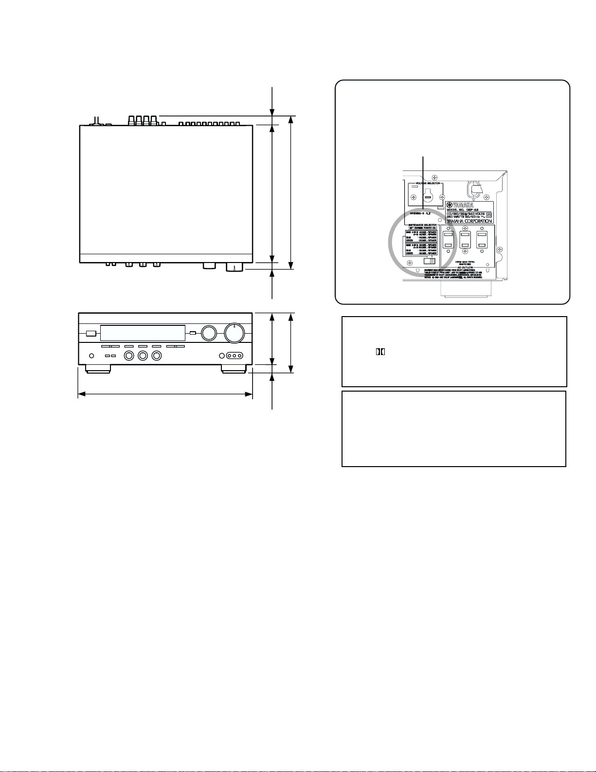
● DIMENSIONS
WARNING
Do not change the IMPEDANCE SELECTOR switch
setting while the power to this unit is on, otherwise
this unit may be damaged.
IMPEDANCE SELECTOR
Manufactured under license from Dolby Laboratories.
"DOLBY", "AC-3", "PRO LOGIC", and the double-D
symbol are trademarks of Dolby Laboratories.
Confidential unpublished works.
©1992-1997 Dolby Laboratories. All rights reserved.
Manufactured under license from Digital Theater
Systems, Inc. US Pat. No. 5,451,942 and other worldwide patents issued and pending. "DTS", "DTS
Digital Surround", are trademarks of Digital Theater
Systems, Inc. Copyright 1996 Digital Theater
Systems, inc. All rights reserved.
21.5
(7/8")
390.5(15-3/8")
349.5(13-3/4")
19.5
(13/16")
DSP-A5
435(17-1/8")
130(5-3/32")
151(5-15/16")
21
(27/32")
Units: mm (inch)
4
Page 6
DSP-A5
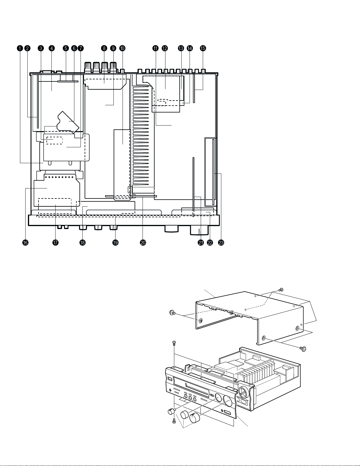
■ INTERNAL VIEW
1 POWER TRANSFORMER
2 P.C.B. POWER (2)
3 P.C.B. POWER (7)
(B,G models only)
4 P.C.B. MAIN (3)
5 P.C.B. POWER (6)
(R,T models only)
6 P.C.B. MAIN (4)
7 P.C.B. POWER (4)
(R,T models only)
8 P.C.B. MAIN (2)
9 P.C.B. MAIN (1)
0 P.C.B. POWER (3)
A P.C.B. INPUT (1)
B P.C.B. INPUT (4)
C P.C.B. INPUT (3)
D P.C.B. INPUT (2)
E P.C.B. INPUT (5)
F P.C.B. POWER (5)
G P.C.B. MAIN (5)
H P.C.B. OPERATION (3)
I P.C.B. OPERATION (1)
J P.C.B. MAIN (6)
K P.C.B. POWER (1)
L P.C.B. OPERATION (2)
M P.C.B. DSP
■ DISASSEMBLY PROCEDURES
(Remove parts in disassembly order as numbered.)
1. Removal of Top Cover
Remove 4 screws (1) and 4 screws (2) in Fig. 1.
2. Removal of Front Panel
a. Remove 5 knobs.
b. Remove 6 screws (3) in Fig. 1.
Top Cover
11
1
11
33
3
33
33
3
33
Knobs
Front Panel
22
2
22
11
1
11
Fig.1
5
Page 7
■
SELF DIAGNOSIS FUNCTION
1. PURPOSE AND OPERATION
The DSP-A5 has a Self Diagnosis Function to locate a faulty part, if any,
by inspecting and taking measurements.
There are 12 main items in the diagnostic menu and have sub-menu items as listed below.
DSP-A5
No.
1
2
3
4
5
6
7
8
9
10
11
12
MAIN MENU
ANALOG THROUGH
DSP THROUGH
AC–3/DTS THROUGH
PRO LOGIC
SPEAKERS SET
DISPLAY CHECK
(EFFECT OFF)
MANUAL TEST
FACTORY PRESET
AD DATA CHECK
STATUS
INFORMATION
FROM DSP
EEPROM WRITING
FUNCTION
UNIT INFORMATION/
EXIT
SUB-MENU
1. MAIN BYPASS
2. DSP 0dB
1. YSS+SRAM M
2. YSS M
3. DSP FULL BIT
1. STATUS (BINARY FORM)
1. CENTER LARGE
2. EFFECT OFF
1. MAIN : SMALL 0dB
2. MAIN : LARGE 0dB
3. MAIN : LARGE –10dB
4. LFE/BASS : MAIN
CENTER : NONE
5. LFE/BASS : MAIN
6. LFE/BASS : SUBWOOFER
7. CENTER : NONE
8. CENTER : SMALL
REAR : SMALL
9. FRONT MIX
1. (EFFECT OFF)
2. ALL SEGMENTS TURN OFF
3. ALL SEGMENTS TURN ON
4. ALTERNATE SEGMENTS TURN ON
5. SOFTWARE RELEASE DATE
1. ALL
2. MAIN L
3. CENTER
4. MAIN R
5. REAR R
6. REAR L
7. LFE
1. INHIBIT (Inhibit Memory Initialize)
2. RESERVED (Reserve Memory Initialize)
1. – – –
2. KEY1, KEY2
3. TUNER SIGNAL LEVEL
4. DC PROTECTION
5. PS PROTECTION
1./2. DSP STATUS (1)/(2)
3./4. CHANNEL STATUS (1)/(2)
5./6. BSI0 (1)/(2)
7./8. BSI1 (1)/(2)
9./10. BSI2 (1)/(2)
11./12. BSI3 (1)/(2)
13./14. BSI4 (1)/(2)
15./16. BSI5 (1)/(2)
1. CHECK SUM
MODIFICATION DATA
EEPROM DATA
2. WRITING CONFIRMATION
3. START WRITING
1. VERSION and CHECK SUM
2. MODEL TYPE and DESTINATION
3. EXIT
REMOTE CONTROL CODE (KEY)
7A–88 ("1" [DSP mode])
– – –
7A–89 ("2" [DSP mode])
– – –
– – –
– – –
7A–8A ("3" [DSP mode])
– – –
7A–8B ("4" [DSP mode])
7A–8C ("5" [DSP mode])
7A–8D ("6" [DSP mode])
7A–8E ("7" [DSP mode])
7A–8F ("8" [DSP mode])
7A–90 ("9" [DSP mode])
7A–91 ("0" [DSP mode])
– – –
7A-12 ("ENTER" [DSP mode])
7A-56 (">10" [DSP mode])
– – –
– – –
– – –
– – –
– – –
– – –
– – –
– – –
– – –
– – –
– – –
– – –
– – –
– – –
– – –
– – –
– – –
– – –
– – –
– – –
– – –
– – –
– – –
– – –
– – –
– – –
– – –
– – –
– – –
– – –
– – –
– – –
6
Page 8
DSP-A5
2. BEGINNING AND CANCELLATION
(1) Starting up the function and the display
After starting up, main menu No.1 is selected.
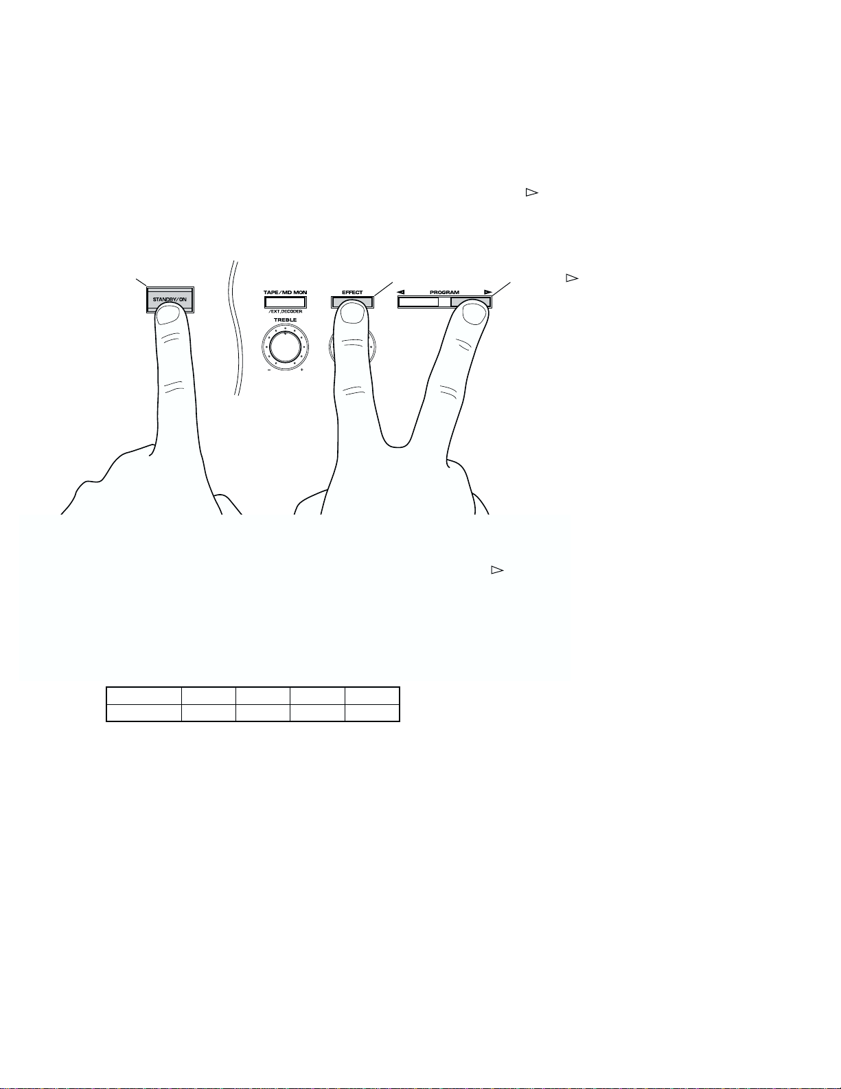
A. How to start diagnostic program
Using the front panel keys of the main unit
Plug in the AC power cord. With the Power OFF,
simultaneously (Step 1), then press the "STANDBY/ON" key (Step 2).
Sub menu No. 1 of the diagnosis main menu No. 1 will start.
FRONT PANEL
hold down the "PROGRAM " and "EFFECT" keys
"STANDBY/ON" key
"EFFECT" key
Step2. Press the "STANDBY/ON" key. Step1. Hold down the "PROGRAM "
and "EFFECT" key simultaneously.
B. Settings for start-up of diagnostic program
The settings used when starting the diagnostic program are as follows.
1.
EFFECT LEVEL :
CHANNEL CENTER R SUR L SUR SWFR
LEVEL (dB) 0 0 0 0
"PROGRAM " key
2.
MUTING : OFF
3.
INPUT (VIDEO) : DVD/LD (DVD/LD)
4.
CENTER SPEAKER : LARGE
5.
REAR SPEAKER : LARGE
6.
MAIN SPEAKER : LARGE
7.
LFE/BASS OUT : SWFR
C. Start-up display
The protection history information appears on the front panel display.
7
Page 9

● FL display at start-up of diagnostic program
When the diagnostic program has started, the check sum of the main microcomputer or the protection history (*1) is
displayed. If the protection function has been activated in the past, the type and voltage value are displayed. After
a few seconds the diagnosis function menu will appear.
(*1) If a faulty condition is detected such as excessive current, a bad power supply or excessive amplifier DC offset,
the Power will be switched OFF automatically.
Note) For the voltages of the power and DC protection functions, see the diagnosis main menu No. 9, which will be
described later. The protection history will be cleared when "RESERVED" is selected in the diagnosis main
menu No. 8 and FACTORY PRESET is engaged.
● Protection history
The following examples show how the protection history is displayed:
DSP-A5
CHK S UM : X X X X X
IPROTECTION
PS PRT : XX%
DC PRT : XX%
Appears when the protection function has not been activated.
Displayed the check sum (4-digit, hexadecimal) and the version
(one letter) of the main microcomputer.
Appears when the current protection function has been activated.
When power is turned on in an abnormal condition, the power relay
will come on, protection will operate immediately, and power will
turn off.
Appears when the power supply protection function has been
activated.
For the % value, the voltage at that point is shown by 5V/100%.
When power is turned on in an abnormal condition, power will turn
off after half a second.
Appears when the power amp DC protection function has been
activated.
For the % value, the voltage at that point is shown by 5V/100%.
When power is turned on in an abnormal condition, power will turn
off after two seconds.
(2) Exiting method
The diagnosis function can be exited by any of the following procedures. Take care with the setting of backup memory
initialization menu (diagnosis No. 8) when releasing the diagnosis function.
1. Select sub-menu No. 3 "EXIT" of the diagnosis main menu No. 12.
2. Press the "STANDBY/ON" key on the main unit or "STANDBY" key on the remote control to turn Power OFF.
8
Page 10
DSP-A5
3. OPERATION AND DISPLAY WHEN STARTING DIAGNOSIS FUNCTION
(1) Selection of diagnostic menu
The diagnostic menu and the sub-menu can be selected by using the front panel keys of the main unit or the remote
control unit.
● Selection by using the front panel keys of the main unit
The main menu can be changed cyclically by using the "SET MENU –/+" keys, and the sub-menu, by using the
"PROGRAM / " keys. The " " key will increase the main or sub-menu number.
FRONT PANEL
Reverse Forward Reverse Forward
Main menu Sub-menu
● Selection by using the remote control unit
The remote control codes in the menu list (see right column
on page 8) correspond to the DSP program, test and effect keys.
See the figure on the right.
7A
DSP INPUT
/
D
L
D
V
D
88
8B
8E
(2) Other functions available while diagnosis function is active
Listed below are the other functions available while the diagnosis function is active.
• Selection of the input (include TAPE MONITOR/EXTERNAL DECODER)
• Effect level control (CENTER, REAR, SUBWOOFER)
• Master volume control
• Muting on/off
• Power on/off
(3) Diagnosis default status
When not otherwise specified, default settings and values in each menu are as follows:
• SPEAKERS : All "LARGE"
• Electronic Volumes : All "0dB"
• DYNAMIC RANGE : MAX
• LFE LEVEL : 0dB (–10dB in AC-3(DOLBY DIGITAL))
• CENTER DELAY : 0ms
/DTS
MOVIE
SUR.
THTR 1
TUNER3TAPE/MD
CD
1
MONO MOVIE
TV SPORTS
DVD/LD
4
ROCK HALL
CBL/SAT9V-AUX
PHONO
7
EXT.DEC. INDEX
0
A/B/C/D/E
MOVIE
THTR 2
2
DISCO
D-TV6VCR
5
8
EFFECT
ENTER >10
89
8A
8C
8D
8F
90
12
5691
9
Page 11

4. CONTENTS OF DIAGNOSIS FUNCTION
This section describes the contents of the Self Diagnosis Function in detail.
No.1 ANALOG THROUGH
The input is fixed to analog (A/D). There are two sub-menus.
DSP-A5
1. MAIN BYPASS
1MAIN BYPASS
The L/R signals bypass the digital circuit, and are output to the MAIN L/R.
The L/R signals are output without being processed to the CENTER/SUBWOOFER, FRONT L/R and REAR L/R
through the DSP. (Remote control code 7A-88: "1" key [DSP mode])
CODEC.ADC
ANALOG IN
AC3D2av(YSS918)
L/R
DAC
MAIN L
MAIN R
AK4324
AK4526A
DECODER
DIR5
DIGITAL IN
YSD917
DOLBY DIGITAL
or
PRO LOGIC
or
DTS
: This shows that the device is not operating.
2. DSP 0dB
1DSP 0dB
The L/R signals are output without being precessed to the MAIN L/R through the AC3D2av.
The L/R signals are output without being precessed to the CENTER/SUBWOOFER, FRONT L/R and REAR L/R through
the DSP.
DSP
L/R L/R
L/R
L/R
1M SRAM
CODEC.DAC
AK4526A
• INPUT : DVD/LD (Analog signal)
(Lch and Rch, 1KHz, –20dBV)
• OUTPUT : SPEAKERS
MAIN L : 24.0 dBV REAR L : 24.0 dBV
MAIN R : 24.0 dBV REAR R : 24.0 dBV
CENTER: 24.0 dBV
FRONT L
FRONT R
CENTER
SUBWOOFER
REAR L
REAR R
CODEC.ADC
ANALOG IN
AK4526A
DIR5
DIGITAL IN
YSD917
: This shows that the device is not operating.
AC3D2av(YSS918)
DECODER
DOLBY DIGITAL
or
PRO LOGIC
or
DTS
L/R L/R
DSP
1M SRAM
L/R
DAC
AK4324
CODEC.DAC
L/R
L/R
• INPUT : DVD/LD (Analog signal)
• OUTPUT : SPEAKERS
AK4526A
(Lch and Rch, 1KHz, –20dBV)
MAIN L : 24.0 dBV REAR L : 24.0 dBV
MAIN R : 24.0 dBV REAR R : 24.0 dBV
CENTER: 24.0 dBV
SUBWOOFER
MAIN L
MAIN R
FRONT L
FRONT R
CENTER
REAR L
REAR R
10
Page 12

DSP-A5
No.2 DSP THROUGH
The input is automatically discriminated by signal detection and switched with priorities Coaxial>Optical>Analog.
There are the following three sub-menus.
1. YSS+SRAM
2 YSS+SRAM M
The L/R signals are output without being processed to the MAIN L/R through the AC3D2av.
The L/R signals are output without being processed to the CENTER/SUBWOOFER through the DSP.
The (L+R)/2 signals are output to the FRONT L/R and REAR L/R through the DSP and the SRAM.
When one of the L/R signals is not input, the output level is –6dB. (Remote control code 7A-89:"2" key [DSP mode])
CODEC.ADC
ANALOG IN
AC3D2av(YSS918)
L/R
DAC
AK4324
MAIN L
MAIN R
AK4526A
DECODER
DOLBY DIGITAL
or
PRO LOGIC
or
DTS
DIGITAL IN
2. YSS M
DIR5
YSD917
2 YSS M
Same as "2. DSP 0dB" of "No.1 ANALOG THROUGH", except for the input switching.
L/R
DSP
(L+R)/2(L+R)/2
1M SRAM
L/R
L/R
(L+R)/2
CODEC.DAC
AK4526A
• INPUT : DVD/LD (Analog signal)
(Lch and Rch, 1KHz, –20dBV)
• OUTPUT : SPEAKERS
MAIN L : 24.0 dBV REAR L : 24.0 dBV
MAIN R : 24.0 dBV REAR R : 24.0 dBV
CENTER: 24.0 dBV
FRONT L
FRONT R
CENTER
SUBWOOFER
REAR L
REAR R
CODEC.ADC
ANALOG IN
AC3D2av(YSS918)
L/R
DAC
AK4324
MAIN L
MAIN R
AK4526A
DECODER
DIR5
DIGITAL IN
YSD917
DOLBY DIGITAL
or
PRO LOGIC
or
DTS
: This shows that the device is not operating.
3. DSP FULL BIT
2DSP FULL BIT
Same as the above menu, except that the head margin is disabled, and the digital data is output with full bits from
AC3D2av to DAC.
DSP
L/R L/R
L/R
L/R
1M SRAM
CODEC.DAC
AK4526A
• INPUT : DVD/LD (Analog signal)
(Lch and Rch, 1KHz, –20dBV)
• OUTPUT : SPEAKERS
MAIN L : 24.0 dBV REAR L : 24.0 dBV
MAIN R : 24.0 dBV REAR R : 24.0 dBV
CENTER: 24.0 dBV
• INPUT : DVD/LD (Analog signal)
(Lch and Rch, 1KHz, –30dBV)
• OUTPUT : SPEAKERS
MAIN L : 14.0 dBV REAR L : 23.3 dBV
MAIN R : 14.0 dBV REAR R : 23.3 dBV
CENTER: 17.2 dBV
FRONT L
FRONT R
CENTER
SUBWOOFER
REAR L
REAR R
11
Page 13

No.3 AC-3/DTS THROUGH
The input is digital signal only. AC-3 (DOLBY DIGITAL) or DTS Digital Surround decoding operation is executed,
according to the input source.
bit 7
bit 1
DSP-A5
1. STATUS(BINARY FORM)
3 ST:10001001
AC-3 (DOLBY DIGITAL) decoded signals are output to each channel via AC3D2av.
The AC-3 (DOLBY DIGITAL) signal status data will be displayed in the FL display using a binary number.
CODEC.ADC
ANALOG IN
AC3D2av(YSS918)
L/R
DAC
AK4324
AK4526A
DECODER
DSP
CODEC.DAC
DIR5
DIGITAL IN
DOLBY DIGITAL
or
PRO LOGIC
or
DTS
C/LFEC/LFE
LS/RSLS/RS
SUBWOOFER
AK4526A
YSD917
: This shows that the device is not operating.
AC-3 Status Info. : bit 7 6 5 4 3 2 1 0
(Invalid in DTS) 1 0 0 01001
IEC958 digital data bit
IEC958 commercial-use device bit
IEC958 digital format error
Demodulator muting (without RF signal)
1 for audio other than PCM linear audio
1 during red DTS lock
1 during DTS decode OK
1 during AC-3 decode OK
1M SRAM
MAIN L
MAIN R
CENTER
REAR L
REAR R
No.4 PRO LOGIC
The submenu is switched between PRO LOGIC (AUTO BALANCE OFF) and EFFECT OFF.
1. CENTER LARGE
4PROCNTR:LRG
The input is automatically discriminated by signal detection and switched with priorities Coaxial>Optical>Analog.
DTS Digital Surround is disabled. The input signals are PRO LOGIC decoded and output.
(Remote control code 7A-8A: "3" key [DSP mode])
CODEC.ADC
ANALOG IN
AC3D2av(YSS918)
L/R
DAC
AK4324
AK4526A
DECODER
DSP
CODEC.DAC
DIR5
DIGITAL IN
DOLBY DIGITAL
or
PRO LOGIC
or
DTS
C
S
C
S
AK4526A
YSD917
• INPUT : DVD/LD (Analog signal)
(Lch and Rch, or Lch only, 1KHz, –20dBV)
1M SRAM
2. EFFECT OFF
4PRO EFCT:OFF
The input is only for analog signal. The L/R signals bypass the digital circuit and are output to the MAIN L/R.
• OUTPUT : SPEAKERS
(INPUT : Lch and Rch ) (INPUT : Lch only)
MAIN L : –12.5 dBV MAIN L : 24.0 dBV
MAIN R : –12.5 dBV MAIN R : –19.0 dBV
CENTER: 27.0 dBV CENTER : –10.0 dBV
REAR L : –9.0 dBV REAR L : –9.0 dBV
REAR R : –9.0 dBV REAR R : –9.0 dBV
MAIN L
MAIN R
CENTER
REAR L
REAR R
12
Page 14

DSP-A5
No.5 SPEAKERS SET
The input is automatically discriminated by signal detection and switched with priorities Coaxial>Optical>Analog.
The L/R signals are output to channels specified by the sub-menu without being processed.
There are the following nine sub-menus items. Signal routes of the sub-menu 1-4 are the same as EFFECT OFF.
But MAIN L/R are signals through the digital circuit.
Signal routes of the sub-menu 5-9 are the same as "2. YSS M" of "No. 2 DSP THROUGH".
However, only MAIN L/R are output in the sub-menu 1-4.
5MAIN:SML0dB
5 B:MAIN C:NON
5 C:NONE
5MAIN:LRG0dB
5LFE/B:MAIN
5 C : S REAR: S
5MAIN:LRG -10
5 LFE/B:SWFR
5FRONTMIX
The analog switches in each sub-menu are set as follows:
SUB MENU
1 MAIN:SML 0DB 7A-8B LARGE LARGE SMALL 0dB SWFR L R NONE NONE NONE L+R
2 MAIN:LRG 0DB 7A-8C LARGE LARGE LARGE 0dB SWFR L L NONE NONR NONE NONE
3 MAIN:LRG -10 7A-8D LARGE LARGE LARGE -10dB SWFR L L NONE NONE NONE NONE
4 B:MAIN C:NONE 7A-8E NONE LARGE LARGE 0dB MAIN L L NONE NONE NONE NONE
5 LFE/B:MAIN 7A-8F LARGE LARGE LARGE 0dB MAIN
6 LFE/B:SWFR 7A-90 LARGE LARGE LARGE 0dB SWFR NONE NONE NONE NONE NONE LFE
7 C:NONE 7A-91 NONE LARGE LARGE 0dB SWFR C+L C+R NONE NONE NONE NONE
8 C:S REAR:S – – – SMALL SMALL LARGE 0dB SWFR FL FR C RL RR
9 FRONT MIX 7A-12 LARGE LARGE LARGE 0dB SWFR FL FR NONE NONE NONE NONE
REMOTE
CONTROL
CODE
CENTER SP
MAIN SPREAR SP
MAIN
LEVEL
LFE/BASS
MAIN
MAIN
L
R
LFE+FL LFE+FR
OUTPUTSETTING
REAR
CENTER
NONE NONE NONE NONE
REAR
L
SUB
R
WOOFER
C+RL+RR+LFE
LARGE: Mode in which speakers with high bass-sound playback capability (large unit) are used. Full-range signals present
on the channel are output from the speaker.
SMALL : Mode in which speakers with low bass-sound playback capability (small unit) are used. Low bass signals (below
90Hz) on the channel are mixed into the channel selected by the LFE/BASS setting.
NONE: Mode in which center speaker is not used. The center channel signal is reduced by 3 dB and mixed into MAIN L/R.
LFE/B:MAIN
: Mode in which subwoofer speaker is not used. The LFE channel signal is reduced by 4.5 dB and mixed into
MAIN L/R. But because of the phase difference, the MAIN L/R output is not simply summed.
Description of the submenu as follows:
SUB MENU DESCRIPTION
1 MAIN:SML 0DB Verification of the High and low pass filter response and gain in the bass redirection mode.
2 MAIN:LRG 0DB Reference of the sub menu No. 1 and 3.
3 MAIN:LRG -10 Verification of the effect in the main level function.
4 B:MAIN C:NONE Verification of the mixing circuit effect to the main channel.
5 LFE/B:MAIN Verification of the bass mix gain.
6 LFE/B:SWFR Verification of the LFE maximum output.
7 C:NONE Verification of the center mix gain.
8 C:S REAR:S Verification of the high and low pass filter response and gain in the bass redirection mode.
9 FRONT MIX Verification of the front mix gain.
13
Page 15

No.6 DISPLAY CHECK
Check program for FL display. The display status will change as follows with sub-menu operation.
signal route is the same as "2. EFFECT OFF" of "No. 4 PRO LOGIC".
DSP-A5
6 VFD CHCK
Initial display All segments turn off All segments turn on (See page 29)
A defect of the FL drive port and FL display segments can be detected by using "All segments turn off" and "All
segments turn on".
A short-circuit between adjacent segments can be detected by using "Alternate segments turn on" (lattice form).
No.7 MANUAL TEST
By using the noise generator built into the DSP, a test noise outputs to the channel specified by the sub-menu.
7TESTALL
7TESTMAINR
(lattice form)
Alternate segments turn onSoftware Release date display
7TESTMAINL
7 TEST REAR R
7 TEST CENTER
7 TEST REAR L
7TESTLFE
No.8 FACTORY PRESET
The initialization of the back-up RAM, which contains, the DSP program, set menu contents, etc. is reserved
or inhibited. Signal route is the same as "2. EFFECT OFF" of "No.4 PRO LOGIC".
8PRESET INHI
8 PRESET RSRVD
1. INHIBITED: Inhibits initialization of the back-up RAM.
Specify this option protect user set values.
2. RESERVED: Reserve to initialization of the back-up RAM.
(The RAM is actually initialized when power
is turned on next time.) Specify this option
at the factory preset or to reset the RAM.
For the contents of the initialization, see page 18.
The protection data is also reset.
14
Page 16

DSP-A5
No.9 AD DATA CHECK
The A/D conversion values of the microcomputer which detects key scan port, protection detection port, etc. are displayed
in % (100%:5V). Signal route is the same as "2. EFFECT OFF" of "No. 4 PRO LOGIC".
The keys on the main unit cannot be operated to detect the values of all keys in the K1/K2 and SI.
Operating the "PROGRAM , "key and turning the rotary encoder ("INPUT SELECTOR" on the main unit) will switch the
sub-menu.
9 AD DATA CHK
9 K1 : 100K2 : 100
9SI: 0
9DC: 7
Initial display.
For return to the PS menu, press the "PROGRAM " key.
Press the "PROGRAM " key.
K1/K2: Panel key on the main unit.
(See Table 1.)
Turning the "INPUT SELECTOR".
SI: Tuner signal sensitivity level
For return to the K1/K2 menu, press the "PROGRAM "key.
Press the "PROGRAM " key.
DC: DC protection value
(normal value: 1-13)
For return to the SI menu, press the "PROGRAM "key.
Press the "PROGRAM " key.
PS: Power voltage protection value
(normal value: 23-38)
For return to the DC menu, press the "PROGRAM "key.
For return to the initial display, press the "PROGRAM "key again.
TAPE/MD MON
/EXT DECODER
EFFECT
Table 1
AD Value
K1
K2
9PS: 30
01525354555657585
SET MENU
NEXT
– +
PROGRAM
INPUT MODE
Cautions:
1. If K1 and K2 are more than ±4% from the reference values, normal operation will not be executed.
2. If DC and PS are outside the normal values, the protection function will operate and power will turn off.
15
Page 17

No.10 STATUS INFORMATION FROM DSP
The status data from the DSP block is sequentially displayed in a hexadecimal number.
Signal route is the same as "2. EFFECT OFF" of "No. 4 PRO LOGIC".
High
Low
DSP-A5
[CPU/1]
[CPU/2]
10 CPU/ 1 00 00
10 CHS/ 2 00 00
10 BI2/1 00 00
10 CPU/ 1 00 00
10 BI0/1 00 00
10 BI2/2 00 00
10 CHS/ 2 00 00
10 BI0/2 00 00
10 BI3/1 00 00
10 BI3/2 00 00 10 BI4/1 00 00 10 BI4/2 00 00
10 BI5/1 00 00 10 BI5/2 00 00
<High Byte>
bit7 Mute request bit3 acmod
bit6 fs bit2
bit5
bit4 bit0
[Note]
When acmod is beyond 1000B, it is DTS 7.1 signal. And the DSP block will be muted.
The acmod of DTS 2/0 is as 0000B:1+1.
<Low Byte>
bit7 AC-3 DECODE OK bit3
bit6 DTS DECODE OK bit2 IEC958 digital format error
bit5
bit4
[Note]
IEC958: Standard to identify the PCM bit stream signal. Digital format error refers to a digital signal with the
sampling frequency undefined (neither 32k,44.1k,48k,64k,88.2k nor 96k). Since the operation of each device
cannot be assured at fs outside specifications, this status handled as the forced analog mode (ignored even if
decoding is OK from the detection terminal level), and the signals from the analog input terminal will be
selected. Bits 4-6 of "CPU/1" will be 000B (Analog), and the microcomputer operates in the same way as with
digital unlocking.
<High Byte>
000B:Analog 001B:32kHz
010B:44.1kHz 011B:48kHz
100B:64kHz 101B:88.2kHz
110B:96kHz 111B:undefined
Red DTS record
(Flashes and lights)
1 for audio other than PCM
linear audio
0000B:1+1 0001B:1/0
0010B:2/0 0011B:3/0
0100B:2/1 0101B:3/1
bit1
0110B:2/2 0111B:3/2
1000B:7.1
DEM (Demodulator) MUTE
(without RF signal)
bit1 IEC958 commercial-use device bit
bit0 IEC958 digital data bit
Indicate
bit 7 6 5 4 3 2 1 0
0
0
Indicate bit
3210
7654
0
0000
1
0001
2
0010
3
0011
4
0100
5
0101
6
0110
7
0111
8
1000
9
1001
A
1010
B
1011
C
1100
D
1101
E
1110
F1
111
bit7 AC3 KARAOKE bit3 1
bit6 DIR2 LOCKN bit2 0
bit5 DIR2 ERR bit1 DSP is AC3D2 (DTS present)
bit4 AC3D MUTE bit0 RF DEM (Demodulator) present
<Low Byte> Always “00”
[CHS/1,/2] IEC958 channel status bits 00-31 available from DIR5.
<CHS/1 High Byte> bits 00-07
<CHS/1 Low Byte> bits 08-15
<CHS/2 High Byte> bits 16-23
<CHS/2 Low Byte> bits 24-31
[BI0/1,/2] Displays the bit stream information contained in AC-3(DOLBY DIGITAL)/DTS Digital Surround signal from the first byte.
[BI1-5/1,/2] Displays the bit stream information contained in AC-3(DOLBY DIGITAL) signal from the first byte.
16
Page 18

DSP-A5
No.11 EEPROM WRITING FUNCTION
The check sum value confirmation of EEPROM and data writing.
Signal route is the same as "2. EFFECT OFF" of "No. 4 PRO LOGIC".
M:XXXX E : XXXX
M:XXXX: The check sum value is displayed when the microcomputer has ROM
modification data.
0000 is displayed when there is no data.
E:XXXX: The check sum value is displayed when the EEPROM is installed on and
it has the ROM data .
000 is displayed when EEPROM is not mounted on or data is unusual.
If you want to write ROM modification data of the microcomputer into the
EEPROM, change to the next sub-menu.
No.12 UNIT INFORMATION/EXIT
The version of the microcomputer and the check sum, the model type and the destination are displayed.
Signal route is the same as "2. EFFECT OFF" of "No.4 PRO LOGIC".
By the sub-menu operation, the set exits the self-diagnousis mode and returns to the normal operation mode.
12 A01 824E
Version Check sum
12 RX-V ABGL
Model type Destination
The version and the check sum of the microcomputer software are displayed.
A01: Microcomputer software version.
824E: Microcomputer software check sum.
The model type and the destination are displayed.
RX-V: Model type.
DSP-A= DSP-A5
RX-V = RX-V596, HTR-5250
RDS = RX-V596RDS
ABGL: Destination.
J = J model
UC = U and C models
ABGL = A,B,G and L models
R = R and T model
17
EXIT
Page 19

■ FACTORY PRESET
All of the system settings are initially set from the factory as follows.
●
INPUT SELECTOR
INPUT FACTORY PRESET PROGRAM
PHONO CONCERT HALL
CD DISCO
TUNER ROCK CONCERT
ROTARY DVD/LD SCI-FI
ENCODER D-TV TV SPORTS
VCR DOLBY NORMAL
V-AUX DOLBY ENHANCED
CBL/SAT ROCK CONCERT
MONITOR TAPE/MD EFFECT OFF
EXTERNAL EXT. DECODER NONE
● DSP PROGRAM
No. PROGRAM SUB-PROGRAM DELAY PRESET VALUE
1.
2.
3. 70mm : 20ms, DGTL/DTS : 15ms
4. MONO MOVIE – 49ms
5. TV SPORTS – 9ms
6. DISCO – 40ms
7. ROCK CONCERT – 16ms
8. CONCERT HALL – 44ms
●
SET MENU
No. SET MENU PRESET VALUE
1. CENTER SP SIZE CENTER SP : LRG(LARGE)
2. REAR SP SIZE REAR SP : LARGE
3. MAIN SP SIZE MAIN SP : LARGE
4. BASS OUT MODE BASS OUT : BOTH
5. M. LVL CHOICE MAIN LVL : NRML (NORMAL)
6. D. D. LFE OUT LEVEL D. D. LFE 0 dB
7. D. RNG CHOICE D-RANGE : MAX
8. DTS LFE OUT LEVEL DTS LFE 0 dB
9. C. DELAY CHANGE CENTER DELAY 0ms
10.
11.
12. INPUT MODE CBL/SAT CBL INPUT : AUTO
DOLBY/DTS NORMAL PRO LOGIC : 20ms,
SURROUND ENHANCED DOLBY DIGITAL/DTS DIGITAL SUR : 5ms
MOVIE THEATER SPECTACLE 70mm : 23ms, DGTL/DTS : 15ms
1 SCI-FI 70mm : 20ms, DGTL/DTS : 16ms
MOVIE THEATER ADVENTURE
2 GENERAL
MEMORY GUARD MEM. GUARD : OFF
INPUT MODE D-TV TV INPUT : AUTO
DSP-A5
● EFFECT LEVEL
EFFECT CHANNEL PRESET VALUE
CENTER 0 dB
RIGHT SURROUND 0 dB
LEFT SURROUND 0 dB
SUBWOOFER 0 dB
18
Page 20

DSP-A5
■ AMP ADJUSTMENT
Confirmation of Idling Current of Main Amplifier
Right after power is turned on, confirm that the voltage across the
•
terminals of R688(Main Lch),R690(Main Rch), R692(Center),
R694(Rear Lch), R696(Rear Rch) are between 0.1mV and 10.0mV.
If it exceeds 10.0mV, open (cut off) R571 (Main Lch), R577 (Main
•
Rch), R583 (Center), R589 (Rear Lch), R595 (Rear Rch) and
reconfirm the voltage.
Confirm that the voltage is 0.20mV ~ 15.0mV after 60 minutes.
•
0.1mV ~ 10.0mV
(DC)
MAIN (1)
R577
R692
R694
R690
R696
R583
R595
R589
Q523
Q525
Q524
Q522
R688(Lch)
R690(Rch)
R692(Cch)
R694(RLch)
R696(RRch)
R571(Lch)
R577(Rch)
R583(Cch)
R589(RLch)
R595(RRch)
0.1mV ~ 10.0mV
(DC)
Cut off
19
R571
R688
POWER (3)
Front Panel
Q521
Note)
If R571, R577, R583, R589 and
•
R595 have already been cut off
and idling current does not flow,
reconnect R571, R577, R583,
R589 and R595.
Q521 ~ Q525 are transistors for
•
temperature correction.
Apply silicone grease to contact
surface with the heat sink.
Page 21

■ IC DATA
IC501 : M30217MA-A203FP
16-bit Microcomputer
P67/FL07
P66/FL06
P65/FL05
P64/FL04
P63/FL03
P62/FL02
P61/FL01
P60/FL00
VEE
P107/AN7
P106/AN6
P105/AN5
P104/AN4
P103/AN3
P102/AN2
P101/AN1
AVSS
P100/AN0
VREF
AVCC
81
82
83
84
85
86
87
88
89
90
91
92
93
94
95
96
97
98
99
100
P50/FL08
P51/FL09
P52/FL10
P53/FL11
P54/FL12
P55/FL13
P56/FL14
P57/FL15
P00/FL16
P01/FL17
P02/FL18
P03/FL19
P04/FL20
TOP VIEW
1110987654321
P05/FL21
P06/FL22
VSS
P07/FL23
VCC
P10/FL24
61626364656667686970
201918171615141312
P11/FL25
P12/FL26
P13/FL27
P14/FL28
P15/FL29
P16/FL30
P17/FL31
P20/FL32
P21/FL33
P22/FL34
P23/FL35
5152535455565758596071727374757677787980
50
49
48
47
46
45
44
43
42
41
40
39
38
37
36
35
34
33
32
31
30292827262524232221
DSP-A5
P24/FL36
P25/FL37
P26/FL38
P27/FL39
P30/FL40
P31/FL41
P32/FL42
P33/FL43
P34/FL44
P35/FL45
P36/FL46
P37/FL47
P40/FL48
P41/FL49
P42/FL50
P43/FL51
P44/FL52
P45/FL53
P46/FL54
P47/FL55
P00/FL16~
P07/FL22
77-66,64
P10/FL24~
P17/FL31
62-55
I/O PORT
PORT 0
(P00-07)
PORT 1
(P10-17)
INTERNAL PERIPHERAL
FUNCTION
TIMER
TIMER A0 (16-bit)
TIMER A1 (16-bit)
TIMER A2 (16-bit)
TIMER A3 (16-bit)
TIMER A4 (16-bit)
TIMER B0 (16-bit)
TIMER B1 (16-bit)
TIMER B2 (16-bit)
SUPERVISOR TIMER
(15-bit)
DMAC
(2-ch)
D/A CONVERTER
(8-bit x 2-ch)
P97
P96
P95/CK2
P94/SO2
PP93/SI2
P20/FL32~
P27/FL39
54-47
PORT 2
(P20-27)
P92
P91
P90
P30/FL40~
P37/FL47
46-39
PORT 3
(P30-37)
P87
CNVSS
P40/FL48~
P47/FL55
PORT 4
(P40-47)
P86
38-31
XOUT
/RESET
XIN
VSS
VCC
P50/FL08~
P57/FL15
80-73
PORT 5
(P50-57)
P85/INT5
A/D CONVERTER
(10-bit x 8-ch)
SERIAL I/O
UART0,1(UART/
CLOCK SYNCHRONOUS)
(8-bit x 2-ch)
SI/O2(CLOCK SYNCHRONOUS)
(256-Byte AUTOMATIC TRANSFER)
M16C/60 SERIES CPU CORE
(16-bit)
REGISTER
R0H R0L
R0H R0L
R1H R1L
R2
R3
A0
A1
FB
SB
STACK POINTER
VECTOR TABLE
MULTIPLIER
P84/INT4
P83/INT3
P82/INT2
P60/FL00~
P67/FL07
88-81
PORT 6
(P60-67)
ISP
USP
INTB
P77
P81/INT1
P80/INT0
P70~P73,
P74/TX1,
P75/RX1,
P76/CK1,
P77
30-23
PORT 7
(P70-77)
P74/TX1
P76/CK1
P76/RX1
P80/INT1~
P85/INT5
P86,P87
22-17,11,10
PORT 8
(P80-87)
P73
P72
P71
P70
P90~P92,
P93/SI2,
P94/SO2,
P95/CK2,
P96,P97
PORT 9
(P90-97)
8-1
P100/AN0~
P107/AN7
98,96-90
PORT 10
(P100-107)
SYSTEM CLOCK GENERATOR
(2-ch)
XIN-XOUT
XCIN-XCOUT
CRC PROCESSOR (CCITT MODE)
(GENERATION MULTINOMIAL:
15+X12+X5
X
+1)
VFD CONTROLLER (8-bit x 7)
MEMORY
ROM
RAM
(FLDC, ASI/ORAM)
16,63
VCC89VEE
14,65
VSS9CNVSS
FOR ANALOG CIRCUIT
100
AVCC
99
VREF97AVSS
SYSTEM RESET SYSTEM CLOCK
12
/RESET
15
XIN13XOUT
20
Page 22

DSP-A5
IC501 : M30217MA-A203FP
16-bit Microcomputer
Pin Pin
Port I/O Function
No. Name
1 P97 SCK O Serial Clock output
2 P96 SDT O Serial Data output
For Input
selector Tuner,
etc.
3 P95 RCK O Clock output for model type
/CK2 distinction (*1)
4 P94 RDT O Data output for destination distinction
/SO2 of Tuner (*2)
5 P93 DEST O Data input for destination distinction
/SI2 /RD0 of Tuner (*2)
6 P92 RCE O Chip enable output for model type
distinction (*1)
7 P91 SCKD O Serial Clock output for DIR5
8 P90 SID O Serial data output for DIR5
9 CNVSS CNVSS For flash µ-COM write connector
10 P87 CKB O Clock output for output port
expansion IC
11 P86 DTB O Data output for output port
expansion IC
12 /RESET /RES System reset
13 XOUT XOUT Crystal oscillator connected (10MHz)
14 VSS MG Ground
15 XIN MU Crystal oscillator connected (10MHz)
16 VCC +5BU +5V Power supply
17
18
19
20
21
22
P85/INT5
P84/INT4
P83/INT3
P82/INT2
P81/INT1
P80/INT0
INTD I Interrupt factor detect input from DIR5
ERRA I Data mute detect input from AC3D2av
REM I Remote control input
PDT I Power down detect input
PSW I Standby switch input
DBL I Double speed sampling mode
selection data input DIR5
23 P77 CEAC2 O Chip enable output 2 for AC3D2av
24 P76/CK1 CLKAC O Serial clock output for AC3D2av
25 P75/RX1 RXAC I Serial data input from AV3D2av
26 P74/TX1 TXAC O Serial data output for AC3D2av
27 P73 CEAC1 O Chip enable output 1 for AC3D2av
28 P72 TCE O Chip enable output for Tuner
29 P71 CELC O Chip enable output for Input Selector
30 P70 CETC O Chip enable output for Input Selector
Pin Pin
Port I/O Function
No. Name
31
32
33
34
35
36
37
38
39
40
P47/FL55
P46/FL54
P45/FL53
P44/FL52
P43/FL51
P42/FL50
P41/FL49
P40/FL48
P37/FL47
P36/FL46
F-CE O Chip enable output
F-CK O Serial clock output
F-RX I Serial data input
F-TX O Serial data output
VUP O Volume up output
VDN O Volume down output
SOD I Serial data input from DIR5
CECOD O Chip enable output for CODEC
/CSD O Chip select output for DIR5
PRI I I (Over current) protection
detect input
41
42
43
44
45
46
47
48
49
50
51
52
53
54
55
56
57
58
59
60
61
62
P35/FL45
P34/FL44
P33/FL43
P32/FL42
P31/FL41
P30/FL40
P27/FL39
P26/FL38
P25/FL37
P24/FL36
P23/FL35
P22/FL34
P21/FL33
P20/FL32
P17/FL31
P16/FL30
P15/FL29
P14/FL28
P13/FL27
P12/FL26
P11/FL25
P10/FL24
POT-A I Rotary encoder input A
POT-B I Rotary encoder input B
/ST I Stereo input from Tuner
DO I Serial data input from Tuner
/ICD O Initial clear output for DIR5
PRY O Power relay output
SRY O Speaker relay output
ERY O Effect relay output
G1 O Grid 1 for FL display
G2 O Grid 2 for FL display
G3 O Grid 3 for FL display
G4 O Grid 4 for FL display
G5 O Grid 5 for FL display
G6 O Grid 6 for FL display
G7 O Grid 7 for FL display
G8 O Grid 8 for FL display
G9 O Grid 9 for FL display
G10 O Grid 10 for FL display
G11 O Grid 11 for FL display
G12 O Grid 12 for FL display
G13 O Grid 13 for FL display
G14 O Grid 14 for FL display
63 VCC +5VBU +5V power supply
64
P07/FL23
G15 O Grid 15 for FL display
65 VSS MG Ground
66
P06/FL22
G16 O Grid 16 for FL display
For
flash µ-COM
write
connector
*1 Model type distinction (H=1, L=0)
DSP-A (Pin 3) 0 0 1 RX-V596 1 RX-V596RDS
RDS (Pin 6) 0 1 0 HTR-5250 1
DSP-A5 DSP-E
*2 Destination distinction of Tuner (H=1, L=0)
V1 (Pin 4) 0 J 0 U,C 1 A,B,G,L 1 R,T
V2 (Pin 5) 0 model 1 models 0 models 1 models
21
Page 23

IC501 : M30217MA-A203FP
16-bit Microcomputer
DSP-A5
Pin Pin
Port I/O Function
No. Name
67
68
69
70
71
72
73
74
75
76
77
78
79
80
81
82
83
84
P05/FL21
P04/FL20
P03/FL19
P02/FL18
P01/FL17
P00/FL16
P57/FL15
P56/FL14
P55/FL13
P54/FL12
P53/FL11
P52/FL10
P51/FL09
P50/FL08
P67/FL07
P66/FL06
P65/FL05
P64/FL04
P1 O Segment 1 for FL display
P2 O Segment 2 for FL display
P3 O Segment 3 for FL display
P4 O Segment 4 for FL display
P5 O Segment 5 for FL display
P6 O Segment 6 for FL display
P7 O Segment 7 for FL display
P8 O Segment 8 for FL display
P9 O Segment 9 for FL display
P10 O Segment 10 for FL display
P11 O Segment 11 for FL display
P12 O Segment 12 for FL display
P13 O Segment 13 for FL display
P14 O Segment 14 for FL display
P15 O Segment 15 for FL display
P16 O Segment 16 for FL display
P17 O Segment 17 for FL display
P18 O Segment 18 for FL display
IC107 : BU2090
Serial Input/Parallel Output Driver for Output port expansion
Pin Pin
Port I/O Function
No. Name
85
86
87
88
89
90
91
P63/FL03
P62/FL02
P61/FL01
P60/FL00
VEE
P107/AN7
P106/AN6
P19 O Segment 19 for FL display
P20 O Segment 20 for FL display
P21 O Segment 21 for FL display
P22 O Segment 22 for FL display
VP O Power supply for FL display
LIMDT I Limitter DC detect input
PRV I PS (power voltage) protection
AD value detect input
92
P105/AN5
PRD I DC (power amp voltage) protection
AD value detect input
93
94
95
96
P104/AN4
P103/AN3
P102/AN2
P101/AN1
METER I Tuner meter AD value input
NC O No connection
/FMT O Full mute output (L: ON)
KEY2 I Key 2 AD data value input
97 AVSS MG Ground
98
P100/AN0
KEY1 I Key 1 AD data value input
99 VREF +5M Standard power supply for AD input
100 AVCC +5BU +5V power supply
VSS
DATA
CLOCK
Q0
Q1
Q2
Q3
Q4
Pin Pin
Port I/O Function
1
16
VDD
No. Name
1 VSS VSS Ground
2
3
CONTROL
LOGIC
15
14
Q11
Q10
2 DATA DTB I Control data input
3 CLOCK CKB I Control clock input
4 Q0 SW1 O Video select data
5 Q1 SW2 O output 1-5(*)
from
microcomputer
for
video input
selector
6 Q2 SW3 O
4
12
Q9
7 Q3 SW4 O
8 Q4 SW5 O
5
6
OUTPUT BUFFER
7
LATCH
(OPEN DRAIN)
12-Bit SHIFT REGISTER
12
11
10
Q8
Q7
Q6
9 Q5 /CONT1 O Limitter control data output 1,2
10 Q6 /CONT2 O
11 Q7 /-10dB O –10dB control data output
(L : –10dB)
12 Q8 /ICAC O Initial clear output for AC3D2av
13 Q9 NC O Unconnected
8
9
Q5
14 Q10 NC O Unconnected
15 Q11 /T-MUTE O Tuner mute data output (L : Mute on)
(TOP VIEW)
16 VDD VDD +5V power supply
* Video input
Selector
Control
(H=High,
L=Low,
X=Don't care)
Video Input SW1 SW2 SW3 SW4 SW5
(Pin4) (Pin5) (Pin6) (Pin7) (Pin8)
CBL/SAT H L X L H
D-TV H H X L H
DVD/LD H L L H H
VCR L H X X H
V-AUX H L H H H
OFF L L X X L
22
Page 24

DSP-A5
IC3 : YSD917 (DIR5)
Digital Format Interface Receiver
AVDD
PCO
AVSS
M/S
DDIN
TEST
/IC
VSS
XO
MCK
VDD
SDO
SDBCK
1
2
3
4
5
6
7
8
9
10
XI
11
12
13
14
TOP VIEW
28
27
26
25
24
23
22
21
20
19
18
17
16
15
SCK
SI
SO
/CS
VDD
INT
/LOCK
ERR
DBL
FS128
SYNC
VSS
SDMCK
SDWCK
DDIN
/IC
5
7
/LOCK
PCO
GENERATION
DATA BU S
XIXOMCK
STANDARD
CLOCK
CHANNEL
STATUS
USER DATA
FRAME
BUFFER
SELECTION
22 2 10 9 11 4
PLL
DECODER &
LOCK ERROR JUDGMENT
DIGITAL AUDIO INTERFACE
EACH CONTROL
SIGNAL
MICROPROCESSOR
INTERFACE
CLOCK
SYSTEM
OUTPUT
CLOCK
GENERATION
SERIAL
CONVERSION
INTERRUPT
FACTOR
DETECTION
M/S
OUTPUT
SELECTION
16
15
14
18
19
20
21
13
SDMCK
SDWCK
SDBCK
SYNC
FS128
DBL
ERR
SDO
26
SO
Pin Pin
No. Name
I/O Function
1 AVDD Power supply
2 PCO I/O PLL phase comparison output
3 AVSS Ground
4 M/S I Unconnected
5 DDIN I Digital audio data input
6 TEST Unconnected
7 /IC I Initial clear input from microcomputer
8 VSS Ground
9 XO O Crystal oscillator connection (24.576MHz)
10 XI I Crystal oscillator connection (24.576MHz)
11 MCK O Master clock output for AC3D2av
12 VDD Power supply
13 SDO O Serial audio data output for AC3D2av
14 SDBCK I/O 64fs bit clock output for microcomputer,
CODEC, DAC
15 SDWCK I/O 1fs word clock output for microcomputer,
CODEC, DAC
16 SDMCK O 256fs bit clock output for microcomputer,
CODEC, DAC
28 23
2725
SI
/CS
SCK
Pin Pin
No. Name
I/O Function
INT
17 VSS Ground
18 SYNC O Unconnected
19 FS128 O Unconnected
20 DBL O Double speed sampling mode selection data
output for microcomputer, CODEC, DAC
21 ERR O Unconnected
22 /LOCK O Unconnected
23 INT O Interrupt factor detect output for
microcomputer
24 VDD Power supply
25 /CS I Chip select input from microcomputer
26 SO O Serial data output for microcomputer
27 SI I Serial data input for microcomputer
28 SCK I Serial clock input from microcomputer
23
Page 25

IC4 : YSS918D-F (AC3D2av)
DSP + AC-3(Dolby Digital)/ Pro Logic/ DTS Digital Surround Decoder
VSS
RAMD7
RAMD6
RAMD5
RAMD4
RAMD3
RAMD2
RAMD1
RAMD0
VDD1
RAMA2
SCKSISO
/CS
/CSB
RAMA3
64656667686970
81
VDD
SDWCK0
SDBCK0
SDIA0
SDIA1
RAMA1
RAMA0
RAMWEN
RAMOEN
IPORT7
IPORT6
IPORT5
IPORT4
IPORT3
IPORT2
IPORT1
IPORT0
VSS
VDD
VSS
82
83
84
85
86
87
88
89
90
91
92
93
94
95
96
97
98
99
100
VDD1
RAMCEN
54321
SDIB0
RAMA16
RAMA15
SDIB1
SDIB2
TOP VIEW
XI
XO
VSS
AVDD
TEST
TEST
OVFB
SDIB3
AC3DATA
DTSDATA
TEST
/IC
616263
20191817161514131211109876
CPO
SDOB3
RAMA4
VSS
VDD
AVSS
RAMA5
RAMA6
SDOA2
SDOA1
/SDBCK0
SURENC
KARAOKE
5455565758596071727374757677787980
SDOA0
RAMA14
RAMA13
MUTE
CRC
NONPCM
RAMA11
RAMA12
RAMA10
VDD2
515253
50
49
48
47
46
45
44
43
42
41
40
39
38
37
36
35
34
33
32
31
30292827262524232221
VSS
DSP-A5
PVSS
SDWCK1
SDBCK1
SDOB0
SDOB1
SDOB2
RAMA7
RAMA8
RAMA9
VDD2
VSS
OPORT7
OPORT6
OPORT5
OPORT4
OPORT3
OPORT2
OPORT1
OPORT0
VDD1
/SDBCK0
SDBCK0
SDWCK0
SDIA0
SDIA1
SURENC
KARAOKE
MUTE
CRC
AC3DATA
DTSDATA
NONPCM
57
83
82
84
85
56
55
54
53
17
16
52
CONTROL
SIGNALS
SDIASEL
IPORT0~7
~
99
92
MICROPROCESSOR
SI
66
676869
INTERFACE
SO
/CS
CONTROL REGISTERS
SDI : SERIAL DATA INPUT
SDO : SERIAL DATA OUTPUT
INPUT
BUFFER
SDIA INTERFACE
STREAM0~7
OPERATING
CLOCK (25MHz)
CRC
XI
PLL
9198
XO
CPO
OPORT0~7
SCK
~
32
39
CONTROL
24x24
MAIN DSP
AC-3/
PRO LOGIC/
DTS
DECODER
DELAY
RAM
/CSB
65
COEFFICIENT
PROGRAM
SIGNALS
RAM
SDIBCKSEL SDIBCKSEL SDOBCKSEL
L,R
Ls,Rs
24x16
SUB DSP
INTERFACE
DATA
RAM
SDOA INTERFACE
C,LFE
SDIBSEL
SDIB INTERFACE
EXTERNAL RAM
ERAMUSE
5
6
23
24SDOA0
SDOA1
22SDOA2
SDIBO
7SDIB2
SDIB1
12SDIB3
~
72
79
RAMD0~7
2RAMCEN
88
RAMWEN
89RAMOEN
59,58,44~42,
87,86,70,64,61,
29~25,4,3
RAMA0~16
SDOB INTERFACE
48 SDBCK1
49 SDWCK1
47 SDOB0
46
SDOB1
45
SDOB2
18
SDOB3
15
OVFB
24
Page 26

DSP-A5
IC4 : YSS918D-F (AC3D2av)
DSP + AC-3(Dolby Digital)/ Pro Logic/ DTS Digital Surround Decoder
No. Name I/O Function
1 VDD1 +5V power supply
2 RAMCEN O RAM chip enable output terminal (normally unconnected)
3 RAMA16 O RAM address output terminal 16, connected to external 1M SRAM address
4 RAMA15 O RAM address output terminal 15, connected to external 1M SRAM address
5 SDIB0 I Serial data input B terminal 0 (normally connected to ground)
6 SDIB1 I Serial data input B terminal 1 (normally connected to ground)
7 SDIB2 I Serial data input B terminal 2 (normally connected to ground)
8 XI I
9 XO O Crystal oscillator connection (normally unconnected)
10 VSS Ground
11 AVDD +3V power supply
12 SDIB3 Serial data input B terminal 3 (normally unconnected)
13 TEST Test terminal (normally unconnected)
14 TEST Test terminal (normally unconnected)
15 OVFB O
16 DTSDATA DTS data detect terminal (normally unconnected)
17 AC3DATA AC-3 data detect terminal (normally unconnected)
18 SDOB3 Serial data output B terminal 3 (normally unconnected)
19 CPO O PLL output terminal (connected to AVSS through external analog filter)
20 AVSS Ground
21 VDD +3V power supply
22 SDOA2 O Serial data output A terminal 2 (normally unconnected)
23 SDOA1 O Serial data output A terminal 1 (normally unconnected)
24 SDOA0 O Serial data output A terminal 0 connected to external ADC serial data input
25 RAMA14 O RAM address terminal 14 output terminal, connected to external 1M SRAM address
26 RAMA13 O RAM address terminal 13 output terminal, connected to external 1M SRAM address
27 RAMA12 O RAM address terminal 12 output terminal, connected to external 1M SRAM address
28 RAMA11 O RAM address terminal 11 output terminal, connected to external 1M SRAM address
29 RAMA10 O RAM address terminal 10 output terminal, connected to external 1M SRAM address
30 VSS Ground
31 VDD1 +5V power supply
32 OPORT0 O Output expansion port terminal 0, digital input selector A output (DIA *)
33 OPORT1 O Output expansion port terminal 1, digital input selector B output (DIB *)
34 OPORT2 O Output expansion port terminal 2 (normally unconnected)
35 OPORT3 O Output expansion port terminal 3, compulsive analog performance mode (KM1) output
36 OPORT4 O Output expansion port terminal 4, connected to external CODEC initial clear input
37 OPORT5 O Output expansion port terminal 5, PRO LOGIC decode output (H:PRO LOGIC decode)
38 OPORT6 O Output expansion port terminal 6 (normally unconnected)
39 OPORT7 O Output expansion port terminal 7 (normally unconnected)
40 VSS Ground
41 VDD2 +3V power supply
42 RAMA9 O RAM address output terminal 9, connected to external 1M SRAM address
43 RAMA8 O RAM address output terminal 8, connected to external 1M SRAM address
44 RAMA7 O RAM address output terminal 7, connected to external 1M SRAM address
45 SDOB2 O Serial data output B terminal 2, connected to external CODEC PCM audio data output
46 SDOB1 O Serial data output B terminal 1, connected to external CODEC PCM audio data output
47 SDOB0 O Serial data output B terminal 0, connected to external CODEC PCM audio data output
48 SDBCK1 I Serial data bit clock input terminal 1, connected to external DIR5 64fs bit clock output
49 SDWCK1
50 VSS Ground
* Digital Input
Selector Control
(H=1, L=0)
Crystal oscillator connection or external clock input terminal, connected to external DIR5 master clock output
I
Overflow detect terminal (normally unconnected)
O
O
O
I Serial data word clock input terminal 1, connected to external DIR5 1fs word clock output
Digital Input DIB
NONE 0 0
DVD/LD 0 1
CBL/SAT 1 0
D-TV 1 1
(Pin33)
DIA
(Pin32)
25
Page 27

IC4 : YSS918D-F (AC3D2av)
DSP + AC-3(Dolby Digital)/ Pro Logic/ DTS Digital Surround Decoder
No. Name I/O Function
51 VDD2 +3V power supply
52 NONPCM O Non-PCM data output terminal, non-PCM data detect output
53 CRC O CRC output terminal (normally unconnected)
54 MUTE O Mute output terminal, connected to external microcomputer data mute detect input
55 KARAOKE O Karaoke output terminal (normally unconnected)
56 SURENC O Surround encoder output terminal (normally unconnected)
57 /SDBCK0 O Inverted signal of serial data bit clock output terminal 0 (normally unconnected)
58 RAMA6 O RAM address output terminal 6, connected to external 1M SRAM address
59 RAMA5 O RAM address output terminal 5, connected to external 1M SRAM address
60 VSS Ground
61 RAMA4 O RAM address output terminal 4, connected to external 1M SRAM address
62 /IC I Initial clear input terminal, connected to external output port expantion IC initial clear output
63 TEST Test terminal (normally unconnected)
64 RAMA3 O RAM address output terminal 3, connected to external 1M SRAM address
65 /CSB I Chip select B input terminal,connected to external microcomputer chip enable output 2
66 /CS I Chip select input terminal, connected to external microcomputer chip enable output 1
67 SO O Serial data output terminal, connected to external microcomputer serial data input
68 SI I Serial data input terminal, connected to external microcomputer serial data output
69 SCK I Serial clock input terminal, connected to external microcomputer serial clock output
70 RAMA2 O RAM address output terminal 2, connected to external 1M SRAM address
71 VDD1 +5V power supply
72 RAMD0 I/O RAM data bus terminal 0, connected to external 1M SRAM data
73 RAMD1 I/O RAM data bus terminal 1, connected to external 1M SRAM data
74 RAMD2 I/O RAM data bus terminal 2, connected to external 1M SRAM data
75 RAMD3 I/O RAM data bus terminal 3, connected to external 1M SRAM data
76 RAMD4 I/O RAM data bus terminal 4, connected to external 1M SRAM data
77 RAMD5 I/O RAM data bus terminal 5, connected to external 1M SRAM data
78 RAMD6 I/O RAM data bus terminal 6, connected to external 1M SRAM data
79 RAMD7 I/O RAM data bus terminal 7, connected to external 1M SRAM data
80 VSS Ground
81 VDD2 +3V power supply
82 SDWCK0 I Serial data word clock input terminal 0, connected to external DIR5 1fs word clock output
83 SDBCK0 I Serial data bit clock input terminal 0, connected to external DIR5 64fs bit clock output
84 SDIA0 I Serial data input A terminal 0, AC-3/DTS bit stream (or PCM) data input, connected to external DIR5
audio data output
85 SDIA1 I Serial data input A terminal 1, connected to external CODEC audio data output
86 RAMA1 O RAM address output terminal 1, connected to external 1M SRAM address
87 RAMA0 O RAM address output terminal 0, connected to external 1M SRAM address
88 RAMWEN O RAM write enable output terminal, connected to external 1M SRAM write enable
89 RAMOEN O RAM output enable output terminal, connected to external 1M SRAM output enable
90 VSS Ground
91 VDD +3V power supply
92 IPORT7 I Input expansion port terminal 7, DVD coaxial/optical select
93 IPORT6 I Input expansion port terminal 6, DBS coaxial/optical select
94 IPORT5 I Input expansion port terminal 5 (normally connected to ground)
95 IPORT4 I Input expansion port terminal 4, digital sampling frequency select (H:96kHz, L:Non 96kHz)
96 IPORT3 I Input expansion port terminal 3, Front mix select (H: Outside, L: Inside)
97 IPORT2 I Input expansion port terminal 2, RF select (H: Exist, L:None)
98 IPORT1 I Input expansion port terminal 1, DTS select (H: DTS (YSS918), L: Non DTS (YSS908))
99 IPORT0 I Input expansion port terminal 0, SRAM select (H: 1M, L: 256k)
100 VSS Ground
DSP-A5
26
Page 28

DSP-A5
IC5 : IS61C1024-20J (1M SRAM)
131072-word x 8-bit High Speed Static RAM
1
NC
2
A3
3
A4
4
A5
5
A6
6
A7
7
A8
8
A9
9
A10
10
A11
11
A12
12
A13
13
D1
14
D2
15
D3
16
GND
NOTE)
A0-A16: Address input
D1-D8: Data input/output
/CE1,CE2: Chip enable input 1,2
/OE: Output enable input
/WE: Write enable input
IC7 : AK4324-VF-E2 (DAC)
1-bit D/A Converter
1
DVSS
2
DVDD
3
CKS
4
MCLK
5
/PD
6
BICK
LRCK
DFS
DEM0
DEM1
7
8
9
10
11
12
SDATA
SMUTE
TOP VIEW
TOP VIEW
32
31
30
29
28
27
26
25
24
23
22
21
20
19
18
17
VCC
A2
CE2
/WE
A1
A0
A16
A15
/OE
A14
/CE1
D8
D7
D6
D5
D4
24
23
22
21
20
19
18
17
16
15
14
13
A0-A16
D1-D8
DZFL
DZFR
AVDD
VREF
AVSS
AOUTL+
AOUTLAOUTR+
AOUTRDIF2
DIF1
DIF0
27,28
31,
2-12,
23,25
26
13-15,
17-21
/CE1
22
CE2
30
/WE
29
/OE
24
Not Selected
(Power-down)
Output Disabled
Read
Write
NOTE) H: High Level L: Low level X: Don't care
LRCK
8
BICK
6
SDATA
7
/PD
5
9
SMUTE
10
DFS
DECODER
I/O DATA
CONTROL
CONTROL
CIRCUIT
Mode Data I/O Power
DIF013DIF2
SERIAL INPUT
INTERPOLATOR
INTERPOLATOR
MCLK4CKS3DVDD2DVSS
DIF1
14
INTERFACE
8x
8x
CLOCK
DIVIDER
/WE
/CE1
X
X
H
H
L
DEM011DEM112AVDD22AVSS
15
/OE
/CE2
X
H
L
X
H
L
H
L
H
L
DE-EMPHASIS
CONTROL
∆∑
MODULATOR
∆∑
MODULATOR
131072-word x 8-bit
MEMORY ARRAY
(512-row x 2048-column)
COLUMN I/O
High impedance
X
High impedance
X
High impedance
H
Output
L
Input
X
20
SCF
SCF
1
21
VREF
Standby
On
On
On
On
24
DZFL
19
AOUTL+
18
AOUTL-
17
AOUTR+
16
AOUTR-
23
DZFR
32
VCC
16
GND
Pin Pin
No. Name
I/O Function
1 DVSS Ground (digital)
2 DVDD Power supply (digital)
3 CKS I Master clock (MCLK) select input (Fixed L)
Normal speed (L:256fs, H:384fs)
High speed (L:128fs, H:192fs)
4 MCLK I 256fs bit clock input from DIR5
5 /PD I Power-down and reset, initial clear input from
AC3D2av (L:Reset)
6 BICK I 64fs bit clock input from DIR5
7 SDATA I Serial data input from AC3D2av
8 LRCK I 1fs word clock input from DIR5
9 SMUTE I Soft mute detect input (H:Soft mute, L:off)
10 DFS I Double speed sampling mode select input from
DIR5 (L:Normal speed, H:High speed)
27
Pin Pin
No. Name
11 DEM0 I
12 DEM1 I
I/O Function
De-emphasis frequency select input 0 (Fixed H)
De-emphasis frequency select input 1 (Fixed L)
13 DIF0 I Digital input format input 0 (Fixed L)
14 DIF1 I Digital input format input 1 (Fixed H)
15 DIF2 I Digital input format input 2 (Fixed L)
16 AOUTR- O Rch negative analog output
17 AOUTR+ O Rch positive analog output
18 AOUTL- O Lch negative analog output
19 AOUTL+ O Lch positive analog output
20 AVSS Ground (analog)
21 VREF I Reference voltage input
22 AVDD Power supply (analog)
23 DZFR O Rch zero input detect output
24 DZFL O Lch zero input detect output
Page 29

IC6 : AK4526A-VQ (CODEC. ADC/DAC)
VR
VR
VR
VR
VR
VR
LPF DAC
LPF DAC
LPF DAC
LPF DAC
LPF DAC
LPF DAC
SDOS
OCKS
M/S
BICK
LRCK
SDTI1
SDTI2
SDTI3
SDTO
DAUX
DFS
DEM1
DEM0
MCKO
DVDD
DVSS
/PD
XTS
ICKS1
ICKS0
CAD1
CAD0
CDTO
CDTI
CCLK
/CS
P/S
MCKI
XTI
AVSS
AVDD
VREFH
VCOM
VREFL
RIN+
RIN–
LIN+
LIN–
ROUT1
LOUT1
ROUT2
LOUT2
ROUT3
LOUT3
1
2
3
4
5
6
7
8
9
10
11
1213141516171819202122
34
35
36
37
38
39
40
41
42
43
44
23
24
25
26
27
28
29
30
31
32
33
13
12
11
1
6
9
7
8
25
26
23
24
DEM0
10
DAUX
SDIN3
SDIN2
SDIN1
SDOUT
BICK
LRCK
MCLK
DEM1
2
14
OCKS
MCKO
DFS
SDTO
SDOS
SDTI1
LOUT2
LOUT2
28
ROUT1
27
LOUT1
31
RIN–
ROUT2
ROUT3
SDTI2
SDTI3
TOP VIEW
39
5
4
MCKI
LRCK
BICK
32
RIN+
29
LIN–
30
LIN+
1/2
Audio
I/F
ADC HPF
DEM
Clock Gen.
ADC HPF
Pin Pin
I/O Function
No. Name
1 SDOS I Fixed L
2 OCKS I Fixed L
3 M/S I Fixed L
4 BICK I
Audio serial data clock,
64fs bit clock input from microcomputer
5 LRCK I
L/R channel clock,
1fs word clock input from microcomputer
6 SDTI1 I
DAC Audio serial data input 1-3,
PCM input from AC3D2av
7 SDTI2 I
8 SDTI3 I
9 SDTO O
Audio serial data output,audio
data for AC3D2av
10 DAUX I Fixed L
11 DFS I Double speed sampling mode selection
data input from DIR5
12 DEM1 I
De-emphasis frequency select input 1 (Fixed L)
De-emphasis frequency select input 0 (Fixed L)
13 DEM0 I
14 MCKO O Unconnected
15 DVDD Power supply (digital)
16 DVSS Ground (digital)
17 /PD I Power-down and reset, initial clear input
from AC3D2av
18 XTS I Connected to ground (analog)
19 ICKS1 I Connected to ground (analog)
20 ICKS0 I Connected to ground (analog)
21 CAD1 I Connected to ground (analog)
22 CAD0 I Connected to ground (analog)
44 CDTO O Unconnected
Pin Pin
I/O Function
No. Name
23 LOUT3 OOLch analog output 3, for CENTER
Rch analog output 3, for LFE
24 ROUT3
25 LOUT2 OOLch analog output 2, for REAR
26 ROUT2 Rch analog output 2, for REAR
27 LOUT1 O Lch analog output 1, for FRONT
28 ROUT1 O Rch analog output 1, for FRONT
29 LIN– I Lch negative analog input, from MAIN
30 LIN+ I Lch positive analog input, from MAIN
31 RIN– I Rch negative analog input, from MAIN
32 RIN+ I Rch positive analog input, from MAIN
33 VREFL I Reference voltage (Low) input (analog)
34 VCOM O Common voltage output
35 VREFH IIReference voltage (High) input (analog)
36 AVDD Power supply (analog)
37 AVSS Ground (analog)
38 XTI Unconnected
39 MCKI
External master clock input, 256fs bit
clock input from DIR5
40 P/S I Fixed L
41 /CS I
Chip select in serial mode, chip enable
from microcomputer
42 CCLK I
Control data clock in serial mode,
serial clock from microcomputer
43 CDTI I
Control data input in serial mode,
serial data from microcomputer
20-bit 6-channel A/D, D/A Converter
DSP-A5
28
Page 30

DSP-A5
dB
ms
STEREO
MONO MOVIE
ROCK CONCERT
CONCERT HALL
INFO
AFFAIRS
SPORT
MOVIE THEATER
1
2
STADIUM
DISCO
CHURCH
NEWS
ENHANCED
TV SPORTS
JAZZ CLUB
PTY HOLD
EON
–
DVD/LD
SAT/D-TV
VCR
V–AUX
CBL/SAT
TUNER
CD
PHONO
DVD/LD
D-TV
VCR
TUNER
CD
PHONO
TAPE/MD
MONITOR
ZONE SLEEP2
000204060
SAT/
V–AUX
CBL/SAT
TAPE/MD
MONITOR
SLEEP
ZONE 2
SPEAKERS
MEMORY
AUTO
PS
PTY
RT
CT
A
B
■ DISPLAY DATA
●
V501 : 16-BT-71GK (V4193300)
y
• PIN CONNECTION
1
PATTERN AREA
Pin No.
CONNECTION
Pin No.
CONNECTION
Pin No.
CONNECTION
1
F1
26
P18
51
11G
2
F1
27
P17
52
10G
3
NP
28
P16
53
9G
• GRID ASSIGNMENT
e
f
g
r
7G~14G)
16G
t
a
h
j
k
b
m
n
c
p
d
1G 2G 3G 4G 5G 6G 7G 8G 9G 10G 11G 12G 13G 14G 15G
t
a
h
f
j
k
b
g
m
n
r
e
c
p
d
(6G)(1G-5G,
• ANODE CONNECTION
15G
(TUNER)
(CD)
(PHONO)
(TAPE/MD)
(CBL/SAT)
(V-AUX)
(VCR)
(SAT/D-TV)
(DVD/LD)
S1
–
–
–
–
–
29
P1
P2
P3
P4
P5
P6
P7
P8
P9
P10
P11
P12
P13
P14
P15
P16
P17
P18
P19
P20
P21
P22
16G
(LEFT)
(RIGHT)
(PS)
(PTY)
(RT)
(CT)
–
–
–
5
4
NP
NP
30
29
P14
P15
55
54
7G
8G
14G
a
b
c
d
e
f
g
h
j
k
m
n
p
r
t
–
–
–
–
–
8
7
6
NP
NP
NP
33
32
31
P11
P12
P13
58
57
56
4G
5G
6G
(13G)
13G
a
b
c
d
e
f
g
h
j
k
m
n
p
r
t
B1
B2
B3
B4
B5
S2
11
10
9
NP
NP
NP NPNP NPNPNP
NP
38
37
36
35
34
P5
P6
P7
P8
P9
P10
593G602G611G62NP63NP64F265
B4 B5
B3B2B1
S2
12G
a
b
c
d
e
f
g
h
j
k
m
n
p
r
t
–
11G
a
b
c
d
e
f
g
h
j
k
m
n
p
r
t
39
10G
40
P4
F2
a
b
c
d
e
f
g
h
j
k
m
n
p
r
t
–
1615141312
41
P3
NOTE
S1
(15G)
9G
m
18
17
42
P2
8G
a
b
c
d
e
f
g
h
j
k
n
p
r
t
–
–
–
–
–
–
–
19Fd20NP21
Fd
43
44NP45NP46
P1
1) F1, F2......... Filament
2) NP............... No pin
3) P1~P22 .......Segment
4) 1G~16G.......
5) Fd terminals are to be supplied
through 51kΩ from Ec.
6) Field of vision is a minimum of
23° from the lower side.
7G
6G
a
a
a
b
b
b
c
c
c
d
d
d
e
e
e
f
f
f
g
g
g
h
h
h
j
j
j
k
k
k
m
m
m
n
n
n
p
p
p
r
r
r
t
t
t
–
–
–
–
–
–
–
–
–
–
–
–
–
–
–
–
–
–
–
–
–
NP
16G4715G4814G4913G5012G
Grid
5G
4G
3G
a
a
a
b
b
b
c
c
c
d
d
d
e
e
e
f
f
g
g
g
h
h
h
j
j
k
k
k
m
m
m
n
n
n
p
p
p
r
r
t
t
–
–
–
–
–
–
–
–
–
–
–
–
–
–
–
–
–
–
–
–
–
22
P22
f
j
r
t
23
P2124P20
2G
1G
a
b
c
d
e
f
g
h
j
k
m
n
p
r
t
–
–
–
–
–
–
–
25
P19
a
b
c
d
e
f
g
h
j
k
m
n
p
r
t
–
–
–
–
–
–
–
Page 31

■BLOCK DIAGRAM
• See page E-49/J-47 → SCHEMATIC DIAGRAM [INPUT (2/2)]
COAXIAL SIGNAL
DETECTOR
IC371
COAXIAL
DVD/LD
OPTICAL
DIGITAL SIGNAL
COAXIAL
CBL/SAT
OPTICAL
OPTICALD-TV
2
TUNER
PHONO
1
CD
VIDEO
AUX
DVD/LD
CBL/SAT
AUDIO SIGNAL
D-TV
IN
VCR
VCR
OUT
3
IN
(PLAY)
TAPE/MD
4
OUT
(REC)
MAIN
CENTER
INPUT
DECODER
EXTERNAL
SURROUND
SUBWOOFER
VIDEO AUX
DVD/LD
CBL/SAT
D-TV
VIDEO SIGNALS VIDEO SIGNAL
VCR
OUT
VIDEO
AUX
DVD/LD
CBL/SAT
D-TV
IN
VCR
OUT
IC371
811
IC372
811
L
R
IC104A/B
L
R
L
R
L
R
L
R
L
R
L
R
L
R
L
R
L
R
L
R
L
R
L
R
IN
13
7
5
COAXIAL/OPTICAL
SELECTOR
IC373
COAXIAL SIGNAL
DETECTOR
IC372
COAXIAL/OPTICAL
SELECTOR
IC374
INPUT SELECTOR
CONTROL
IC101
INPUT SELECTOR
11 12
17
18
INHIBIT
IC101
VIDEO
SELECTOR &
AMP
IC301
S-VIDEO SELECTOR
& AMP
IC351,352
1
2
29
DIGITAL
5
INPUT
4
SELECTOR
3
IC395
IC106A
4
3
IC106B
IC102
223028
6
TAPE MONITOR
• See page E-48/J-46
→ SCHEMATIC
DIAGRAM
[INPUT (1/2)]
MONITOR
OUT
MONITOR
OUT
• See page E-49/J-47
→ SCHEMATIC
DIAGRAM
[INPUT (2/2)]
• See page E-51/J-49 → SCHEMATIC DIAGRAM [DSP]
DIBDIA
5
9
10
29
20
31
32
CONVERTER
/ICAC
12
3332
DIR5
DIGITAL
FORMAT
INTERFACE
RECEIVER
IC3
1M SRAM
STATIC
RAM
IC5
CODEC
ADC
A/D
IC6(1/2)
OUTPUT PORT
EXPANSION
IC107
CLKAC
TXAC
CECOD
/-10dB
11
3
9
-10dB
CONT-
ROL
DRIVE
Q121
Q124,125
/CONT1
109
15
/TMUTE
84
AC3D2av
DIGITAL/
PRO-LOGIC/
DECODER
YSS918D-F
85
LIMITTER
CONTROL
DRIVE
/CONT2
3
2
DSP
DTS
IC4
+
CEAC2
CLKAC
RXAC
TXAC
CEAC1
/ICAC
CONTROL
(NOT USED)
24 7
45
~
47
CKB
DTB
SDT
TUNER
SCK
6
~
8
10
11
CONVERTER
CONVERTER
DAC
CODEC
IC6(2/2)
INPUT SELECTOR
IC2
8
9
SCKD
SID
INTD
SOD
/CSD
/ICD
SW1
SW2
SW3
SW4
SW5
IC8,9
13
XL1
(24.576MHz)
4
5
6
7
8
7
2
8
D/A
IC7
DAC
D/A
CONTROL
SCK
SDT
2
1
28
43
/ST
TCE
CLKAC
TXAC
CECOD
CELC
29
44
DO
19
17
27
28
25
26
CETC
30
93
METER
L+
L-
R+
R-
FL
FR
LFE
C
RL
RR
5
618
3
216
5
3
5724
3123
3
5
IC10A
IC10B
IC11A
IC11B
IC110A
IC110B
IC13A
IC13B
INPUT SELECTOR
CONTROL
IC103
1
7
1
7
1
1
7
3
RCK
CONTROL
(NOT USED)
42
IC103
30
29
27
IC103
IC103
INTD
SCKD
SID
177 8 37
5
4
6
RCE
RDT
DEST/RDO
RDS
IC108A
7
6
IC109A
7
6
DSP
CONTROL
CEAC2
CEAC1
CLKAC
TXAC
RXAC
CECOD
/CSD
SOD
23 2724 2625 38 45
13
XOUT REM
XL501(10MHz)
39
19
15
XIN
U501
REMOTE
SENSOR
6-CH
SELECTOR
IC102
11
20
26
27
5
4
8
7
23
24
/ICD
MICROCOMPUTER
IC501
PSW
SW502
STANDBY/ON
INPUT SELECTOR
10
21
25
22
VUP VDN
21
• See page E-50/J-48 → SCHEMATIC DIAGRAM [OPERATION]
CONTROL
IC103
34
H.P.F
8
IC103
2627
H.P.F
23
SUB
WOOFER
CENTER
6
9
/FMT
95 90 92 40
36
35
41 42
ROT-B
ROT-A
AB
SW501
INPUT
SELECTER
• See page E-53/J-51
→ SCHEMATIC
DIAGRAM
[MAIN (2/2),
POWER]
VR401
IC108B
1
3
5
IC103
IC109B
1
3
26
IC103
VR401
IC404
MOTOR
DRIVE
DC
PROTECTION
LEVEL
DETECT
98 96
KEY2 G1-16
KEY1
OPERATION
KEY
SW503-510
MUTE
DRIVE
Q501,
502
SIGNAL
DETECT
IC401A
1
3
IC401B
7
5
IC402A
7
5
IC402B
1
3
6 GANG MOTOR VOLUME
IC403A
1
3
IC403B
7
5
M
OVER
CURRENT
PROTECTION
DETECT
Q546,547
MAIN
Q548
CENTER
Q549,550
REAR
PRIPRDLIMDT
49
~
18 19
,,
FL DISPLAY
1 2
F1
• See page E-50/J-48
→ SCHEMATIC
DIAGRAM
[OPERATION]
BASS
TREBLE
VR581
VR582
VR583
5 7
TONE
CONTROL
IC581
3 1
IC113
14
15
2
3
2
3
14
15
LEVEL CONTROL LEVEL CONTROL
IC111
SDT
SCK
CETC
PS
PROTECTION
DETECT
+B,-B,+25,-25,
+12,-12,+5,-5D
62
64
,
~
V501
,
4322
PRV
91 47 48
88 8966
~
P1-22
46
61
,
~
64 65
F2
SRY
5
BALANCE
3
IC114A
5
IC114B
3
IC112A
5
IC112B
3
ERY
VP
D508
IC582A
IC582B
12
20
16
63
100
99
46
7
1
7
1
MAIN
LEVEL
7
Q106
-10dB
1
Q107
SPEAKER RELAY DRIVE
Q553
Q555
/RES
RESET
Q503,D502
PDT
POWER DOWN DETECT
Q504,D510,511
+5BU
BACK-UP
(MEMORY)
+5M
PRY
MAIN,
CENTER,
REAR
AMP
+25
-25
+12
-12
+5D
+5
D503
Q119
Q120
Q110
Q114
Q112
Q102
D509
Q721,
IC721,
IC723,
• See page E-52/J-50 → SCHEMATIC DIAGRAM
MUTING
+B
–B
722
722
725
-B
MAIN
POWER AMP
Q506
Q511
Q512
Q507
Q513
Q514
CENTER
POWER AMP
Q508
Q515
Q516
REAR
POWER AMP
Q510
Q519
Q520
Q509
Q517
Q518
Q557
Q554
Q544
D527
D501
D506
RY501
MAIN SPEAKER
RY502
CENTER SPEAKER
RY503
REAR SPEAKER
BL,-BL
IC502
D512
Q801
Q552
D513
D751
D451
D452
D453
LIMITTER
S12
RY801
INPEDANCE
SELECTOR
SW761
MAIN
POWER AMP
Q521
Q526,Q529
Q527A/C
Q522
Q530,Q533
Q531A/C
CENTER
POWER AMP
Q523
Q534,Q537
Q531A/C
REAR
POWER AMP
Q524
Q538,Q541
Q539A/C
Q525
Q542,Q545
Q543A/C
Q540
Q536
Q532
D521
D532
BL,-BL
D759,
764,
762,
763
-B
(J,B,G
models)
J807
(R,T models)
REGULATOR
Q802, D803
POWER
TRANS-
FORMER
RY501
SPEAKER RELAY
RY502
RY503
F802
[MAIN (1/2)]
MAIN
SPEAKER
SELECTOR SWITCH
SW711
CENTER
REAR
(SURROUND)
• See page E-52/J-50
→ SCHEMATIC DIAGRAM
[MAIN (1/2)]
D804-807
T801
J802
J,R,T models
J802
B model
F801
G model
AC OUTLETS
AC OUTLETS
PHONES
A
L
B
A
R
B
+
–
+
L
–
–
R
+
L
MAIN
R
CENTER
L
REAR
(SURROUND)
R
SUBWOOFER
AC OUTLET
• See page E-53/J-51 → SCHEMATIC DIAGRAM [MAIN (2/2),POWER]
DSP-A5
SPEAKERS
OUTPUTOUTPUT
E-30/J-28 E-31/J-29
 Loading...