

Page 1
llll
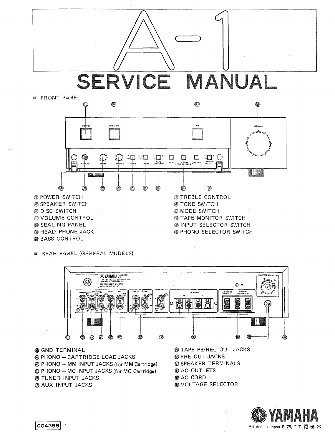
FRONT
PANEL
POWER SWITCH
~
SPEAl<ER SWITCH
@ DISC SWITCH
I®
VOLUME
0
SEALING
0
HEAD
@ BASS
ill REAR PANEL (GENERAL MODELS)
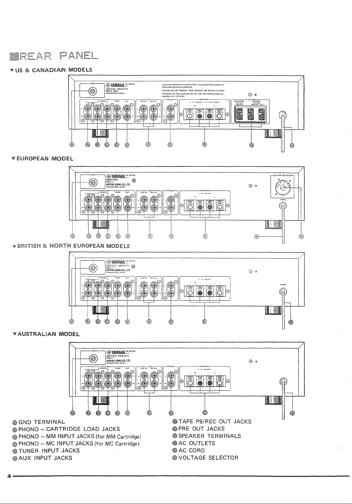
0 GNO
@ PHONO - CARTRIDGE LOAD JACKS
18)
PHONO - MM INPUT JACKS (for MM Cartridge)
6 PHONO -
CONTROL
PANEL
PHONE JACK
CONTROL
TERMINAL
MC
INPUT JACKS (for MC Cartridge)
0 TUNER INPUT JACKS
0
AUX
INPUT
JACKS
TREBLE
TONE SWITCH
~
MOOE SWITCH
@TAPE
<tJli)
INPUT SELECTOR SWITCH
@ PHONO SELECTOR SWITCH
@TAPE
@)
PRE
0 SPEAKER
@AC
@AC
@VOLTAGE
CONTROL
MONITOR SWITCH
PB/REC OUT JACKS
OUT JACKS
TERMINALS
OUTLETS
CORD
SELECTOR
Printed
YA
in
Japan
AHA
5.
78, T. T
r:I
Ii/!)
2K
Page 2

C T
PACKAGE
SPECIFICATIONS
REAR
INTERNAL
DISASSEMBLY
CIRCUIT
BLOCK
ADJUSTMENT
WIRING
PRINTED
SCHEMATIC
PARTS
· · · · · · · · · · · · · · · · · · · · · · · · · · · · · · · · · · · · · · · · · · · · · · · · · · · · · · · · · · · · · · · · · · · 2
PANELS
VIEW
PROCEDURES
DESCRIPTIONS
DIAGRAM/LEVEL
..........................................
CIRCUIT
DIAGRAM
LIST
..
p
· · · · · · · · · · · · · · · · · · · · · · · · · · · · · · · · · · · · · · · · · · · · · · · · · · · · · · · ·
· · · · · · · · · · · · · . · . · ·
· · . · ·
...............
....................
.........................................................
DIAGRAM
................................................................
BOARDS
· ·
.... · ...............
......................................................
..
· · · · · · · · · · · · · · · · · · · · · · · · · · , · · · · · · · · . . . . . . . . . 4
·
... · ·.
. . . . . . . . . . . . . . . . . . . . . . . . . . . . . . . . . . . . . . . . . . . . . . . . 9
·
.... · ..
· · · · · · · · · · · · · · · · · . ·
· · ·
..
·. · .........................
:
..........................
· · · ·
..
· · . · · . · ·
....................
.. · ..
·,....
· · . . . . . . . . . 5
10
11
12
17
3
6
8
Page 3
(SPECIF/CATIONS
SUBJECT
CHANGE
WITHOUT
NOTICE.)
POWER OUTPUT
DAMPING
PRE
INPUT
PHONO
TOTAL
INTER
FACTOR
OUT
SENSITIVITY
MAXIMUM
HARMONIC
MODULATION
SIGNAL/NOISE
RESIDUAL
FREQUENCY
TONE
CHANNEL
POWER BAND WIDTH
N.D.C.R
HEAD
SPEAKER
AC
OUTLETS
POWER SOURCE
DIMENSIONS
NOISE
----------
RESPONCE
CONTROL
SEPARATION
PHONE
TERMINALS
WEIGHT
ACCESORRYS
an
4n
an
an
OUTPUT
IMPEDANCE
/IMPEDANCE
TUNER,
PHONO MM
PH
INPUT
PHONO
PH
DISTORTION
TUNER +
PH
PHONO
DISTORTION TUNER +
------PH-O-NO~M---C~(A------c-cN-=E=T-W--=-o-R~-K-,--)--70-,---d.,--B
PHONO MM (A NETWORK) 85d8
TUN }
AUX
TAPE
------·-·----···---
TAPE TONE
DISC
·---------------
TONE OFF J
TUN I
AUX
TAPE
RIAA
TUNER +
PHONO MM +
PHONO
an,
PHONO MM +
SWITCHED x 2
UNSWITCHED x 1
US
General Model
European Model
North European Model
British & Australian Models
0.02%
0.05%
LEVEL/
AUX,
TAPE
ONO
MC
MM
ONO
MC
SP
OUT
ONO MM +
MC
SP
+ R
OUT
REC
E_C_O_U_T
TONE OFF
ON
f
------------------
\
SP
OUT
DEVIATION
SP
OUT
SP
MC + SP
35W, 0.03%
SP
& Canadian Models
OUT
ON
(8rl)
OUT
OUT
OUT
70W + 70W, (20 - 20KHz)
80W + 80W, (20 - 20KHz)
85W + 85W, (DIN)
100
(1
KHz)
2V/600n
200mV/47Kn
2.5mV/47Kn
60µV
/1
(200pF)
on
230mV (0.01%, 1 KHz)
6mV
(0.01
%,
1 KHz)
Less
than 0.01%,
Less
than 0.005%,
___
L_e_ss_t_h_an_0._0_1
Less
than 0.003%,
35W, 60Hz : 7KHz = 4 : 1
___________
°_Ya~,
112d8
105d8
--
--
-------------·----
Less
than 50µV
TONE OFF
10Hz±0
(
1 00KHz 0 +
20-
TONE
10Hz - 4 ± 0.5dB
ON
[
100KHz o::'::gds
20-
20-
20KHz 0
BASS
±0.2d8
:20Hz±10dB
(TURN OVER
TREBLE
:20KHz±10dB
(TURN OVER
70dB
(1
KHz,5.1
75dB
(1
KHz,5.1
75dB
(1
l<Hz,PHONO short)
10-
50KHz
6mW - 70W
(0.1%
A NETWORK
39mW (Brl)
4n-16rl
100W,
(MAX
TOTAL)
100W
(MAX)
120V, AC60Hz
110/120/130/220/230/240V, AC50/60Hz
110/120/130/220/230/240V, AC50Hz
220V, AC50Hz
240V, AC50Hz
435
(W)
x 117 (H) x
15.8
kg
(34
lb
13
CARTRIDE
COAD PLUG
PHONO SHORT PLUG x 2
8rl,
20-
20KHz, (35W)
20
- 20KHz, (8V)
2_0_-_2_0_K_H----'z,_(_2V-----'----)
__
(8rl)
_
~dB
20KHz'-gdB
20KHz::'::~dB
FREQ+
FREQ+
350Hz)
3.5KHz)
Krl)
Krl)
VOL
-30dB
VOL
-30dB
VOL
-20dB)
381
(D)
oz)
(47Krl
(68Kn
x 2)
x 2)
------------------------------------------3
Page 4
..,
US & CANADIAN
..,
EUROPEAN
,v
BRITISH & NORTH
MODELS
MODEL
L
=
@YAMAHA,',~""'
la:'IVO.TS
-
EUROPEAN MODELS
@VA!DHz
t;AMAMAlS\JJAPAN
29JWATT5
W AR~lr..G-
liJ
PA!:VENT
AFA.1MCETQRAlNCflM;)Sll.lRE
C:.UllCJ'l·OO
ArTO",fflD'l·t.E
0ESSO.JS0El"APPAfi8l
m•E
NJT
PENIJVF.
PAS
Hl.E\IER
CA 9-+0CI( HII.ZAA0,00
TI-tCSE
5Cl'1EWS. SE= HOrT0-,1 C-'Unor,1
ll:5
\115.
llAE
lE5
I
{ffi:i
t<.Or
0<R:!Sc
1!\SWUCTICt-6 AU·
TH:S
© •
© •
v
AUSTRALIAN
@GND
@ PHO NO -
@PHONG
TERMINAL
CARTRIDGE
- MM
e PHONO - MC
@lj)TUNER
f@AUX
INPUT
INPUT
MODEL
INPUT
INPUT
JACKS
JACKS
"
LOAD
JACKS
JACKS (for MM Cartridge)
JACKS (for
MC
Cartridge)
@TAPE
(ID
@)SPEAKER
llm)
@AC
PB/REC
OUT
PRE OUT JACKS
TERMINALS
AC
OUTLETS
CORD
JACKS
\\lf.lVOLTAGE SELECTOR
© •
© •
4--------------------------------------------
Page 5
TTOP
VIEW
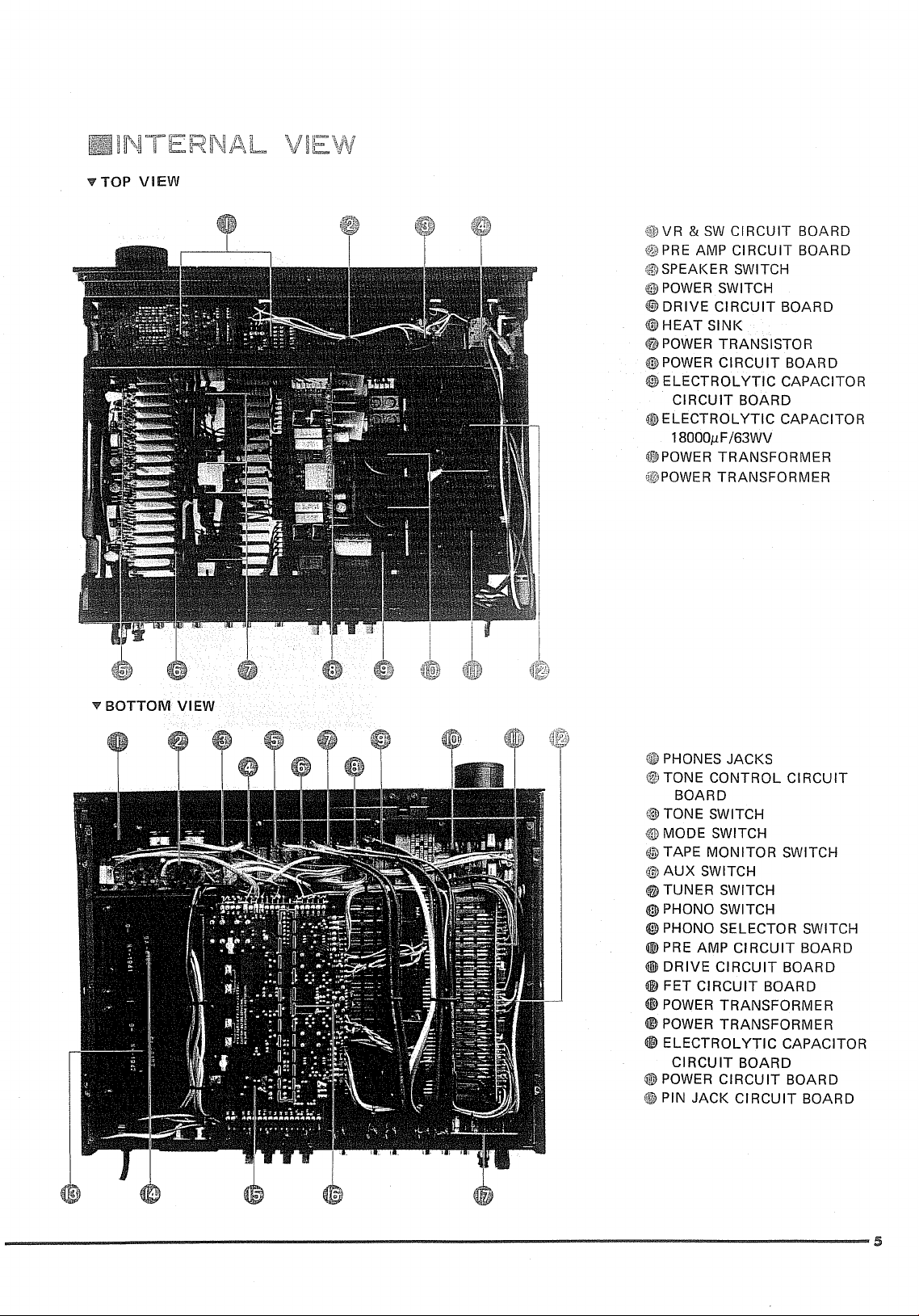
VR &
SW
CIRCUIT
PRE
AMP
CIRCUIT
q[l)
SPEAKER SWITCH
~
POWER SWITCH
DRIVE
{@HEAT
CIRCUIT
SINK
BOARD
BOARD
BOARD
@POWER TRANSISTOR
@POWER
@,
ELECTROLYTIC
®ELECTROLYTIC
@POWER
,jfi\)POWER
CIRCUIT
CIRCUIT
18000µ F
/63WV
TRANSFORMER
TRANSFORMER
BOARD
CAPACITOR
BOARD
CAPACITOR
v
BOTTOM
VIEW
$ PHONES JACKS
@)TONE
CONTROL
CIRCUIT
BOARD
@)
TONE SWITCH
~
MODE SWITCH
@TAPE
@J
@TUNER
~
@l
@PREAMP
@
ill)
® POWER
~
®
~
,;!it)
AUX
MONITOR
SWITCH
SWITCH
SWITCH
PHONO SWITCH
PHONO SELECTOR SWITCH
DRIVE
FET
CIRCUIT
CIRCUIT
CIRCUIT
BOARD
BOARD
BOARD
TRANSFORMER
POWER
ELECTROLYTIC
POWER
PIN
TRANSFORMER
CIRCUIT
CIRCUIT
JACK
CAPACITOR
BOARD
BOARD
CIRCUIT
BOARD
Page 6
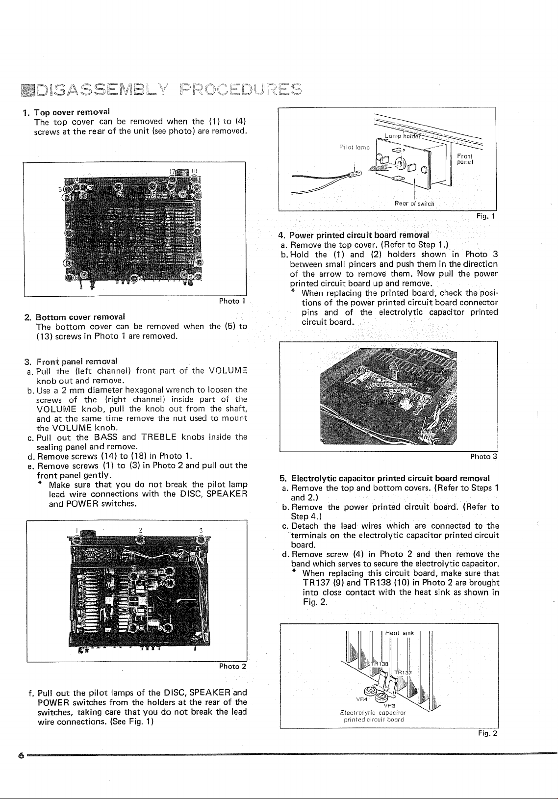
1.
Top
cover removal
The
top
cover
screws
2.
Bottom
The
bottom
(13)
screws in
3.
Front
a.
Pull
knob
b.
Use
a 2
screws
VOLUME
and
at
the
VOLUME
c. Pull
sealing panel
at
cover removal
panel removal
the
out
mm
of
the
out
can be removed when the (1)
the
rear
cover
Photo
(left channel) front part
and
remove.
diameter
the
knob,
same
knob.
the
BASS and TREBLE knobs inside the
and
d. Remove screws (14)
e. Remove screws (1)
front
panel
* Make sure
lead wire
gently.
that
connections
and POWER switches.
to
of
the
can
unit
(see
photo)
are removed.
be
removed when the (5)
(4)
to
1 are removed.
of
the VOLUME
hexagonal wrench
to
loosen
the
(right channel) inside part of the
pull the knob
time remove the
out
from the shaft,
nut
used
to
mount
remove.
to
(18)
in
to
you
(3)
Photo 1.
in
Photo 2 and pull
do
not
break the pilot lamp
with
the
out
the
DISC, SPEAKER
~~-~~;===.·····.h.oic1e,·.~--:·-~-=-
Pi
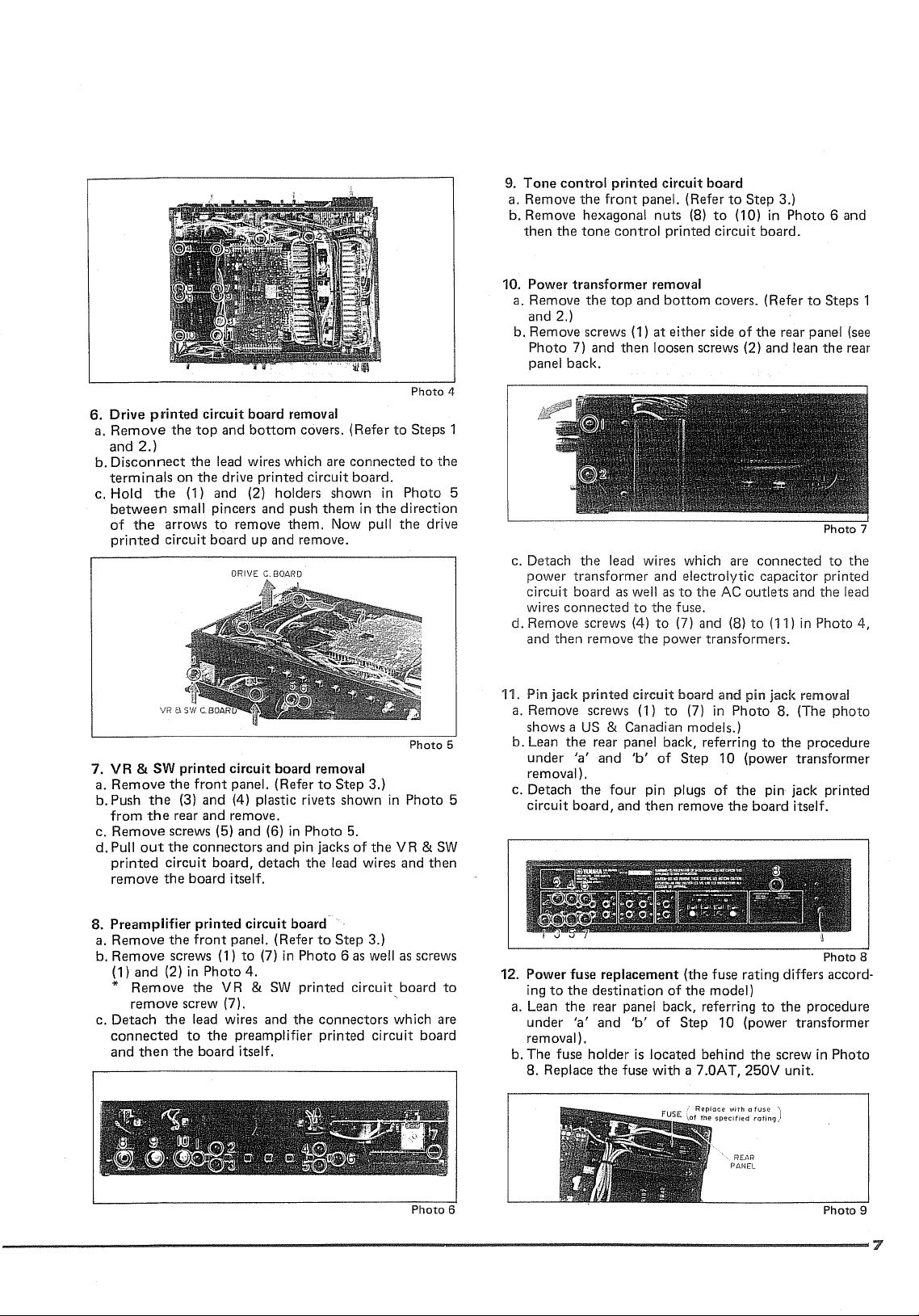
4. Power printed circuit board removal
a. Remove
the
top
b. Hold the (1) and (2) holders shown
between small pincers and push them
of
the
arrow
to
~~~o
lol
lomp
cover. (Refer
~, · ...•
1 I Front
...•
(n;llrr=i
~-i:!.))IL--10
~I
Rear
to
I
I
of
switch
Step
remove them. Now pull
1.)
in
panel
in
the
direction
the
Fig. 1
Photo 3
power
printed circuit board up and remove.
* When replacing
tions
of
pins and of
the
the
power printed circuit board connector
printed board, check
the
electrolytic capacitor printed
the
posi-
circuit board.
5. Electrolytic capacitor printed circuit board removal
a.
Remove
the
top
and
bottom
covers. (Refer
to
Steps 1
and 2.)
b. Remove
Step
c. Detach
terminals on
4.)
the
power printed circuit board. (Refer
the
lead wires which are connected
the
electrolytic capacitor printed circuit
to
board.
d. Remove screw (4)
band which serves
in
Photo 2 and then remove
to
secure
the
electrolytic capacitor.
* When replacing this circuit board, make sure
TR137
into close
Fig. 2.
(9) and
contact
TR138
(10)
in
with the heat sink
Photo 2 are brought
as
shown
to
the
the
that
in
f. Pull
out
the
pilot
lamps of the DISC, SPEAKER and
POWER switches from
switches, taking care
wire connections. (See Fig.
the
that
holders
you
1)
do
at
not
the
break
rear
the
of
the
lead
Page 7
9.
Tone control printed circuit board
a. Remove
b. Remove hexagonal
then
the
the
tone
front
control
panel. (Refer
nuts
(8)
printed
to
to
(10) in
circuit
Step
board.
3.)
Photo
6 and
6.
Drive printed circuit board
a.
Remove
and
b.
Disconnect
terminals
c.
Hold
between
of
printed
7.
VR
a.
Remove
b. Push
from
c.
Remove
d.
Pull
printed
remove
the
top
and
bottom
2.)
the
lead wires which are
on
the
drive
the
(1) and (2) holders
printed
small pincers and push
the
arrows
circuit
& SW printed circuit board removal
the
the
out
circuit
the
to
board
the
front
(3)
and
rear
and
screws (5)
the
connectors
board,
board
remove
up
DRIVE
panel. (Refer
(4) plastic rivets
remove.
and
detach
itself.
removal
covers. ( Refer
circuit
shown
them
them.
Now pull
remove.
G.
and
BOARD
to
(6)
in
Photo
and pin jacks
the
lead wires and
connected
board.
in
the
Step
3.)
shown
5.
of
the
to
in
Photo
direction
the
Photo
in
Photo
VR &
Photo
Steps
to
drive
then
the
5
SW
10. Power transformer
a. Remove
the
top
removal
and
bottom
covers. (Refer
to
Steps 1
and 2.)
b. Remove screws ( 1)
Photo
7) and
panel
back.
4
at
either
side
then
loosen screws (2) and lean
of
the
rear panel (see
the
rear
1
5
c. Detach
power
circuit
wires
d.
Remove screws (4)
and
11. Pin
a. Remove screws (1)
shows a
b.
Lean
under
the
lead wires which are
transformer
board
connected
and electrolytic
as well
as
to
the
to
then
jack
the
remove
printed
US
'a'
the
power
circuit
& Canadian models.)
rear panel back, referring
and
'b'
of
to
the
fuse.
(7) and (8)
transformers.
board
to
(7)
Step
AC
and
in
10
connected
capacitor
outlets
to
pin
Photo
(power
(11)
jack
to
and
8.
the
to
the
printed
the
lead
in
Photo 4,
removal
(The
photo
procedure
transformer
removal).
5
c. Detach
circuit
the
board,
four
and
pin plugs
then
remove
of
the
pin jack printed
the
board
itself.
8. Preamplifier printed circuit board
a.
Remove
b.
Remove
(1)
*
c.
Detach
connected
and
the
screws (1)
and
(2)
Remove
remove
the
then
the
front
in
the
Photo
panel. (Refer
to
(7)
4.
VR &
in
SW
to
Step
Photo 6 as
printed
circuit
3.)
well as screws
screw (7). ·
lead wires and
to
the
preamplifier
board
itself.
the
connectors
printed
circuit
board
to
which are
board
Photo
12. Power
a. Lean
ing
to
under
fuse
replacement (the fuse rating differs accord·
the
destination
the
rear panel back, referring
'a'
and
'b'
of
of
the
Step
model)
10
removal).
b.
The
fuse
holder
is
8. Replace
6
the
fuse
with a 7.0AT,
located
behind
-------------------------------------------7
to
(power
the
screw in
250V
Photo
the
procedure
transformer
unit.
Photo
8
Photo
9
Page 8
CIR
MC
head
The
MC
configuration
circuit
transistors
serve
to
Principle behind noise reduction with parallel connection
It
is
assumed
e2,
have
the
resistors
the
output
e0=e1 x R2/R1 + R2+e2x
U!T
amplifier circuit
head
amp
which
inside
the
are
connected
effectively
that
internal
and
signal
voltage
DESCR!PTIO
I ifier
circuit
is
C-2's -head
reduce
the
two
resistances
e0
will
used
similar
to
amplifier
in
complementary
the
noise
signal
R 1
sources
are
be:
that
sources
and
R1/R1 + R2}
in
the
A-1
of
the
IC. Low-noise
in Fig. 1,
R2,
respectively.
parallel
components.
connected
features
equivalent
and
e1
and
in
parallel,
...
1
r
Fig. 1
In
the
same
way,
the
a
If
vectors
Fig. 2,
way,
two
Based on
following
noise
(N}
In
parallel
3dB
there
accompanies
the
overall noise
Contrary
direct
source
number
signal
*
*
*
will join
the
the
noise
of
the
is
reduced
connected
dB=
10 log10N (2)
the
case
connection
(theoretical
are
current.
to
proportion
resistance,
of
source
Voltage
sistance)
Current
tion
to
Thermal
which
increases in
the
signal
noise
same
this
formula
of
the
two
the
It
components.
the
parallel
resistance.
noise
noise
the
signal
noise
source
second
at a 90°
components
can
be
amplifiers
approach,
between
(dB}
and
in
parallel:
A-1
's MC
brings
value}.
types
of
voltage
is
therefore
voltage noise,
to
and
connections
(noise
(noise
source
of
the
resistance.
part
angle. This
considered
the
so
proportion
will be 1
are
connected
it
is
the
the
number
head
about
However,
noise
in
and
the
necessary
thermal
it
is
necessary
unrelated
which
increases in
resistance}
signal
will be 1
reduced
possible
degree
amplifier,
a noise
as
an
amplifier:
other
the
current
noise
which
to
the
source
to
the
/2e2
means
/y'2
by
in parallel.
to
come
by
of
amplifier
the
reduction
shown
that
accompanies
to
subtract
of
to
determine
agrees
signal
direct
resistance
square
and
that,
as
e0.
In
3dB
when
to
which
stages
two-stage
in
Fig.
one
that
noise
is
the
signal
with
source
propor-
(noise
root
the
in
this
the
the
of
3,
the
in
the
the
re-
of
If
e1
is
then
phase,
no
If
will have
ponents
the
each
remaining
Considered
between
conceivably
the
equivalent
e0 = e1 = e2,
the
same
the
and
noise
amplifier,
the
first
part
two
voltage
two
so
components
unchanged
from
output
the
e1 x R2/R1 + R2 = 1/2e1
and
signals
e0.
amplifiers
same
the
value
at
times
total
two
signals will be
an
average
of
the
to
phase
right
e2
and
when
e1
are
canceled
are
with
of
e0
will
configure
being
in
the
same
perspective,
of
90°.
half
of
90°
if
R1
is
and
e2
out
connected
respect
will
not
canceled
·:
separate
phase.
the
neither
From
formula
R1 = R2
equivalent
have
the
and
there
in parallel,
to
the
signal
change.
th
However,
signals in
out,
and
phase
difference
0°
or
is
observation,
(1) will be:
to
R2,
opposite
will be
they
com-
at
times
180°
but
Signal source resistance
Fig. 3
Fig. 2
Page 9
L
C
DIAGRAfJl/LEV
DiA
R
J
ST
BEFORE MEASUREMENT
•
After
the power switch
• Connect
@
VOLUME
dummy
load resistance (7aW)
CONTROL +
is
push
on, wait 3 - 4 minutes before measuring,
to
the speaker terminals.
MIN
to
be
sure
of
the most stable operation.
MC
AMP
MC~
PHONO
&,
......-
MC!
MM(i::»-----::;;--0"°
CARTRIGE
LOAD
TUNER(Ol-------,---------'--0...-0---,---<o,,_
AUX(OJ~---~--;------'A~U~X~
II~
MC
RELAY
AMP
TAPE
PB
(OJ-------,,---------'
{dBml
+40
+30
+20
+10
a
PHONO
I
I
I
-PHONO
AUX
MM (!kHz)
MC
(I kHz)
-JO
-20
-30
-40
-50
-60
-70
1-81.91
-90
EO
I
I
I
I
I
I
I
I
I
I
I
I
I
I
I
:;
I
I
I
I
I
I
I
I
AMP
PHONO
I
TUNER
I
I
INPUT
SELECTOR
EQ
AMP
1,r-------------
ON
VOLUME
;,-~---------a_
TC.AMP
w
ON
o.
...
"'
TONE
CONTROL
I
I
I
I
I I
I
I
TONE
I
I
I
I
MAX
I\
\
~IOdB
VOLUME
I
I
I
I
I
I
'
CONTROL
+IOnB
I
I
I
I
I I
I
I
I
I
I
I
I
I
I
I I
I
I
I
I
I
I
DISC
-----
>
STEP
2
.
POWER
EQALIZER
DC
MC
I ,
I ,
I ,
1,'
ON
~'
MAIN
AMP
'I
PHONES
'
Distortion
3
Suplly Voltage
AMP
Offset Voltage
AMP
POWER
P.C.B
PRE AMP P.L.B
VR4a1
VR4a2
VR &
VR3a1
VR3a2
(L
(R
SW
(L
(R
CH)
CH)
P.C.B
CH)
CH)
Digital Multi
Meter
Digital Multi
Meter
Audio Frequency
Generator (2aKHz,
2aKHz
>TERMINALS/
TEST
POINT
POWER
PRE AMP
TP1
TP2
REC
(L
(R
OUT
R.C.B
P.C.B
CH)
CH)
JACK
3V)
PATING
OR
STANDARD
+35 ±
1V
-35 ± -a.5V
av±
2aamv
Distortion+
RE-
MARKS
Fig. 1
Fig. 2
Min
Fig. 3
Distortion ratio
CH)
P.C.B
CH)
Meter
Digital
Multi
Meter
Digital Multi
Meter
DRIVE
TP1, TP2
TP2, TP4
P.C.B
(LCH)
(R
CH)
Electrolytic
Capacitor P.C.B
TP1, TP3 (L CH)
TP2, TP4
(R
CH)
OIUlf/\L
/v\LJLTl/vlETEn
<lil
POWER
·-35
:_
IV
av±
7.4 ±
VOLTAGE
---35 '.::O.SV
10mv
Fig. 4
2mV
Fig. 5
----··
RELAY
.. · DRIVE
4
DC
POWER
lndring Current
5
MAIN
AMP
I
I
I
I
I
I
I
I
I
I
I
I
I
I
I
I
I
I
I
I
I
I
I
I
I
I
I
I
I
I
I
REC
OUT
I
CIRCUIT
Offset Voltage
AMP
DIGITAi_
MULTIMETER
19
DC
offset
OV
· IOmV
Audio frequeucy
Generator (
201<.Hz
[ill§]0
o
a~
eaiDDDee
DOD
Fig3
DRIVE
P.C.B
VR5a1 (L CH)
VR5a2
(R
Electrolytic
Capacitor
VR1a1 (L CH)
VR1a2
)
(R
--------------------------------------------10
Page 10
PIN
JACI(
CIRCUIT BOARD
1.
PINJACK
VR
S.
SW
CIRCUIT
BOARD
(21
NA07044
NA07136:US
GA61890
-------.,
VI r
I
I
I
WH,
BR
I
OR I
AC
WHI
OR
8.5V
3BV
0
38.2V
6.5V
38V
I
I
I
I BE
I
I
I
I
I VI
I RE
I
I
I
I
HL E
HR
BE
WH
WH
OR
OR
VI
RE
BL
BE
WH
VI
OR
OR
BL
BL
ns-35tR
NA07044
NA07136:
US
MOOEL
E
RE
ELECTROLYTIC
CAPACITOR
CIRCUIT
NA07130
NA07 I 29:
BOARD
US MODEL
>12
>12
MODEL
L.~-3,~_J
GY
L----------------~
'-----------------~
GY
E RI
0
a::
.J
w
0
0
"'
OJ
0
::E
f-
a
~
a::~:...:
U
Otf>
w
br::
>
,::{,::{
zz
2.
FET
CIRCUIT
CIRCUIT
BOARD
BOARD
NA07042
NA07046
UNSWITCHED SWITCHED
•WIRE
BL
BR
RE
OR
YE
GR
II>
BE
Pio-
S,.
II>
Ii>
Ii>
II>
COLOR ABBREVIATIONS
Black
Brown
Red
Orange
Yellow
Green PK
VI
GY
WH
GG
SB
Pio-
Ii>
!lo-
Ii>
11>
Ii>
Violet
Gray
White
Grass Green
Sky Blue
Pink
Blue
NA07133:
NA07132:
NA7176
NA7134
NA0704
CANADIAN MODEL
US
MODEL
· EUROPIAN a BRITISH MODELS
. EUROPIAN, SEC MODEL
I : GENERAL a
3.
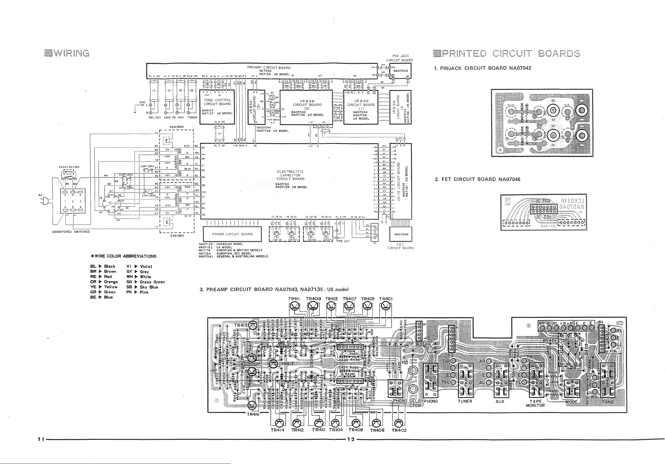
PREAMP
AUSTRALIAN
CIRCUIT
MODELS
BOARD NA07043,
TR411
NA07135:
TR409
US
TR403
model
TR407
TR405
SP
TR40I
FET
CIRCUIT BOt\RD
11
----------------;..,_--------------------------12
TR4I4
TR4I2
T R4I0 T Fl404
TR408
TR406
TR402
---------------------------------------------
Page 11
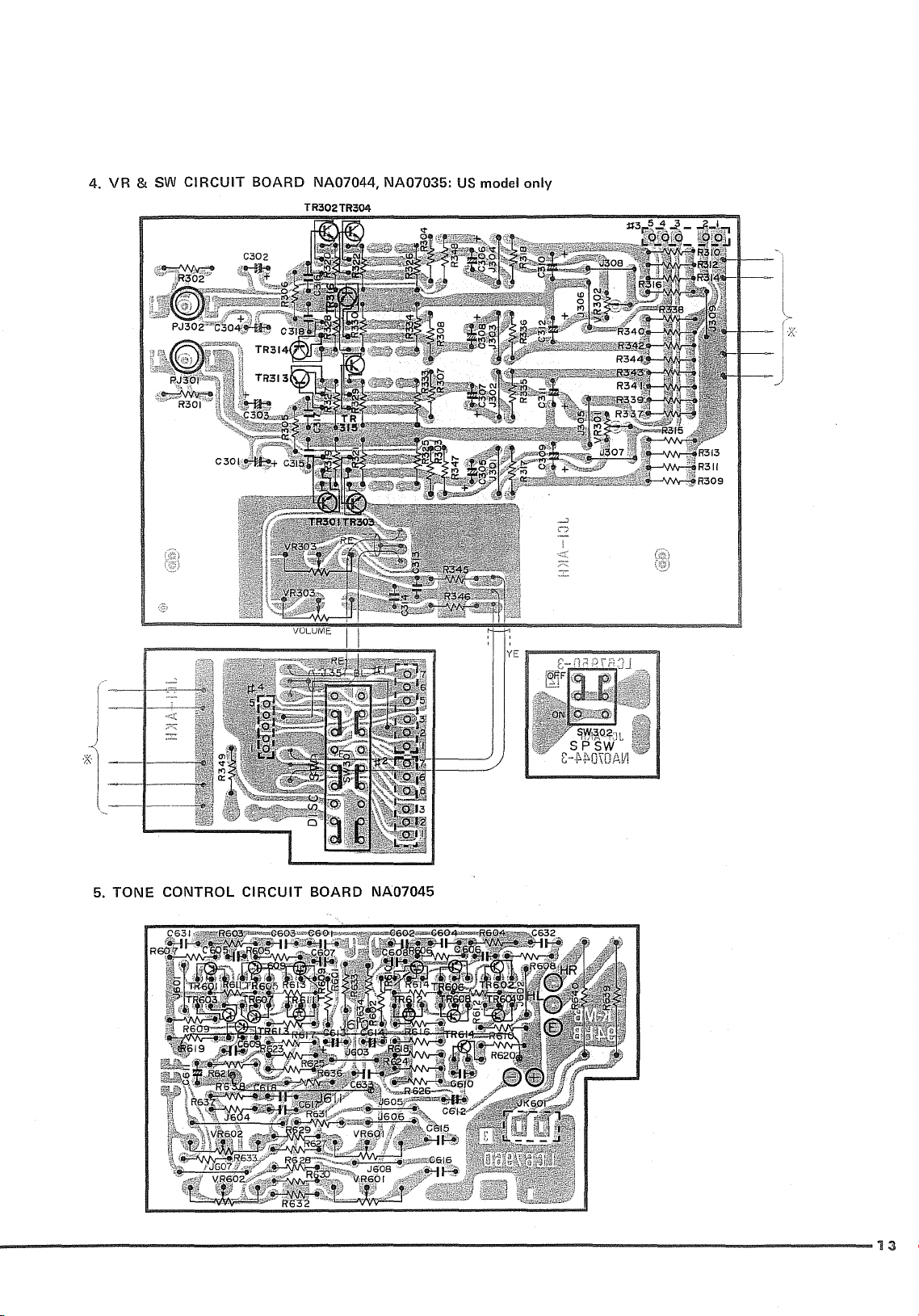
4.
VR
&
SW
CIRCUIT
---------
BOARD
NA07044,
TR302TR304
-----------------:----
NA07035:
US
model
only
5.
TONE
CONTROL
CIRCUIT
BOARD
NA07045
Page 12

6.
DRIVE
CIRCUllT
BOARD
NA07040,
NA07031:
US
model
only
(0
14-----------------------------------------------
Page 13

7.
ELECTROLYTIC
CAPACITOR
CIRCUIT
BOARD NA07130, NA07129:
US
model
only
8.
POWER
l---i--F202,
L---
CIRCUIT
1
BOARD NA07041:
NA07133:
NA07176: EUROPEAN model
TO
ELECTROLYTIC
CIRCUIT
203:
GENERAL,
BRITISH
AUSTRALIAN,
models
GENERAL
CANADIAN
CAPACITOR
BOARD
models,
NA07132:
US
model
model, NA07134: EUROPEAN,
MODELS
EUROPEAN,
GENERAL
AUSTRALIAN
US &
EUROPEAN,
BRITISH,
PC
model
CANADIAN
ESPEC
F201,202,203
1.0A/125V
1A/250V
800mA/250V
Page 14

-
I
Page 15

Exproded
view
\
0
(s
-2-
Page 16

Parts
List
Ref.
No.
32joo!oo!AA!o9!3o
1
*
*
*
*
*
*
*
*
*
*
*
*
*
*
*
*
*
*
*
42jooioo!
2
42:00
:00
42!00:00!
32: oo!oo: MZ[
42100:00:
3
42:oo!ooi
42:00:00:
4
42[00!00:
5
42:00:00[
6
32;00:00:NB
7
32:00:00!
8
42[ooioo[
9
42iOO:OOi
10
32:00:00iAA:09:31
11
32:00!00:AAi09[31
32:00!00:AAj09:31
32:00:00!AA:09:31 :30
32:00:00!AA;09:31 [40
32:00[00:AA:09:31
42[00[00[ LB:20[12:10
12
42:00:00!
42jOO!OO:
42:oo:oo: LA!00:23110
13
42[00:00:
14
42100;00: LB:40:03:90
15
42:00:00! LB!10:01
16
32:00:00i
17
32:00:00[ NBiOBiB0:30
18
32!oo!oo[
42[00!00[ EN!o3[00[20
19
32[00:00[ BA[o1!22
20
32iOO!OO!
21
42:00!00:
22
32:00!00[AA:09j07
23
32:00:00: BA:07:34:70
24
25 42:00:00! EA:23!00
32:00:00i
26
42!00:00: EV!10!20:3o
27
32:00[00: NB[08157
28
29
32JOO
[00 AA:09
32:00:00
30
31
32
33
34
35
36
37
* New parts
, I I 1 I
42j00[00
32:00:00 CBl07!45:10
! I I , ,
32:00iOO CB:06:BBiSO
32:00:00
32[00100 CB:OB:36:40
32:00;00
32[00[00 BAjo1[34!20
'
'
'
i
'
i
i
'
i
'
Part No.
MG;oojo3
i MGi00:04
MG:00[08
omsj90
CB
j07i27
CB
:OB:86
LB
!B0!18 iso
EN[33[00[10
ED:33!00;60
[08[14[80
CB
:07[81 !70
LA[oo:02:so
EV! 10:33 ioo
LB
[20:13
LB
:20:14
LB
:20:11 i40
NA!07;04 i20
NB[OB:60
CB
:08:68
El
:23j00[80
CB
[08[69
NB:07:94;90
ENi03\00!20
AA[OBj99
cBioa:69[10
'
!
'
'
'
Description
Topcover
!so
SF
AC
Cord
-do.-
jBO
-do.AC Cord Ass'y
Cord Stopper SR-4N-4 B
j50
-do.-
AC Socket
Bind
Head
Tapping Screw M3 x 8
Bind
Head
Screw M3 x 6
Terminal Ass'y
Saucer
Earth
Lug
Hexagonoral
Rear
:DO
-do.-
:10
-do.-
f20
-do.-
-do.-
-do.-
!50
Fuse
-do.-
:OD
-do.-
[70
Speaker Terminal
Pin-Jack
-do.Short plug
;80
Pin.Jack
Panel
-do.-
:40
Bind
Knob, Tone Control
:80
Push
[90
Bind
:10
Hexagonal
Screw
Pan
[60
Shaft
[00
Hexagonal
Knob Ass'y
[90
Bottom Cover
:90
Leg
Bind
Push
Plastic Rivet
Spring
:BO
Push
Shaft Holder
Rolling
'
I
Nut
Panel
Holder
(4P)
(2P)
(4P)
C.
Board
Unit
Head
Tapping Screw M3 x 8 ZMC2-Y
Button
Head
Tapping Screw M3 x 8
Nut
Head
Screw M3 x 6 FCrM3-3g
for
Rolling
Panel
Nut
Ass'y
Head
Tapping Screw M3 x 8
Button Frame
for
Push
Botton
Button
Panel
!30
'
'
: i
!40
!50
i30
105°C
VM0077
type A4, 7.5A 240V
SR-3P-4
3mm
M3
M5
#7347
M3
BA
FCM3-BL
FCM3-BL
FCM3-BL
FCM3-BL
FCrM3-3g
FCrM3-3g
ZMC2-Y
Markets
R,U,C
E,G
A
B
R,U,A,E,G,C
R,U,C
R
u,c
A
E
G
B
R
U,A,C
E,
G,
B
R,A,E,C,B
u
Remarks
-3-
Page 17

Exproded
view
-4-
Page 18

•Parts
Ref.
No.
42·!00 ioo!GA[61
1
*
*
*
*
*
*
*
*
*
*
*
*
*
*
*
*
*
42ioo!oo!GAJ61 las
42!00
42
ioo ioo !
42ioo!ooiGA!61
2
42:00
42iooioo!GAi61
42[00;00:GA[61
42:oo
3
42:ooioo:
4
'
5 32iOO!Ooj NAi07:04 :10
32:00:00: NA:07:13 :20
32:00!00[ NA:07:13 i30
32:00iOOi NA:07[13 :40
42!00;00; KB!oo:01
F201
F202 42:00!00! KB:00:10 !60
F203 42:00:00! KB:00:07
32:00!00:
6
'
7 32;00!00:NA/01:12 :90
32!00
42:00!00iFZ:00:11
C115
C116 42:00:00! FZ:00!11 i80
Tr135
42:00:00!
Tr136
42:00:00!
42;00:00: EN!03:00[20
8
9
32:00:00[ BA:06;27 ;60
10
42[00!00[
11
42[00[00[
12 42)00:00!
13
42j00[00:
14
42:00!00i
42:00:00! EA:34j08 :70
15
16 42:00:00!
!
17
32:00 ioo: NA!07
32!oo:ooiNA!07:13
18 42!00:00: KA:80:04 :90
19 42:00:00: FZ :00:09
'
20
32!oojoo! NA[o1[04 !4o
32:00iOO: NA:07[13 j60
SW301
42:00iOO! KA[B0:04:70
SW302
42:00:00[ KA[B0!04:80
42[00
VR303
32!00
'
21
32i00!00!NAj07j13
32:00!00!NA:07:14 :70
JK601
42:00:00i
VR601
42:00
VR602
42100:00!
List
Part No.
!OOiGAi61
GA
iooiGA:61
!oo[
EN
EZ !00[03
'
'
'
CB
'
:
!OO:
NA!07
iA
iA
LBj30i04:90
iL
iA
EZ:33:01 [60
iC:11j16j10
LA
I
I
'
'
'
OOjHY!00:06 i50
OOi
BB
i
LB
!OOj
HS
HS
* New parts
!a6
[oo
!oo
:90
!oo
:61
[92
ioo
ia1
ioo
ia9
:oo
i91
ioo
i93
!oo
!33!00
:10
[9o
I
'
'
I
:
;oo
[20
:08:77 !90
I
'
'
[13
:OO
:80
:09:13 ;00
:09!13
:OO
100[02
j30
j07:47 ;10
:00:02 :80
'
'
'
I
'
!04
!OO
:10
;70
I
'
:
'
106:63
:40
I
'
I
:
'
j70
[30[06
[40
[32
:04
!20
!32
!04
:BO
Description
Transformer
-do.-
-do.-
-do.-
-do.-
-do.- -do.-
-do.-
-do.- -do.-
Bind
Head
Tapping Screw M3 x 8 FCM3-BL
Blaze-Washer
Power Supply C. Board
Fuse
-do.-
-do.-
C.
Board Holder
-Electrolytic
Electrolytic
Transistor 2SA913
-do.-
Pan
Head
Radistor
Transistor Socket
Mica
Transistor 2SA747
BW
Head
Transistor 2SC1116
Pan
Head
Earth Lug
Drive C. Board
-do.~
Power Switch 125V 15A
Ceramic
VR & SW
Push
Push
Variable Resistor
Sealed
Tone Control C. Board
Headphone Jack JK601
VR
Bass
VR Treble Control W-10K x 2
Head
-do.-
-do.-
-do.-
Cap.
C.
-do.Cap.
Lug Type
-do.-
Tapping Screw
Base
Screw M3 x
Screw
Cap.
C.
Board
-do.Switch
for
Speaker
Switch
for
Disk
Plate
-do.-
Control
Front
-do.-
-do.-
-do.Rear
-do.-
Screw
M4x8
125V
1.0AT
250V
1A
800mA 250V
Board u
18000µF/63V
-do.-
M3 x 8
16
M4x
87
¢3mm
0.01µF / 150V
A-50K
B30K x 2
ZMC2-Y
ZMC2-Y
FNM3-3m
FCM3-BL
ST-4
Markets
U,C
R,E
G
A,B
U,C
R,E
G
A, B
R,A
u
C
..
E,G,B
R,A
u,c
E,
G,
B
R,A,E,G,C,B
R,A,E,G,C,B
u
R,A,E,G,C,B
u
u
R,
A,
E, G C,
Remarks
B
-5-
Page 19

Ref.
No.
32jooioo l
22
32;ooiooiNAjo1!13
42:00
SW401
42:00;00:
23
42:ooiooiJB
24
42:00:00:
25
42:00:00:
26
Part
No.
NA[07[o4
:oo i KA:80:04
ED:3310060
!00:06!10
CB
:06:88
cBjos[41
Description
Pre
C.
!3o
;5o
!50
:BO
iso
Board
-do.-
Push
Switch
Bind
Head
Screw
Pilot Lamp 14.5V
Plastic Rivet
Lamp
Cap
of
Orange
Color
M3
x 6
FCM3-BL
80mA
R,A,E
u
Markets
G,C,B
Remarks
*New
-6-
parts
Page 20

Ref.
No.
32[ooiooi
5
*
32[00[00[ NA!07[13
32[00:00i NAi07:13
32100:00! NA:07[13:40
42:cioiooi
Tr201
42:ooiooi
Tr202
42iooiooi
Tr203
42\00\ooi iA [08j12[00
Tr204
42:ooiool iD io4l76:0o
Tr205
42iooiooi
Tr206
42:00:ooi
Tr207
42jooiooj
Tr208
42:ooiooi
Tr209
42:ooiooi
Tr210
42:00[00:
Tr'211
Tr212
42:00:0D!
42[00:DD!
Tr213
Tr214
42:00:DD[iA :D6:73j10
42:00:00: iD :05:26
Tr215
42joojoo[
D201
42:DO:DO!
D202
42[00:00 i
D203
D204 42[00:DDliH
D205 42:0D:DD:
42:00:00 [ iF
D206
42:0D!DD! iF
D207
42:DO:OO i iF
D208
42:ooioo i FZ :ooio6
C201
42Jooloo ! FZ [00:06
C202
42[00!00[ Fz!oo[o6
C203
42joo:ooi
C204
42iOO:OOi
C205
42:00:00:
C206
42:00:DOiFJ :17[84:70
C207
42:D0:00:FJ :17[84:70
C208
42:00jOD:FJ :16:74:70
C209
42:00:00:
C210
42!00
C211
42[00
C:212
42:00;00
C213
42:00:00
C214
42!00[00 FMi11
C215
42:00:00
C216
42
C217
C218
R201
R202
R203
R204
R205
R206
R207
R208
:DO
42:00/JO FMj39!31
42!oo!oo HK:15:54:70
42:0000
42\oopo
42:oopo
42:oobo
42:ooioo
42[oopo
42[00:00 HK!15j61
* New parts
Part No.
Power
Supply
C.
NA[o1!04[10
[20
i30
iB
[o5:66[oo Transistor 2SB566
iA
!08:72ioo
iA [08[12:oo
iC
!11[75;00
iC
i 11i15:oo
iA io8:44i10
iC
i 19:18:oo
iC
i 19:13:00
iC
i19j18:00
iC
!12i13i10
iC
:19i18iDD
!30
iH
ioojo2j4D
iH
/00;04:70
iH
:00;02
:40
iDD:04:70
iF
:D0:03;50
:00[05:70
:0Dj07:70
iOD:05:70
:80
:80
[80
FJ
j14:91
po
FJ
:17:84j70
FJ
:17j84j70
FJ
[16!74:70
:oo
i FA
11~11)0 Mylar
1
!OD i FJ
:15
:71
po
FJ
:16:74:70
FJ
!16:74:70
[71
OD
FZ
:ODp4
!70
;OD
FZ
:OD
D2
pO
bD
HKl1566
HKj15~8:20
HK[15~8
HK:1566:80
HKl15:73:30
HK/15:62:20
SD
~O
j50
-do.-
-do.-
-do.-
-do.-
-do.-
-do.-
-do.-
-do.-
-do.-
-do.-
-do.-
-do.-
-do.-
-do.-
-do.-
-do.-
-do.-
Diode
-do.-
-do.-
-do.Zener Diode WZ-130
-do.-
-do.-
-do.-
MM
Cap.
-do.-
-do.- -do.Electrolytic
-do.-
-do.- -do.-
-do.- -do.-
-do.-
-do.-
-do.Cap.
Electrolytic
-do.-
-do.-
Bipolar
Cap.
Electrolytic
-do.-
-do.-
Carbon
Resistor
-do.-
-do.-
-do.- -do.-
-do.-
-do.-
-do.-
-do.-
Board
Cap.
Cap.
Cap.
Description
2SA872
-do.-
-do.2SD476A
2SC1775
-do.2SA844
2SC1918
-do.-
-do.2SC1213A
2SC1918
2SC673A
2SD526
1S1815
10431
1S1815
1
D431
HZ-6C
VD1212
HZ-6C
0.1µF
-do.-
1000µF/
470µF /
-do.47µF
-do.O.OlµF / 50V
1000µF / 25V
47µF / 50V
-do.10µF
10µF / 16V
0.47µF / 50V
100µF / 16V
470.(l
6.8K.(l
8.2Kn.
6.81<.(l
331<.(l
2.2Kn.
1.5Kn.
250V
/
25V
63V
50V
/
/ 50V
MS
MS
MS
z
(I<)
R,A
u
C
E,G
Markets
B
Remarks
-7-
Page 21

*
Ref.
No.
42iooiooi
R209
42ioojool
R211
42:0o:oo!
R212
42!00!00! H
R213
42:ooiooi
R214
42:00:ooi
R215
42:ooioo i H
R216
42[00[00:
R217
42:ooioo[
R218
42:oo!ooi
R219
42ioo:ooi
R220
42[00:00!
R221
42:00:00:
R222
42:00j00i
R223
42:00!00:
VR201
42i00:00:
42:00!00: LB:20109:00
42:00;00!
42:00:00:
42[00!00[
32!00!001
i
i
I
'
'
'
'
'
'
'
'
'
'
!
'
'
'
:
'
'
'
'
'
'
'
'
:
'
'
'
'
:
'
'
'
'
'
I
'
'
'
I
I
*New
parts
Part
No.
HKi15!66!so
HK!
15[71
HKi
15:71
K:15
[s1
HK!
15:81 !so
HK!
16:82:20
Ki
15!71
HK!
15[62[70
HK:
15164:70
HK[
15[76;80
HK/
15[81
HKi
15:73:30
HK:
15:62:20
HK:
15!76:80
HT:41[01
LA
100:20/00
LB:20:10!60
LB:30:01
LBi4o[o4j5o
sAjo6:91
'
:
'
'
I
'
'
'
'
'
' ' '
'
'
'
'
'
'
'
'
'
'
'
'
I
'
!
'
'
'
'
'
'
!
'
'
'
'
'
!
i
'
'
'
'
'
!
'
l
'
'
'
'
Carbon
[oo
!oo
ioo
loo
ioo
:60
:30
i4o
'
;
;
-do.-
-do.-
-do.-
-do.-
-do.-
-do.-
-do.-
-do.-
-do.-
-do.-
-do.-
-do.-
-do.Variable
Wire
Fuse
Connector Socket
Radiator
'
:
;
'
'
'
'
'
'
'
!
'
'
I
Description
Resistor
Resistor
Lapping Terminal
Holder
Pin
PC
-do.- -do.-
-do.-
6.8Kn
10Kn
-do.-
100Kn
180Kn
220Kn
10Kn
2.7Kn
4.7Kn
68Kn
100Kn
33Kn
2.2Kn
68Kn
B2.2Kn
3P
4P
SR-29R
P=
7.5
YSH402P
Markets
R,U,A,C
E,
G,
B
Remarks
-8-
Page 22

Ref.
No.
7
*
Tr133
Tr134
Tr135
Tr136
Tr137
Tr138
D101
D102
D103
D104
C101
C102
C103
C104
C105
C106
C107
C108
C109
C110
C111
C112
C113
C114
C115
C116
*
C117
C118
*
C119
C120
L101
L102
R101
R102 42:00:00
R103 42:00!00jHKj 15153
R104
R105
R106
R109 42:00:00
R110
R111
R112
R113
R114
R115
R116
R117
R118
R119
R120
R121
*New
parts
Part No.
32jOO!OO!NA!07i 12!90
32jOO[OO[NAj07[ 13joo
42:00!00i
42:00:00!
42:oo!ooi
42:00!00:
42:00iOO:
42!00100!
42:00[ooj
42;00!00!
42:00:ooi
42jooiooj
42!
oo!oo! FD! 15:23:30 Polystyrene Cap.
42:00:00:
42:
OOiOO:
42:00:00:
42:00:00!FA: 11:45:60
42:00:00!FA ! 11:45[60
42:00!oo; FA!
42)00jOOjFA ! 11\51
42:00!00! FA/ 11:51
42[00!00jFA:
42100[00:FZ !00:06!80
42jOO!OO:
42:00:00j FZ :00:06;80
42:00:00! FZ !00:06:80
42:00!00: FZ !00[11
42:00!00[ FZ ;00:11
42JOO[OOi
42[00[00 !
42jOOiOO:FMj09:71
42iOO:OO:FM
42:oo;oo
42:00:00:GD:90[00!50
42:00[00
42100100/HKJ 15:53/30
42j00100!HK! 15[58!20
42\00
jOO
42:00jOO
42:00!00!HKj 15[34!70
42!oojoo !HK:15:34:70
42
/00 /00
42iOO!OO
42
iOO
:00
42:00!00 !HM:05:24
42:oojoo iHKj15:72
42100;00
42!00
!OO
42!00[00 HU[62[41[00
42!
ooloo
iC
i19:13[00
iC
:19!13iOO
iA
!09!13ioo
iA
i09i13jOO
iC
[12:13:10
iC
[12j13i10
iH
!OOJ02i10
iH
!00[02120
iF
!00/00:40
iF
ioo:00!40
FD!
15123:30
FD
i 15j23:30
FD
j 15:23\30
11
:51
joo
!DO
iOO
11
:51
jOO
FZ j00j06i80
:80
!BO
FC
[ 12:62:20
FC
i 12162 ;20
:00
:09:71
joo
!GD
:90[00150
!HK
i 15:53
:30
\HK
i 15:53
[30
[30
jH
Ki
15
i58
[20
!HK
j 15
j34
!70
:HK:
15!34j70
jH
M /05 :24
;70
[HMj05 [24:70
!HM
j05
[24
[70
!70
:20
!HK
j15
!72
:20
iHL !62
:41
po
HZ
!00[01[10
Description
Electrolytic
Transistor 2SC1913
-do.-
-do.-
-do.-
-do.-
-do.-
Diode S-5151
-do.-
-do.-
-do.-
Mylar Cap. 0.056µF / 50V
-do.-
-do.-
-do.-
-do.-
-do.-
MM
-do.-
-do.-
-do.Electrolytic Cap.
Metalized Polyester Film Cap.
Bi-Polar Electrolytic Cap.
Coil
-do.-
Carbon Resistor
Cement Molded Resistor
Carbon Resistor
Metal Oxide Resistor
Cap.
C.
Board
-do.-
-do.-
2SA913
-do.-
2SC1213A
-do.-
S-5151R
1S1555
-do.330µF
-do.-
-do.-
-do.-
Cap.
Lug
-do.-
-do.-
-do.- -do.-
-do.-
-do.- -do.-
-do.-
-do.-
-do.- -do.-
-do.-
-do.-
-do.-
-do.-
-do.- -do.-
-do.-
-do.- -do.-
-do.- -do.-
-do.-
-do.-
Type
-do.-
-do.-
-do.-
0.1µF
-do.-
-do.-
-do.-
0.1µF
-do.-
-do.-
-do.-
3µH
-do.330n
-do.-
-do.-
820n
4.7n
-do.-
-do.-
-do.5P
-do.-
22Krl.
2P
-do.1P
-do.-
10n
4.7ri,
500V
/
/ 50V
/ 250V
18000µ F / 63V
-do.-
2.2µF
-do.-
10µF
0.47n
(J)
MS
MS
/ 100V
16V
/
(Kl
(Kl
Markets
u
R,A,E,G,C,B
Remarks
-9-
Page 23

Ref.
No.
R123 42:ooioo!HK:15166:80
R124
R125 42:ooioo:H1<!15:56;8o
R126 42:00:00:HK[
FR
101
FR102 42:00:00\HWi 19146;80
VR101
VR102
RY101 42jOO:oo[ l<Ci 00;05:30
RY102 42/00:00:l<C :00/03[00
Part
No.
42:ooioo:HKi
42!
oo[oo!Hwi
42:0oioo:HT[41[00;20
42:0oiooiHTi41J00:20
42:00:00J LB
42:00!00:
15:66!80
15[56:80
19[46[80
:30:01
LB
:40[04:60
:20
l l ;
: '
I I :
' -
' :
Description
1P
Metal Oxide Resistor
Carbon Resistor
-do.-
-do.-
-do.-
Fuse Resistor
-do.-
4.7n
6.8Kn
-do.-
680fl
-do.-
68fl
-do.-
Variable Resistor B 1 l<fl
-do.- -do.Relay
Read Relay
Connector
-do.-
3P
-do.-
60mA
SV101<R
Markets
Remarks
: '
'
' '
: '
l : I
! l I
: l
' '
'
'
'
I !
' :
'
'
'
l I
'
'
'
' '
*
New
-10-
parts
' '
'
Page 24

*
Ref.
No.
32!
17
Tr501
Tr502
Tr503
Tr504
Tr505
Tr506
Tr507
Tr508
Tr509
Tr510
Tr511
Tr512
Tr513
Tr514
Tr515
Tr516
Tr517
Tr518
Tr519
Tr520
Tr521
Tr522
Tr523
Tr524
Tr525
Tr526
Tr527
Tr528
Tr529
Tr530
Tr531
Tr532
0501
0502
0503
0504
0505
0506
0507
0508
0509
0510
0511
0512
0513
0514
0515
0516
0517
0518
0519
*New
OOiOO[NA\07[04jOO
32! oo!oo!NAjo1! 13j10
42:00IOOi
42100:00!
42\oo!ooi
42/ooioo!
42iOOiOO:
42[00[00:
42:00:00;
42: ooiooi
42/00:ooi
42[00!00;
42:00!00!
42:00:00i
42:00iOOi
42100:00:
42:00!00!
42: 00:00! iA:
42:00:00:
42joo!ooi
42/00!00:
42:00!00[
42!00[00:
42;00:00!iC :12:13;10
42:00:00!
42:00:00[
42:00:00j
42:00:00!
42!00!00;
42! oo!oo!
42Joo:ooi
42iOD:OOi
42!
oo!oo:
42:00:00!
42:ooloo!
42100:00:
42ioo!ooi
42:oo:oo:
42iOO:OOi
42:00:00:
42:00iOO!
42[oojooi
42:00:00!
42:00;00!
42!00!00!
42[00!001 iF
42:00/00[
42:00!00!
' ' '
42:00\00!
42:00:00!
42:oo:ooi
42/00/00/
42100:00:
parts
Part
No.
iC
i17:75jOO
iC
:17[75:00
iC
[17:75ioo
iC
:11:75/oo
iC
[17j75ioo
iC
!17[75[oo
iC
:17!75:00
ic ! 17[75iOO
iA
io8/72ioo
iA
;08!12!00
iA
!06!73!3o
iA
:06:73j30
iA
:o6j73j30
iA
/ 06:73/30
iA
:09:14:50
09:
iA
[09:14!50
iA
io9[14[5o
iC
! 19:53:50
iC
! 19:53:50
iC
;12(13:10
iC
i 12:13:10
iC
l 12:13;10
iA
!09:14i50
iA
:09!14:50
19:53:50
ic
ic
19[53!50
07;34:30
iC
iC
07:34j30
05[61
iA
05j61:70
iA
iF
00!00:40
iF
OOi00:40
iF
00!00:40
iF
00!00:40
iF
00:05:70
00:05:70
iF
iF
00!05:70
iF
00[05[70
00[00[40
iF
iF
00,00!40
iF
00!00:40
00:00;40
iF
00:00/40
iF
00!00:40
iF
00!00[40
iF
00!00:40
iF
00;00!40
iF
00/00:40
iF
00!00;40
Drive
C.
Board
-do.-
Transistor 2SC1775
-do.-
-do.-
-do.- -do.-
-do.-
-do.-
-do.-
-do.-
-do.-
-do.-
-do.-
-do.- -do.-
-do.-
-do.-
-do.-
14[50
' '
-do.-
-do.- -do.-
-do.-
-do.-
-do.-
-do.-
-do.-
-do.- -do.-
-do.-
-do.-
-do.-
-do.-
-do.- -do.-
-do.-
-do.-
[70
-do.-
-do.-
Diode
-do.-
-do.-
-do.Zener Diode
-do.-
-do.-
-do.-
Diode
-do.-
-do.-
-do.-
-do.-
-do.-
-do.-
-do.-
-do.-
-do.-
-do.-
Description
-do.-
-do.-
-do.-
-do.-
-do.-
-do.-
2SA872
-do.-
2SA673A,
-do.-
-do.-
2SA914Q,
-do.-
-do.-
2SC19530,
-do.-
2SC1213A
-do.-
-do.-
2SA9140,
-do.-
2SC19530,
2SC734
-do.-
2SA561
-do.-
1S1555
-do.-
-do.-
-do.HZ6C
-do.-
-do.-
-do.-
1S1555
-do.-
-do.-
-do.-
-do.-
-do.-
-do.-
-do.-
-do.-
-do.-
-do.-
C,
R,
R,
R,
R,
D
S,
S,
T
S, T
T
S, T
Markets
R,A,E,G,C,B
u
Remarks
-11-
Page 25

Ref.
No.
42[ooiooi
D520
42joo[ooj
C501
42:00:00:
C502
42!
C503
C504
C505
C506
C507
C508
C511
C512
C513
C514
C515
C516
C519
C520
C523
C524
C525
C526
C531
C532
C533
C534
C535
C536
R501
R502
R503
R504
R505
R506
R507
R508
R509
R510
R511
R512
R513
R514
R515
R516
R517
R518
R519
R520
R521
R522
R523
R524
R525
R526
*New parts
oo!
42:ooiooi
42!
ooioo! FA! 11:31
42:
ooioo:
421
oojooi FD i
42:
oo!oo! FD i
42!ooiooi FF[o6i-i1!20
42:oo:oo! FF:06J11120
42)00.!ooi FAi 11:41
42!
oo!oo! FA! 11!41 ioo
42!
oo!ooi
42:00iDD:
42:00!DD!
42:
OO!DD!
42:
00;00! FA! 11:41
42:
00:00: FA! 11:41
42\00[00[ FA: 11[34[70
42:
00:00I FA [ 11;34:70
42JOD!DD:
42!00:DD: FA: 11:34:70
42;00;00;
42:0D:OO:
42:00:00:
42:
00:00! FZ ! 00:06:80
42!
oo!oo!
42[ooioo!
42JOO!oo!HK! 15i53i30
42/00:oojHKi 15:53:30
42i
00:00! H
42:0D:OO;HK) 15[62[20
42!00:00!HK! 15[62:20
42:
oo!oo!
42:00:0Di
42!
ooiooi
42:oo:oo:
42:0D!OO:HK!
42:
00:00: H
42:00:00/HK: 15:64:70
42:0ojoo!HKi 15!61j5o
42:
OOiOOi
42:00iOO:
42:ooiooiHKi 15J52i20
42JOO!OO!HK:
42:oo!oo!HKi 15:73;90
42[oo!ooi
42:00:0D!
42:ooioo!HK! 15:75:60
42:ooioo!
42;00:00!
42!
OOJOO!
Part
No.
iF
[oo!ooj40
Fzjoo[o6j8o
FZi00:06[80
oo ! FZ
! ooj 05
Fz!oo:06!80
FA:
FF
FF:06!11:50
FFj06:07[00
FF!
FA! 11;34!70
FZ;00;06j80
FZ:OD:06:80
FZ:00:06:80
HK:
HK!
Ki
HK!
HK:
HK!
HK!
Ki
HK:
HK!
HK!
HK[
HK!
HK!
HK!
l80
i5D
11!31 :50
15[
13J30
15!
13:30
:DO
i 05!
11
i5o
06!D7!DO
[DO
:DO
15:82:20
15:82:20
15!62i2D
15162:20
15;51 :50
15!51 !50
15:42:70
15!42;70
15:64:70
15[61 j50
15:52;20
15:73:90
15162:70
15J62[70
15:75:60
15!72:70
15!72i70
Diode
MM
Cap.
-do.-
-do.-
-do.Mylar Cap.
-do.-
Polystyrene Cap.
-do.-
-do.-
-do.-
Mylar Cap.
-do.-
Polystyrene Cap.
-do.-
-do.-
-do.-
Mylar Cap.
-do.-
-do.-
-do.-
-do.-
-do.-
MM
Cap.
-do.-
-do.-
-do.Carbon Resistor
-do.-
-do.-
-do.-
-do.-
-do.-
-do.-
-do.-
-do.-
-do.-
-do.-
-do.-
-do.-
-do.-
-do.-
-do.-
-do.-
-do.-
-do.-
-do.-
-do.-
-do.-
-do.-
-do.-
-do.-
-do.-
Description
1S1555
0.1µF
-do.-
-do.-
-do.-
0.0015µ F
-do.-
33µF
-do.-
12pF
-do.-
0.01µF /
-do.-
15pF
-do.-
7pF
-do.-
0.01µF /
-do.-
0.0047µF/50V
-do.-
-do.-
-do.-
0.1µF
-do.-
-do.-
-do.-
220K.n
-do.-
330.Q
-do.-
2.2K.n
-do.-
-do.-
-do.-
150.Q
-do.-
27.n
-do.-
4.7K,n
-do.-
1.5K.n
-do.-
220.n
-do.39K.n
-do.-
2.7K.n
-do.56K.rl
-do.-
27K.rl
-do.-
/
/50V
/
/
/ 125V
/
/
250V
50V
125V
50V
125V
50V
250V
MS
(J)
MS
MS
MS
(K)
(K)
(K)
(K)
Markets
Remarks
-12-
Page 26

Ref.
No.
R527
R528
R529
R530
R531
R532
R533
R534 42!00iOO:HK[ 15j52j20
R535 42:00!00[HK! 15[43:90
R536
R537 42:00iOOiHK! 15!43:90
R538
R539
R540
R543
R544
R545
R546
R547
R548
R549
R550 42!00!00!HK! 15;75:60
R555
R556 42;00;00:HK: 15:61
R557 42:00:00:HK: 15:64:70
R558
R559
R560
R561
R562
R563
R564
R565
R566
R567 42:oo!ooiHK:55:61
R568
R569 42!oo!ooiHKj55i61
R570
FR501 42:00:00:HW! 19:44:70
FR502
FR503 42! 00
FR504 42[00[00[HW[ 19!44!70
VR501
*
VR502 42!00[00
*
IC701
IC702
*New
parts
Part
No.
42[00!00!HKI 15J63[30
42j oojooj
42:
42:00!00!HK! 15!74:70
42:00!00iHK! 15!63!30
42:00:00:HK! 15i63i30
42i
42:00:00JHKj 15[43[90
42! oo!ooj
42:00:00!
42:
42! ootooi
42:00!00:HKI 15:54j70
42:00:00!HK: 15154:70
42:00:00JHK: 15:54[70
42:00:00!HK: 15:74:70
42jOO[OO[HKi
42:00(00IHK[ 15/75:60
42100:00:HK: 15:61
42:00:00:HK: 15:64:70
42:00:00iHK! 15:64:70
42:oo!oojHKi 15:64!10
42[00100\HKj 15:61
42[00[00[HKI
42jooioo!HL j42:65i60
42iOOiOO:HL
42:00:00:HL :62[65[60
42:00:00:HL :62[65\60
42ioo!oo!HK!55l61
42:00!00iHK!55:61
42JOO;OO:HW!
42!00iOOJHYi00!06
42!00:00[LB
42\oojoo1ss
32\00!00
32:00!00
32:00!00!
HKi
OO!OQJHK!
OOiOOi
HKi
HKi
HL
OO!OOiHL
HKi
JOO i HW!
[HY
!
!
NA
iE
iE
:
'
I
I
'
i
i
I
i
I
'
'
I
'
'
'
15!63j3o
15:74j70
15[
15:43!90
:62:64:70
:62:64:70
15j54!10 Carbon Resistor
15!74[70
15161
!42:65[60
19!44:70
19 :44
!00106
j10[01
!06!62:ao
'
I
!07[04160 FET
!10:11
' I '
:10!11
I
I
' '
i
!
52:20
:50
i50
:50
[50
:5o
J5o
!5o
:50
!70
[60
!60
:10
'
I
'
:30
J30
I
I
'
Description
Carbon Resistor
-do.-
-do.-
-do.-
-do.-
-do.- -do.-
-'do.-
-do.-
-do.-
-do.-
-do.-
-do.-
Metal
Oxide Resistor
-do.- -do.-
-do.-
-do.- -do.-
-do.- -do.-
-do.-
-do.-
-do.-
-do.-
-do.-
-do.- -do.-
-do.-
-do.-
-do.-
-do.- -do.-
-do.-
-do.- -do.-
Metal
Oxide Resistor
-do.-
-do.-
-do.-
Carbon Resistor
-do.-
-do.- -do.-
-do.-'
Fuse Resistor
-do.- -do.-
-do.-
-do.- -do.-
Metal
Glaze
VR
-do.- -do.Connect
Thermo Coupler
-do.-
FET
C.
Pin
Board
3.3K.n
-do.47K,n
-do.-
3.3K,n
220,n
-do.39,n
-do.-
-do.-
-do.-
4.7Kn
470.n
-do.-
47K,n
-do.56K,n
-do.-
1.5K,n
4.7Kn
-do.-
-do.-
1.5K.r2
5.6Kn
-do.-
-do.-
-do.-
1.5Kn
-do.-
-do.70mA
-do.-
B-100
2SK-100C
-do.-
2P
2P
Markets
Remarks
-13-
Page 27

Ref.
No.
32\00\oo[NA
20
*
*
*
*
*
32\00:oojNA
42:oo:oo:
Tr301
42:00:00:
Tr302
42:00:00:
Tr303
42:ooiooi
Tr304
42:00:00\ iA \o9\98joo
Tr313
42[00:00!
Tr314
42:00:00: iA :09f98:00
Tr315
42:ooiooi
Tr316
42:oolooi
C301
42jooiooi
C302
42: 00:00:
C303
42:00:ooi FZ !00!12:60
C304
42:
C305
C306
C307
C308
C309
C310
C311
C312
C313
C314
C315
C316
C317
C318
R301
R302
R303
R304
R305
R306
R307
R308
R309
R310
R311
R312
R313
R314 42:oo\oojHK
R315
R316
R317
R318
R319
R320
R321
R322 42
R327
R328
R329
*New
OO!OO
42:ooiooi FZ !ool 12j5o
42:00!00: FZ :00:12:50
42;00:00! FZ :00;12\50
42:00:00:
42iOOlOO:
I ' ' I '
42:00:00! FJ :12;91:00
42;00:00! FJ ! 12;91
42:oojoo: FD: 15:23\30
42;00;00:
42:00:00: FD :21 :25:60
42:00:00: FD:
42:00:00: FD:21 :25:60
42:oo!ooi
42:oo!oo[HK 15:61
42\00!00\HK
42joo:ooiHK
42:00:00:HK
42:00:00:HK
42:00:00:HK
42:00:00:HK 15:71
42iOO:OO:HK
42:00;00iHK 15[68:20
42:oo:oo:HK
42;00!00:HK 15\68:20
42:00;00:HK 15:168;20
42;00\00!HK
42:00!00
42:00iOO!HK 15!i66i80
42:00:00\HK 15\51
42[00fOO!HI<
42:00:00
42[00!00\H1< 15!32:20
42:00:00:HI<
!OO
42:00:00:HK 15:32:20
42 ;00
42
loo
parts
Part
No.
! 01!04\40
;01i
!23:oo:oo
iC
iC
:23!00:00
\23:ooioo
iC
:23:oo:oo
iC
iA
iA
FZ
!00/12:60
FZ
ioo:12:60
FZ:
l FZ ! ooi
FJ:12\91:00
FJ :12:91~00
FD
rn:21
:HK
\HK
:OO
:HI<
/00
[HI<
!DO
!H
1<
13
\60
jo9j98\oo
\o9\98!oo
OO:
12
:60
12
:50
;00
l 15:23!30
21
:25:60
!25:60
!oo
15\51
!oo
15:71
;00
15:71
\oo
15'\64!70
15\64 ,70
:OO
15:71
;00
15:68;20
15:68;20
15\68[20
15!66
i80
:80
15:51
:80
15
:32
;20
15:32!20
I '
15:32:20
15
!32
:20
15
~2 ~o
Description
VR & SW
Transistor 2SC2300
Electrolytic Cap.
Polystyrene Cap.
Carbon Resistor
C.
Board
-do.·-
-do.-
-do.-
-do.-
-do.-
-do.-
-do.- -do.-
-do.-
-do.-
-do.-
-do.-
-do.-
-do.-
-do.-
-do.-
-do.-
-do.-
-do.-
-do.-
-do.-
-do.-
-do.-
-do.-
-do.-
-do.-
-do.-
-do.-
-do.-
-do.-
-do.-
-do.- -do.-
-do.-
-do.- -do.-
-do.- -do.-
-do.- -do.-
-do.-
-do.-
-do.-
-do.-
-do.-
-do.- -do.-
-do.-
-do.-
-do.-
-do.-
-do.-
-do.- -do.-
-do.-
-do.-
-do.-
-do.-
2SA998
-do.-
-do.-
220µF / 6.3V
-do.-
-do.-
-do.-
47µF
-do.-
-do.-
-do.-
1000µ F / 10V
-do.-
-do.-
-do.-
330pF / 50V
-do.-
560pF /
-do.-
-do.-
-do.-
1KD.
-do.10KD.
-do.-
4.7KD.
-do.10Kn
8.2Kn
-do.-
-do.-'
6.8Kn
-do.180n
2.2n
-do.-
-do.-
-do.-
-do.-
-do.-
Markets
R,A,E,G,C,B
Remarks
u
UKN
6.3V
50V
UKN
(J)
(K)
I
/
-14-
Page 28

Ref.
No.
R330
R335
R336
R337
R338
R339
R340
R341
R342
R343
R344
R345
R346
R347 42:00:00iHKi 15:54!70
R348
R349
VR301 42;00;00! HT:41:00:10
VR302
VR303
SW301
SW302 42/ oo!oo: KA/80i04i80
PJ301
PJ302
*
21
*
Tr601
Tr602
Tr603
Tr604
Tr605
Tr606
Tr607
Tr608
Tr609
Tr610
Tr611 42[00jOO!iE ;10j05!50
Tr612
Tr613
Tr614
C601 42;00[00
C602
C603
C604
C605
C606
C607
C608
*
New
parts
Part
No.
42jooioo!HK! 15j32j20
42joo[oo!HK i 15[51
42!
oo!ooi
HKi
15:51
42100:00:HK:
42!
ooiooi H
42!
ooioo!
42:ooiooi
42;ooioo:HK! 15[68!20
42:00:00!HK: 15!68;20
42iooioo:HK! 15!66;80
42:ooiooiHK! 15/66:80
42[ooiooiHKi 15:52:20
42:00:00:HK: 15:52:20
42:00!00!
42: 00:00:
42:00:00! HT:41
42:00:00: HY:00:06!50
42joojoojKA:8ojo4:70
42IOO!OO[LB
42!
00
42:00:00:LA :00:21
42:00:00J
42:00:00:LA :00\24[40
42:00:00
42:00!00 f
'
32jOOiOO
32jOOiOO
42:00;00/iA :06!73j10
42:00!00:iA !06j73!10
42;00:00:iA :06[73:10
42:00:00!iA 106173:10
42:00:00[iC !17:75:00
42\00
42:oo:oo:iC !17:75;00
42\00:00:iC :17:75:00
42:00:00\iE :10:05:50
42:00:00:iE !10!05\50
42:00iOO i
42
!DO
42 too
42:00
42:oo
' I I 1
42:00
42JOOPO!FD !15:21
42
JOO
42JoopojFD!15121
42100
HK!
HK!
HK:
HK
:00 i
LB
LB
:LA
LB
'
i
jNA
:NA
!OO i iC
iE
iOO ! iA
!OO j iA
jFA
!OO
iFA
!oo
!FA
:00
:FA
~o
!FD
po
!FD
15168120
Ki
15:6ai20
15:68:20
15;53:20
15j54:70
j15
:10:04:40
: 10!04
:50:02;20
!00:21
:60:17
'
j07j13
j07 :14
!17
J10j05
:07
i07 !77:30
:15:44
i15:44
:15
j15
!15
:15
Description
Carbon Resistor
[80
[80
:34
:OOj10
'
!75
!77
!44
1
~4
:21
~1
-do.-
-do.-
-do.-
-do.-
-do.-
-do.-
-do.-
-do.-
-do.-
-do.-
-do.-
-do.-
-do.-
-do.-
[70
:40
i10
:20
:BO
-do.-
Variable Resistor
-do.-
-do.-
Push
Switch for Speaker
Push Switch for
Pin-Jack
-do.Lapping
Miniature Connecter
Lapping
Lapping
Miniature Connecter
Pin
Pin
Pin
Disk
Type I
Type U
Type L
i
;70
Tone Control
;70
Transistor
-do.-
-do.-
-do.-
-do.-
-do.-
;oo
-do.-·
-do.-
FET
-do.-
-do.-
-do.-
[50
Transistor
i30
-do.-
Mylar Cap. 0.047µF / 50V
:70
-do.- -do.-
i70
-do.-
:70
-do.-
po
Polystyrene Cap.
po
-do.-
po
-do.-
po
-do.-
po
-do.-
C.
Board u
2.2&1
180£2
-do.-
8.2KS1
-do.-
-do.-
-do.-
-do.-
-do.-
6.8KQ
-do.220S1
-do.-
470Q
-do.-
4.7Q
10KS1
-do.-
-do.-
1P
-do.P=5
2P
5P
P=5
3P
P=5
3P
2SA673A,
-do.-
-do.-
-do.-
2SC1775
-do.-
-do.-
-do.-
2SK68A
-do.-
-do.-
-do.-
2SA7770, R
-do.-
-do.-
-do.-
100pF / 50V
-do.-
-do.-
-do.-
C,
S0-3056-2
D
(J)
(J)
R,
A,
Markets
E,
G,
C,
Remarks
B
-15-
Page 29

Ref.
No.
: C609
C610
' C611
C612
C613
C614
C615
C616
C617
C618
C631
C632
C633
R601
R602
R603
R604
R605
R606
R607
R608
R609
R610
R611
R612
R613
R614
R615
R616
R617
R618
R619
R620
R621
R622
R623
R624
R625
R626
R627
R628
R629
R630
R631
R632
R633
R634
R635
R636
R637
R638
R639
R640
*New parts
Part
No.
42iOOiOO[FF[0612i20
42iOOiOO[FF\0612[20
42:00:00:FMi22
42:00;00:FM:22
42[
00:00;.FJ
42[00:00\ FJ
42:00:00:FA
42;00\00[FA
42:00[00[FA
42\00:00iFA
42:
00:00:
42[
OO!00[
42:
00:00:
42:00;00iHKi 15:81:80
42:
00!00i HKi 15[81 :80
42:00:00\HK[ 15:83[90
42:00:00:HK; 15183[90
42:00:00!HK[ 15:52[20
42:00:00:HK: 15:52!20
42!oo;oo!HKl 15[52[20
42:00:00!HK/ 15[52/20
42!00!00:HK\ 15:52:20
42!
00;00:
42;00[00\HK: 15[75;60
42[00[00:HK: 15:75;60
42:00:00:HK: 15:71[20
42[00:00[HK! 15:71:20
42:
oo!ooj HKi 15163:90
42Joo!oo!HK! 15i63!9o
42!00\oo!HKl 15[63i9o
42/00:00/HK[ 15:63:90
42
oo\ooi
4200:00!HK:
42:00:00:HK: 15[81:00
42[00:00:HK! 15\81:00
42100:00[HK! 15:71:00
42:oo!ooiHK! 15!11!00
42:
QQIQO[H
42:00:00iHK[ 15:71[00
42:
OO;00[HK:
42\00i00!HK
42:
ooj
ooj
42!
oo!
oo!
42:00[00\HK
42:
00:00[HK
42]
oo!
oo[
42:00!00!HK 15:61;00
42Joo!oojHK 15[92:20
42:
oo[
oo!
42:
ooioo!HK
42:
ooi
ool
42:
00!
oo!H M 52:
42100:00[HM 52[53[30
12
12:72[20
11 !45:60
11 [45[60
11 !44\70
11 j44!70
FA:
11
FA [ 11
FA:
11
HK!
HK!
K/
HK
HK
HK
HK
HK
63j30
63:30
72j20
[41
!00
!41
:00
:41 ;00
15:52\20
15!44[70
15[44[70
15:71:00
15:81 :00
15:81\00
15j66!80
15[66[80
15:66[80
15/66:80
15:61:00
15!92[20
I '
15:52[70
15:
52:
10
53!
30
Description
F
/
/50V
/50V
/ 50V
330'2
125V
10V
Polystrene Cap.
-do.- -do.-
Bi-Polar Electrolytic Cap: 3.3µF / 25V
-do.- -do.-
Electrolytic Cap.
-do.- -do.-
Mylar Cap.
-do.- -do.-
-do.-
-do.-
-do.-
-do.- -do.-
-do.-
Carbon Resistor
-do.-
-do.-
-do.-
-do.-
-do.-
-do.-
-do.-
-do.-
-do.-
-do.-
-do.-
-do.-
-do.-
-do.-
-do.- -do.-
-do.-
-do.-
-do.-
-do.-
-do.-
-do.- -do.-
-do.-
-do.-
-do.- -do.-
-do.-
-do.-
-do.- -do.-
-do.-
-do.- -do.-
-do.-
-do.-
-do.-
-do.-
-do.-
-do.- -do.-
-do.-
-do.- -do.-
Cement Molded Resistor
-do.-
22pF /
22µ
0.056µ F
0.047µF
-do.-
0.01µF
-do.-
180Kfl
-do.390Kn
-do.220'2
-do.-
-do.-
-do.-
-'-do.-
-do.56Kfl
-do.12Kfl
-do.-
3.9Kfl
-do.-
-do.-
4W
-do.100Kfl
10Kfl
-do.-
-do.100Kn
6.8Kn'
-do.-
-do.1Kn
-do.-
2.2Mn
270'2
2P
-do.-
(K)
(K)
(K)
Markets
Remarks
-
-
-
-
-
-
-
-16-
Page 30

Ref.
No.
VR601
VR602
TK601
22
*
Tr401
Tr402
Tr403
Tr404
Tr405
Tr406
Tr407
Tr408
Tr409
Tr410
Tr411
Tr412 42:00:00i
Tr413
*
Tr414
Tr415
Tr416
Tr417 42[00[00j
*
Tr418
IC401
IC402
D401
D402
D403 42:00:00[
D405
D406
C401
C402
C403
C404 42[00:00[FD 15:21:00
C405
C406
C407
C408
C409
C410 42!00!00
C411
* C412
C413
C414 42[00/00
C415
C416 42/00[00
C417 42100!00
*New parts
Part
No.
42joojoo!Hs !32[04[20
42j ooiooi
42: 00:00:
42100:00:LB i3oioBi40
42:ooiooi
42:ooiooi
32: ooiooi
42[ ooioo !
32:00:00:NA[07j04!30
32/ oo:ooi NAi07/ 13/50
42\00:00[
42: 00[00[
42:00[00i
42:00!00:
42:00:00:
42:00:00:
42:00:00!
42:00:00[
42joojooj
42:
42JOO:OOi
42[00[00[
42:00[00[
42:00:00i
42[00[00:
42JOO!oo;
42!
42j
32!00:00[
32[ 00[00[
42[00:00:
42[
42[00:00[FA 11:43:30
42:oo:oo[FA 11!43i30
42[00:00:FD 15:21[00
42:00:00:FT 17:45:60 0.056µF / 100V
42joojooi
,42100:ool
42!
42!00:00
42:00:00
42JDDiOD
42:DO[OO
42[00[00
'
'
'
'
OO:oo:
oojoo[
OOiOO[
00:00!
00[00
HS
!32!04!80
LB
i30:03[90 Headphone Jack
LA
!00!21
LA
ioo:21
BB
i oaja3
CB i 07[
' '
iA
[06:73:10
iA
: 06[73[10
iA
:06:73:10
iA
i06[73:10
iC
j 17:75\00
iC
! 17[75[00
iC
[17;75jOO
iC
:17:75:00
iA
!08!12!00
iA j 08:
iA
;09:14:50
iA
:09:14:50
iC
j 19:53;50
iC
i 19:53:50
iC
:19:53:50
iC
!19:53:50
iA
:09:14:50
iA
09:14:50
iE
10j11j20
iE
10;11;20
iF
00:07j70
iF
00j07!70
iF
00j00!40
iF
00;05:70
iF
00:05[70
FT
11j45!ao
FT
11j41
FT
17:41
FA
11j31ioo Mylar Cap. 0.001µF
FA
11!31:00
FF
06:
FF
06[13:30
FA
11i41j00
FA
11:41[00
FC
10:61
FC
10/61
FA
11j41[50
i10
:20
i40
78 jao
'
'
72:00
j5o
[50
13[30
[DO
/00
Description
Bass
VR
Treble
VR
-do.-
Wire
Lapping Terminal
-do.Sealed Plate
Sealed Cap.
Pre
C.
Board
-do.-
Transistor
-do.-
-do.-
-do.-
-do.-
-do.-
-do.-
-do.-
-do.-
-do.-
-do.-
-do.-
-do.-
-do.-
-do.- -do.-
-do.-
-do.-
-do.-
FET
-do.Varistor
-do.Diode
Zener Diode
-do.-
Mylar Cap.
-do.-
Polystyrene Cap.
-do.- -do.-
-do.-
-do.-
-do.-
-do.Polystyrene Cap.
-do.-
Mylar Cap.
-do.MM
Cap.
-do.Mylar Cap.
2P
3P
2SA673A,
-do.-
-do.-
-do.-
2SC1775
2SA872
2SA914
2SC1953
2SA914
2SK
VD1212
1S1555
HZ-BC
-do.0 .033µ F / 50V
-do.100pF / 50V
-do.-
0.015µF
-do.-
-do.33pF
-do.-
0.1µF / 50V
-do.1µF
-do.-
0.015µF
-do.-
-do.-
-do.-
-do.-
-do.-
-do.-
-do.-
-do.-
-do.-
-do.-
30KB x 2
10KW
C,
S,
S,
S,
100
/100V
/50V
/
/
/50V
x 2
D
T,
Q,
T,
T,
Q,
125V
100V
LJ213-1-2
P=5
-do.-
R
Q,
R
R
(J)
(F)
(F)
MS
(K)
Markets
R,A,E,G,C,B
u
Remarks
-17-
Page 31

Ref.
No.
C418
C419
C420
C421
C422
C423
C424
C425
C426
R401
R402
R403
R404 42:00:00[HK:55:51
R405
R406
R407
R408
R409
R410
R411
R412
R413
R414
R415
R416
R417
R418
R419
R420 42joojoo[HK\55:6a!20
R421
R422
R423
*
R424
R425
R426
*
R427
*
R428
R429
R430
R431
R432
R433
R434
R435
R436
R437
R438
R439 42joo[oo
R440
R441
R442 42[00[00 HKJ55/43:30
R443
R444 42!00/00 HK:55[43i30
*
New
Part No.
42\00\00 !FA j 11
42\00\ooi FJ i 16!61
42!00:ooi FJ !16:61
42!00:00! FJ i 16/61
42:ooiooi FJ l 16:61
42:0oioo!FD :15:21
42iooiooiFD !15j21
42[ooioo[FA i 11
42:00\00[ FA! 11 [32:20
42:
oo
ioo i
HK!
55[68120
42:00;00:HK !55[68:20
42\00[00[HK[55[51
42:00[00iHK:55:41
42!00!00:HKi55j41 :20
42\00:00:HK!55:82[20
42:00!00:HKJ55:82J20
42:00:00[HKJ55:51
42:00:00:HKJ55:51
42\00:00\HK:55\51
42:00:00iHK\55:51
42!00:00: HK:55:72:70
42\00:00:HK[ 55:72:70
42[00:00:HK:55:47
42: 00:00
42:00:00iHK:55[41 :20
42[00:00iHK [55:41
42/00/00/HK:55:68:20
42!
42\00iOO!HK\55:68;20
42;00:00[HU\ 07:47\50
42:00[00[HU;07j47j50
42:00:00:HU:07\75:60
42/00:00:HU /07/75:60
42:00:00[HU\07:64:70
'42[ooloo[Hu\01!64:7o
42!
42[00:00i HK:55:64:70
42!
42:00[00i
42\00[00! HK;55\53l3o
42:00iOO[HKj 55\53j30
42:00iOO HK:55!73[30
42:00:00 HK/55173:30
42[00!00 HK:55[51:20
42:00:00
42iOO!OO
42[00[00 HK:55:43[30
42;00[00 HK[55/43/30
parts
[HK
OOjOO ! HK
00:00 i H
ooloo l H
HK[
HKi55:51
HKj55\51
HK\55\51
i 55:4 7 :20
j 55\68
Ki
55:64 :70
Ki
55:44[70
55:44[70
\41
j32
\50
[oo
!oo
loo
joo
iOO
ioo
[20
:00
[00
:20
[50
!50
[50
:50
;20
:20
j20
[20
[00
\oo
Description
Mylar Cap.
Electrolytic
Polystyrene
Mylar Cap.
-do.-
Carbon Resistor
Metal
Carbon Resistor
Cap.
-do.-
-do.-
-do.Cap.
-do.-
-do.-
-do.-
-do.-
-do.-
-do.-
-do.-
-do.- -do.-
-do.-
-do.- -do.-
-do.-
-do.-
-do.-
-do.-
-do.-
-do.-
-do.-
-do.- -do.-
-do.-
-do.- -do.-
-do.-
-do.- -do.Film
Resistor
-do.-
-do.-
-do.-
-do.-
-do.-
-do.-
-do.-
-do.-
-do.-
-do.-
-do.-
-do.-
-do.-
-do.-
-do.-
-do.-
-do.-
-do.-
-do.-
-do.-
0.015µF / 50V
1µF
/ 50V
-do.-
-do.-
-do.-
F/
50V
50V
100pF /
-do.-
0.0022µ
-do.-
8.2Kn
-do.-
100n
-do.-
12n
-do.220Kn
150n
-do.-
-do.-
27Kn
-do.-
4.7Kn
-do.12n
6.BKn
-do.-
75n
-do.-
56Kn
-do.-
4.7KQ
-do.-
4.7Kn
-do.-
47n
-do.-
330n
-do.-
33Kn
-do.120n
-do.100n
-do.-
33n
-do.-
-do.-
-do.-
(J)
ELS25
ELS25
ELS25
ELS25
ELS25
ELS25
ELS25
ELS25
RE35
ELS25
ELS25
ELS25
ELS25
ELS25
ELS25
ELS25
Markets
Remarks
-18-
Page 32

Ref.
No.
R445
R446
R447
R448
R449
R450
R451
R452
R453
R454
R455
R456
R457
R458
R801
R802
VR401
VR402
FR401
FR402
FR403
FR404
FR401
FR402
FR403 42:00!00:HWi29:44:70
FR404
PJ801 42:00:00: LB !20: 12:60
PJB02
PJ803
PJ804
PJ805
PJ806
PJ807
SW401
RY401 42:00;00:KC 00:03:00
*
*
*
*New
parts
Part No.
42!00iOO!Hl<!55!51
42iooioo;H1<\55!51
42:00:00iHi<i55:B1
42:00:oo:Hl<:55[81
42JooiooiH1<[
42:00:00;Hl<i
42:00iOO:Hl<l
42[00;00:H1<[ 15j62[10
42:00[00\HI<! 15!54;70
42: ooioo ! H
42iooiooiH1<!55/51
42/ooioo\H1<i55:51
42! ootooi HK! 55[46:so
42:00iOOi
42:00!00: Hl<i
42:oo!oo!Hi</ 15is1
42:00!00! HY:00:05:40
42:00:00!HY:00:05140
42! ooioo[HW! 19[44\70
42JOO[OO!HW:
42:ooioo:Hw! 19:44:70
42/ooioo;Hw! 19:44:70
42:00:00:HW:29:44:70
42:oo!oo:Hw/29:44i70
42:00:00!HW:29:44:70
42:00[00j
42!00100;
42jOO!OOi
42;00:ooi
42iOO:OOi
42:00[00!
42:00:00[ l<A 80[04!60
42:00:00[
42:00:00!
42:oo:oo:
42:00[00!
42[00:00:
42[00;00:
42;00iOO!
42[00:00!
32[00iOO[
32:00!00j
42[00[00jCA 06[80i20
42:00[00i
42[06100j
'
'
'
'
'
'
'
'
I
'
I
I
15:61
15:61
15162[70
1< [ 15154110
HI<!
55:46:80
15\81
19[44:70
LB
:20:12:60
LB
20:
LB
10i04i40
LB
10:04;40
LB
10:04!40
LB
10!04:40
LA
00:20[30
LA
00!20[40
LA
00[21
LA
00[21
LB
10:01:10
LB
10:04:40
LB
50!02!20
LB
60j21 j50
BB
06:62!40
BB
06j64:30
LB
20:12:70
LB
20!13;50
!
Description
Carbon Resistor
!oo
-do.- -do.-
joo
[oo
-do.-
-do.-
-do.-
-do.-
-do.-
-do.-
-do.-
-do.-
-do.-
-do.-
-do.-
-do.-
-do.-
-do.-
Metal
Glaze
VR
-do.-
Fuse
Resistor
-do.- -do.-
-do.-
-do.- -do.-
-do.-
-do.-
-do.-
-do.- -do.-
Pin-Jack
-do.-
-do.- -do.-
-do.-
-do.-
-do.-
-do.- -do.Push
Switch
Read
Relay
Wire Lapping Terminal
-do.-
-do.-
-do.-
Connect
Pin
Pin-Jack
Miniature Connecter
-do.-
Sealed
Plate
-do.-
-do.-
Cartridge Load
-do.-
12[60
'
i
!OO
[oo
jOO
ioo
!oo
:80
/so
:10
:20
'
'
'
100.\1
1001<.\1
-do.11<.\1
-do.-
2.71<.\1
470.\1
-do.-
100.\1
-do.-
68.\1
-do.1801<.\1
-do.-
B-100
-do.-
70mA/47.\1
-do.-
-do.-
-do.-
-do.-
2P
-do.-
4P
5P
2P
3P
5P
7P
47K.\1
681<.\1
'
'
I
ELS25
ELS25
FCR25
FCR25
ELS25
ELS25
FCR25
CR-19R
SQ-3056-2
-do.-
-do.-
P=5
P=5
P=5
P=5
RT0.7
-1.3A
SQ-3056-2
Markets
R,A,E,G,C,B
R,
A,
E,
G,
R,A,
E,G,C,B
R,A,
E,G,C,B
u
u
u
u
C,
Remarks
B
-19-
Page 33

Page 34

Page 35

Page 36

 Loading...