

Page 1
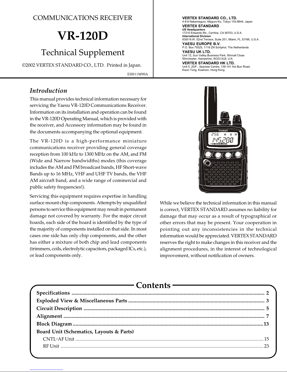
COMMUNICATIONS RECEIVER
VR-120D
Technical Supplement
©2002 VERTEX STANDARD CO., LTD. Printed in Japan.
EH011M90A
Introduction
This manual provides technical information necessary for
servicing the Yaesu VR-120D Communications Receiver.
Information on its installation and operation can be found
in the VR-120D Operating Manual, which is provided with
the receiver, and Accessory information may be found in
the documents accompanying the optional equipment.
The VR-120D is a high-performance miniature
communications receiver providing general coverage
reception from 100 kHz to 1300 MHz on the AM, and FM
(Wide and Narrow bandwidths) modes (this coverage
includes the AM and FM broadcast bands, HF Short-wave
Bands up to 16 MHz, VHF and UHF TV bands, the VHF
AM aircraft band, and a wide range of commercial and
public safety frequencies!).
VERTEX STANDARD CO., LTD.
4-8-8 Nakameguro, Meguro-Ku, Tokyo 153-8644, Japan
VERTEX STANDARD
US Headquarters
17210 Edwards Rd., Cerritos, CA 90703, U.S.A.
International Division
8350 N.W. 52nd Terrace, Suite 201, Miami, FL 33166, U.S.A.
YAESU EUROPE B.V.
P.O. Box 75525, 1118 ZN Schiphol, The Netherlands
YAESU UK LTD.
Unit 12, Sun Valley Business Park, Winnall Close
Winchester, Hampshire, SO23 0LB, U.K.
VERTEX STANDARD HK LTD.
Unit 5, 20/F., Seaview Centre, 139-141 Hoi Bun Road,
Kwun Tong, Kowloon, Hong Kong
Servicing this equipment requires expertise in handling
surface mount chip components. Attempts by unqualified
persons to service this equipment may result in permanent
damage not covered by warranty. For the major circuit
boards, each side of the board is identified by the type of
the majority of components installed on that side. In most
cases one side has only chip components, and the other
has either a mixture of both chip and lead components
(trimmers, coils, electrolytic capacitors, packaged ICs, etc.),
or lead components only.
While we believe the technical information in this manual
is correct, VERTEX STANDARD assumes no liability for
damage that may occur as a result of typographical or
other errors that may be present. Your cooperation in
pointing out any inconsistencies in the technical
information would be appreciated. VERTEX STANDARD
reserves the right to make changes in this receiver and the
alignment procedures, in the interest of technological
improvement, without notification of owners.
Contents
Specifications ............................................................................................................................................... 2
Exploded View & Miscellaneous Parts ..................................................................................................... 3
Circuit Description ...................................................................................................................................... 5
Alignment ..................................................................................................................................................... 7
Block Diagram .............................................................................................................................................13
Board Unit (Schematics, Layouts & Parts)
CNTL•AF Unit ........................................................................................................................................................ 15
RF Unit ....................................................................................................................................................................23
1
Page 2

Alignment
Note:
12
Page 3
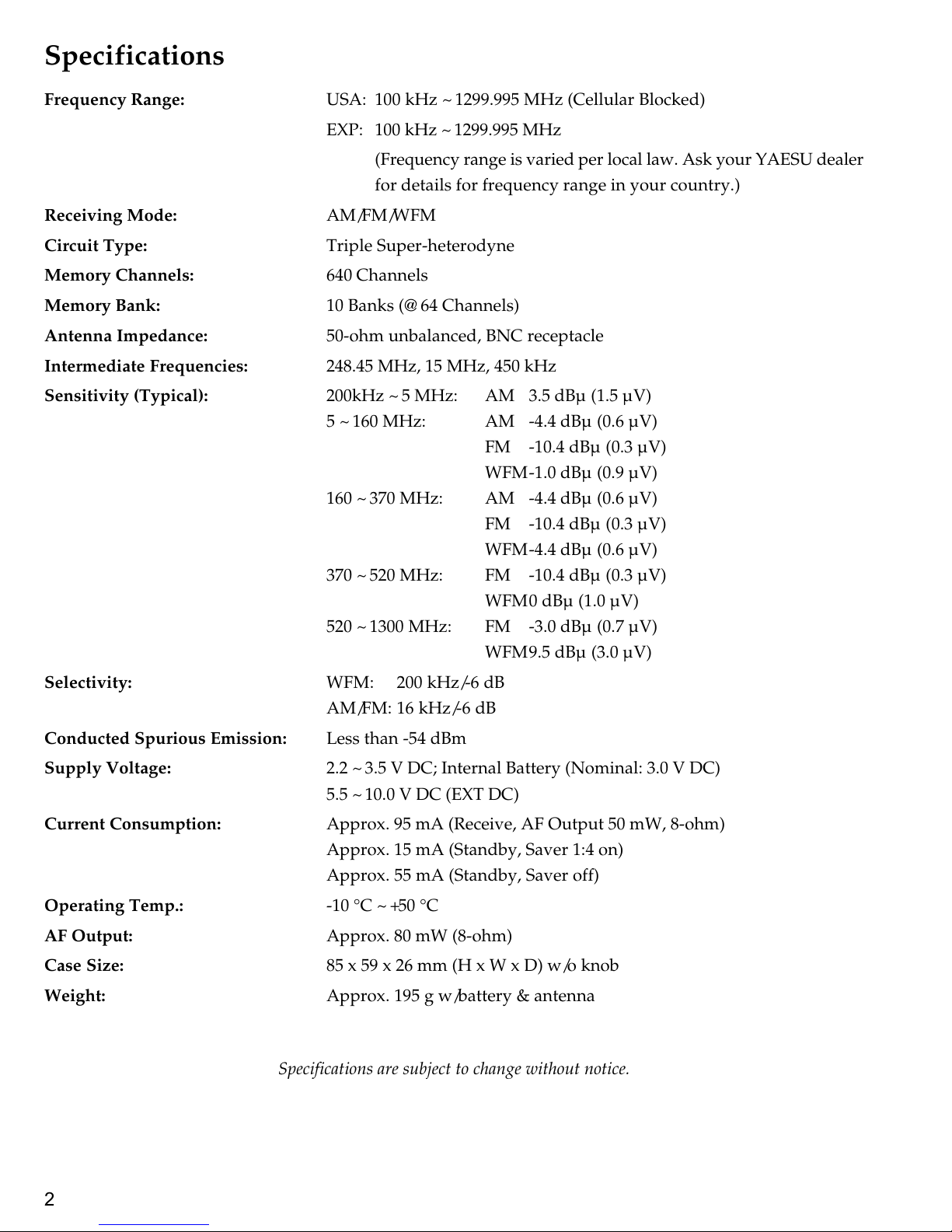
Specifications
Frequency Range: USA: 100 kHz ~ 1299.995 MHz (Cellular Blocked)
EXP: 100 kHz ~ 1299.995 MHz
(Frequency range is varied per local law. Ask your YAESU dealer
for details for frequency range in your country.)
Receiving Mode: AM/FM/WFM
Circuit Type: Triple Super-heterodyne
Memory Channels: 640 Channels
Memory Bank: 10 Banks (@ 64 Channels)
Antenna Impedance: 50-ohm unbalanced, BNC receptacle
Intermediate Frequencies: 248.45 MHz, 15 MHz, 450 kHz
Sensitivity (Typical): 200kHz ~ 5 MHz: AM 3.5 dBµ (1.5 µV)
5 ~ 160 MHz: AM -4.4 dBµ (0.6 µV)
FM -10.4 dBµ (0.3 µV)
WFM-1.0 dBµ (0.9 µV)
160 ~ 370 MHz: AM -4.4 dBµ (0.6 µV)
FM -10.4 dBµ (0.3 µV)
WFM-4.4 dBµ (0.6 µV)
370 ~ 520 MHz: FM -10.4 dBµ (0.3 µV)
WFM0 dBµ (1.0 µV)
520 ~ 1300 MHz: FM -3.0 dBµ (0.7 µV)
WFM9.5 dBµ (3.0 µV)
Selectivity: WFM: 200 kHz/-6 dB
AM/FM: 16 kHz/-6 dB
Conducted Spurious Emission: Less than -54 dBm
Supply Voltage: 2.2 ~ 3.5 V DC; Internal Battery (Nominal: 3.0 V DC)
5.5 ~ 10.0 V DC (EXT DC)
Current Consumption: Approx. 95 mA (Receive, AF Output 50 mW, 8-ohm)
Approx. 15 mA (Standby, Saver 1:4 on)
Approx. 55 mA (Standby, Saver off)
Operating Temp.: -10 °C ~ +50 °C
AF Output: Approx. 80 mW (8-ohm)
Case Size: 85 x 59 x 26 mm (H x W x D) w/o knob
Weight: Approx. 195 g w/battery & antenna
Specifications are subject to change without notice.
2
Page 4
3
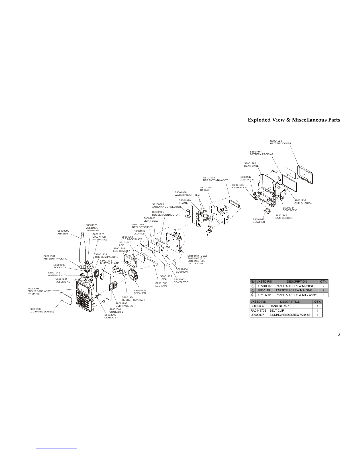
Exploded View & Miscellaneous Parts
No. VXSTD P/N DESCRIPTION QTY.
U07240307 PANHEAD SCREW M2x4B#3 2
U9900119 TAPTITE SCREW M2x5B#3 2
U07125301 PANHEAD SCREW M1.7x2.5#3 3
Â
À
Á
VXSTD P/N DESCRIPTION QTY.
S6000335 HAND STRAP 1
RA014370B BELT CLIP 1
U9900097
BINDING HEAD SCREW M3x5.5B
1
À
À
Á
Á
Â
Â
Â
S8001937
LCD PANEL (YAESU)
S8001931
ANTENNA PACKING
S8100999
ANTENNA
S8002007
FRONT CASE ASSY
(W/SP NET)
S8001941
VOLUME NUT
S8001942
NUTANTENNA
S8001930
SQL KNOB
S8001929
VOL KNOB
(W/SPRING)
S8001932
SQL GUM PACKING
S8001928
DIAL KNOB
(W/SPRING)
S8001938
BUTTON PLATE
S8001998
GUM PACKING
S8001934
RUBBER CONTACT
S8001000
SPEAKER
S8001958
LCD TAPE
S8001955
TAPE
S8002002
CONTACT C
S8002004
CUSHION
S8101164 (USA)
S8101165 (B1)
S8101166 (B2)
CNTL.AF Unit
S8100788
ANTENNA CONNECTOR
S8001939
WATER PROOF FILM
S8001999
FRAME
S8101168
RF Unit
S8101008
BAR ANTENNA ASSY
S8001736
CONTACT B
S8001947
CONTACT D
S8001996
REAR CASE
S8001944
BATTERY PACKING
S8001926
BATTERY COVER
S8001737
GUM CUSHION
S8001734
CONTACT C
S8001948
GUM CUSHION
S8001927
CLAMPER
S8002003
LIGHT SEAL
S8002005
RUBBER CONNECTOR
S8001954
REFLECT SHEET
S8001957
LCD FILE
S8001951
LCD BACK PLATE
S8101007
LCD
S8001952
LCD COVER
S8002001
CONTACT B
S8002000
CONTACT A
Page 5

Exploded View & Miscellaneous Parts
4
Note:
Page 6
Circuit Description
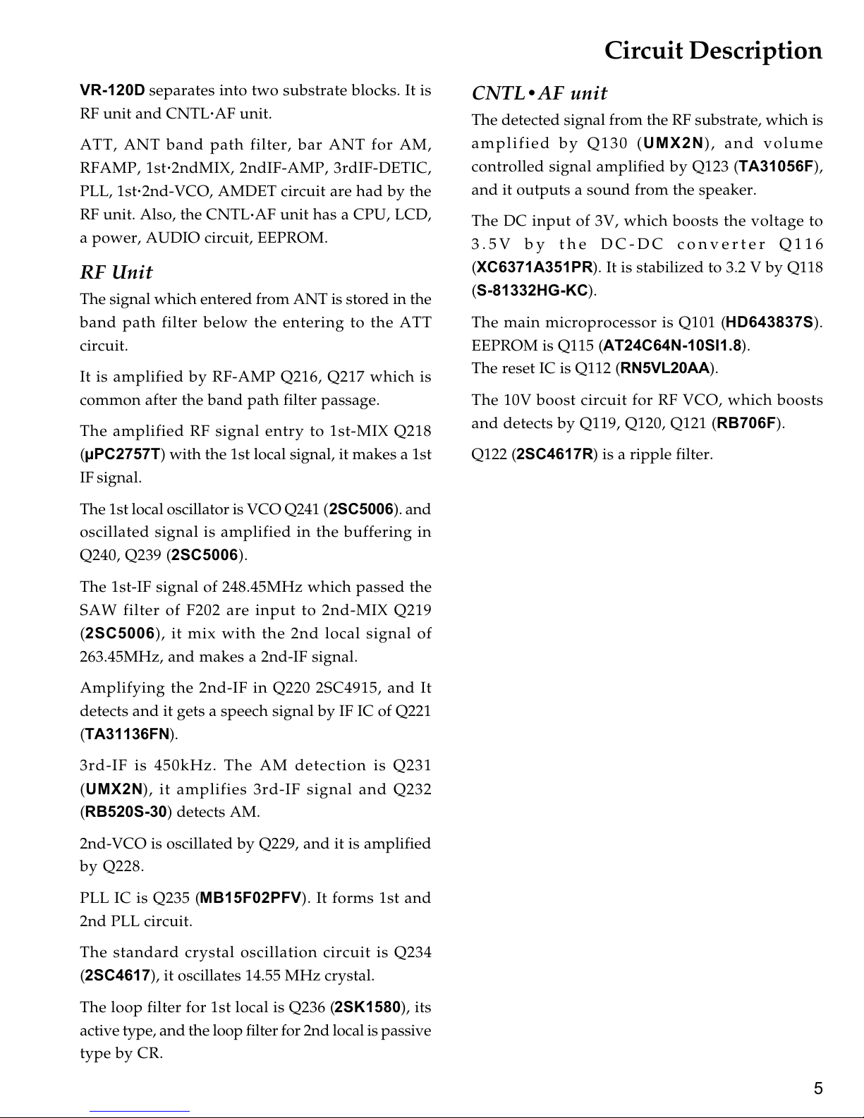
VR-120D separates into two substrate blocks. It is
RF unit and CNTL•AF unit.
ATT, ANT band path filter, bar ANT for AM,
RFAMP, 1st•2ndMIX, 2ndIF-AMP, 3rdIF-DETIC,
PLL, 1st•2nd-VCO, AMDET circuit are had by the
RF unit. Also, the CNTL•AF unit has a CPU, LCD,
a power, AUDIO circuit, EEPROM.
RF Unit
The signal which entered from ANT is stored in the
band path filter below the entering to the ATT
circuit.
It is amplified by RF-AMP Q216, Q217 which is
common after the band path filter passage.
The amplified RF signal entry to 1st-MIX Q218
(µPC2757T) with the 1st local signal, it makes a 1st
IF signal.
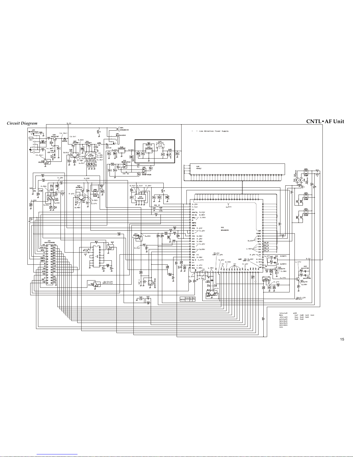
CNTL•AF unit
The detected signal from the RF substrate, which is
amplified by Q130 (UMX2N), and volume
controlled signal amplified by Q123 (TA31056F),
and it outputs a sound from the speaker.
The DC input of 3V, which boosts the voltage to
3.5V by the DC-DC converter Q116
(XC6371A351PR). It is stabilized to 3.2 V by Q118
(S-81332HG-KC).
The main microprocessor is Q101 (HD643837S).
EEPROM is Q115 (AT24C64N-10SI1.8).
The reset IC is Q112 (RN5VL20AA).
The 10V boost circuit for RF VCO, which boosts
and detects by Q119, Q120, Q121 (RB706F).
Q122 (2SC4617R) is a ripple filter.
The 1st local oscillator is VCO Q241 (2SC5006). and
oscillated signal is amplified in the buffering in
Q240, Q239 (2SC5006).
The 1st-IF signal of 248.45MHz which passed the
SAW filter of F202 are input to 2nd-MIX Q219
(2SC5006), it mix with the 2nd local signal of
263.45MHz, and makes a 2nd-IF signal.
Amplifying the 2nd-IF in Q220 2SC4915, and It
detects and it gets a speech signal by IF IC of Q221
(TA31136FN).
3rd-IF is 450kHz. The AM detection is Q231
(UMX2N), it amplifies 3rd-IF signal and Q232
(RB520S-30) detects AM.
2nd-VCO is oscillated by Q229, and it is amplified
by Q228.
PLL IC is Q235 (MB15F02PFV). It forms 1st and
2nd PLL circuit.
The standard crystal oscillation circuit is Q234
(2SC4617), it oscillates 14.55 MHz crystal.
The loop filter for 1st local is Q236 (2SK1580), its
active type, and the loop filter for 2nd local is passive
type by CR.
5
Page 7

Circuit Description
Note:
6
Page 8
Alignment
Introduction
The VR-120D has been carefully aligned at the
factory for the specified performance across the
amateur band. Realignment should therefore not
be necessary except in the event of a component
failure. All component replacement and service
should be performed only by an authorized Vertex
Standard representative, or the warranty policy may
be voided.
The following procedures cover the sometimes
critical and tedious adjustments that are not
normally required once the transceiver has left the
factory. However, if damage occurs and some parts
are replaced, realignment may be required. If a
sudden problem occurs during normal operation,
it is likely due to component failure; realignment
should not be done until after the faulty component
has been replaced.
We recommend that servicing be performed only
by authorized Vertex Standard service technicians
who are experienced with the circuitry and fully
equipped for repair and alignment. Therefore, if a
fault is suspected, contact the dealer from whom
the transceiver was purchased for instructions
regarding repair. Authorized Vertex Standard
service technicians realign all circuits and make
complete performance checks to ensure compliance
with factory specifications after replacing any faulty
components. Those who do undertake any of the
following alignments are cautioned to proceed at
their own risk. Problems caused by unauthorized
attempts at realignment are not covered by the
warranty policy. Also, Vertex Standard must reserve
the right to change circuits and alignment
procedures in the interest of improved performance,
without notifying owners. Under no circumstances
should any alignment be attempted unless the
normal function and operation of the transceiver
are clearly understood, the cause of the malfunction
has been clearly pinpointed and any faulty
components replaced, and the need for realignment
determined to be absolutely necessary.
Required Test Equipment
The following test equipment (and thorough
familiarity with its correct use) is necessary for
complete realignment. Correction of problems
caused by misalignment resulting from use of
improper test equipment is not covered under the
warranty policy. While most steps do not require
all of the equipment listed, the interactions of some
adjustments may require that more complex
adjustments be performed afterwards. Do not
attempt to perform only a single step unless it is
clearly isolated electrically from all other steps. Have
all test equipment ready before beginning, and
follow all of the steps in a section in the order
presented.
r RF Signal Generator with calibrated output level
at 1300 MHz
r Deviation Meter
r Frequency Counter: ±0.1 ppm accuracy at 500
MHz
r DC Voltmeter: high impedance
r AF Dummy Load: 8-Ohms, 1W
Note: Signal levels in dB referred to in this procedure
are based on 0 dBµ = 0.5 µV (closed circuit).
Alignment Preparation & Precautions
Correct alignment requires that the ambient
temperature in the repair shop be the same as that
of the receiver and test equipment, and that this
temperature be held constant between 20 °C and
30 °C (68° ~ 86° F). When the receiver is brought
into the shop from hot or cold air it should be
allowed some time for thermal equalization with
the environment before alignment. If possible,
alignments should be made with oscillator shields
and circuit boards firmly affixed in place. Also, the
test equipment must be thoroughly warmed up
before beginning.
7
Page 9
Alignment
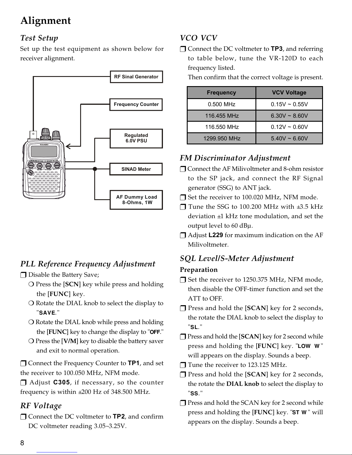
AF Dummy Load
Frequency Counter
RF Sinal Generator
SINAD Meter
Regulated
Test Setup
Set up the test equipment as shown below for
receiver alignment.
6.0V PSU
8-Ohms, 1W
VCO VCV
r Connect the DC voltmeter to TP3, and referring
to table below, tune the VR-120D to each
frequency listed.
Then confirm that the correct voltage is present.
Frequency VCV Voltage
0.500 MHz 0.15V ~ 0.55V
116.455 MHz 6.30V ~ 8.60V
116.550 MHz 0.12V ~ 0.60V
1299.950 MHz 5.40V ~ 6.60V
FM Discriminator Adjustment
r Connect the AF Milivoltmeter and 8-ohm resistor
to the SP jack, and connect the RF Signal
generator (SSG) to ANT jack.
r Set the receiver to 100.020 MHz, NFM mode.
r Tune the SSG to 100.200 MHz with ±3.5 kHz
deviation ±1 kHz tone modulation, and set the
output level to 60 dBµ.
r Adjust L229 for maximum indication on the AF
Milivoltmeter.
PLL Reference Frequency Adjustment
r Disable the Battery Save;
m Press the [SCN] key while press and holding
the [FUNC] key.
m Rotate the DIAL knob to select the display to
"SAVE."
m Rotate the DIAL knob while press and holding
the [FUNC] key to change the display to "OFF."
m Press the [V/M] key to disable the battery saver
and exit to normal operation.
r Connect the Frequency Counter to TP1, and set
the receiver to 100.050 MHz, NFM mode.
r Adjust C305, if necessary, so the counter
frequency is within ±200 Hz of 348.500 MHz.
RF Voltage
r Connect the DC voltmeter to TP2, and confirm
DC voltmeter reading 3.05~3.25V.
SQL Level/S-Meter Adjustment
Preparation
r Set the receiver to 1250.375 MHz, NFM mode,
then disable the OFF-timer function and set the
ATT to OFF.
r Press and hold the [SCAN] key for 2 seconds,
the rotate the DIAL knob to select the display to
"SL."
r Press and hold the [SCAN] key for 2 second while
press and holding the [FUNC] key. "LOW W "
will appears on the display. Sounds a beep.
r Tune the receiver to 123.125 MHz.
r Press and hold the [SCAN] key for 2 seconds,
the rotate the DIAL knob to select the display to
"SS."
r Press and hold the SCAN key for 2 second while
press and holding the [FUNC] key. "ST W " will
appears on the display. Sounds a beep.
8
Page 10

Alignment Points
L229
FM Discriminator Adjust
Alignment
TP3
VCO VCV:
DC voltmeter
TP2
RF Voltege:
DC voltmeter
C305
PLL Reference Frequency Adjust
TP1
PLL Reference Frequency Adjust:
Frequency Counter
9
Page 11

Alignment
r Tune the receiver to 448.250 MHz.
r Press and hold the [SCAN] key for 2 seconds,
the rotate the DIAL knob to select the display to
"SU."
r Press and hold the [SCAN] key for 2 second while
press and holding the [FUNC] key. "SQL SET"
will appears on the display. Sounds a beep.
SQL Level Adjustment
NFM mode:
r Connect the RF Signal Generator to ANT jack.
r Set the receiver to 100.050 MHz, NFM mode.
r Press the [SCAN] key. "SQL" will appear on the
display.
r Tune the SSG to 100.050 MHz with ±3.5 kHz
deviation @1 kHz tone modulation, and set the
output level to -12 dBµ.
r Press the [BND(p)] key while press and holding
[FUNC] key. "SQL SL" will appear on the display.
r Press the [V/M] key while press and holding
[FUNC] key. Sounds a beep.
r Increase the SSG output level to 2 dBµ.
r Press the [SCAN] key while press and holding
[FUNC] key. "SQL TI" will appear on the display.
r Press the [V/M] key while press and holding
[FUNC] key. Sounds a beep.
r Press the [MODE] key while press and holding
[FUNC] key. "SQL CR" will appear on the
display.
r Press the [V/M] key while press and holding
[FUNC] key. Sounds a beep.
WFM mode:
r Set the receiver to 100.050 MHz, WFM mode.
r Press the [SCAN] key. "SQL" will appear on the
display.
r Tune the SSG to 100.050 MHz with ±75 kHz
deviation @1 kHz tone modulation, and set the
output level to 2 dBµ.
r Press the [BND(p)] key while press and holding
[FUNC] key. "SQL SL" will appear on the display.
r Press the [V/M] key while press and holding
[FUNC] key. Sounds a beep.
r Increase the SSG output level to 15 dBµ.
r Press the [SCAN] key while press and holding
[FUNC] key. "SQL TI" will appear on the display.
r Press the [V/M] key while press and holding
[FUNC] key. Sounds a beep.
r Press the [MODE] key while press and holding
[FUNC] key. "SQL CR" will appear on the
display.
r Press the [V/M] key while press and holding
[FUNC] key. Sounds a beep.
AM mode:
r Set the receiver to 1.050 MHz, AM mode.
r Press the [SCAN] key. "SQL" will appear on the
display.
r Tune the SSG to 1.050 MHz with 30%
modulation @1 kHz tone, and set the output level
to -5 dBµ.
r Press the [BND(p)] key while press and holding
[FUNC] key. "SQL SL" will appear on the display.
r Press the [V/M] key while press and holding
[FUNC] key. Sounds a beep.
r Increase the SSG output level to 8 dBµ.
r Press the [SCAN] key while press and holding
[FUNC] key. "SQL TI" will appear on the display.
r Press the [V/M] key while press and holding
[FUNC] key. Sounds a beep.
r Press the [MODE] key while press and holding
[FUNC] key. "SQL CR" will appear on the
display.
r Press the [V/M] key while press and holding
[FUNC] key. Sounds a beep.
S-Meter Adjustment
NFM mode:
r Connect the RF Signal Generator to ANT jack.
r Set the receiver to 100.050 MHz, NFM mode.
r Press the [BND(p)]. "S M ET" will appear on the
display.
r Tune the SSG to 100.050 MHz with ±3.5 kHz
deviation @1 kHz tone modulation, and set the
output level to 20 dBµ.
10
Page 12
Alignment
r Press the [BND(p)] key while press and holding
[FUNC] key. "S M ET+ " will appear on the
display.
r Press the [V/M] key while press and holding
[FUNC] key. Sounds a beep.
r Reduce the SSG output level to -5 dBµ.
r Press the [SCAN] key while press and holding
[FUNC] key. "S M ET2 " will appear on the
display.
r Press the [V/M] key while press and holding
[FUNC] key. Sounds a beep.
WFM mode:
r Set the receiver to 100.050 MHz, WFM mode.
r Press the [BND(p)]. "S M ET" will appear on the
display.
r Tune the SSG to 100.050 MHz with ±75 kHz
deviation @1 kHz tone modulation, and set the
output level to 35 dBµ.
r Press the [BND(p)] key while press and holding
[FUNC] key. "S M ET+ " will appear on the
display.
r Press the [V/M] key while press and holding
[FUNC] key. Sounds a beep.
r Reduce the SSG output level to 5 dBµ.
r Press the [SCAN] key while press and holding
[FUNC] key. "S M ET2 " will appear on the
display.
r Press the [V/M] key while press and holding
[FUNC] key. Sounds a beep.
AM mode:
r Set the receiver to 1.050 MHz, AM mode.
r Press the [BND(p)]. "S M ET" will appear on the
display.
r Tune the SSG to 1.050 MHz with 30%
modulation @1 kHz tone, and set the output level
to 20 dBµ.
r Press the [BND(p)] key while press and holding
[FUNC] key. "S M ET+ " will appear on the
display.
r Press the [V/M] key while press and holding
[FUNC] key. Sounds a beep.
r Reduce the SSG output level to 0 dBµ.
r Press the [SCAN] key while press and holding
[FUNC] key. "S M ET2 " will appear on the
display.
r Press the [V/M] key while press and holding
[FUNC] key. Sounds a beep.
Press the [V/M] key to save the new setting and
exit to the normal operation.
11
Page 13
13
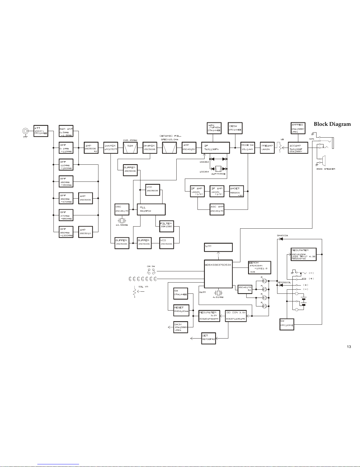
Block Diagram
Page 14

14
Block Diagram
Note:
Page 15
15
CNTL•AF Unit
Circuit Diagram
USA B1 B2
R113 --- 0 ---
Page 16

16
CNTL•AF Unit
Note:
Page 17
17
CNTL•AF Unit
Side A
A B C D E
1
2
3
4
Parts Layout
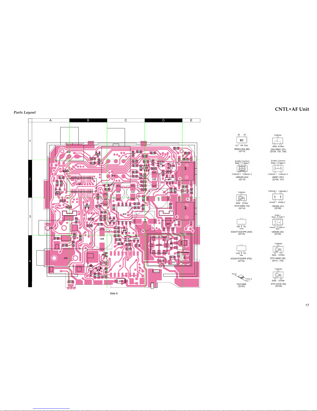
RN5VL20A (B0)
(Q112)
UMG2N (G2)
(Q113)
DTA144EE (16)
(Q114)
DTC144EE (26)
(Q131, 142)
XC6371A351PR (A35)
(Q116)
TA31056F
(Q123)
2SA1588Y (ZY)
(Q124, 125, 128)
UMW1 (W1)
(Q126, 127)
UMX2N (X2)
(Q130)
1SS382 (A1)
(Q129)
XC6201P322PR (P32)
(Q118)
DTC123YE (62)
(Q139)
Page 18
18
CNTL•AF Unit
Side B
e d c b a
1
2
3
4
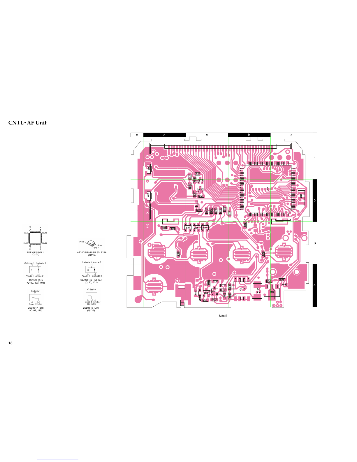
HD6433837SD
(Q101)
1SS382 (A1)
(Q102, 103, 104)
2SC4617 (BR)
(Q107, 110)
RB706F-40T106 (3J)
(Q120, 121)
AT24C64N-10SI1.8SL722A
(Q115)
2SD1615 (GK)
(Q136)
Page 19
Parts List
DESCRIPTION VALUE V/W TOL. VXSTD P/NMFR’S DESIG VERS.REF. LOT. LAY ADR
PCB with Component (W/ LCD ASS'Y, SHIELD CASE, CUSHION, CONTACT C) S8101164 USA
PCB with Component (W/ LCD ASS'Y, SHIELD CASE, CUSHION, CONTACT C) S8101165 B1
PCB with Component (W/ LCD ASS'Y, SHIELD CASE, CUSHION, CONTACT C) S8101166 B2
C101 CHIP CAP. 47pF 50V CH GRM39CH470J50PT K22174227 1-
C102 CHIP CAP. 47pF 50V CH GRM39CH470J50PT K22174227 1-
C103 CHIP CAP. 0.22uF 16V B GRM40B224M16PT K22120806 1-
C104 CHIP CAP. 0.33uF 10V B GRM188B11A334KA01D K22104802 1-
C105 CHIP CAP. 0.1uF 16V B GRM39B104K16PT K22124805 1-
C108 CHIP CAP. 0.001uF 50V B GRM39B102K50PT K22174821 1-
C109 CHIP CAP. 0.001uF 50V B GRM39B102K50PT K22174821 1-
C110 CHIP CAP. 0.1uF 16V B GRM39B104K16PT K22124805 1-
C111 CHIP CAP. 0.001uF 50V B GRM39B102K50PT K22174821 1-
C112 CHIP CAP. 0.01uF 25V B GRM39B103K25PT K22144803 1-
C113 CHIP TA.CAP. 10uF 6.3V TEMSVA0J106M-8R K78080027 1-
C114 CHIP CAP. 0.01uF 25V B GRM39B103K25PT K22144803 1-
C115 CHIP CAP. 0.01uF 25V B GRM39B103K25PT K22144803 1-
C116 CHIP TA.CAP. 33uF 10V TEMSVB21A336M-8R K78100047 1-
C118 CHIP CAP. 0.1uF 16V B GRM39B104K16PT K22124805 1-
C119 CHIP CAP. 0.1uF 16V B GRM39B104K16PT K22124805 1-
C120 CHIP CAP. 0.1uF 16V B GRM39B104K16PT K22124805 1-
C121 CHIP CAP. 0.1uF 16V B GRM39B104K16PT K22124805 1-
C122 CHIP CAP. 0.1uF 16V B GRM39B104K16PT K22124805 1-
C123 CHIP TA.CAP. 220uF 4V UZS0G221MCR1GB K48060006 1-
C124 CHIP CAP. 0.01uF 25V B GRM39B103K25PT K22144803 1-
C125 CHIP CAP. 0.1uF 16V B GRM39B104K16PT K22124805 1-
C127 CHIP CAP. 0.1uF 16V B GRM39B104K16PT K22124805 1-
C128 CHIP CAP. 0.1uF 16V B GRM39B104K16PT K22124805 1-
C129 CHIP TA.CAP. 220uF 4V UZS0G221MCR1GB K48060006 1-
C130 CHIP TA.CAP. 100uF 6.3V UZS0J101MCR1GB K48080009 1-
C131 CHIP CAP. 100pF 50V CH GRM39CH101J50PT K22174235 1-
C132 CHIP TA.CAP. 2.2uF 50V UWX1H2R2MCR1GB K48170010 1-
C133 CHIP TA.CAP. 4.7uF 25V UWX1E4R7MCR1GB K48140012 1-
C134 CHIP CAP. 0.027uF 16V R GRM39R273K16PT K22124802 1-
C135 CHIP CAP. 0.047uF 16V B GRM39B473K16PT K22124804 1-
C136 CHIP CAP. 0.1uF 16V B GRM39B104K16PT K22124805 1-
C137 CHIP CAP. 1uF 6.3V B GRM39B105K6.3PT K22084801 1-
C138 CHIP TA.CAP. 4.7uF 25V UWX1E4R7MCR1GB K48140012 1-
C139 CHIP CAP. 0.1uF 16V B GRM39B104K16PT K22124805 1-
C140 CHIP CAP. 0.027uF 16V R GRM39R273K16PT K22124802 1-
C141 CHIP CAP. 1uF 6.3V B GRM39B105K6.3PT K22084801 1-
C142 AL.ELECTRO.CAP. 10uF 16V UWX1C100MCR2GB K48120016 1-
C145 CHIP CAP. 0.1uF 16V B GRM39B104K16PT K22124805 1-
E101 SPEAKER K036NA500-35 S8101000 1-
J101 CONNECTOR 245047030400856 P1091121 1-
J102 CONNECTOR HSJ1501-010010 P1091068 1-
J103 CONNECTOR HEC3350-012110 P0091167 1-
L101 M.RFC MLF1608A1R0KT L1690930 1-
L102 M.RFC LB2016T4R7M L1691089 1-
L103 RF TRANS. S-167-3779 S8100775 1-
L104 M.RFC MLF1608A1R0KT L1690930 1-
L105 M.RFC MLF1608A1R0KT L1690930 1-
Q101 IC HD6433837SD53X S8101016 USA 1- b2
Q101 IC HD6433837SD48X S8101013 B1 1- b2
Q101 IC HD6433837SD48X S8101013 B2 1- b2
Q102 DIODE 1SS382(TE85R) G2070732 1- c3
Q103 DIODE 1SS382(TE85R) G2070732 1- c3
Q104 DIODE 1SS382(TE85R) G2070732 1- c3
Q105 LED AA1111C-640-TR S8101158 1- b3
Q106 LED AA1111C-640-TR S8101158 1- d3
Q107 TRANSISTOR 2SC4617 TL R G3346178R 1- c2
Q108 LED CL-220Y-C G2070830 1- d1
Q109 LED CL-220Y-C G2070830 1- d2
Q110 TRANSISTOR 2SC4617 TL R G3346178R 1- c2
Q112 IC RN5VL20AA-TR G1093071 1- D2
Q113 TRANSISTOR UMG2N TR G3070088 1- A2
Q114 TRANSISTOR DTA144EE TL G3070074 1- B1
Q115 IC AT24C64N-10SI1.8SL722A G1093171 1- b4
CNTL•AF Unit
19
Page 20
CNTL•AF Unit
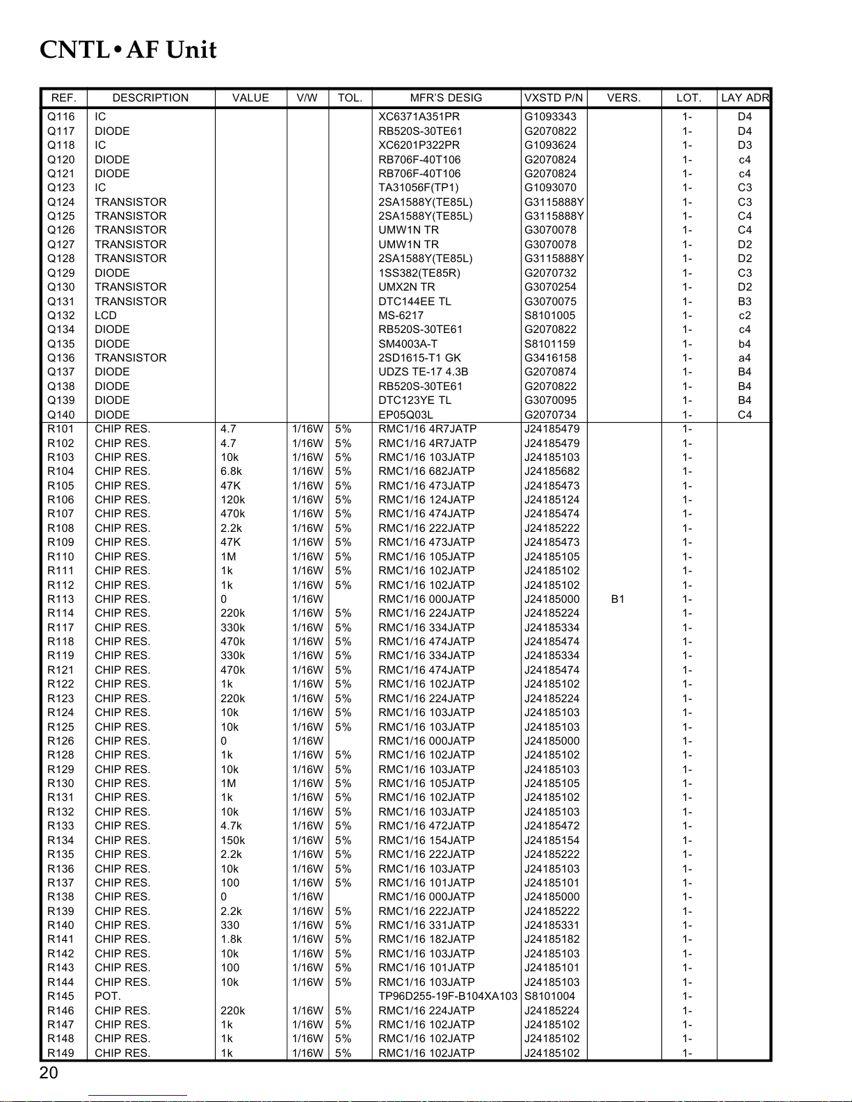
DESCRIPTION VALUE V/W TOL. VXSTD P/NMFR’S DESIG VERS.REF. LOT. LAY ADR
Q116 IC XC6371A351PR G1093343 1- D4
Q117 DIODE RB520S-30TE61 G2070822 1- D4
Q118 IC XC6201P322PR G1093624 1- D3
Q120 DIODE RB706F-40T106 G2070824 1- c4
Q121 DIODE RB706F-40T106 G2070824 1- c4
Q123 IC TA31056F(TP1) G1093070 1- C3
Q124 TRANSISTOR 2SA1588Y(TE85L) G3115888Y 1- C3
Q125 TRANSISTOR 2SA1588Y(TE85L) G3115888Y 1- C4
Q126 TRANSISTOR UMW1N TR G3070078 1- C4
Q127 TRANSISTOR UMW1N TR G3070078 1- D2
Q128 TRANSISTOR 2SA1588Y(TE85L) G3115888Y 1- D2
Q129 DIODE 1SS382(TE85R) G2070732 1- C3
Q130 TRANSISTOR UMX2N TR G3070254 1- D2
Q131 TRANSISTOR DTC144EE TL G3070075 1- B3
Q132 LCD MS-6217 S8101005 1- c2
Q134 DIODE RB520S-30TE61 G2070822 1- c4
Q135 DIODE SM4003A-T S8101159 1- b4
Q136 TRANSISTOR 2SD1615-T1 GK G3416158 1- a4
Q137 DIODE UDZS TE-17 4.3B G2070874 1- B4
Q138 DIODE RB520S-30TE61 G2070822 1- B4
Q139 DIODE DTC123YE TL G3070095 1- B4
Q140 DIODE EP05Q03L G2070734 1- C4
R101 CHIP RES. 4.7 1/16W 5% RMC1/16 4R7JATP J24185479 1-
R102 CHIP RES. 4.7 1/16W 5% RMC1/16 4R7JATP J24185479 1-
R103 CHIP RES. 10k 1/16W 5% RMC1/16 103JATP J24185103 1-
R104 CHIP RES. 6.8k 1/16W 5% RMC1/16 682JATP J24185682 1-
R105 CHIP RES. 47K 1/16W 5% RMC1/16 473JATP J24185473 1-
R106 CHIP RES. 120k 1/16W 5% RMC1/16 124JATP J24185124 1-
R107 CHIP RES. 470k 1/16W 5% RMC1/16 474JATP J24185474 1-
R108 CHIP RES. 2.2k 1/16W 5% RMC1/16 222JATP J24185222 1-
R109 CHIP RES. 47K 1/16W 5% RMC1/16 473JATP J24185473 1-
R110 CHIP RES. 1M 1/16W 5% RMC1/16 105JATP J24185105 1-
R111 CHIP RES. 1k 1/16W 5% RMC1/16 102JATP J24185102 1-
R112 CHIP RES. 1k 1/16W 5% RMC1/16 102JATP J24185102 1-
R113 CHIP RES. 0 1/16W RMC1/16 000JATP J24185000 B1 1-
R114 CHIP RES. 220k 1/16W 5% RMC1/16 224JATP J24185224 1-
R117 CHIP RES. 330k 1/16W 5% RMC1/16 334JATP J24185334 1-
R118 CHIP RES. 470k 1/16W 5% RMC1/16 474JATP J24185474 1-
R119 CHIP RES. 330k 1/16W 5% RMC1/16 334JATP J24185334 1-
R121 CHIP RES. 470k 1/16W 5% RMC1/16 474JATP J24185474 1-
R122 CHIP RES. 1k 1/16W 5% RMC1/16 102JATP J24185102 1-
R123 CHIP RES. 220k 1/16W 5% RMC1/16 224JATP J24185224 1-
R124 CHIP RES. 10k 1/16W 5% RMC1/16 103JATP J24185103 1-
R125 CHIP RES. 10k 1/16W 5% RMC1/16 103JATP J24185103 1-
R126 CHIP RES. 0 1/16W RMC1/16 000JATP J24185000 1-
R128 CHIP RES. 1k 1/16W 5% RMC1/16 102JATP J24185102 1-
R129 CHIP RES. 10k 1/16W 5% RMC1/16 103JATP J24185103 1-
R130 CHIP RES. 1M 1/16W 5% RMC1/16 105JATP J24185105 1-
R131 CHIP RES. 1k 1/16W 5% RMC1/16 102JATP J24185102 1-
R132 CHIP RES. 10k 1/16W 5% RMC1/16 103JATP J24185103 1-
R133 CHIP RES. 4.7k 1/16W 5% RMC1/16 472JATP J24185472 1-
R134 CHIP RES. 150k 1/16W 5% RMC1/16 154JATP J24185154 1-
R135 CHIP RES. 2.2k 1/16W 5% RMC1/16 222JATP J24185222 1-
R136 CHIP RES. 10k 1/16W 5% RMC1/16 103JATP J24185103 1-
R137 CHIP RES. 100 1/16W 5% RMC1/16 101JATP J24185101 1-
R138 CHIP RES. 0 1/16W RMC1/16 000JATP J24185000 1-
R139 CHIP RES. 2.2k 1/16W 5% RMC1/16 222JATP J24185222 1-
R140 CHIP RES. 330 1/16W 5% RMC1/16 331JATP J24185331 1-
R141 CHIP RES. 1.8k 1/16W 5% RMC1/16 182JATP J24185182 1-
R142 CHIP RES. 10k 1/16W 5% RMC1/16 103JATP J24185103 1-
R143 CHIP RES. 100 1/16W 5% RMC1/16 101JATP J24185101 1-
R144 CHIP RES. 10k 1/16W 5% RMC1/16 103JATP J24185103 1-
R145 POT. TP96D255-19F-B104XA103 S8101004 1-
R146 CHIP RES. 220k 1/16W 5% RMC1/16 224JATP J24185224 1-
R147 CHIP RES. 1k 1/16W 5% RMC1/16 102JATP J24185102 1-
R148 CHIP RES. 1k 1/16W 5% RMC1/16 102JATP J24185102 1-
R149 CHIP RES. 1k 1/16W 5% RMC1/16 102JATP J24185102 1-
20
Page 21
CNTL•AF Unit
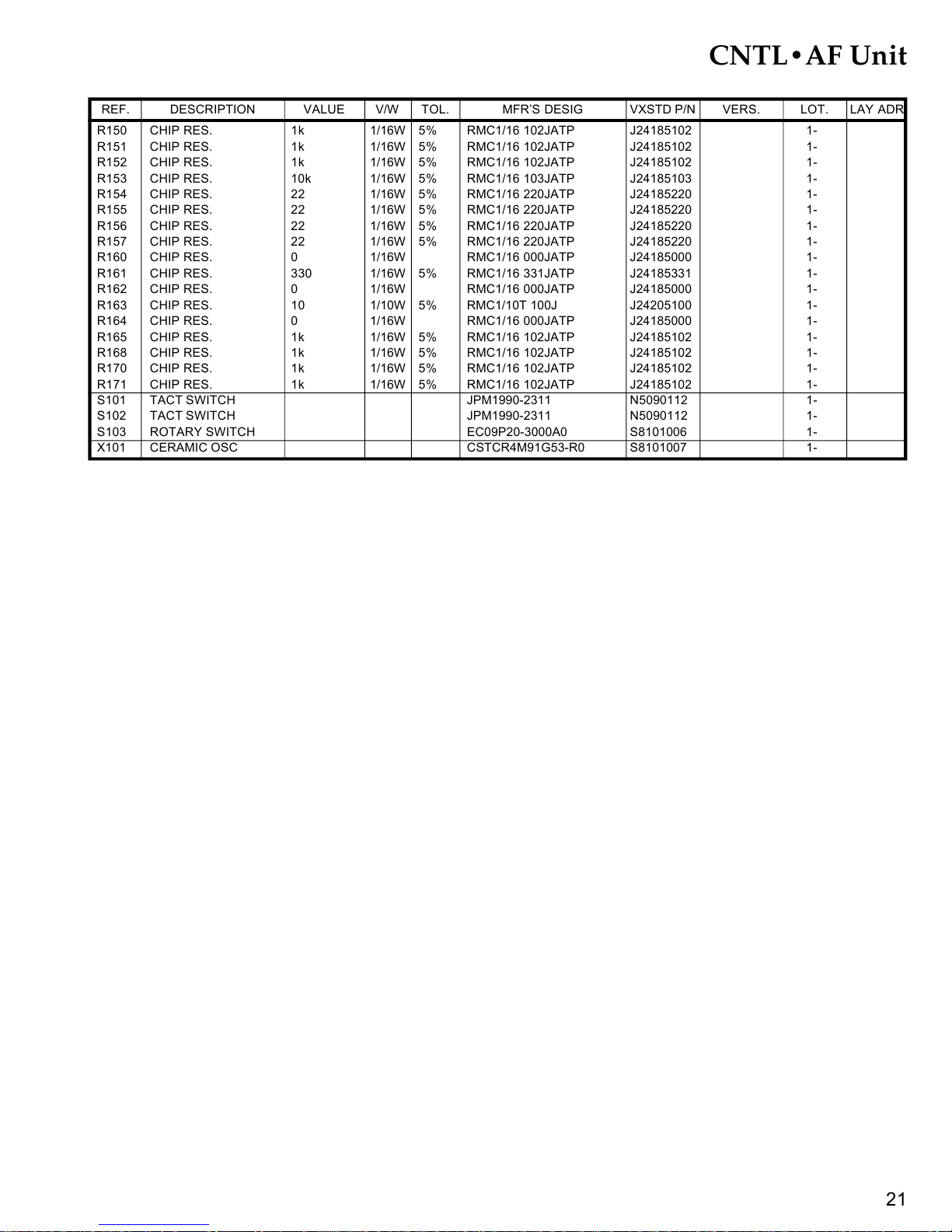
DESCRIPTION VALUE V/W TOL. VXSTD P/NMFR’S DESIG VERS.REF. LOT. LAY ADR
R150 CHIP RES. 1k 1/16W 5% RMC1/16 102JATP J24185102 1-
R151 CHIP RES. 1k 1/16W 5% RMC1/16 102JATP J24185102 1-
R152 CHIP RES. 1k 1/16W 5% RMC1/16 102JATP J24185102 1-
R153 CHIP RES. 10k 1/16W 5% RMC1/16 103JATP J24185103 1-
R154 CHIP RES. 22 1/16W 5% RMC1/16 220JATP J24185220 1-
R155 CHIP RES. 22 1/16W 5% RMC1/16 220JATP J24185220 1-
R156 CHIP RES. 22 1/16W 5% RMC1/16 220JATP J24185220 1-
R157 CHIP RES. 22 1/16W 5% RMC1/16 220JATP J24185220 1-
R160 CHIP RES. 0 1/16W RMC1/16 000JATP J24185000 1-
R161 CHIP RES. 330 1/16W 5% RMC1/16 331JATP J24185331 1-
R162 CHIP RES. 0 1/16W RMC1/16 000JATP J24185000 1-
R163 CHIP RES. 10 1/10W 5% RMC1/10T 100J J24205100 1-
R164 CHIP RES. 0 1/16W RMC1/16 000JATP J24185000 1-
R165 CHIP RES. 1k 1/16W 5% RMC1/16 102JATP J24185102 1-
R168 CHIP RES. 1k 1/16W 5% RMC1/16 102JATP J24185102 1-
R170 CHIP RES. 1k 1/16W 5% RMC1/16 102JATP J24185102 1-
R171 CHIP RES. 1k 1/16W 5% RMC1/16 102JATP J24185102 1-
S101 TACT SWITCH JPM1990-2311 N5090112 1-
S102 TACT SWITCH JPM1990-2311 N5090112 1-
S103 ROTARY SWITCH EC09P20-3000A0 S8101006 1-
X101 CERAMIC OSC CSTCR4M91G53-R0 S8101007 1-
21
Page 22
CNTL•AF Unit
Note:
22
Page 23
23
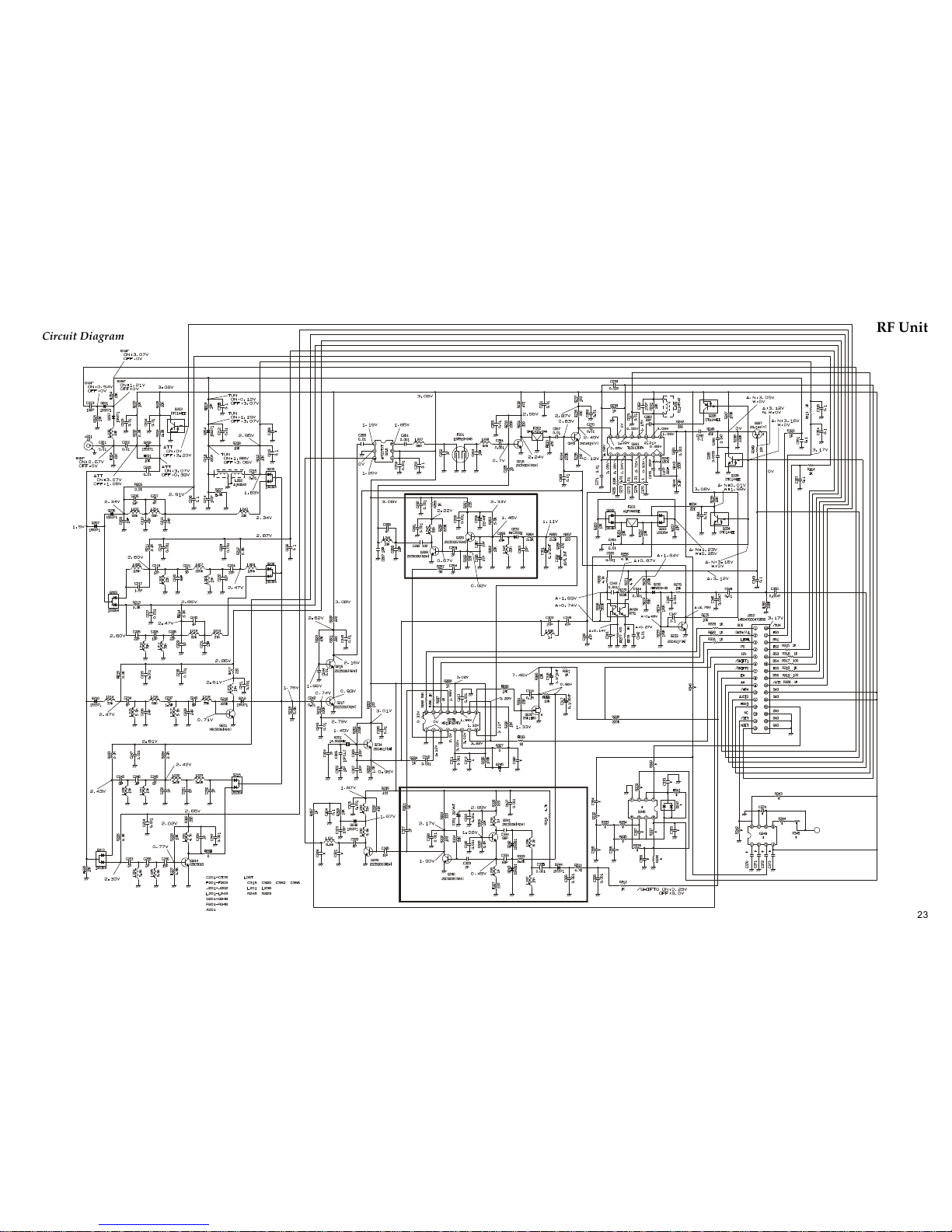
RF Unit
Circuit Diagram
Page 24

24
RF Unit
Note:
Page 25
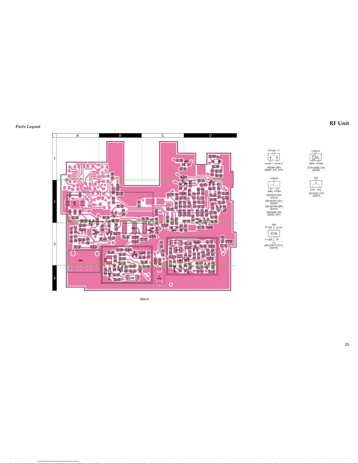
25
RF Unit
Side A
A B C D
1
2
3
4
Parts Layout
1SS364 (BF)
(Q205, 213, 215)
µPC2757T (C1Y)
(Q218)
DTA144EE (16)
(Q225)
2SJ144Y (VY)
(Q227)
2SC5010 (83)
(Q214)
2SC4915Y (QY)
(Q220)
2SC4617R (BR)
(Q233)
2SC5006 (24)
(Q240, 241)
Page 26
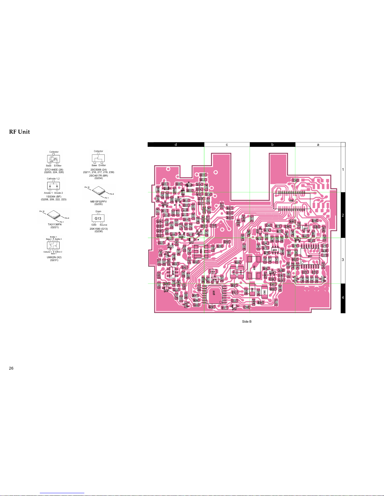
26
RF Unit
Side B
1
2
3
4
d c b a
1SS364 (BF)
(Q208, 209, 222, 223)
DTC144EE (26)
(Q203, 224, 226)
2SC5006 (24)
(Q211, 216, 217, 219, 239)
2SC4617R (BR)
(Q234)
TA31136FN
(Q221)
UMX2N (X2)
(Q231)
MB15F02PFV
(Q235)
2SK1580 (G13)
(Q236)
Page 27
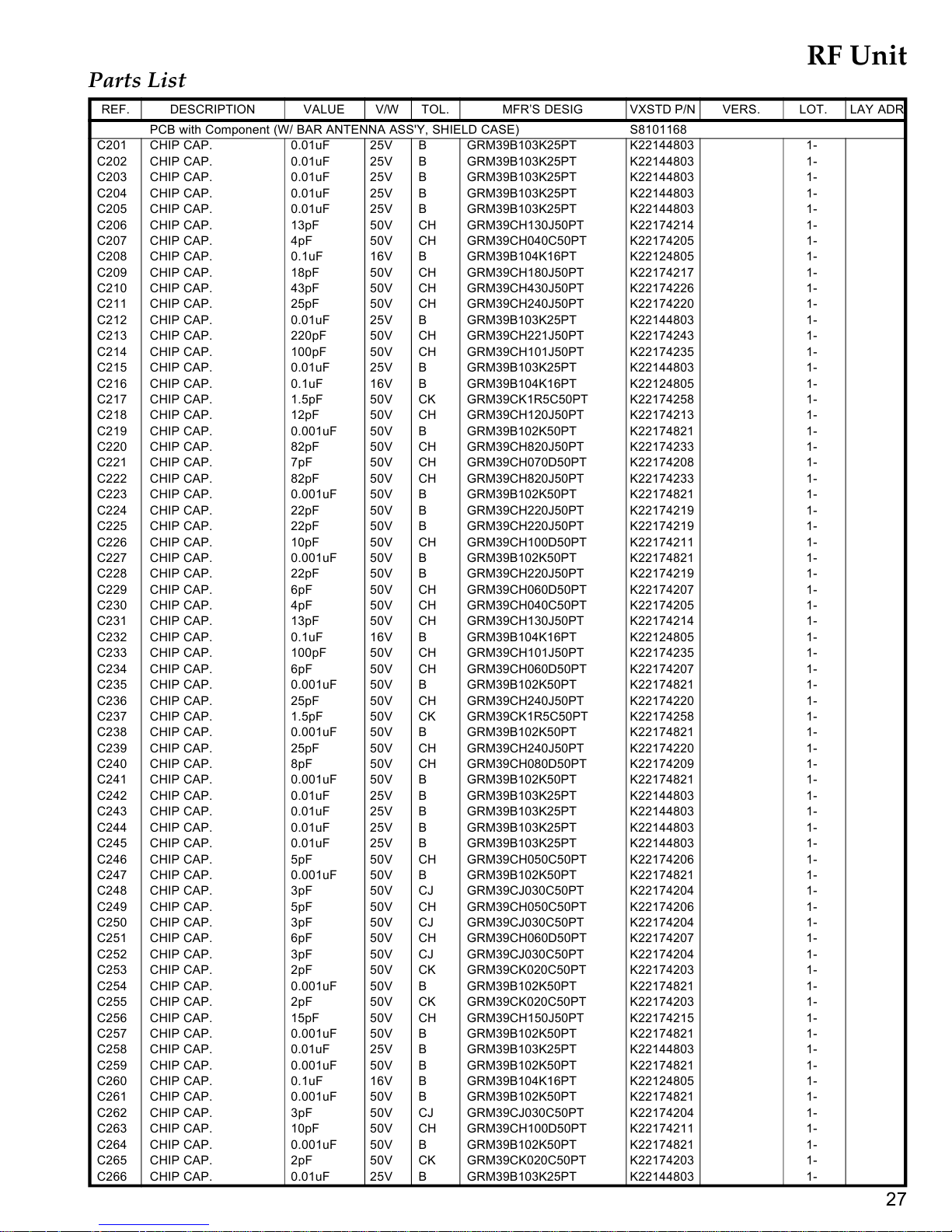
Parts List
DESCRIPTION VALUE V/W TOL. VXSTD P/NMFR’S DESIG VERS.REF. LOT. LAY ADR
PCB with Component (W/ BAR ANTENNA ASS'Y, SHIELD CASE) S8101168
C201 CHIP CAP. 0.01uF 25V B GRM39B103K25PT K22144803 1-
C202 CHIP CAP. 0.01uF 25V B GRM39B103K25PT K22144803 1-
C203 CHIP CAP. 0.01uF 25V B GRM39B103K25PT K22144803 1-
C204 CHIP CAP. 0.01uF 25V B GRM39B103K25PT K22144803 1-
C205 CHIP CAP. 0.01uF 25V B GRM39B103K25PT K22144803 1-
C206 CHIP CAP. 13pF 50V CH GRM39CH130J50PT K22174214 1-
C207 CHIP CAP. 4pF 50V CH GRM39CH040C50PT K22174205 1-
C208 CHIP CAP. 0.1uF 16V B GRM39B104K16PT K22124805 1-
C209 CHIP CAP. 18pF 50V CH GRM39CH180J50PT K22174217 1-
C210 CHIP CAP. 43pF 50V CH GRM39CH430J50PT K22174226 1-
C211 CHIP CAP. 25pF 50V CH GRM39CH240J50PT K22174220 1-
C212 CHIP CAP. 0.01uF 25V B GRM39B103K25PT K22144803 1-
C213 CHIP CAP. 220pF 50V CH GRM39CH221J50PT K22174243 1-
C214 CHIP CAP. 100pF 50V CH GRM39CH101J50PT K22174235 1-
C215 CHIP CAP. 0.01uF 25V B GRM39B103K25PT K22144803 1-
C216 CHIP CAP. 0.1uF 16V B GRM39B104K16PT K22124805 1-
C217 CHIP CAP. 1.5pF 50V CK GRM39CK1R5C50PT K22174258 1-
C218 CHIP CAP. 12pF 50V CH GRM39CH120J50PT K22174213 1-
C219 CHIP CAP. 0.001uF 50V B GRM39B102K50PT K22174821 1-
C220 CHIP CAP. 82pF 50V CH GRM39CH820J50PT K22174233 1-
C221 CHIP CAP. 7pF 50V CH GRM39CH070D50PT K22174208 1-
C222 CHIP CAP. 82pF 50V CH GRM39CH820J50PT K22174233 1-
C223 CHIP CAP. 0.001uF 50V B GRM39B102K50PT K22174821 1-
C224 CHIP CAP. 22pF 50V B GRM39CH220J50PT K22174219 1-
C225 CHIP CAP. 22pF 50V B GRM39CH220J50PT K22174219 1-
C226 CHIP CAP. 10pF 50V CH GRM39CH100D50PT K22174211 1-
C227 CHIP CAP. 0.001uF 50V B GRM39B102K50PT K22174821 1-
C228 CHIP CAP. 22pF 50V B GRM39CH220J50PT K22174219 1-
C229 CHIP CAP. 6pF 50V CH GRM39CH060D50PT K22174207 1-
C230 CHIP CAP. 4pF 50V CH GRM39CH040C50PT K22174205 1-
C231 CHIP CAP. 13pF 50V CH GRM39CH130J50PT K22174214 1-
C232 CHIP CAP. 0.1uF 16V B GRM39B104K16PT K22124805 1-
C233 CHIP CAP. 100pF 50V CH GRM39CH101J50PT K22174235 1-
C234 CHIP CAP. 6pF 50V CH GRM39CH060D50PT K22174207 1-
C235 CHIP CAP. 0.001uF 50V B GRM39B102K50PT K22174821 1-
C236 CHIP CAP. 25pF 50V CH GRM39CH240J50PT K22174220 1-
C237 CHIP CAP. 1.5pF 50V CK GRM39CK1R5C50PT K22174258 1-
C238 CHIP CAP. 0.001uF 50V B GRM39B102K50PT K22174821 1-
C239 CHIP CAP. 25pF 50V CH GRM39CH240J50PT K22174220 1-
C240 CHIP CAP. 8pF 50V CH GRM39CH080D50PT K22174209 1-
C241 CHIP CAP. 0.001uF 50V B GRM39B102K50PT K22174821 1-
C242 CHIP CAP. 0.01uF 25V B GRM39B103K25PT K22144803 1-
C243 CHIP CAP. 0.01uF 25V B GRM39B103K25PT K22144803 1-
C244 CHIP CAP. 0.01uF 25V B GRM39B103K25PT K22144803 1-
C245 CHIP CAP. 0.01uF 25V B GRM39B103K25PT K22144803 1-
C246 CHIP CAP. 5pF 50V CH GRM39CH050C50PT K22174206 1-
C247 CHIP CAP. 0.001uF 50V B GRM39B102K50PT K22174821 1-
C248 CHIP CAP. 3pF 50V CJ GRM39CJ030C50PT K22174204 1-
C249 CHIP CAP. 5pF 50V CH GRM39CH050C50PT K22174206 1-
C250 CHIP CAP. 3pF 50V CJ GRM39CJ030C50PT K22174204 1-
C251 CHIP CAP. 6pF 50V CH GRM39CH060D50PT K22174207 1-
C252 CHIP CAP. 3pF 50V CJ GRM39CJ030C50PT K22174204 1-
C253 CHIP CAP. 2pF 50V CK GRM39CK020C50PT K22174203 1-
C254 CHIP CAP. 0.001uF 50V B GRM39B102K50PT K22174821 1-
C255 CHIP CAP. 2pF 50V CK GRM39CK020C50PT K22174203 1-
C256 CHIP CAP. 15pF 50V CH GRM39CH150J50PT K22174215 1-
C257 CHIP CAP. 0.001uF 50V B GRM39B102K50PT K22174821 1-
C258 CHIP CAP. 0.01uF 25V B GRM39B103K25PT K22144803 1-
C259 CHIP CAP. 0.001uF 50V B GRM39B102K50PT K22174821 1-
C260 CHIP CAP. 0.1uF 16V B GRM39B104K16PT K22124805 1-
C261 CHIP CAP. 0.001uF 50V B GRM39B102K50PT K22174821 1-
C262 CHIP CAP. 3pF 50V CJ GRM39CJ030C50PT K22174204 1-
C263 CHIP CAP. 10pF 50V CH GRM39CH100D50PT K22174211 1-
C264 CHIP CAP. 0.001uF 50V B GRM39B102K50PT K22174821 1-
C265 CHIP CAP. 2pF 50V CK GRM39CK020C50PT K22174203 1-
C266 CHIP CAP. 0.01uF 25V B GRM39B103K25PT K22144803 1-
RF Unit
27
Page 28
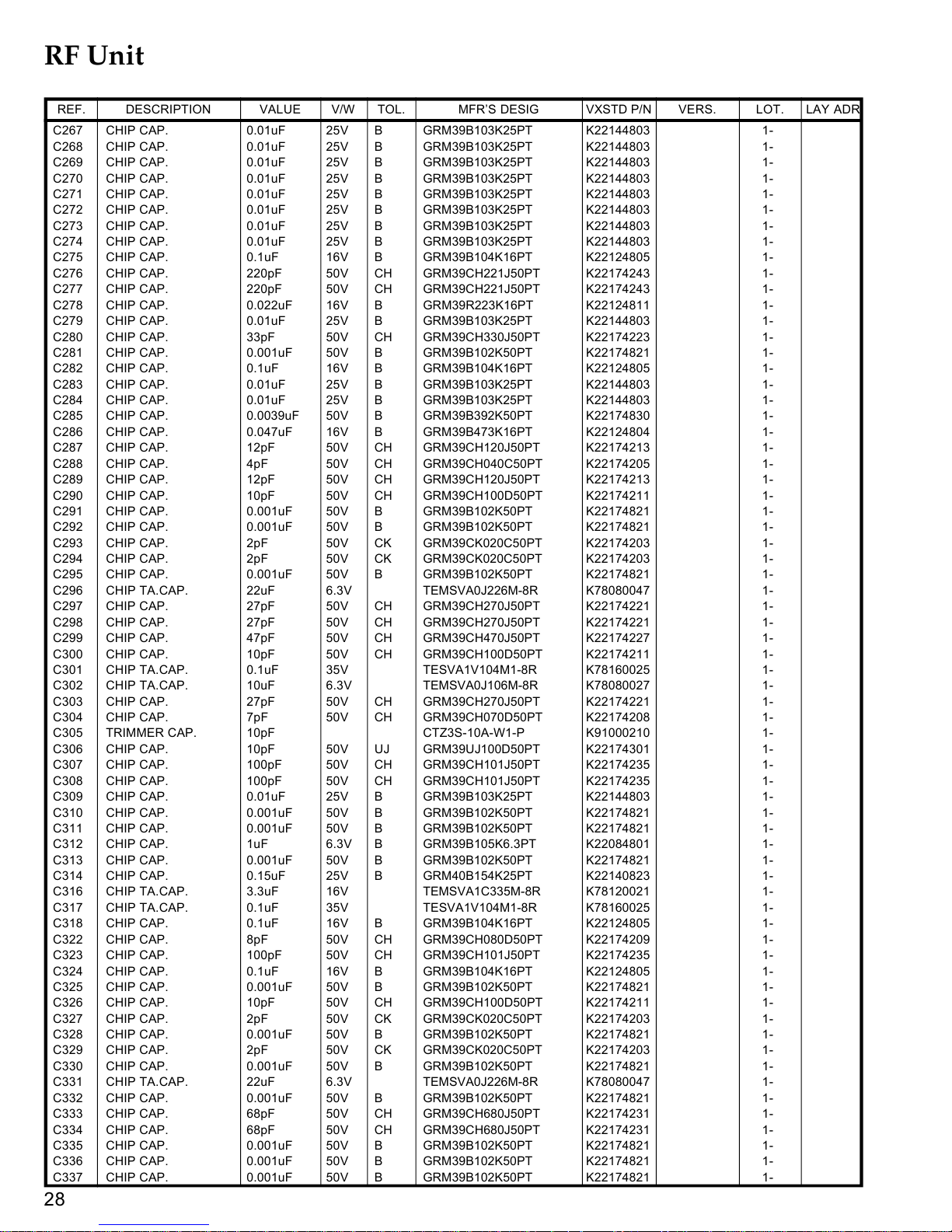
RF Unit
DESCRIPTION VALUE V/W TOL. VXSTD P/NMFR’S DESIG VERS.REF. LOT. LAY ADR
C267 CHIP CAP. 0.01uF 25V B GRM39B103K25PT K22144803 1-
C268 CHIP CAP. 0.01uF 25V B GRM39B103K25PT K22144803 1-
C269 CHIP CAP. 0.01uF 25V B GRM39B103K25PT K22144803 1-
C270 CHIP CAP. 0.01uF 25V B GRM39B103K25PT K22144803 1-
C271 CHIP CAP. 0.01uF 25V B GRM39B103K25PT K22144803 1-
C272 CHIP CAP. 0.01uF 25V B GRM39B103K25PT K22144803 1-
C273 CHIP CAP. 0.01uF 25V B GRM39B103K25PT K22144803 1-
C274 CHIP CAP. 0.01uF 25V B GRM39B103K25PT K22144803 1-
C275 CHIP CAP. 0.1uF 16V B GRM39B104K16PT K22124805 1-
C276 CHIP CAP. 220pF 50V CH GRM39CH221J50PT K22174243 1-
C277 CHIP CAP. 220pF 50V CH GRM39CH221J50PT K22174243 1-
C278 CHIP CAP. 0.022uF 16V B GRM39R223K16PT K22124811 1-
C279 CHIP CAP. 0.01uF 25V B GRM39B103K25PT K22144803 1-
C280 CHIP CAP. 33pF 50V CH GRM39CH330J50PT K22174223 1-
C281 CHIP CAP. 0.001uF 50V B GRM39B102K50PT K22174821 1-
C282 CHIP CAP. 0.1uF 16V B GRM39B104K16PT K22124805 1-
C283 CHIP CAP. 0.01uF 25V B GRM39B103K25PT K22144803 1-
C284 CHIP CAP. 0.01uF 25V B GRM39B103K25PT K22144803 1-
C285 CHIP CAP. 0.0039uF 50V B GRM39B392K50PT K22174830 1-
C286 CHIP CAP. 0.047uF 16V B GRM39B473K16PT K22124804 1-
C287 CHIP CAP. 12pF 50V CH GRM39CH120J50PT K22174213 1-
C288 CHIP CAP. 4pF 50V CH GRM39CH040C50PT K22174205 1-
C289 CHIP CAP. 12pF 50V CH GRM39CH120J50PT K22174213 1-
C290 CHIP CAP. 10pF 50V CH GRM39CH100D50PT K22174211 1-
C291 CHIP CAP. 0.001uF 50V B GRM39B102K50PT K22174821 1-
C292 CHIP CAP. 0.001uF 50V B GRM39B102K50PT K22174821 1-
C293 CHIP CAP. 2pF 50V CK GRM39CK020C50PT K22174203 1-
C294 CHIP CAP. 2pF 50V CK GRM39CK020C50PT K22174203 1-
C295 CHIP CAP. 0.001uF 50V B GRM39B102K50PT K22174821 1-
C296 CHIP TA.CAP. 22uF 6.3V TEMSVA0J226M-8R K78080047 1-
C297 CHIP CAP. 27pF 50V CH GRM39CH270J50PT K22174221 1-
C298 CHIP CAP. 27pF 50V CH GRM39CH270J50PT K22174221 1-
C299 CHIP CAP. 47pF 50V CH GRM39CH470J50PT K22174227 1-
C300 CHIP CAP. 10pF 50V CH GRM39CH100D50PT K22174211 1-
C301 CHIP TA.CAP. 0.1uF 35V TESVA1V104M1-8R K78160025 1-
C302 CHIP TA.CAP. 10uF 6.3V TEMSVA0J106M-8R K78080027 1-
C303 CHIP CAP. 27pF 50V CH GRM39CH270J50PT K22174221 1-
C304 CHIP CAP. 7pF 50V CH GRM39CH070D50PT K22174208 1-
C305 TRIMMER CAP. 10pF CTZ3S-10A-W1-P K91000210 1-
C306 CHIP CAP. 10pF 50V UJ GRM39UJ100D50PT K22174301 1-
C307 CHIP CAP. 100pF 50V CH GRM39CH101J50PT K22174235 1-
C308 CHIP CAP. 100pF 50V CH GRM39CH101J50PT K22174235 1-
C309 CHIP CAP. 0.01uF 25V B GRM39B103K25PT K22144803 1-
C310 CHIP CAP. 0.001uF 50V B GRM39B102K50PT K22174821 1-
C311 CHIP CAP. 0.001uF 50V B GRM39B102K50PT K22174821 1-
C312 CHIP CAP. 1uF 6.3V B GRM39B105K6.3PT K22084801 1-
C313 CHIP CAP. 0.001uF 50V B GRM39B102K50PT K22174821 1-
C314 CHIP CAP. 0.15uF 25V B GRM40B154K25PT K22140823 1-
C316 CHIP TA.CAP. 3.3uF 16V TEMSVA1C335M-8R K78120021 1-
C317 CHIP TA.CAP. 0.1uF 35V TESVA1V104M1-8R K78160025 1-
C318 CHIP CAP. 0.1uF 16V B GRM39B104K16PT K22124805 1-
C322 CHIP CAP. 8pF 50V CH GRM39CH080D50PT K22174209 1-
C323 CHIP CAP. 100pF 50V CH GRM39CH101J50PT K22174235 1-
C324 CHIP CAP. 0.1uF 16V B GRM39B104K16PT K22124805 1-
C325 CHIP CAP. 0.001uF 50V B GRM39B102K50PT K22174821 1-
C326 CHIP CAP. 10pF 50V CH GRM39CH100D50PT K22174211 1-
C327 CHIP CAP. 2pF 50V CK GRM39CK020C50PT K22174203 1-
C328 CHIP CAP. 0.001uF 50V B GRM39B102K50PT K22174821 1-
C329 CHIP CAP. 2pF 50V CK GRM39CK020C50PT K22174203 1-
C330 CHIP CAP. 0.001uF 50V B GRM39B102K50PT K22174821 1-
C331 CHIP TA.CAP. 22uF 6.3V TEMSVA0J226M-8R K78080047 1-
C332 CHIP CAP. 0.001uF 50V B GRM39B102K50PT K22174821 1-
C333 CHIP CAP. 68pF 50V CH GRM39CH680J50PT K22174231 1-
C334 CHIP CAP. 68pF 50V CH GRM39CH680J50PT K22174231 1-
C335 CHIP CAP. 0.001uF 50V B GRM39B102K50PT K22174821 1-
C336 CHIP CAP. 0.001uF 50V B GRM39B102K50PT K22174821 1-
C337 CHIP CAP. 0.001uF 50V B GRM39B102K50PT K22174821 1-
28
Page 29
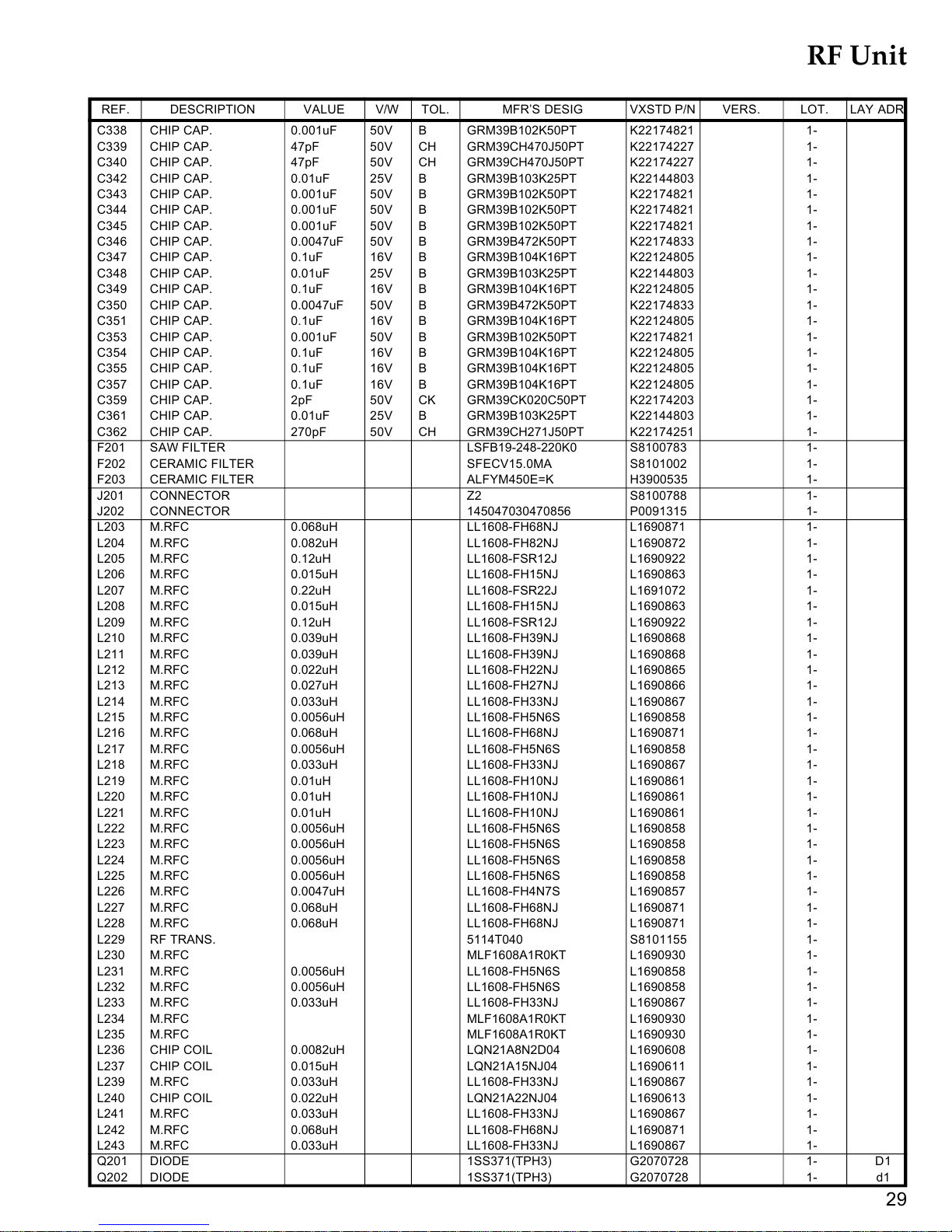
DESCRIPTION VALUE V/W TOL. VXSTD P/NMFR’S DESIG VERS.REF. LOT. LAY ADR
C338 CHIP CAP. 0.001uF 50V B GRM39B102K50PT K22174821 1-
C339 CHIP CAP. 47pF 50V CH GRM39CH470J50PT K22174227 1-
C340 CHIP CAP. 47pF 50V CH GRM39CH470J50PT K22174227 1-
C342 CHIP CAP. 0.01uF 25V B GRM39B103K25PT K22144803 1-
C343 CHIP CAP. 0.001uF 50V B GRM39B102K50PT K22174821 1-
C344 CHIP CAP. 0.001uF 50V B GRM39B102K50PT K22174821 1-
C345 CHIP CAP. 0.001uF 50V B GRM39B102K50PT K22174821 1-
C346 CHIP CAP. 0.0047uF 50V B GRM39B472K50PT K22174833 1-
C347 CHIP CAP. 0.1uF 16V B GRM39B104K16PT K22124805 1-
C348 CHIP CAP. 0.01uF 25V B GRM39B103K25PT K22144803 1-
C349 CHIP CAP. 0.1uF 16V B GRM39B104K16PT K22124805 1-
C350 CHIP CAP. 0.0047uF 50V B GRM39B472K50PT K22174833 1-
C351 CHIP CAP. 0.1uF 16V B GRM39B104K16PT K22124805 1-
C353 CHIP CAP. 0.001uF 50V B GRM39B102K50PT K22174821 1-
C354 CHIP CAP. 0.1uF 16V B GRM39B104K16PT K22124805 1-
C355 CHIP CAP. 0.1uF 16V B GRM39B104K16PT K22124805 1-
C357 CHIP CAP. 0.1uF 16V B GRM39B104K16PT K22124805 1-
C359 CHIP CAP. 2pF 50V CK GRM39CK020C50PT K22174203 1-
C361 CHIP CAP. 0.01uF 25V B GRM39B103K25PT K22144803 1-
C362 CHIP CAP. 270pF 50V CH GRM39CH271J50PT K22174251 1-
F201 SAW FILTER LSFB19-248-220K0 S8100783 1-
F202 CERAMIC FILTER SFECV15.0MA S8101002 1-
F203 CERAMIC FILTER ALFYM450E=K H3900535 1-
J201 CONNECTOR Z2 S8100788 1-
J202 CONNECTOR 145047030470856 P0091315 1-
L203 M.RFC 0.068uH LL1608-FH68NJ L1690871 1-
L204 M.RFC 0.082uH LL1608-FH82NJ L1690872 1-
L205 M.RFC 0.12uH LL1608-FSR12J L1690922 1-
L206 M.RFC 0.015uH LL1608-FH15NJ L1690863 1-
L207 M.RFC 0.22uH LL1608-FSR22J L1691072 1-
L208 M.RFC 0.015uH LL1608-FH15NJ L1690863 1-
L209 M.RFC 0.12uH LL1608-FSR12J L1690922 1-
L210 M.RFC 0.039uH LL1608-FH39NJ L1690868 1-
L211 M.RFC 0.039uH LL1608-FH39NJ L1690868 1-
L212 M.RFC 0.022uH LL1608-FH22NJ L1690865 1-
L213 M.RFC 0.027uH LL1608-FH27NJ L1690866 1-
L214 M.RFC 0.033uH LL1608-FH33NJ L1690867 1-
L215 M.RFC 0.0056uH LL1608-FH5N6S L1690858 1-
L216 M.RFC 0.068uH LL1608-FH68NJ L1690871 1-
L217 M.RFC 0.0056uH LL1608-FH5N6S L1690858 1-
L218 M.RFC 0.033uH LL1608-FH33NJ L1690867 1-
L219 M.RFC 0.01uH LL1608-FH10NJ L1690861 1-
L220 M.RFC 0.01uH LL1608-FH10NJ L1690861 1-
L221 M.RFC 0.01uH LL1608-FH10NJ L1690861 1-
L222 M.RFC 0.0056uH LL1608-FH5N6S L1690858 1-
L223 M.RFC 0.0056uH LL1608-FH5N6S L1690858 1-
L224 M.RFC 0.0056uH LL1608-FH5N6S L1690858 1-
L225 M.RFC 0.0056uH LL1608-FH5N6S L1690858 1-
L226 M.RFC 0.0047uH LL1608-FH4N7S L1690857 1-
L227 M.RFC 0.068uH LL1608-FH68NJ L1690871 1-
L228 M.RFC 0.068uH LL1608-FH68NJ L1690871 1-
L229 RF TRANS. 5114T040 S8101155 1-
L230 M.RFC MLF1608A1R0KT L1690930 1-
L231 M.RFC 0.0056uH LL1608-FH5N6S L1690858 1-
L232 M.RFC 0.0056uH LL1608-FH5N6S L1690858 1-
L233 M.RFC 0.033uH LL1608-FH33NJ L1690867 1-
L234 M.RFC MLF1608A1R0KT L1690930 1-
L235 M.RFC MLF1608A1R0KT L1690930 1-
L236 CHIP COIL 0.0082uH LQN21A8N2D04 L1690608 1-
L237 CHIP COIL 0.015uH LQN21A15NJ04 L1690611 1-
L239 M.RFC 0.033uH LL1608-FH33NJ L1690867 1-
L240 CHIP COIL 0.022uH LQN21A22NJ04 L1690613 1-
L241 M.RFC 0.033uH LL1608-FH33NJ L1690867 1-
L242 M.RFC 0.068uH LL1608-FH68NJ L1690871 1-
L243 M.RFC 0.033uH LL1608-FH33NJ L1690867 1-
Q201 DIODE 1SS371(TPH3) G2070728 1- D1
Q202 DIODE 1SS371(TPH3) G2070728 1- d1
RF Unit
29
Page 30
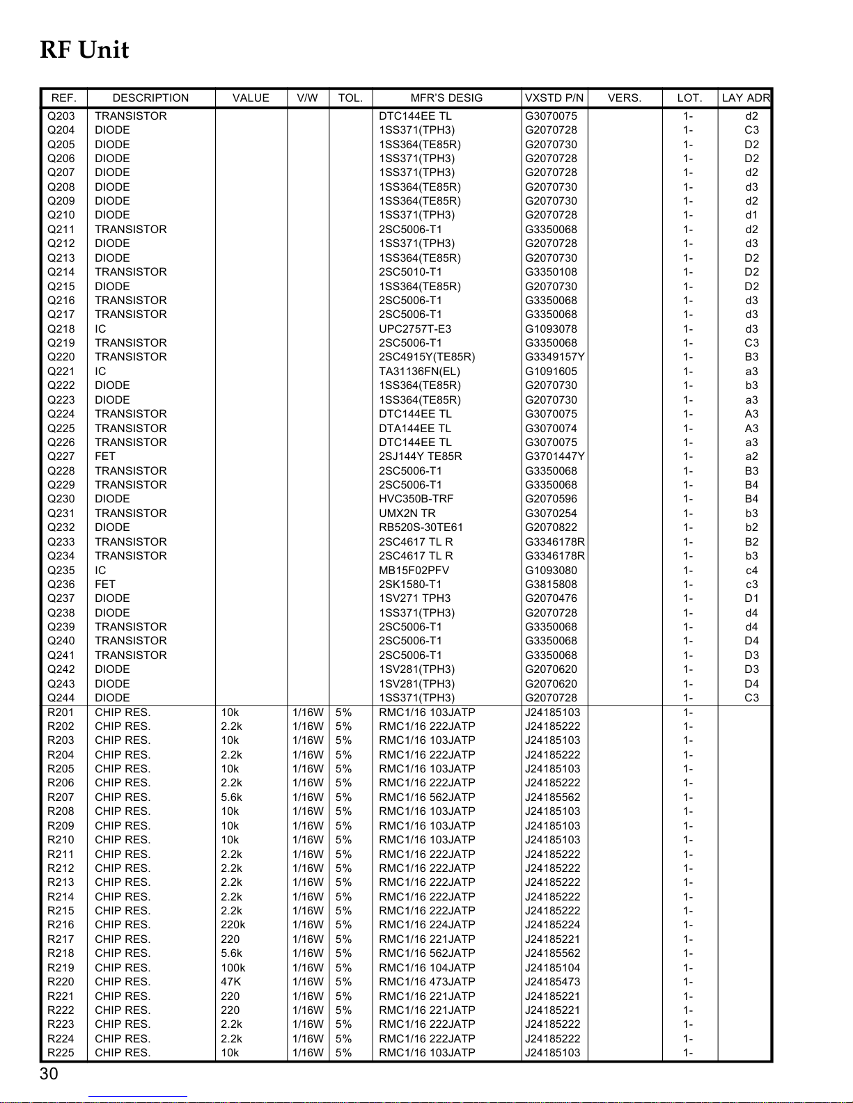
RF Unit
DESCRIPTION VALUE V/W TOL. VXSTD P/NMFR’S DESIG VERS.REF. LOT. LAY ADR
Q203 TRANSISTOR DTC144EE TL G3070075 1- d2
Q204 DIODE 1SS371(TPH3) G2070728 1- C3
Q205 DIODE 1SS364(TE85R) G2070730 1- D2
Q206 DIODE 1SS371(TPH3) G2070728 1- D2
Q207 DIODE 1SS371(TPH3) G2070728 1- d2
Q208 DIODE 1SS364(TE85R) G2070730 1- d3
Q209 DIODE 1SS364(TE85R) G2070730 1- d2
Q210 DIODE 1SS371(TPH3) G2070728 1- d1
Q211 TRANSISTOR 2SC5006-T1 G3350068 1- d2
Q212 DIODE 1SS371(TPH3) G2070728 1- d3
Q213 DIODE 1SS364(TE85R) G2070730 1- D2
Q214 TRANSISTOR 2SC5010-T1 G3350108 1- D2
Q215 DIODE 1SS364(TE85R) G2070730 1- D2
Q216 TRANSISTOR 2SC5006-T1 G3350068 1- d3
Q217 TRANSISTOR 2SC5006-T1 G3350068 1- d3
Q218 IC UPC2757T-E3 G1093078 1- d3
Q219 TRANSISTOR 2SC5006-T1 G3350068 1- C3
Q220 TRANSISTOR 2SC4915Y(TE85R) G3349157Y 1- B3
Q221 IC TA31136FN(EL) G1091605 1- a3
Q222 DIODE 1SS364(TE85R) G2070730 1- b3
Q223 DIODE 1SS364(TE85R) G2070730 1- a3
Q224 TRANSISTOR DTC144EE TL G3070075 1- A3
Q225 TRANSISTOR DTA144EE TL G3070074 1- A3
Q226 TRANSISTOR DTC144EE TL G3070075 1- a3
Q227 FET 2SJ144Y TE85R G3701447Y 1- a2
Q228 TRANSISTOR 2SC5006-T1 G3350068 1- B3
Q229 TRANSISTOR 2SC5006-T1 G3350068 1- B4
Q230 DIODE HVC350B-TRF G2070596 1- B4
Q231 TRANSISTOR UMX2N TR G3070254 1- b3
Q232 DIODE RB520S-30TE61 G2070822 1- b2
Q233 TRANSISTOR 2SC4617 TL R G3346178R 1- B2
Q234 TRANSISTOR 2SC4617 TL R G3346178R 1- b3
Q235 IC MB15F02PFV G1093080 1- c4
Q236 FET 2SK1580-T1 G3815808 1- c3
Q237 DIODE 1SV271 TPH3 G2070476 1- D1
Q238 DIODE 1SS371(TPH3) G2070728 1- d4
Q239 TRANSISTOR 2SC5006-T1 G3350068 1- d4
Q240 TRANSISTOR 2SC5006-T1 G3350068 1- D4
Q241 TRANSISTOR 2SC5006-T1 G3350068 1- D3
Q242 DIODE 1SV281(TPH3) G2070620 1- D3
Q243 DIODE 1SV281(TPH3) G2070620 1- D4
Q244 DIODE 1SS371(TPH3) G2070728 1- C3
R201 CHIP RES. 10k 1/16W 5% RMC1/16 103JATP J24185103 1-
R202 CHIP RES. 2.2k 1/16W 5% RMC1/16 222JATP J24185222 1-
R203 CHIP RES. 10k 1/16W 5% RMC1/16 103JATP J24185103 1-
R204 CHIP RES. 2.2k 1/16W 5% RMC1/16 222JATP J24185222 1-
R205 CHIP RES. 10k 1/16W 5% RMC1/16 103JATP J24185103 1-
R206 CHIP RES. 2.2k 1/16W 5% RMC1/16 222JATP J24185222 1-
R207 CHIP RES. 5.6k 1/16W 5% RMC1/16 562JATP J24185562 1-
R208 CHIP RES. 10k 1/16W 5% RMC1/16 103JATP J24185103 1-
R209 CHIP RES. 10k 1/16W 5% RMC1/16 103JATP J24185103 1-
R210 CHIP RES. 10k 1/16W 5% RMC1/16 103JATP J24185103 1-
R211 CHIP RES. 2.2k 1/16W 5% RMC1/16 222JATP J24185222 1-
R212 CHIP RES. 2.2k 1/16W 5% RMC1/16 222JATP J24185222 1-
R213 CHIP RES. 2.2k 1/16W 5% RMC1/16 222JATP J24185222 1-
R214 CHIP RES. 2.2k 1/16W 5% RMC1/16 222JATP J24185222 1-
R215 CHIP RES. 2.2k 1/16W 5% RMC1/16 222JATP J24185222 1-
R216 CHIP RES. 220k 1/16W 5% RMC1/16 224JATP J24185224 1-
R217 CHIP RES. 220 1/16W 5% RMC1/16 221JATP J24185221 1-
R218 CHIP RES. 5.6k 1/16W 5% RMC1/16 562JATP J24185562 1-
R219 CHIP RES. 100k 1/16W 5% RMC1/16 104JATP J24185104 1-
R220 CHIP RES. 47K 1/16W 5% RMC1/16 473JATP J24185473 1-
R221 CHIP RES. 220 1/16W 5% RMC1/16 221JATP J24185221 1-
R222 CHIP RES. 220 1/16W 5% RMC1/16 221JATP J24185221 1-
R223 CHIP RES. 2.2k 1/16W 5% RMC1/16 222JATP J24185222 1-
R224 CHIP RES. 2.2k 1/16W 5% RMC1/16 222JATP J24185222 1-
R225 CHIP RES. 10k 1/16W 5% RMC1/16 103JATP J24185103 1-
30
Page 31
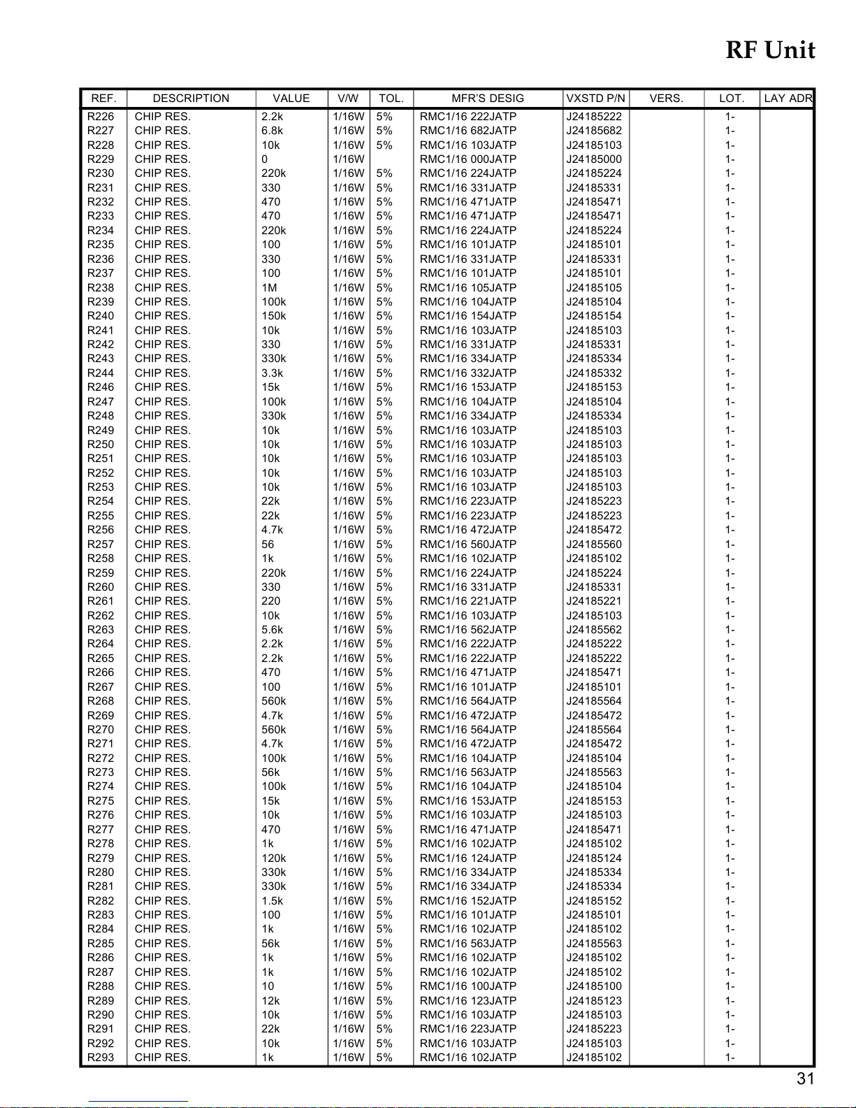
DESCRIPTION VALUE V/W TOL. VXSTD P/NMFR’S DESIG VERS.REF. LOT. LAY ADR
R226 CHIP RES. 2.2k 1/16W 5% RMC1/16 222JATP J24185222 1-
R227 CHIP RES. 6.8k 1/16W 5% RMC1/16 682JATP J24185682 1-
R228 CHIP RES. 10k 1/16W 5% RMC1/16 103JATP J24185103 1-
R229 CHIP RES. 0 1/16W RMC1/16 000JATP J24185000 1-
R230 CHIP RES. 220k 1/16W 5% RMC1/16 224JATP J24185224 1-
R231 CHIP RES. 330 1/16W 5% RMC1/16 331JATP J24185331 1-
R232 CHIP RES. 470 1/16W 5% RMC1/16 471JATP J24185471 1-
R233 CHIP RES. 470 1/16W 5% RMC1/16 471JATP J24185471 1-
R234 CHIP RES. 220k 1/16W 5% RMC1/16 224JATP J24185224 1-
R235 CHIP RES. 100 1/16W 5% RMC1/16 101JATP J24185101 1-
R236 CHIP RES. 330 1/16W 5% RMC1/16 331JATP J24185331 1-
R237 CHIP RES. 100 1/16W 5% RMC1/16 101JATP J24185101 1-
R238 CHIP RES. 1M 1/16W 5% RMC1/16 105JATP J24185105 1-
R239 CHIP RES. 100k 1/16W 5% RMC1/16 104JATP J24185104 1-
R240 CHIP RES. 150k 1/16W 5% RMC1/16 154JATP J24185154 1-
R241 CHIP RES. 10k 1/16W 5% RMC1/16 103JATP J24185103 1-
R242 CHIP RES. 330 1/16W 5% RMC1/16 331JATP J24185331 1-
R243 CHIP RES. 330k 1/16W 5% RMC1/16 334JATP J24185334 1-
R244 CHIP RES. 3.3k 1/16W 5% RMC1/16 332JATP J24185332 1-
R246 CHIP RES. 15k 1/16W 5% RMC1/16 153JATP J24185153 1-
R247 CHIP RES. 100k 1/16W 5% RMC1/16 104JATP J24185104 1-
R248 CHIP RES. 330k 1/16W 5% RMC1/16 334JATP J24185334 1-
R249 CHIP RES. 10k 1/16W 5% RMC1/16 103JATP J24185103 1-
R250 CHIP RES. 10k 1/16W 5% RMC1/16 103JATP J24185103 1-
R251 CHIP RES. 10k 1/16W 5% RMC1/16 103JATP J24185103 1-
R252 CHIP RES. 10k 1/16W 5% RMC1/16 103JATP J24185103 1-
R253 CHIP RES. 10k 1/16W 5% RMC1/16 103JATP J24185103 1-
R254 CHIP RES. 22k 1/16W 5% RMC1/16 223JATP J24185223 1-
R255 CHIP RES. 22k 1/16W 5% RMC1/16 223JATP J24185223 1-
R256 CHIP RES. 4.7k 1/16W 5% RMC1/16 472JATP J24185472 1-
R257 CHIP RES. 56 1/16W 5% RMC1/16 560JATP J24185560 1-
R258 CHIP RES. 1k 1/16W 5% RMC1/16 102JATP J24185102 1-
R259 CHIP RES. 220k 1/16W 5% RMC1/16 224JATP J24185224 1-
R260 CHIP RES. 330 1/16W 5% RMC1/16 331JATP J24185331 1-
R261 CHIP RES. 220 1/16W 5% RMC1/16 221JATP J24185221 1-
R262 CHIP RES. 10k 1/16W 5% RMC1/16 103JATP J24185103 1-
R263 CHIP RES. 5.6k 1/16W 5% RMC1/16 562JATP J24185562 1-
R264 CHIP RES. 2.2k 1/16W 5% RMC1/16 222JATP J24185222 1-
R265 CHIP RES. 2.2k 1/16W 5% RMC1/16 222JATP J24185222 1-
R266 CHIP RES. 470 1/16W 5% RMC1/16 471JATP J24185471 1-
R267 CHIP RES. 100 1/16W 5% RMC1/16 101JATP J24185101 1-
R268 CHIP RES. 560k 1/16W 5% RMC1/16 564JATP J24185564 1-
R269 CHIP RES. 4.7k 1/16W 5% RMC1/16 472JATP J24185472 1-
R270 CHIP RES. 560k 1/16W 5% RMC1/16 564JATP J24185564 1-
R271 CHIP RES. 4.7k 1/16W 5% RMC1/16 472JATP J24185472 1-
R272 CHIP RES. 100k 1/16W 5% RMC1/16 104JATP J24185104 1-
R273 CHIP RES. 56k 1/16W 5% RMC1/16 563JATP J24185563 1-
R274 CHIP RES. 100k 1/16W 5% RMC1/16 104JATP J24185104 1-
R275 CHIP RES. 15k 1/16W 5% RMC1/16 153JATP J24185153 1-
R276 CHIP RES. 10k 1/16W 5% RMC1/16 103JATP J24185103 1-
R277 CHIP RES. 470 1/16W 5% RMC1/16 471JATP J24185471 1-
R278 CHIP RES. 1k 1/16W 5% RMC1/16 102JATP J24185102 1-
R279 CHIP RES. 120k 1/16W 5% RMC1/16 124JATP J24185124 1-
R280 CHIP RES. 330k 1/16W 5% RMC1/16 334JATP J24185334 1-
R281 CHIP RES. 330k 1/16W 5% RMC1/16 334JATP J24185334 1-
R282 CHIP RES. 1.5k 1/16W 5% RMC1/16 152JATP J24185152 1-
R283 CHIP RES. 100 1/16W 5% RMC1/16 101JATP J24185101 1-
R284 CHIP RES. 1k 1/16W 5% RMC1/16 102JATP J24185102 1-
R285 CHIP RES. 56k 1/16W 5% RMC1/16 563JATP J24185563 1-
R286 CHIP RES. 1k 1/16W 5% RMC1/16 102JATP J24185102 1-
R287 CHIP RES. 1k 1/16W 5% RMC1/16 102JATP J24185102 1-
R288 CHIP RES. 10 1/16W 5% RMC1/16 100JATP J24185100 1-
R289 CHIP RES. 12k 1/16W 5% RMC1/16 123JATP J24185123 1-
R290 CHIP RES. 10k 1/16W 5% RMC1/16 103JATP J24185103 1-
R291 CHIP RES. 22k 1/16W 5% RMC1/16 223JATP J24185223 1-
R292 CHIP RES. 10k 1/16W 5% RMC1/16 103JATP J24185103 1-
R293 CHIP RES. 1k 1/16W 5% RMC1/16 102JATP J24185102 1-
RF Unit
31
Page 32
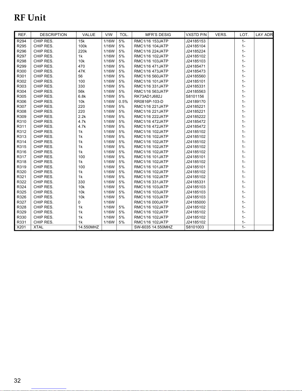
RF Unit
DESCRIPTION VALUE V/W TOL. VXSTD P/NMFR’S DESIG VERS.REF. LOT. LAY ADR
R294 CHIP RES. 15k 1/16W 5% RMC1/16 153JATP J24185153 1-
R295 CHIP RES. 100k 1/16W 5% RMC1/16 104JATP J24185104 1-
R296 CHIP RES. 220k 1/16W 5% RMC1/16 224JATP J24185224 1-
R297 CHIP RES. 1k 1/16W 5% RMC1/16 102JATP J24185102 1-
R298 CHIP RES. 10k 1/16W 5% RMC1/16 103JATP J24185103 1-
R299 CHIP RES. 470 1/16W 5% RMC1/16 471JATP J24185471 1-
R300 CHIP RES. 47K 1/16W 5% RMC1/16 473JATP J24185473 1-
R301 CHIP RES. 56 1/16W 5% RMC1/16 560JATP J24185560 1-
R302 CHIP RES. 100 1/16W 5% RMC1/16 101JATP J24185101 1-
R303 CHIP RES. 330 1/16W 5% RMC1/16 331JATP J24185331 1-
R304 CHIP RES. 56k 1/16W 5% RMC1/16 563JATP J24185563 1-
R305 CHIP RES. 6.8k 1/16W 5% RK73AD1J682J S8101156 1-
R306 CHIP RES. 10k 1/16W 0.5% RR0816P-103-D J24189170 1-
R307 CHIP RES. 220 1/16W 5% RMC1/16 221JATP J24185221 1-
R308 CHIP RES. 220 1/16W 5% RMC1/16 221JATP J24185221 1-
R309 CHIP RES. 2.2k 1/16W 5% RMC1/16 222JATP J24185222 1-
R310 CHIP RES. 4.7k 1/16W 5% RMC1/16 472JATP J24185472 1-
R311 CHIP RES. 4.7k 1/16W 5% RMC1/16 472JATP J24185472 1-
R312 CHIP RES. 1k 1/16W 5% RMC1/16 102JATP J24185102 1-
R313 CHIP RES. 1k 1/16W 5% RMC1/16 102JATP J24185102 1-
R314 CHIP RES. 1k 1/16W 5% RMC1/16 102JATP J24185102 1-
R315 CHIP RES. 1k 1/16W 5% RMC1/16 102JATP J24185102 1-
R316 CHIP RES. 1k 1/16W 5% RMC1/16 102JATP J24185102 1-
R317 CHIP RES. 100 1/16W 5% RMC1/16 101JATP J24185101 1-
R318 CHIP RES. 1k 1/16W 5% RMC1/16 102JATP J24185102 1-
R319 CHIP RES. 100 1/16W 5% RMC1/16 101JATP J24185101 1-
R320 CHIP RES. 1k 1/16W 5% RMC1/16 102JATP J24185102 1-
R321 CHIP RES. 1k 1/16W 5% RMC1/16 102JATP J24185102 1-
R322 CHIP RES. 330 1/16W 5% RMC1/16 331JATP J24185331 1-
R324 CHIP RES. 10k 1/16W 5% RMC1/16 103JATP J24185103 1-
R325 CHIP RES. 10k 1/16W 5% RMC1/16 103JATP J24185103 1-
R326 CHIP RES. 10k 1/16W 5% RMC1/16 103JATP J24185103 1-
R327 CHIP RES. 0 1/16W RMC1/16 000JATP J24185000 1-
R328 CHIP RES. 1k 1/16W 5% RMC1/16 102JATP J24185102 1-
R329 CHIP RES. 1k 1/16W 5% RMC1/16 102JATP J24185102 1-
R330 CHIP RES. 1k 1/16W 5% RMC1/16 102JATP J24185102 1-
R331 CHIP RES. 1k 1/16W 5% RMC1/16 102JATP J24185102 1-
X201 XTAL 14.550MHZ SW-6035 14.550MHZ S8101003 1-
32
Page 33

RF Unit
33
Page 34

RF Unit
Copyright © 2002
VERTEX STANDARD CO., LTD.
All rights reserved
34
No portion of this manual may be
reproduced without the permission
of VERTEX STANDARD CO., LTD.
Printed in Japan.
 Loading...