

Page 1
0
R
DS029 (v1.3) June 25, 2000
02
XQ4000X Series Features
• Certified to MIL-PRF-38535 Appendix A QML
(Qualified Manufacturer Listing)
• Ceramic and plastic packages
• Also available under the following standard microcircuit
drawings (SMD)
- XQ4013XL 5962-98513
- XQ4036XL 5962-98510
- XQ4062XL 5962-98511
- XQ4085XL 5962-99575
• For more information contact the Defense Supply
Center Columbus (DSCC)
http://www.dscc.dla.mis/v/va/smd/smdsrch.html
• Available in -3 speed
• System featured Field-Programmable Gate Arrays
- SelectRAM™ memory: on-chip ultra-fast RAM with
· synchronous write option
· dual-port RAM option
- Abundant flip-flops
- Flexible function generators
- Dedicated high-speed carry logic
- Wide edge decoders on each edge
- Hierarchy of interconnect lines
- Internal 3-state bus capability
- Eight global low-skew clock or signal distribution
networks
• System performance beyond 50 MHz
• Flexible array architec t u re
• Low power segmented routing architecture
• Systems-oriented features
- IEEE 1149.1-compatible boundary scan logic
support
- Individually programmable output slew rate
- Programmable input pull-up or pull-down resistors
- 12 mA sink current per XQ4000XL output
• Configured by loading binary file
- Unlimited reprogrammability
• Readback capability
- Program verification
- Internal node observability
QPRO XQ4000XL Series QML
High-Reliability FPGAs
Produc t S pecif i catio n
• Development system runs on most common computer
platforms
- Interfaces to popular design environments
- Fully automatic mapping , placement and ro uting
- Interactive design editor for design optimization
• Highest capacity—over 180,000 usable gates
• Additional routing over XQ4000E
- Almost twice the routing capacity for high-density
designs
• Buffered Interconnect for maximum speed
• New latch capability in configurable logic blocks
• Improved VersaRing™ I/O interconnect for better Fix ed
pinout flexibility
- Virtually unlimited number of clock signals
• Optional multiplexer or 2-input function generator on
device outputs
• 5V tolerant I/Os
• 0.35 µm SRAM process
Introduction
The QPRO™ XQ4000XL Series high-performance,
high-capacity Field Programmable Gate Arrays (FPGAs)
provide the benefits of custom CMOS VLSI, while avoiding
the initial cost, long development cycle, and inherent risk of
a conventional masked gate array.
The result of thirteen years of FPGA design experience and
feedback from thousands of customers, these FPGAs combine architectural versatility, on-chip Select-RAM memor y
with edge-triggered and dual-port modes, increased speed,
abundant routing resources, and new, sophisticated
soft-ware to achieve fully automated implementation of
complex, high-density, high-performance designs.
Refer to the complete Commercial XC 4000XL Se ries Field
Programmable Gate Arrays Data Sheet for more information on device architecture and timing, and the latest Xilinx
databook for package pinouts other than the CB228
(included in this data sheet). (Pinouts for XQ4000XL device
are identical to XC4000XL.)
© 2000 Xilinx, Inc. All rights reserved. All Xilinx trademarks, registered trademarks, patents, and disclaimers are as listed at http://www.xilinx.com/legal.htm.
All other trademarks and registered trademarks are the property of their respective owners. All specifications are subject to change without notice.
DS029 (v1.3) June 25, 2000 www.xilinx.com 1
Product Specification 1-800-255-7778
Page 2
QPR O XQ4000X L Seri es QML High-Rel iabi l i ty FPGA s
Table 1: XQ4000XL Series High Reliability Field Progammable Gate Arrays
Max
Device
Logic
Cells
Logic
Gates
(No
RAM)
(1)
Max.
RAM
Bits (No
Logic)
Typical Gate
Range
(Logic and
(1)
RAM)
CLB
Matrix
Total
CLBs
Number
of
Flip-Flops
Max.
User
I/O Packages
XQ4013XL 2432 13,000 18,43 2 10,000-30,000 24x24 576 1,536 192 PG223, CB228,
PQ240, BG256
XQ4036XL 3078 36,000 4 1,472 22,000-65,000 36x36 1,296 3,168 288 PG411, CB228,
HQ240, BG352
XQ4062XL 5472 62,000 7 3,728 40,000-130,000 48x48 2, 304 5,376 384 PG475, CB228,
HQ240, BG432
XQ4085XL 7448 85,000 100,352 55,000-180,000 56x56 3,136 7,168 448 PG475, CB228,
HQ240, BG432
Notes:
1. Maximum val ues of typical gate range includes 20% to 30% of CLBs used as RAM.
R
2 www.xilinx.com DS029 (v1.3) June 25, 2000
1-800-255-7778 Product Specification
Page 3
R
QPRO XQ4000XL Series QML High-Reliability FPGAs
XQ4000XL Switching Characteristics
Definition of Terms
In the following tables, some specifications may be designated as Advance or Preliminary. These ter ms are defined as
follows:
Advance: Initial estimates based on simulation and/or extrapolation from other speed grades, devices, or
devicefamilies. Values are subject to change. Use as estimates, not for production.
Preliminary: Based on preliminary characterization. Further changes are not expected.
Unmarked: Specifications not identified as either Advance or Preliminary are to be considered Final.
Except for pin-to-pin input and output parameters, the a.c. parameter delay specifications included in this documen t are
derived from measuring internal test patterns. All specifications are representative of worst-case supply voltage and junction
temperature conditions.
All specifications subject to change without notice.
Additio nal Specif icati ons
Except for pin-to-pin input and output parameters, the a.c.
parameter delay specifications included in this document
are derived from measuring internal test patterns. All specifications are representative of worst-case supply voltage
and junction temperature conditions. The parameters
included are common to popular designs and typical appli-
Absolute Maximum Ratings
(1)
cations. For design considerations requiring more detailed
timing information, se e the appropriate family AC supplements available on the Xilinx web site at:
http://www.xilinx.com/partinfo/databook.htm
.
Symbol Description Units
V
V
T
T
V
V
CCt
STG
SOL
T
CC
IN
TS
J
Supply voltage relative to GND –0.5 to 4.0 V
Input voltage relative to GND
Voltage applied to High-Z output
(2)
(2)
–0.5 to 5.5 V
–0.5 to 5.5 V
Longest supply voltage rise time from 1V to 3V 50 ms
Storage temperature (ambient) –65 to +150 °C
Maximum soldering temperature (10s @ 1/16 in. = 1.5 mm) +260 °C
Junction temperature Ceramic package +150 °C
Plastic package +125 °C
Notes:
1. Stresses beyond those listed under Absolute Maximum Ratings may cause permanent damage to the device. These are stress
ratings onl y, and functional operat ion of the device at these or any other condition s beyond those listed under Operating Conditions
is not implied. Exposure to Absolute Maximum Ratings conditions for extended periods of time may affec t device reliab il ity.
2. Maximum DC over shoot or undershoot above V
achieve. During transitions, the device pins may undershoot to –2. 0 V or over shoot to VCC + 2.0V, pro vided this over- or undershoot
lasts less than 10 ns and with the forcing current being limited to 200 mA.
Recommended Operating Conditions
or below GND must be limited to either 0.5V or 10 mA, whichever is easier to
CC
(1)
Symbol Description Min Max Units
V
CC
V
V
T
Notes:
1. At junction temperatures abov e those listed as Operating Conditions, all delay param eters increase by 0.35% per °C.
2. Input and output measurement threshold is ~50% of V
Supply voltage relative to GND, TJ = –55°C to +125°CPlastic 3.0 3.6 V
Supply voltage relative to GND, T
High-level input voltage
IH
Low-level input vol tage 0 30% of V
IL
Input signal transition time - 250 ns
IN
(2)
= –55°C to +125°C Ceramic 3.0 3.6 V
C
CC
50% of V
.
CC
5.5 V
CC
V
DS029 (v1.3) June 25, 2000 www.xilinx.com 3
Product Specification 1-800-255-7778
Page 4
QPR O XQ4000X L Series QML High-Reliability FPGAs
XQ4000XL DC Characteristics Over Recommended Operating Conditions
Symbol Description Min Max Units
R
V
OH
V
V
I
CCO
I
C
OL
DR
L
IN
High-level output voltage at IOH = –4 mA, VCC min (LVTTL) 2.4 - V
High-level output voltage at I
Low-lev el output voltage at IOL = 12 mA, VCC min (LVTTL)
Low-lev el output voltage at I
= –500 µA, (LVCMOS) 90% V
OH
(1)
= 1500 µA, (LVCMOS) - 10% V
OL
CC
-0.4V
Data retention supply voltage (below which configuration data may be lost) 2.5 - V
Quiescent FPGA supply current
(2)
-5mA
Input or output leakage current –10 +10 µA
Input capacitance (sample tested) BGA, PQ, HQ, packages - 10 pF
PGA packages - 16 pF
I
RPU
I
RPD
I
RLL
Notes:
1. With up to 64 pins simul taneously sinking 12 mA.
2. With no output current l oads, no active input or Longline pull- up resistors, all I/O pins in a High-Z state and floating.
Pad pull-up (when selected) at VIN = 0V (sample tested) 0.02 0.25 mA
Pad pull-down (when selected) at VIN = 3.6V (sample tested) 0.02 0.15 mA
Horizontal longline pull-up (when selected) at logic Low 0.3 2.0 mA
Power-On Power Supply Requirements
Xilinx FPGAs require a minimum rated power supply current
capacity to insure proper initialization, and the power supply
ramp-up time does affect the current required. A fast
ramp-up time requires more current than a slow ramp-up
time. The slowest ramp-up time is 50 ms. Current capacity
is not specified for a ramp-up time faster than 2 ms. The cur-
rent capacity varies linealy with ramp-up time, e.g., an
XQ4036XL with a ramp-up time of 25 ms would require a
capacity predicted by the po int on the straight line drawn
from 1A at 120 µs to 500 mA at 50 ms at the 25 ms time
mark. This point is approximately 750 mA
-V
CC
.
V
Ramp-up Time
Product Descrip t ion
Fast (120 µs) Slow (50 ms)
XQ4013 - 36XL Minimum required current supply 1A 500 mA
XC4062XL Minimum required curre nt supply 2A 500 mA
XC4085XL
Notes:
1. The XC4085XL fast r am p-up time is 5 ms.
2. Devices ar e guaranteed to initialize properly with the minimum current listed above. A larger capacity power supply may result in a
large r initialization current.
3. This specification applies to Commercial and Industrial grade products only.
4. Ramp-up Time is measured from 0V
on reset threshold voltage . After initialization and before configuration, I
(1)
Minimum required current supply 2A
to 3.6VDC. Peak current required lasts less than 3 ms, and occurs near the internal power
DC
max is less than 10 mA.
CC
(1)
500 mA
4 www.xilinx.com DS029 (v1.3) June 25, 2000
1-800-255-7778 Product Specification
Page 5
R
XQ4000XL AC Switching Characteristic
QPRO XQ4000XL Series QML High-Reliability FPGAs
Testing of the switching parameters is modeled after testing
methods specified by MIL-M-38510/605. All devices are
100% functionally tested. Internal timing parameters are
derived from measuri ng i nter n al t est patter ns. Listed below
are representative values where one global clock input
drives one vertical clock line in each acc essible column, and
where all accessible IOB and CLB flip-flops are c locked by
the global clock net.
When fewer vertical clock lines are connected, the clock dis-
driven from the same gl obal clock, the delay is longer. For
more specific, more precise, and worst-case guaranteed
data, reflecting the actual routing str ucture, use the values
provided by the static timing analyzer (TRCE in the Xilinx
Development System) and back-annotated to the simulation
netlist. These path delays, provided as a guideline, have
been extracted from the static timing analyzer report. All
timing parameters assume worst-case operating conditions
(supply voltage and junction temperature)
tribution is faster; when multiple clock lines per column are
Global Buffer Switching Characteristics
Symbol Description Device
T
GLS
Delay from pad through Global Low Skew buffer, to any
clo ck K
XQ4013XL 0.6 3.6 - ns
XQ4036XL 1.1 4.8 - ns
XQ4062XL 1.4 6.3 - ns
XQ4085XL 1.6 - 5.7 ns
Global Early BUFGEs 1, 2, 5, and 6 to IOB Clock Characteristics
All
Min
-3 -1
UnitsMax Max
Symbol Description Device
T
GE
Delay from pad through Global Early buffer, to any IOB
clock. Values are for BUFGEs 1, 2, 5 and 6.
XQ4013XL 0.4 2.4 - ns
XQ4036XL 0.3 3.1 - ns
XQ4062XL 0.3 4.9 - ns
XQ4085XL 0.4 - 4.7 ns
Global Early BUFGEs 3, 4, 7, and 8 to IOB Clock Characteristics
Symbol Description Device
T
GE
Delay from pad through Global Early buffer, to any IOB
clock. Values are for BUFGEs 3, 4, 7 and 8.
XQ4013XL 0.7 2.4 - ns
XQ4036XL 0.9 4.7 - ns
XQ4062XL 1.2 5.9 - ns
XQ4085XL 1.3 - 5.5 ns
All
Min
All
Min
-3 -1
UnitsMax Max
-3 -1
UnitsMax Max
DS029 (v1.3) June 25, 2000 www.xilinx.com 5
Product Specification 1-800-255-7778
Page 6

QPR O XQ4000X L Series QML High-Reliability FPGAs
XQ4000XL CLB Switching Characteristic Guidelines
Testing of switching parameters is modeled after testing
methods specified by MIL-M-38510/605. All devices are
100% functionally tested. Internal timing parameters are
derived from measuri ng i nter n al t est patter ns. Listed below
are representative values. For mo re specific, more precise,
and worst-case guaranteed data, use t he values reported
by the static timing analyzer (TRCE in the Xilinx Development System) an d back-ann otated to th e simu lation n etlist.
All timing parameters ass ume worst-case operating con ditions (supply voltage and junction temperature). Values
apply to all XQ4000XL devices and expressed in nanos econds unless otherwise noted.
CLB Switching Characteristics
Symbol Description
Combinatorial Delays
T
ILO
T
IHO
T
ITO
T
HH0O
T
HH1O
T
HH2O
T
CBYP
CLB Fast Carry Logic
T
OPCY
T
ASCY
T
INCY
T
SUM
T
BYP
T
NET
Sequential Delays
T
CKO
T
CKLO
Setup Time Before Clock K
T
ICK
T
IHCK
T
HH0CK
T
HH1CK
T
HH2CK
T
DICK
T
ECCK
T
RCK
T
CCK
T
CHCK
F/G inputs to X/Y outputs - 1.6 - 1.3 ns
F/G inputs vi a H ’ to X/Y outputs - 2.7 - 2.2 ns
F/G inputs via transparent latch to Q outputs - 2.9 - 2.2 ns
C inputs via SR/H0 via H to X/Y outputs - 2.5 - 2.0 ns
C inputs via H1 via H to X/Y outputs - 2.4 - 1.9 ns
C inputs via DIN/H2 via H to X/Y outputs - 2 .5 - 2.0 ns
C inputs via EC, DIN/H2 to YQ, XQ output (bypass) - 1.5 - 1.1 ns
Operand inputs (F1, F2, G1, G4) to C
Add/subtract input (F3) to C
OUT
Initialization inputs (F1, F3) to C
OUT
OUT
CIN through function generators to X/Y outputs - 2.8 - 2.4 ns
C
to C
IN
Carry net delay, C
, bypass function generators - 0.26 - 0.20 ns
OUT
to C
OUT
IN
Clock K to flip-flop outputs Q - 2.1 - 1.6 ns
Clock K to latch outputs Q - 2.1 - 1.6 ns
F/G inputs 1.1 - 0.9 - ns
F/G in puts via H 2.2 - 1.7 - ns
C inputs via H0 through H 2.0 - 1.6 - ns
C inputs via H1 through H 1.9 - 1.4 - ns
C inputs via H2 through H 2.0 - 1.6 - ns
C inputs via D
IN
C inputs via EC 1.0 - 0.8 - ns
C inputs via S/R, going Low (inactive) 0.6 - 0.5 - ns
CIN input via F/G 2.3 - 1.9 - ns
CIN input via F/G and H 3.4 - 2.7 - ns
R
-3 -1
UnitsMin Max Min Max
-2.7-2.0ns
-3.3-2.5ns
-2.0-1.5ns
- 0.32 - 0.25 ns
0.9 - 0.7 - ns
6 www.xilinx.com DS029 (v1.3) June 25, 2000
1-800-255-7778 Product Specification
Page 7
R
CLB Switching Characteristics (Continued)
Symbol Description
Hold Time After Clock K
T
CKI
T
CKIH
T
CKHH0
T
CKHH1
T
CKHH2
T
CKDI
T
CKEC
T
CKR
Clock
T
CH
T
CL
Set/Reset Direct
T
RPW
T
RIO
Global Set/Reset
T
MRW
T
MRQ
F
TOG
F/G inputs 0 - 0 - ns
F/G inputs vi a H 0 - 0 - ns
C inputs via SR/H0 through H 0 - 0 - ns
C inputs via H1 through H 0 - 0 - ns
C inputs via DIN/H2 through H 0 - 0 - ns
C inputs via DIN/H2 0 - 0 - ns
C inputs via EC 0 - 0 - ns
C inputs via SR, going Low (inactive) 0 - 0 - ns
Clock High time 3.0 - 2.5 - ns
Clock Low time 3.0 - 2.5 - ns
Width (High) 3.0 - 2.5 - ns
Delay from C inputs via S/R, going High to Q - 3.7 - 2.8 ns
Minimum GSR pulse width - 19.8 - 15.0 ns
Delay from GSR input to any Q See page 17 for T
Toggle frequency (MHz) (for export control) - 166 - 200 MHz
QPRO XQ4000XL Series QML High-Reliability FPGAs
-3 -1
UnitsMin M ax Min Max
values per device.
RRI
DS029 (v1.3) June 25, 2000 www.xilinx.com 7
Product Specification 1-800-255-7778
Page 8

QPR O XQ4000X L Series QML High-Reliability FPGAs
XQ4000XL RAM Synchronous (Edge-Triggered) Write Operation Guidelines
R
Testing of switching parameters is modeled after testing
methods specified by MIL-M-38510/605. All devices are
100% functionally tested. Internal timing parameters are
derived from measuri ng i nter n al t est patter ns. Listed below
are representative values. For mo re specific, more precise,
and worst-case guaranteed data, use t he values reported
by the static timing analyzer (TRCE in the Xilinx Development System) an d back-ann otated to th e simu lation n etlist.
All timing parameters ass ume worst-case operating con ditions (supply voltage and junction temperature). Values
apply to all XQ4000XL devices an d are expressed in n anoseconds unless otherwise noted.
Single-Port RAM Synchronous (Edge-Triggered) Write Operation Characteristics
-3 -1
Symbol Single Port RAM Size
Write Operation
T
WCS
T
WCTS
T
WPS
T
WPTS
T
ASS
T
ASTS
T
AHS
T
AHTS
T
DSS
T
DSTS
T
DHS
T
DHTS
T
WSS
T
WSTS
T
WHS
T
WHTS
T
WOS
T
WOTS
Read Operation
T
RC
T
RCT
T
ILO
T
IHO
T
ICK
T
IHCK
Address write cycle time (clock K period) 16x2 9.0 - 7.7 - ns
32x1 9.0 - 7.7 - ns
Clock K pulse width (active edge) 16x2 4.5 - 3.9 - ns
32x1 4.5 - 3.9 - ns
Address setup time before clock K 16x2 2.2 - 1.7 - ns
32x1 2.2 - 1.7 - ns
Address hold time after clock K 16x2 0 - 0 - ns
32x1 0 - 0 - ns
DIN setup time before clock K 16x2 2.0 - 1.7 - ns
32x1 2.5 - 2.1 - ns
DIN hold time after clock K 16x2 0 - 0 - ns
32x1 0 - 0 - ns
WE setup time before clock K 16x2 2.0 - 1.6 - ns
32x1 1.8 - 1.5 - ns
WE hold time after clock K 16x2 0 - 0 - ns
32x1 0 - 0 - ns
Data valid after clock K 16x2 - 6.8 - 5.8 ns
32x1 - 8. 1 - 6.9 ns
Address read cycle time 16x2 4.5 - 2.6 - ns
32x1 6.5 - 3.8 - ns
Data valid after address change (no Write Enable) 16x2 - 1.6 - 1.3 ns
32x1 - 2. 7 - 2.2 ns
Address setup time before clock K 16x2 1.1 - 0.9 - ns
32x1 2.2 - 1.7 - ns
UnitsMin Max Min Max
8 www.xilinx.com DS029 (v1.3) June 25, 2000
1-800-255-7778 Product Specification
Page 9

R
QPRO XQ4000XL Series QML High-Reliability FPGAs
Dual-Port RAM Synchronous (Edge-Triggered) Write Operation Characteristics
-3 -1
Symbol Dual Port RAM Size
Write Operation
T
WCDS
T
WPDS
T
ASDS
T
AHDS
T
DSDS
T
DHDS
T
WSDS
T
WHDS
T
WODS
Address write cycle time (clock K period) 16x1 9.0 7.7 ns
Clock K pulse width (active edge) 16x1 4.5 - 3.9 - ns
Address setup time before clock K 16x1 2.5 - 1.7 - ns
Address hold time after clock K 16x1 0 - 0 - ns
DIN setup time before clock K 16x1 2.5 - 2.0 - ns
DIN hold time after clock K 16x1 0 - 0 - ns
WE setup time before clock K 16x1 1.8 - 1.6 - ns
WE hold time after clock K 16x1 0 - 0 - ns
Data valid after clock K 16x1 - 7.8 - 6.7 ns
(1)
UnitsMin Max Min Max
DS029 (v1.3) June 25, 2000 www.xilinx.com 9
Product Specification 1-800-255-7778
Page 10

QPR O XQ4000X L Series QML High-Reliability FPGAs
D
XQ4000XL CLB Single-Port RAM Synchronous (Edge-Triggered) Write Timing
T
WPS
WCLK (K)
R
T
WSS
T
WHS
WE
T
DSS
T
DHS
DATA IN
T
ASS
T
AHS
ADDRESS
T
ILO
ATA OUT
T
ILO
T
WOS
OLD NEW
DS029_01_011300
XQ4000XL CLB Dual-Port RAM Synchronous (Edge-Triggered) Write Timing
T
WPDS
WCLK (K)
WE
DATA IN
ADDRESS
DATA OUT
T
WSS
T
DSDS
T
ASDS
T
ILO
T
WODS
OLD NEW
T
WHS
T
DHDS
T
AHDS
DS029_02_011300
T
ILO
10 www.xilinx.com DS029 (v1.3) June 25, 2000
1-800-255-7778 Product Specification
Page 11

R
QPRO XQ4000XL Series QML High-Reliability FPGAs
XQ4000XL Pin-to-Pin Output Parameter Guidelines
Testing of switching parameters is modeled after testing
methods specified by MIL-M-38510/605. All devices are
100% functionally tested. Pin-to-pin timing parameters are
derived from measuring external and inter nal test patterns
and are guaranteed over worst-case operating conditions
(supply voltage and junction temperature). Listed below are
representative values for typical pin locations and nor mal
worst-case guaranteed data, reflecting the actual routing
structure, use the values provided by the static timing analyzer (TRCE in the Xilinx Development System) and
back-annotated to the simulation netlist. These path delays,
provided as a guideline, have been extracted from the static
timing analyzer report. Values are expressed in nanoseconds unless otherwise noted.
clock loading. For more specific, more precise, and
Output Flip-Flop, Clock to Out
Symbol Description Device
T
ICKOF
Global low skew clock to output using OFF
(1,2,3)
-3 -1
UnitsMax Max
(4)
All
Min
XQ4013XL 1.5 8.6 - ns
XQ4036XL 2.0 9.8 - ns
XQ4062XL 2.3 11.3 - ns
XQ4085XL 2.5 - 9.5 ns
T
SLOW
Notes:
1. Listed above are representative values where one global clock input drives one vertical clock line in each accessible column, and
where all accessible IOB and CLB flip-flops are clocked b y the global clock net .
2. Clock-to- out mi nimum delay is measured with the f ast est rout e and the ligh test load, Cloc k- to-out max imum del a y i s measured using
the farthest dista nce and a reference load of one clock pin (IK or OK) per IOB as well as driv ing all accessible CLB fl ip-flops. For
designs with a smaller numbe r of clock l oads, the pad-to- IOB clock pin delay as determin ed by the static tim ing analyz er (TRCE) can
be added to the AC parameter Tokpof and used as a worst-case pin-to-pin cloc k-to-out delay for clocked outputs for FAST mode
configurations.
3. Output timing is measured at ~50% V
4. OFF = Output Flip-Flop
For output SLOW option add All Devices 3.0 3.0 3.0 ns
threshold with 50 pF external capacitive load.
CC
Output Flip-Flop, Clock to Out, BUFGEs 1, 2, 5, and 6
Symbol Description Device
T
ICKEOF
Global early clock to output using OFF
Values are for BUFGEs 1, 2, 5, and 6.
All
Min
-3 -1
UnitsMax Max
XQ4013XL 1.3 7.4 - ns
XQ4036XL 1.2 8.1 - ns
XQ4062XL 1.2 9.9 - ns
XQ4085XL 1.3 - 8.5 ns
Notes:
1. Clock-to- out mi nimum delay is measured with the f ast est rout e and the ligh test load, Cloc k- to-out max imum del a y i s measured using
the farthest dista nce and a reference load of one clock pin (IK or OK) per IOB as well as driv ing all accessible CLB fl ip-flops. For
designs with a smaller numbe r of clock l oads, the pad-to- IOB clock pin delay as determin ed by the static tim ing analyz er (TRCE) can
be added to the AC parameter Tokpof and used as a worst-case pin-to-pin cloc k-to-out delay for clocked outputs for FAST mode
configurations.
2. Output timing is measured at ~50% V
threshold with 50 pF external capacitive load.
CC
DS029 (v1.3) June 25, 2000 www.xilinx.com 11
Product Specification 1-800-255-7778
Page 12
QPR O XQ4000X L Series QML High-Reliability FPGAs
Output Flip-Flop, Clock to Out, BUFGEs 3, 4, 7, and 8
R
-3 -1
UnitsMax Max
Symbol Description Device
T
ICKEOF
Global early clock to output using OFF
Values are for BUFGEs 3, 4, 7, and 8.
XQ4013XL 1.8 8.8 - ns
XQ4036XL 1.8 9.7 - ns
All
Min
XQ4062XL 2.0 10.9 - ns
XQ4085XL 2.2 - 9.3 ns
Notes:
1. Clock-to- out mi nimum delay is measured with the f ast est rout e and the ligh test load, Cloc k- to-out max imum del a y i s measured using
the farthest dista nce and a reference load of one clock pin (IK or OK) per IOB as well as driv ing all accessible CLB fl ip-flops. For
designs with a smaller numbe r of clock l oads, the pad-to- IOB clock pin delay as determin ed by the static tim ing analyz er (TRCE) can
be added to the AC parameter Tokpof and used as a worst-case pin-to-pin cloc k-to-out delay for clocked outputs for FAST mode
configurations.
2. Output timing is measured at ~50% V
threshold with 50 pF external capacitive load.
CC
Capacitive Load Factor
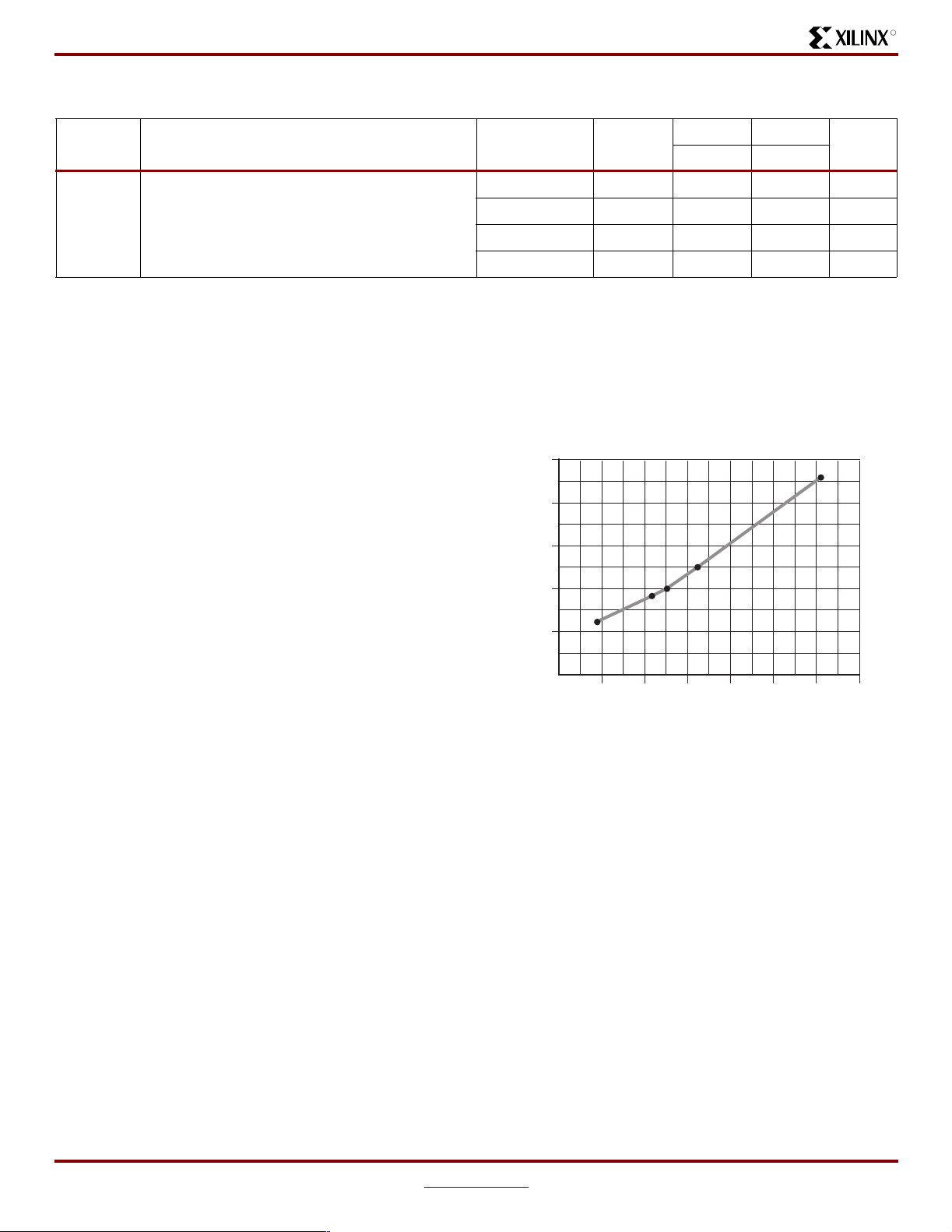
Figure 1 shows the rela tionship between I/O output del ay
and load capacitance. It allows a user to adjust the specified
output delay if the load capacitance is different than 50 pF.
For example, if the actual load capacitance is 120 pF, add
2.5 ns to the specified delay. If the load capacitance is
20 pF, subtract 0.8 ns from the specified output delay.
Figure 1 is usable over the specified operating conditions of
voltage and temperature and is i ndependent of the output
slew rate control.
3
2
1
0
Delta Delay (ns)
-1
-2
020406080
Capacitance (pF)
100 120 140
DS029_03_011300
Figure 1: Delay Factor at Various Capacitive Loads
12 www.xilinx.com DS029 (v1.3) June 25, 2000
1-800-255-7778 Product Specification
Page 13
R
QPRO XQ4000XL Series QML High-Reliability FPGAs
XQ4000XL Pin-to-Pin Input Parameter Guidelines
Testing of switching parameters is modeled after testing
methods specified by MIL-M-38510/605. All devices are
100% functionally tested. Pin-to-pin timing parameters are
derived from measuring external and inter nal test patterns
and are guaranteed over worst-case operating conditions
(supply voltage and junction temperature). Listed below are
representative values for typical pin locations and nor mal
worst-case guaranteed data, reflecting the actual routing
structure, use the values provided by the static timing analyzer (TRCE in the Xilinx Development System) and
back-annotated to the simulation netlist. These path delays,
provided as a guideline, have been extracted from the static
timing analyzer report. Values are expressed in nanoseconds unless otherwise noted.
clock loading. For more specific, more precise, and
Global Low Skew Clock, Input Setup and Hold Times
Symbol Description Device
No Delay
T
PSN/TPHN
Partial Delay
T
PSP/TPHP
Global early clock and IFF
Global early clock and FCL
Global early clock and IFF
Global early clock and FCL
(3)
(4)
(3)
(4)
(1,2)
-3 -1
(1)
XQ4013XL 1.2 / 3.2 - ns
XQ4036XL 1.2 / 5.5 - ns
XQ4062XL 1.2 / 7.0 - ns
XQ4085XL - 0.9 / 7.1 ns
XQ4013XL 6.1 / 0.0 - ns
XQ4036XL 6.4 / 1.0 - ns
XQ4062XL 6.7 / 1.2 - ns
UnitsMin Min
XQ4085XL - 9.8 / 1.2 ns
Full Delay
T
PSD/TPHD
Global early clock and IFF
(3)
XQ4013XL 6.4 / 0.0 - ns
XQ4036XL 6.6 / 0.0 - ns
XQ4062XL 6.8 / 0.0 - ns
XQ4085XL - 9.6 / 0.0 ns
Notes:
1. The XQ4013XL, XQ4036XL, and XQ4062 XL have significantly faster partial and full delay set up ti m es than other devic es.
2. Input setup t ime is measur ed wit h the fastest route and the light est load. Input hold t im e is measu red using t he furthest di stance and
a reference load o f one clock pin per IOB as well as driv ing all accessible CLB flip-flops. For d esigns with a sm aller number of clock
loads, the pad-to-IOB clock pin del ay as determined by the static timing analyzer (TRCE) can be used as a worst-case pin-to-pin
no-delay input hold specification.
3. IFF = Input Flip-Flop or Latch
4. FCL = Fast Capture Latch
DS029 (v1.3) June 25, 2000 www.xilinx.com 13
Product Specification 1-800-255-7778
Page 14
QPR O XQ4000X L Series QML High-Reliability FPGAs
R
Global Early Clock BUFEs 1, 2, 5, and 6 Setup and Hold for IFF and FCL
(1,2)
-3 -1
Symbol Description Device
Min Min
No Delay
T
PSEN/TPHEN
T
PFSEN/TPFHEN
Global early clock and IFF
Global early clock and FCL
(3)
(4)
XQ4013XL 1.2 / 4.7 XQ4036XL 1.2 / 6.7 XQ4062XL 1.2 / 8.4 XQ4085XL - 0.9 / 6.6
Partial Delay
T
PSEPN/TPHEP
T
PFSEP/TPFHEP
Global early clock and IFF
Global early clock and FCL
(3)
(4)
XQ4013XL 6.4 / 0.0 XQ4036XL 7.0 / 0.8 XQ4062XL 9.0 / 0.8 XQ4085XL - 11.0 / 0.0
Full Delay
T
PSEPD/TPHED
Global early clock and IFF
(3)
XQ4013XL 12.0 / 0.0 XQ4036XL 13.8 / 0.0 XQ4062XL 13.1 / 0.0 XQ4085XL - 13.6 / 0.0
Notes:
1. The XQ4013XL, XQ4036XL, and XQ4062 XL have significantly faster partial and full delay set up ti m es than other devic es.
2. Input setup t ime is measur ed wit h the fastest route and the light est load. Input hold t im e is measu red using t he furthest di stance and
a reference load o f one clock pin per IOB as well as driv ing all accessible CLB flip-flops. For d esigns with a sm aller number of clock
loads, the pad-to-IOB clock pin del ay as determined by the static timing analyzer (TRCE) can be used as a worst-case pin-to-pin
no-delay input hold specification.
3. IFF = Input Flip-Flop or Latch
4. FCL = Fast Capture Latch
14 www.xilinx.com DS029 (v1.3) June 25, 2000
1-800-255-7778 Product Specification
Page 15

R
QPRO XQ4000XL Series QML High-Reliability FPGAs
Global Early Clock BUFEs 3, 4, 7, and 8 Setup and Hold for IFF and FCL
(1,2)
-3 -1
Symbol Description Device
Min Min
No Delay
T
PSEN/TPHEN
T
PFSEN/TPFHEN
Global early clock and IFF
Global early clock and FCL
(3)
(4)
XQ4013XL 1.2 / 4.7 XQ4036XL 1.2 / 6.7 XQ4062XL 1.2 / 8.4 XQ4085XL - 0.9 / 6.6
Partial Delay
T
PSEPN/TPHEP
T
PFSEP/TPFHEP
Global early clock and IFF
Global early clock and FCL
(3)
(4)
XQ4013XL 5.4 / 0.0 XQ4036XL 6.4 / 0.8 XQ4062XL 8.4 / 1.5 XQ4085XL - 11.0 / 0.0
Full Delay
T
PSEPD/TPHED
Global early clock and IFF
(3)
XQ4013XL 10.0 / 0.0 XQ4036XL 12.2 / 0.0 XQ4062XL 13.1 / 0.0 XQ4085XL - 13.6 / 0.0
Notes:
1. The XQ4013XL, XQ4036XL, and XQ4062 XL have significantly faster partial and full delay set up ti m es than other devic es.
2. Input setup t ime is measur ed wit h the fastest route and the light est load. Input hold t im e is measu red using t he furthest di stance and
a reference load o f one clock pin per IOB as well as driv ing all accessible CLB flip-flops. For d esigns with a sm aller number of clock
loads, the pad-to-IOB clock pin del ay as determined by the static timing analyzer (TRCE) can be used as a worst-case pin-to-pin
no-delay input hold specification.
3. IFF = Input Flip-Flop or Latch
4. FCL = Fast Capture Latch
DS029 (v1.3) June 25, 2000 www.xilinx.com 15
Product Specification 1-800-255-7778
Page 16

QPR O XQ4000X L Series QML High-Reliability FPGAs
XQ4000XL IOB Input Switching Characteristic Guidelines
R
Testing of switching parameters is modeled after testing
methods specified by MIL-M-38510/605. All devices are
100% functionally tested. Internal timing parameters are
derived from measuri ng i nter n al t est patter ns. Listed below
are representative values. For mo re specific, more precise,
and worst-case guaranteed data, use t he values reported
by the static timing analyzer (TRCE in the Xilinx Development System) an d back-ann otated to th e simu lation n etlist.
These path delays, provided as a guideline, have been
extracted from the static timing analyzer report. All timing
parameters assume worst-case operating conditions (supply voltage and junction temperature)
Symbol Description Device
Clocks
T
T
OKIK
ECIK
Clock enable (EC) to clock (IK) All devices 0.1 - 0.1 - ns
Delay from FCL enable (OK) active edge to IFF
All device s 2.2 - 1.6 - ns
clock (IK) active edge
Setup Times
T
PICK
T
PICKF
Pad to clock (IK), no delay All devices 1. 7 - 1.3 - ns
Pad to clock (IK), via transparent fast capture latch,
All device s 2.3 - 1.8 - ns
no delay
T
POCK
Hold Times
Pad to fast capture latch enable (OK), no delay All devices 1.2 - 0.9 - ns
All Hold Times All devices 0 - 0 - ns
Global Set/Reset
T
T
MRW
RRI
Minimum GSR pulse width All devices - 19.8 - 15.0 ns
Delay from GSR input to any Q
(2)
XQ4013XL - 15.9 - - ns
XQ4036XL - 22.5 - - ns
XQ4062XL - 29.1 - - ns
.
-3 -1
UnitsMinMaxMinMax
Propagation Delays
T
T
T
PID
PLI
PFLI
Pad to I1, I2 All devices - 1.6 - 1.7 ns
Pad to I1, I2 via transparent input latch, no delay All devices - 3.1 - 2.4 ns
Pad to I1, I 2 via transparent FCL and input latch, no
delay
T
T
T
IKRI
IKLI
OKLI
Clock (IK) to I1, I2 (flip-flop) All devices - 1.7 - 1.3 ns
Clock (IK) to I1, I2 (latch enable, active Low) All devices - 1.8 - 1.4 ns
FCL enable (OK) active edge to I1, I2
(via transparent standard input latch)
Notes:
1. IFF = Input Flip-Flop or Latch, FCL = Fast Capture Latch
2. Indicates Minimum Am ount of Time to Assure Valid Data.
XQ4085XL - - - 26.0 ns
All devices - 3.7 - 2.8 ns
All devices - 3.6 - 2.7 ns
16 www.xilinx.com DS029 (v1.3) June 25, 2000
1-800-255-7778 Product Specification
Page 17

R
QPRO XQ4000XL Series QML High-Reliability FPGAs
XQ4000XL IOB Out put Sw itchin g Cha ract erist ic Gu ide lin es
Testing of switching parameters is modeled after testing
methods specified by MIL-M-38510/605. All devices are
100% functionally tested. Internal timing parameters are
derived from measuri ng i nter n al t est patter ns. Listed below
are representative values. For mo re specific, more precise,
and worst-case guaranteed data, use t he values reported
by the static ti ming analyzer (TR CE in the Xilinx Develop-
Symbol Description
Clocks
T
CH
T
CL
Clock High 3.0 - 2.5 - ns
Clock Low 3.0 - 2.5 - ns
Propagation Delays
T
OKPOF
T
OPF
T
TSHZ
T
TSONF
T
OFPF
T
OKFPF
Clock (OK) to pad - 5. 0 - 3.8 ns
Output (O) to pad - 4.1 - 3.1 ns
High-Z to pad High-Z (slew-rate independent) - 4.4 - 3.0 ns
High-Z to pad active and valid - 4.1 - 3.3 ns
Output (O) to pad via fast output MUX - 5.5 - 4.2 ns
Select (OK) to pad via f a st MUX - 5.1 - 3.9 ns
Setup and Hold Times
T
OOK
T
OKO
T
ECOK
T
OKEC
Output (O) to clock (OK) setup time 0.5 - 0.3 - ns
Output (O) to clock (OK) hold time 0 - 0 - ns
Clock Enable (EC) to clock (OK) setup time 0 - 0 - ns
Clock Enable (EC) to clock (OK) hold time 0.3 - 0.1 - ns
Global Set/Reset
T
T
MRW
RPO
Minimum GSR pulse width 19.8 - 15.0 - ns
Delay from GSR input to any pad
(2)
XQ4013XL - 20.5 - - ns
XQ4036XL - 27.1 - - ns
ment System) an d back-ann otated to th e simu lation n etlist.
These path delays, provided as a guideline, have been
extracted from the static timing analyzer report. All timing
parameters assume worst-case operating conditions (supply voltage and junction temperature). For Propagation
Delays, slew-rate = fast unless otherwise noted. Va lues are
expressed in nanoseconds unless otherwise noted.
-3 -1
UnitsMin Max Min Max
XQ4062XL - 33.7 - - ns
XQ4085XL - - 29.5 ns
Slew Rate Adjustment
T
SLOW
Notes:
1. Output timing is measured at ~50% V
2. Indicates Minimum Am ount of Time to Assure Valid Data.
DS029 (v1.3) June 25, 2000 www.xilinx.com 17
Product Specification 1-800-255-7778
For output SLOW option add - 3.0 - 2.0 ns
threshold, with 50 pF external capacitive loads.
CC
Page 18

QPR O XQ4000X L Series QML High-Reliability FPGAs
R
CB228 Pinouts
Table 2: CB228 Package Pinouts
Pin Name CB228
VTT
GND P1
BUFGP_TL_A16_GCK1_IO P2
A17_IO P3
IO P4
IO P5
TDI_IO P6
TCK_IO P7
IO P8
IO P9
IO P10
IO P11
IO P12
IO P13
GND P14
IO_FCLK1 P15
IO P16
TMS_IO P17
IO P18
IO P19
IO P20
IO P21
IO P22
IO P23
IO P24
IO P25
IO P26
GND P27
V
CC
IO P29
IO P30
IO P31
IO P32
IO P33
IO P34
IO P35
IO P36
V
CC
IO P38
P28
P37
Table 2: CB228 Package Pinouts (Continued)
Pin Name CB228
IO P39
IO P40
IO_FCLK2 P41
GND P42
IO P43
IO P44
IO P45
IO P46
IO P47
IO P48
IO P49
IO P50
IO P51
IO P52
IO P53
BUFGS_BL_GCK2_IO P54
M1 P55
GND P56
M0 P57
V
CC
M2 P59
BUFGP_BL_GCK3_IO P60
HDC_IO P61
IO P62
IO P63
IO P64
LDC_IO P65
IO P66
IO P67
IO P68
IO P69
IO P70
IO P71
GND P72
IO P73
IO P74
IO P75
IO P76
IO P77
IO P78
P58
18 www.xilinx.com DS029 (v1.3) June 25, 2000
1-800-255-7778 Product Specification
Page 19

R
QPRO XQ4000XL Series QML High-Reliability FPGAs
Table 2: CB228 Package Pinouts (Continued)
Pin Name CB228
IO P79
IO P80
IO P81
IO P82
IO P83
/ERR_INIT_IO P84
V
CC
P85
GND P86
IO P87
IO P88
IO P89
IO P90
IO P91
IO P92
IO P93
IO P94
V
CC
P95
IO P96
IO P97
IO P98
IO P99
GND P100
IO P101
IO P102
IO P103
IO P104
IO P105
IO P106
IO P107
IO P108
IO P109
IO P110
IO P111
BUFGS_BR_GCK4_IO P112
GND P113
DONE P114
V
CC
P115
/PROGRAM P116
D7_IO P117
BUFGP_BR_GCK5_IO P118
Table 2: CB228 Package Pinouts (Continued)
Pin Name CB228
IO P119
IO P120
IO P121
IO P122
D6_IO P123
IO P124
IO P125
IO P126
IO P127
IO P128
GND P129
IO P130
IO P131
IO_FCLK3 P132
IO P133
D5_IO P134
/CS0_IO P135
IO P136
IO P137
IO P138
IO P139
D4_IO P140
IO P141
V
CC
P142
GND P143
D3_IO P144
/RS_IO P145
IO P146
IO P147
IO P148
IO P149
D2_IO P150
IO P151
V
CC
P152
IO P153
IO_FCLK4 P154
IO P155
IO P156
GND P157
IO P158
DS029 (v1.3) June 25, 2000 www.xilinx.com 19
Product Specification 1-800-255-7778
Page 20

QPR O XQ4000X L Series QML High-Reliability FPGAs
R
Table 2: CB228 Package Pinouts (Continued)
Pin Name CB228
IO P159
IO P160
IO P161
IO P162
IO P163
D1_IO P164
BUSY_/RDY_RCLK_IO P165
IO P166
IO P167
D0_DIN_IO P168
BUFGS_TR_GCK6_DOU T_IO P169
CCLK P170
V
CC
P171
TDO P172
GND P173
A0_/WS_IO P174
BUFGP_TR_GCK7_A1_IO P175
IO P176
IO P177
CSI_A2_IO P178
A3_IO P179
IO P180
IO P181
IO P182
IO P183
IO P184
IO P185
GND P186
IO P187
IO P188
IO P189
IO P190
V
CC
P191
A4_IO P192
A5_IO P193
IO P194
IO P195
A21_IO P196
A20_IO P197
A6_IO P198
Table 2: CB228 Package Pinouts (Continued)
Pin Name CB228
A7_IO P199
GND P200
V
CC
P201
A8_IO P202
A9_IO P203
A19_IO P204
A18_IO P205
IO P206
IO P207
A10_IO P208
A11_IO P209
V
CC
P210
IO P211
IO P212
IO P213
IO P214
GND P215
IO P216
IO P217
IO P218
IO P219
A12_IO P220
A13_IO P221
IO P222
IO P223
IO P224
IO P225
A14_IO P226
BUFGS_TL_GCK8_A1 5_IO P227
V
CC
P228
20 www.xilinx.com DS029 (v1.3) June 25, 2000
1-800-255-7778 Product Specification
Page 21

R
Ordering Information
Example for QPRO™ military temperature par t:
XQ 4062XL -3 PG 475 M
QPRO XQ4000XL Series QML High-Reliability FPGAs
Mil-PRF-38535
(QML) Processed
Device Type
XQ4085XL
XQ4062XL
XQ4036XL
XQ4013XL
Speed Grade
-3
-1 (XQ4085XL only)
Example for SMD part
:
Generic Standard
Microcircuit Drawing (SMD)
Prefix
Device Type
XQ4013XL = 98513
XQ4036XL = 98510
XQ4062XL = 98511
XQ4085XL = 99575
Speed Grade
01 = -3 for XQ4103XL/4036XL/4062XL
01 = -1 for XQ4085XL
5962 98511 01 Q X C
Temp erature Range
M = Militar y C e ram ic (T
N = Military Plastic (T
= –55oC to +125 oC)
C
= –55°C to +125°C)
J
Number of Pins
Package T ype
CB = T op Braz ed Ceramic Quad Flat Pack
PG = Ceramic Pin Grid Ar ray
PQ/HQ = Plastic Quad Flat Back
BG = Plastic Ba ll Grid Array
Lead Fini sh
C = Gold
B = Solder
Package T ype
X = Pin Grid
Y = Ceramic Quad Flat Pack (Base Mark)
Z = Ceramic Quad Flat Pack (Lid Mark)
T = Plastic Quad Flat Pack
U = Plas t ic Ball Gr id
Q = QML Cert if ied
N = QML Plastic (N - Grade)
Revision History
The following table shows the revision history for this document
Date Version Description
05/01/98 1.0 Original document release.
01/01/99 1.1 Addition of new packages, clarification of parameters.
02/09/00 1.2 Addition of XQ4085XL-1 speed grade part.
06/25/00 1.3 Updated timing specifications to match with commercial data sheet. Updated format.
DS029 (v1.3) June 25, 2000 www.xilinx.com 21
Product Specification 1-800-255-7778
Page 22

QPR O XQ4000X L Series QML High-Reliability FPGAs
R
22 www.xilinx.com DS029 (v1.3) June 25, 2000
1-800-255-7778 Product Specification
 Loading...