

Page 1

查询XCR5128-10PQ100C供应商
This product has been disco ntinued. P lease see www.xilinx.com/partinfo/notify/p dn0007.htm for details.
APPLICATION NOTE
0
R
XCR5128: 128 Macrocell CPLD
DS041 (v1.4) January 19, 2001
0 14*
Features
• Industry's first TotalCMOS™ PLD - both CMOS design
and process technologies
• Fast Zero Power (FZP™) design technique provides
ultra-low power and very high speed
• IEEE 1149.1-compliant, JTAG Testing Capability
- Four pin JTAG interface (TCK, TMS, TDI, TDO)
- IEEE 1149.1 TAP Controller
- JTAG commands include: Bypass, Sample/Preload,
Extest, Usercode, Idcode, HighZ
• 5V, In- System Programmable (ISP) using the JTAG
interface
- On-chip supervoltage generation
- ISP commands include: Enable, Erase, Program,
Verify
- Supported by multiple ISP programming platforms
• High speed pin-to-pin delays of 7.5 ns
• Ultra-low static power of less than 100 µA
• 100% routable with 100% utilization while all pins and
all macrocells are fixed
• Deterministic timing model that is extremely simple to
use
• Four clocks available
• Programmable clock polarity at every macrocell
• Support for asynchronous clocking
• Innovative XPLA™ architecture combines high speed
with extreme flexibility
• 1000 erase/program cycles guaranteed
• 20 years data retention guaranteed
• Logic expandable to 37 product terms
•PCI compliant
2
• Advanced 0.5µ E
• Security bit prevents unauthorized access
• Design entry and verification using industry standard
and Xilinx CAE tools
• Reprogrammable using industry standard device
programmers
• Innovative Control Term structure provides either sum
terms or product terms in each logic block for:
- Programmable 3-state buffer
- Asynchronous macrocell register preset/reset
• Programmable global 3-state pin facilitates "bed of
nails" testing without using logic resources
• Available in PLCC, VQFP, and PQFP packages
• Available in both Commercial and Industrial grades
CMOS process
Product Specification
Description
The XCR5128 CPLD (Complex Programmable Logic
Device) is the third in a family of CoolRunner
Xilinx. These devices combine high speed and zero power
in a 128 macrocell CPLD. With the FZP design technique,
the XCR5128 offers true pin-to-pin speeds of 7.5 ns, while
simultaneously delivering power that is less than 100 µA at
standby without the need for ‘turbo bits' or other power
down schemes. By replacing conventional sense amplifier
methods for implementing product ter ms (a technique that
has been used in PLDs since the bipolar era) with a cascaded chain of pure CMOS gates, the dynamic power is
also substantially lower than any competing CPLD. These
devices are the first TotalCMOS PLDs, as they use both a
CMOS process technology and the patented full CMOS
FZP design technique. For 3V applications, Xilinx also
offers the high-speed XCR3128 CPLD that offers these f eatures in a full 3V implementation.
The Xilinx FZP CPLDs utilize the patented XPLA
(eXtended Programmable Logic Array) architecture. The
XPLA architecture combines the best features of both PLA
and PAL type structures to deliver high speed a nd flexible
logic allocation that results in superior ability to make
design changes with fixed pinouts. The XPLA structure in
each logic block provides a fast 7.5 ns PA L path with five
dedicated product terms per output. This PAL path is joined
by an additional PLA structure that de ploys a pool of 32
product terms to a fully programmable OR array that can
allocate the PLA product ter ms to any output in the logic
block. This combination allows logic to be allocated efficiently throughout the logic block and supports as many as
37 product terms on an output. The speed with which logic
is allocated from the PLA array to an output is only 2 ns,
regardless of the number of PLA product terms used, which
results in worst case t
other pin. In addition, logic that is common to multiple outputs can be placed on a single PLA product term and
shared across multiple outputs via the OR array, effectively
increasing design density.
The XCR5128 CPLDs are supported by industry standard
CAE tools (Cadence/OrCAD, Exemplar Logic, Mentor , Synopsys, Synario, Viewlogic, and Synplicity), using text
(ABEL, VHDL, Verilog) and/or schematic entry . Design v erification uses industry standard simulators for functional
and timing simulation. Development is supported on personal computer, Sparc, and HP platforms. Device fitting
's of only 9.5 ns from any pin to any
PD
®
CPLDs from
DS041 (v1.4) January 19, 2001 www.xilinx.com 1
1-800-255-7778
Page 2
R
This product has been discontinued. Pleas e see www.xilinx.com/partinfo/notify/pdn0007.htm for details.
XCR5128: 128 Macrocell CP LD
uses a Xilinx developed tool, XPLA Professional (available
on the Xilinx web site).
The XCR5128 CPLD is electrically reprogrammable using
industry standard device programmers from vendors such
as Data I/O, BP Microsystems, SMS, and others. The
XCR5128 also includes an industry-standard, IEEE
1149.1, JTAG interface through which in-system program-
ming (ISP) and reprogramming of the device is supported.
XPLA Architecture
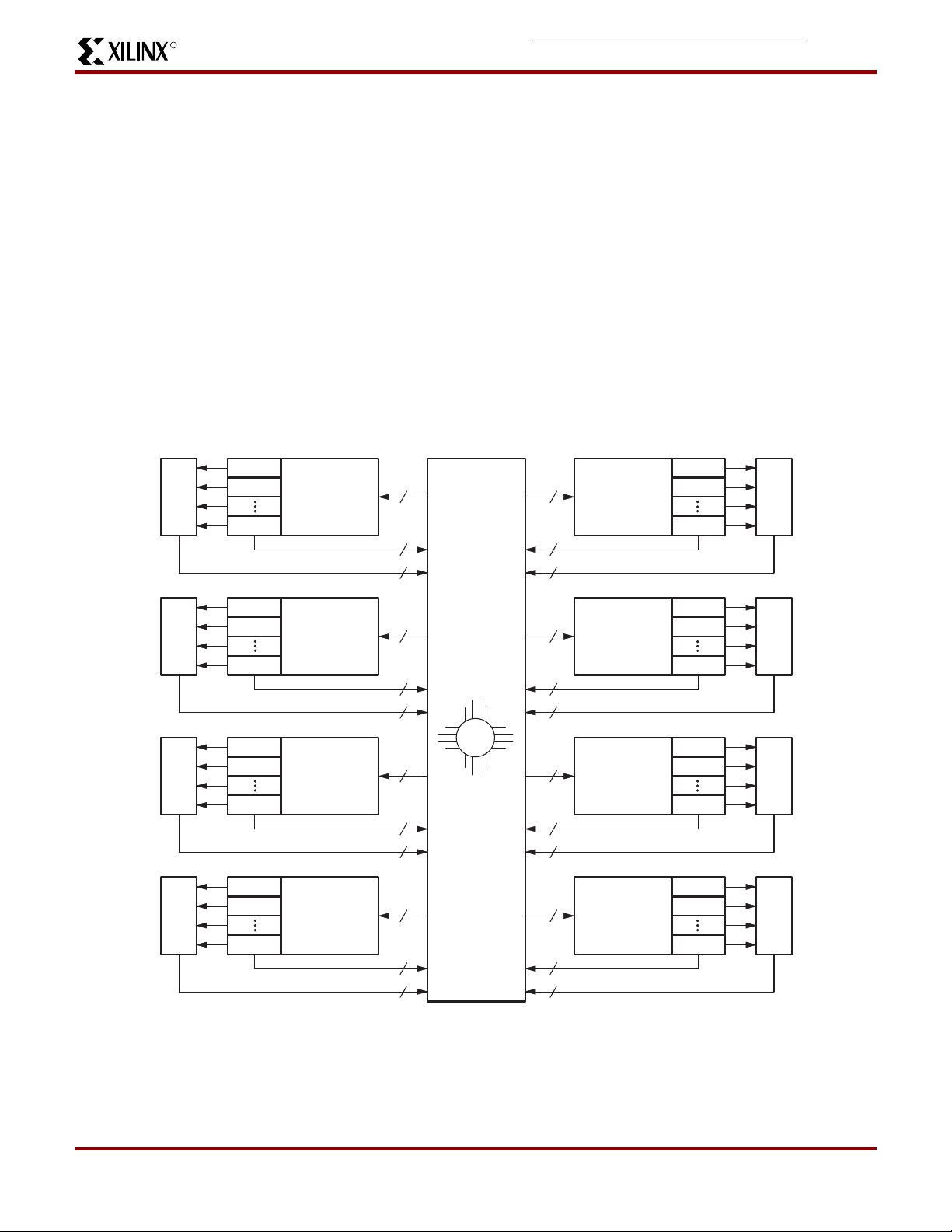
Figure 1 shows a high level block diagram of a 128 macro-
cell device implementing the XPLA architecture. The XPLA
MC1
I/O
MC2
MC16
LOGIC
BLOCK
36
16
16
architecture consists of logic bl ock s that ar e interconnected
by a Zero-power Interconnect Array (ZIA). The ZIA is a virtual crosspoint switch. Each logic block is essentially a
36V16 device with 36 inputs from the ZIA and 16 macrocells. Each logic bloc k als o provides 32 ZIA feedback paths
from the macrocells and I/O pins.
From this point of view, this architecture looks like many
other CPLD architectures. What makes the CoolRunner
family unique is what is inside each logic block and the
design technique used to implement these logic blocks.
The contents of the logic block will be described next.
MC1
36
16
16
LOGIC
BLOCK
MC2
MC16
I/O
I/O
I/O
I/O
MC1
MC2
MC16
MC1
MC2
MC16
MC1
MC2
MC16
LOGIC
BLOCK
LOGIC
BLOCK
LOGIC
BLOCK
MC1
36
16
16
ZIA
36
16
16
36
16
16
36
16
16
36
16
16
36
16
16
LOGIC
BLOCK
LOGIC
BLOCK
LOGIC
BLOCK
MC2
MC16
MC1
MC2
MC16
MC1
MC2
MC16
I/O
I/O
I/O
SP00464
Figure 1: Xilinx XPLA CPLD Architecture
DS041 (v1.4) January 19, 2001 www.xilinx.com 2
1-800-255-7778
Page 3

This product has been discon tinued. P lease see www.xilinx.com/partinfo/notify/pdn0007.htm for d etails.
XCR5128: 128 Macrocell CPLD
R
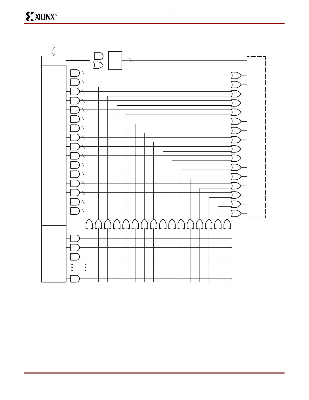
Logic Block Architecture
Figure 2 illustrates the logic block architecture. Each logic
block contains control terms, a PAL array, a PLA array, and
16 macrocells. the six control terms can individually be configured as either SUM or PRODUCT terms, and are used to
control the preset/reset and output enables of the 16 macrocells’ flip-flops. The PAL array consists of a programmable AND array with a fixed OR array, while the PLA array
consists of a programmable AND array with a programmable OR array. The PAL array provides a high speed path
through the array, while the PLA array provides increased
product term density.
Each macrocell has five dedicated product terms from the
PAL array. The pin-to-pin t
of the XCR5128 device
PD
through the PAL array is 7.5 ns. If a macrocell needs more
than five product terms, it simply gets the additional product
terms from the PLA array. The PLA array consists of 32
product terms, which are available for use by all 16 macrocells. The additional propagation delay incurred by a macrocell using one or all 32 PLA product terms is just 2 ns. So
the total pin-to-pin t
for the XCR5128 using six to 37
PD
product terms is 9.5 ns (7.5 ns for the PAL + 2 ns for the
PLA)
.
3 www.xilinx.com DS041 (v1.4) January 19, 2001
1-800-255-7778
Page 4
R
36 ZIA INPUTS
This product has been discontinued. Pleas e see www.xilinx.com/partinfo/notify/pdn0007.htm for details.
XCR5128: 128 Macrocell CP LD
CONTROL
PAL
ARRAY
6
5
TO 16 MACROCELLS
PLA
ARRAY
(32)
SP00435A
Figure 2: Xilinx XPLA Logic Block Architecture
DS041 (v1.4) January 19, 2001 www.xilinx.com 4
1-800-255-7778
Page 5
This product has been discon tinued. P lease see www.xilinx.com/partinfo/notify/pdn0007.htm for d etails.
XCR5128: 128 Macrocell CPLD
R
Macrocell Architecture
Figure 3 shows the architecture of the macrocell used in
the CoolRunner family. The macrocell consists of a flip-flop
that can be configured as either a D- or T- type. A D-type
flip-flop is generally more useful for implementing state
machines and data buffering. A T-typ e flip-flop is generally
more useful in implementing counters. All CoolRunner family members provide both synchronous and asynchronous
clocking and provide the ability to clock off either the falling
or rising edges of these clocks. These devices are
designed such that the skew between the rising and falling
edges of a clock are minimized for clocking integrity. There
are four clocks available on the XCR5128 device. Clock 0
(CLK0) is designated as the "synchronous" clock and must
be driven by an external source. Clock 1 (CLK1), Clock 2
(CLK2), and Clock 3 (CLK3) can either be used as a synchronous clock (driven by an external source) or as an
asynchronous clock (driven by a macrocell equation). The
timing for asynchronous clocks is different in that the t
time is extended by the amount of time that it takes for the
signal to propagate through the array and reach the clock
network, and the t
time is reduced.
SU
Two of the control terms (CT0 and CT1) are used to control
the Preset/Reset of the macrocell’s flip-flop. The Preset/Reset feature for each macrocell can also be disabled.
Note that the Power-on Reset leaves all macrocells in the
"zero" state when power is properly applied. The other four
CO
control terms (CT2-CT5) can be used to control the Output
Enable of the macrocell’s output buffers. The reason there
are as many control terms dedicated for the Output Enable
of the macrocell is to insure that all CoolRunner devices are
PCI compliant. The macrocell’s output buffers can also be
always enabled or disabled. All CoolRunner devices also
provide a Global 3-State (GTS) pin, which, when enabled
and pulled Low, will 3-state all the outputs of the device.
This pin is provided to support "In-Circuit Testing" or
"Bed-of-Nails Testing".
There are two feedback paths to the ZIA: one from the macrocell, and one from the I/O pin. The ZIA feedback path
before the output buffer is the macrocell feedback path,
while the ZIA feedback path after the output buffer is the I/O
pin ZIA path. When the macrocell is used as an output, the
output buffer is enabled, and the macrocell feedback path
can be used to feedback the logic implemented in the macrocell. When the I/O pin is used as an input, the output
buffer will be 3-stated and the input signal will be fed into
the ZIA via the I/O feedback path, and the logic implemented in the buried macrocell can be fed back to the ZIA
via the macrocell feedback path. It should be noted that
unused inputs or I/Os should be properly terminated (see
the section on T erminations in this data sheet and the application note: Terminating Unused I/O Pins in xilinx XPLA1
and XPLA2 CPLDs).
PAL
PLA
CLK0
CLK0
CLK1
CLK1
CLK2
CLK2
CLK3
CLK3
Figure 3: XCR5128 Macrocell Architecture
D/T Q
INIT
(P or R)
TO ZIA
CT0
CT1
GND
GTS
CT2
CT3
CT4
CT5
V
GND
GND
CC
SP00457
5 www.xilinx.com DS041 (v1.4) January 19, 2001
1-800-255-7778
Page 6
R
This product has been discontinued. Pleas e see www.xilinx.com/partinfo/notify/pdn0007.htm for details.
XCR5128: 128 Macrocell CP LD
Simple Timing Model
Figure 4 shows the CoolRunner Timing Model. The C ool-
Runner timing model looks very much like a 22V10 timing
model in that there are three main timing parameters,
including t
tures, the user may be able to fit the design into the CPLD,
but is not sure whether system timing requirements can be
met until after the design has been fit into the device . This is
because the timing models of competing architectures are
very complex and include such things as timing dependencies on the number of parallel expanders borrowed, sharable expanders, varying number of X and Y routing
channels used, etc. In the XPLA architecture, the user
knows up front whether the design will meet system timing
requirements. This is due to the simplicity of the timing
model.
, tSU, and tCO. In other competing architec-
PD
t
PD_PAL
t
PD_PLA
REGISTERED
t
= PAL ONLY
SU_PAL
= PAL + PLA
t
SU_PLA
= COMBINATORIAL PAL ONLY
= COMBINATORIAL PAL + PLA
TotalCMOS De sign Technique for Fast Zero
Power
Xilinx is the first to offer a TotalCMOS CP LD, both in process technology and design technique. Xilinx employs a
cascade of CMOS gates to implement its Sum of Products
instead of the traditional sense amp approach. This CMOS
gate implementation allows Xilinx to offer CPLDs which are
both high performance and low power, breaking the paradigm that to have low power, you must have low performance. Refer to Figure 5 and Table 1 showing the I
Frequency of Xilinx’ XCR5128 TotalCMOS CPLD (data
taken w/eight up/down, loadable 16 bit counters at 5V,
25°C.
OUTPUT PININPUT PIN
REGISTERED
t
DQ
CO
OUTPUT PININPUT PIN
CC
vs.
GLOBAL CLOCK PIN
Figure 4: CoolRunner Timing Model
SP00441
DS041 (v1.4) January 19, 2001 www.xilinx.com 6
1-800-255-7778
Page 7

This product has been discon tinued. P lease see www.xilinx.com/partinfo/notify/pdn0007.htm for d etails.
XCR5128: 128 Macrocell CPLD
120
100
80
I
CC
(mA)
60
40
20
0
0 20406080100
FREQUENCY (MHz)
Figure 5: ICC vs. Frequency at VCC = 5V, 25°C
120
SP00465
R
Table 1: I
vs. Frequency (VCC = 5V, 25°C)
CC
Frequency (MHz) 0 1 20 40 60 80 100 120
Typical I
JTAG Te st i n g Capability
JTAG is the commonly-used acronym for the Boundary
Scan Test (BST) feature defined for integrated circuits by
IEEE Standard 1149.1. This standard defines input/output
pins, logic control functions , and commands which facilitate
both board and device level testing without the use of specialized test equipment. BST provides the ability to test the
external connections of a device, test the internal logic of
the device, and capture data from the device during normal
operation. BST provides a number of benefits in each of the
following areas:
• Testability
- Allows testing of an unlimited number of
interconnects on the printed circuit board
- Testability is designed in at the component level
- Enables desired signal levels to be set at specific
pins (Preload)
- Data from pin or core logic signals can be examined
during normal operation
• Reliability
- Eliminates physical contacts common to existing test
fixtures (e.g., "bed-of-nails")
- Degradation of test equipment is no longer a
concern
- Facilitates the handling of smaller, surface-mount
components
- Allows for testing when components exist on both
sides of the printed circuit board
(mA) 0.5 1 20 40 60 80 99 118
CC
• Cost
- Reduces/eliminates the need for expensive test
equipment
- Reduces test preparation time
- Reduces spare board inventories
The Xilinx XCR5128's JTAG interface includes a TAP Port
and a T AP Controller , both of which are defined by the IEEE
1149.1 JTAG Specification. As implemented in the Xilinx
XCR5128, the TAP Port includes four of the five pins (refer
to Table 2) described in the JTA G specification: TCK, TMS,
TDI, and TDO. The fifth signal defined by the JTAG specification is TRST* (Test Reset). TRST* is considered an
optional signal, since it is not actually required to perform
BST or ISP. The Xilinx XCR5128 saves an I/O pin for general purpose use by not implementing the optional TRST*
signal in the JTAG interface. Instead, the Xilinx XCR5128
supports the test reset functionality through the use of its
power up reset circuit, which is included in all Xilinx CPLDs.
The pins associated with the power up reset circuit should
connect to an external pull-up resistor to keep the JTAG
signals from floating when they are not being used.
In the Xilinx XCR5128, the four mandatory JT A G pins each
require a unique, dedicated pin on the device. However, if
JTAG and ISP are not desired in the end-application, these
pins may instead be used as additional general I/O pins.
The decision as to whether these pins are used for
JTAG/ISP or as general I/O is made when the JEDEC file is
generated. If the use of JTAG/ISP is selected, the dedi-
7 www.xilinx.com DS041 (v1.4) January 19, 2001
1-800-255-7778
Page 8
R
This product has been discontinued. Pleas e see www.xilinx.com/partinfo/notify/pdn0007.htm for details.
XCR5128: 128 Macrocell CP LD
cated pins are not available for general purpose use. However, unlike competing CPLD’s, the Xilinx XCR5128 does
allow the macrocell logic associated with these dedicated
pins to be used as buried logic even when JTAG/ISP is
selected. Table 3 defines the dedicated pins used by the
four mandatory JTAG signals for each of the XCR5128
package types.
JTAG specifications define two sets of commands to support boundary-scan testing: high-level commands and
low-level commands. High-level commands are executed
automated test equipment, a PC, or an engineering workstation (EWS). Each high-level command comprises a
sequence of low level commands. These low-level commands are executed within the component under test, and
therefore must be implemented as part of the TAP Controller design. The set of low-level boundar y-scan commands
implemented in the Xilinx XCR5128 is defined in Table 4 .
By supporting this set of low-level commands, the
XCR5128 allows execution of all high-level boundary-scan
commands.
via board test software on an a user test station such as
Table 2: JTAG Pin Description
Pin Name Description
TCK Test Clock Output Clock pin to shift the ser ial data and instructions in and out of the TDI and TDO pi ns,
respectively. TCK is also used to clock the TAP Controller state machine.
TMS Test M ode Select Serial input pin selects the JTAG instruction mode. TMS should be driven high
during user mode operation.
TDI Test Data Input Serial input pin for instructions and test data. Data is shifted in on the rising edge of
TCK.
TDO Test Data Output Serial output pin for instructions and test data. Data is shifted out on the falling edge
of TCK. The signal is tri-stated if data is not being shifted out of the device.
Table 3: XCR5128 J TAG Pinout by Package Type
Device
PZ5128
TCK TMS TDI TDO
(Pin Number / Macrocell #)
84-pin PLCC 62 / 96 (F15) 23 / 48 (C15) 14 / 32 (B15) 71 / 112 (G15)
100-pin PQFP 64 / 96 (F15) 17 / 48 (C15) 6 / 32 (B15) 75 / 112 (G15)
100-pin VQFP 62 / 96 (F15) 15 / 48 (C15) 4 / 32 (B15) 73 / 112 (G15)
128-pin TQFP 82 / 96 (F15) 21 / 48 (C15) 8 / 32 (B15) 95 / 112 (G15)
160-pin PQFP 99 / 96 (F15) 22 / 48 (C15) 9 / 32 (B15) 112/ 112 (G15)
Table 4: XCR5128 Low-Level JTAG Boundary-Scan Commands
Instruction
(Instruction Code)
Description
Register Used
Sample/Preload
(0010)
Boundary-Scan Register
The mandatory SAMPLE/PRELOAD instruction allows a snapsho t of the normal operation
of the component to be taken and examined. It also allows data values to be loaded onto the
latched parallel outputs of the Boundary-Scan Shift-Register prior to selection of the other
boundary-scan test instructions.
Extest
(0000)
Boundary-Scan Register
The mandatory EXTEST instruction allows testing of off-chip circuitry and board level
interconnections. Data would typically be loaded onto the latched parallel outputs of
Boundary-Scan Shift-Register using the Sample/Preload instruction prior to selection of the
EXTEST instruction.
Bypass
(1111)
Bypass Register
Places the 1 bit bypass register between the TDI and TDO pins, which allows the BST data
to pass synchronously through the selected device to adjacent devices during normal device
operation. The Bypass instruction can be entered by holding TDI at a constant high value
and completing an Instruction-Scan cycle.
DS041 (v1.4) January 19, 2001 www.xilinx.com 8
1-800-255-7778
Page 9

This product has been discon tinued. P lease see www.xilinx.com/partinfo/notify/pdn0007.htm for d etails.
XCR5128: 128 Macrocell CPLD
Table 4: XCR5128 Low-Level JTAG Boundary-Scan Commands
R
Idcode
(0001)
Boundary-Scan Register
Selects the IDCODE register and places it between TDI and TDO, allowing the IDCODE to
be serially shifted out of TDO. The IDCODE instruction permits blind interrogation of the
components assembled onto a printed circuit board. Thus, in circumstances where the
component population may vary, it is possible to determine what components exist in a
product.
HighZ
(0101)
Bypass Register
The HIGHZ instruction places the component in a state in which all
are placed in an inactive drive state (e.g., high impedance). In this state, an in-circuit test
system may drive signals onto the connections normally driven by a component output
without incurring the risk of damage to the component. The HighZ instruction also forces the
Bypass Register between TDI and TDO.
5V, In-System Programming (ISP)
ISP is the ability to reconfigure the logic and functionality of
a device, printed circuit board, or complete electronic system before, during, and after its manufacture and shipment
to the end customer. ISP provides substantial benefits in
each of the following areas:
• Design
- Faster time-to-market
- Debug partitioning and simplified prototyping
- Printed circuit board reconfiguration during debug
- Better device and board level testing
• Manufacturing
- Multi-Functional hardware
- Reconfigurability for Test
- Eliminates handling of "fine lead-pitch" components
for programming
- Reduced Inventory and manufacturing costs
- Improved quality and reliability
• Field Support
- Easy remote upgrades and repair
- Support for field configuration, re-configuration, and
customization
The Xilinx XCR5128 allows for 5V, in-system programming/reprogramming of its EEPROM cells via its JTAG
interface. An on-chip charge pump eliminates the need for
externally-provided supervoltages, so that the XCR5128
may be easily programmed on the circuit board using only
the 5V supply required by the device for normal operation.
A set of low-level ISP basic commands implemented in the
XCR5128 enable this feature. The ISP commands implemented in the Xilinx XCR5128 are specified in Table 6.
Please note that an ENABLE command must precede all
ISP commands unless an ENABLE command has already
been given for a preceding ISP command and the device
of its system logic outputs
has not gone through a Test-Logic/Rest TAP Controller
State.
Terminations
The CoolRunner XCR5128 CPLDs are TotalCMOS
devices. As with other CMOS devices, it is important to
consider how to properly terminate unused inputs and I/O
pins when fabricating a PC board. Allowing unused inputs
and I/O pins to float can cause the voltage to be in the l inear
region of the CMOS input structures, which can increase
the power consumption of the device. The XCR5128
CPLDs have programmable on-chip pull-down resistors on
each I/O pin. These pull-downs are automatically activated
by the fitter software for all unused I/O pins. Note that an I/O
macrocell used as buried logic that does not have the I/O
pin used for input is considered to be unused, and the
pull-down resistors will be turned on. We recommend that
any unused I/O pins on the XCR5128 device be left unconnected.
There are no on-chip pull-down structures associated with
the dedicated input pins. Xilinx recommends that any
unused dedicated inputs be terminated with external 10kΩ
pull-up resistors. These pins can be directly connected to
or GND, but using the external pull-up resistors main-
V
CC
tains maximum design flexibility should one of the unused
dedicated inputs be needed due to future design changes.
When using the JTAG/ISP functions, it is also recommended that 10kΩ pull-up resistors be used on each of the
pins associated with the four mandatory JTAG signals. Letting these signals float can cause the voltage on TMS to
come close to ground, which could cause the device to
enter JTAG/ISP mode at unspecified times. See the application notes JTAG and ISP Overview for Xilinx XPLA1 and
XPLA2 CPLDs and Terminating Unused I/O Pi ns in Xilinx
XPLA1 and XPLA2 CoolRunner CPLDs for more informa-
tion.
9 www.xilinx.com DS041 (v1.4) January 19, 2001
1-800-255-7778
Page 10
R
This product has been discontinued. Pleas e see www.xilinx.com/partinfo/notify/pdn0007.htm for details.
XCR5128: 128 Macrocell CP LD
JTAG and ISP Interfacing
A number of industry-established methods exist for
JTAG/ISP interfacing with CPLD’s and other integrated circuits. The Xilinx XCR5128 supports the following methods:
• PC parallel port
• Workstation or PC serial port
• Embedded processor
• Automated test equipment
Table 5: Low Level ISP Commands
Instruction
(Register Used)
Enable
(ISP Shift Register)
Erase
(ISP Shift Register)
Program
(ISP Shift Register)
Verify
(ISP Shift Register)
Instruction
Code
1001 Enables the Erase, Program, and Verify commands. Using the ENABLE instruction
before the Erase, Program, and Verify instructions allows the user to specify the
outputs the device using the JTAG Boundary-Scan SAMPLE/PRELOAD
command.
1010 Erases the entire EEPROM array. The outputs during this operation can be defined
by user by using the JTAG SAMPLE/PRELOAD comman d.
1011 Programs the data in the ISP Shift Register into the addressed EEPROM row. The
outputs during this operation can be defined by user by using the JTAG
SAMPLE/PRELOAD command.
1100 Transfers the data from the addressed row to the ISP Shift Register. The data can
then be shifted out and compared with the JEDEC file. The outputs during this
operation can be defined by user by using the JTAG SAMPLE/PRELOAD
command.
• Third party programmers
• High-End JTAG and ISP tools
A Boundary-Scan Description Language (BSDL) description of the XCR5128 is also available from Xilinx for use in
test program development. For more details on JTAG and
ISP for the XCR5128, refer to the related application note:
JTAG and ISP in Xilinx CPLDs.
Description
DS041 (v1.4) January 19, 2001 www.xilinx.com 10
1-800-255-7778
Page 11

This product has been discon tinued. P lease see www.xilinx.com/partinfo/notify/pdn0007.htm for d etails.
XCR5128: 128 Macrocell CPLD
Programming Specifications
Symbol Parameter Min. Max. Unit
DC Parameters
V
CCP
I
CCP
V
IH
V
IL
V
SOL
V
SOH
TDO_I
TDO_I
AC Parameters
f
MAX
PWE Pulse width erase 100 ms
PWP Pulse width program 10 ms
PWV Pulse width verify 10 µs
INIT Initialization time 100 µs
TMS_SU TMS setup time before TCK ↑ 10 ns
TDI_SU TDI setup time before TCK ↑ 10 ns
TMS_H TMS hold time after TCK ↑ 20 ns
TDI_H TDI hold time after TCK ↑ 20 ns
TDO_CO TDO valid after TCK ↓ 30 ns
VCC supply program/verify 4.5 5.5 V
ICC limit program/verify 200 mA
Input voltage (High) 2.0 V
Input voltage (Low) 0.8 V
Output voltage (Low) 0.5 V
Output voltage (High) 2.4 V
Output current (Low) 12 mA
OL
Output current (High) -12 mA
OH
CLK maximum frequency 10 MHz
R
Absolute Maximum Ratings
1
Symbol Parameter Min. Max. Unit
V
V
I
Notes:
Supply voltage
CC
V
OUT
I
OUT
T
T
Input voltage -1.2 V
I
Output voltage -0.5 V
Input current -30 30 mA
IN
Output current -100 100 mA
Maximum junction temperature -40 150 5C
J
Storage temperature -65 150 5C
str
1. Stresses above those listed may cause malf unction or permanent dam age to the device. This is a stress rating only.
Functional operation at these or any other condition above those indicated in the operational and programming specification
is not implied.
2. The chip supply voltage must ri se m onotonically.
2
-0.5 7.0 V
+0.5 V
CC
+0.5 V
CC
Operating Range
Product Grade Temperature Voltage
Commercial 0 to +70°C5.0V +5%
Industrial -40 to +85°C5.0V +10%
11 www.xilinx.com DS041 (v1.4) January 19, 2001
1-800-255-7778
Page 12
R
This product has been discontinued. Pleas e see www.xilinx.com/partinfo/notify/pdn0007.htm for details.
XCR5128: 128 Macrocell CP LD
DC Electrical Characteristics For Commercial Grade Devices
Commercial: 0°C ≤ T
≤ +70°C; 4.75V ≤ VCC ≤ 5.25V
AMB
Symbol Parameter Test Conditions Min. Max. Unit
V
V
V
V
V
I
I
I
OZ
I
CCQ
I
CCD
I
OS
IL
IH
I
OL
OH
Input voltage low VCC = 4.75V 0.8 V
Input voltage high VCC = 5.25V 2.0 V
Input clamp voltage V
= 4.75V, IIN = -18mA -1.2 V
CC
Output voltage low VCC = 4.75V, IOL = 12mA 0.5 V
Output voltage high VCC = 4.75V, IOH = -12mA 2.4 V
Input leakage current VIN = 0 to V
3-stated output leakage current VIN = 0 to V
Standby current VCC = 5.25V, T
2
Dynamic current VCC = 5.25V, T
Short circuit output current
3
CC
CC
= 0°C 100 µA
AMB
= 0°C at 1 MHz 5 mA
AMB
= 5.25V, T
V
CC
= 0°C at 50 MHz 75 mA
AMB
One pin at a time for no longer than 1
-10 10 µA
-10 10 µA
-50 -200 mA
second
C
IN
C
CLK
C
I/O
Notes:
Input pin capacitance
Clock input capacitance
I/O pin capacitance
1. See Table 1 on page 7 for typical values.
2. his parameter measured with a 16-bit, loadable up/down counter loaded into every logic block, with all outputs disabled and
unloaded. Inpu ts are tied to V
3. Typical valu e s , not tested.
3
3
3
or ground. This parameter gu aran te ed by desi gn and characterization, not testing.
CC
T
= 25°C, f = 1 MHz 8 pF
AMB
T
= 25°C, f = 1 MHz 5 12 pF
AMB
T
= 25°C, f = 1 MHz 10 pF
AMB
DS041 (v1.4) January 19, 2001 www.xilinx.com 12
1-800-255-7778
Page 13
This product has been discon tinued. P lease see www.xilinx.com/partinfo/notify/pdn0007.htm for d etails.
XCR5128: 128 Macrocell CPLD
AC Electrical Characteristics1 For Commercial Grade Devices
R
Commercial: 0°C ≤ T
≤ +70°C; 4.75V ≤ VCC ≤ 5.25V
AMB
Symbol Parameter
t
PD_PAL
Propagation delay time, input (or feedback node) to output
through PAL
t
PD_PLA
Propagation delay time, input (or feedback node) to output
through
PAL + PL A
t
CO
t
SU_PAL
t
SU_PLA
t
H
t
CH
t
CL
t
R
t
F
f
MAX1
f
MAX2
f
MAX3
t
BUF
t
PDF_PA L
Clock to out (global synchronous clock from pin)
Setup time (from input or feedback node) through PAL
Setup time (from input or feedback node) through PAL + PLA
Hold time
Clock High time
Clock Low time
Input Rise time
Input Fall time
Maximum FF toggle rate2 1/(tCH + tCL)
Maximum internal frequency2 1/(t
Maximum external frequency2 1/(t
Output buffer delay time
Input (or feedback node) to inter nal feedback node del ay time
through PAL
t
PDF_PL A
Input (or feedback node) to inter nal feedback node del ay time
through PAL+ PLA
t
CF
t
INIT
t
ER
t
EA
t
RP
t
RR
Notes:
Clock to internal feedback node delay time
Delay from valid VCC to valid reset
Input to output disable
Input to output valid
Input to register preset
Input to register reset
1. Specifications me asured with one output switching. S ee Figure 6 and Table 6 for derating.
2. This parameter guarant eed by desi gn and characteriza tion , not by test.
3. Output c
= 5 pf.
l
2, 3
2
2
2
SUPAL
SUPAL
+ tCF)
+ tCO)
71012
Min/ Max. Min. Max. Min. Max.
Unit
2 7.5 2 10 2 12 ns
3 9.5 3 12 3 14.5 ns
262728ns
4.5 7 8 ns
6.5 9 10.5 ns
000ns
344ns
344ns
20 20 20 ns
20 20 20 ns
167 125 125 MHz
111 80 69 MHz
95 71 63 MHz
1.5 1.5 1.5 ns
2 6 2 8.5 2 10.5 ns
3 8 3 10.5 3 13 ns
4.5 5.5 6.5 ns
50 50 50
µs
91215ns
91215ns
11 12.5 15 ns
11 12.5 15 ns
13 www.xilinx.com DS041 (v1.4) January 19, 2001
1-800-255-7778
Page 14

R
This product has been discontinued. Pleas e see www.xilinx.com/partinfo/notify/pdn0007.htm for details.
XCR5128: 128 Macrocell CP LD
DC Electrical Characteristics For Industrial Grade Devices
Industrial: -40°C ≤ T
≤ +85°C; 4.5V ≤ VCC ≤ 5.5V
AMB
Symbol Parameter Test Conditions Min. Max. Unit
V
V
V
V
V
I
I
I
OZ
I
CCQ
I
CCD
I
OS
IL
IH
I
OL
OH
Input voltage low VCC = 4.5V 0.8 V
Input voltage high VCC = 5.5V 2.0 V
Input clamp voltage VCC = 4.5V, IIN = -18 mA -1.2 V
Output voltage low VCC = 4.5V, IOL = 12 mA 0.5 V
Output voltage high VCC = 4.5V, IOH = -12 mA 2.4 V
Input leakage current VIN = 0 to V
3-stated output leakage current VIN = 0 to V
1
Standby current VCC = 5.5V, T
1, 2
Dynamic current VCC = 5.5V, T
Short circuit output current
3
CC
CC
= -40°C 125 µA
AMB
= -40°C at 1 MHz 6 mA
AMB
V
CC
= 5.5V, T
= -40°C at 50 MHz 90 mA
AMB
One pin at a time for no longer than 1
-10 10 µA
-10 10 µA
-50 -230 mA
second
C
IN
C
CLK
C
I/O
Notes:
Input pin capacitance
Clock input capacitance
I/O pin capacitance
1. See Table 1 on page 7 for typical values.
2. This parameter measured with a 16-bit, loadable up/down counter loaded into every logic block, with all outputs disabled
and unloaded. Input s are tied to V
3. Typical valu e s , not tested.
3
3
3
T
= 25°C, f = 1 MHz 8 pF
AMB
T
= 25°C, f = 1 MHz 5 12 pF
AMB
T
= 25°C, f = 1 MHz 10 pF
AMB
or ground. This parameter guar ant eed by design and characteriz ation , not te st in g.
CC
DS041 (v1.4) January 19, 2001 www.xilinx.com 14
1-800-255-7778
Page 15

This product has been discon tinued. P lease see www.xilinx.com/partinfo/notify/pdn0007.htm for d etails.
XCR5128: 128 Macrocell CPLD
AC Electrical Characteristics For Industrial Grade Devices
R
Industrial: -40°C ≤ T
≤ +85°C; 4.5V ≤ VCC ≤ 5.5V
AMB
Symbol Parameter
t
PD_PAL
t
PD_PLA
Propagation delay time, input (or feedback node) to output through PAL 2 10 2 15 ns
Propagation delay time, input (or feedback node) to output through PAL
& PLA
t
CO
t
SU_PAL
t
SU_PLA
t
H
t
CH
t
CL
t
R
t
F
f
MAX1
f
MAX2
f
MAX3
t
BUF
t
PDF_PAL
Clock to out (global synchronous clock from pin) 2728ns
Setup time (from input or feedback node) through PAL 8 8 ns
Setup time (from input or feedback node) through PAL + PLA 10 10.5 ns
Hold time 00ns
Clock High time 5 5 ns
Clock Low time 5 5 ns
Input Rise time 20 20 ns
Input Fall time 20 20 ns
Maximum FF toggle rate2 1/(tCH + tCL) 100 100 MHz
Maximum internal frequency2 1/(t
Maximum external frequency2 1/(t
SUPAL
SUPAL
Output buffer delay time 1.5 1.5 ns
Input (or feedback node) to internal feedback node delay time
through PAL
t
PDF_PLA
Input (or feedback node) to internal feedback node delay time through
PAL+ PLA
t
CF
t
INIT
t
ER
t
EA
t
RP
t
RR
Notes:
Clock to internal feedback node delay time 6 6.5 ns
Delay from valid VCC to valid reset 50 50 µs
Input to output disable
Input to output valid
Input to register preset
Input to register reset
1. Specifications me asured with one output switching. S ee Figure 6 and Table 6 for derating.
2. This parameter guarant eed by desi gn and characteriza tion , not by test.
3. Output C
= 5 pF.
L
2, 3
2
2
2
10 15
Min. Max. Min. Max.
Unit
312317.5ns
+ tCF)7169MHz
+ tCO)6663MHz
2 8.5 2 13.5 ns
3 10.5 3 16 ns
15 1 5 ns
15 1 5 ns
15 1 7 ns
15 1 7 ns
15 www.xilinx.com DS041 (v1.4) January 19, 2001
1-800-255-7778
Page 16
R
NUMBER OF OUTPUTS SWITCHING
1 2 4 8 12 16
6.0
t
PD_PAL
(ns)
6.4
6.8
7.2
VDD = 5V
, 25
°C
SP00472
7.6
8.0
8.4
This product has been discontinued. Pleas e see www.xilinx.com/partinfo/notify/pdn0007.htm for details.
Switching Characteristics
V
CC
XCR5128: 128 Macrocell CP LD
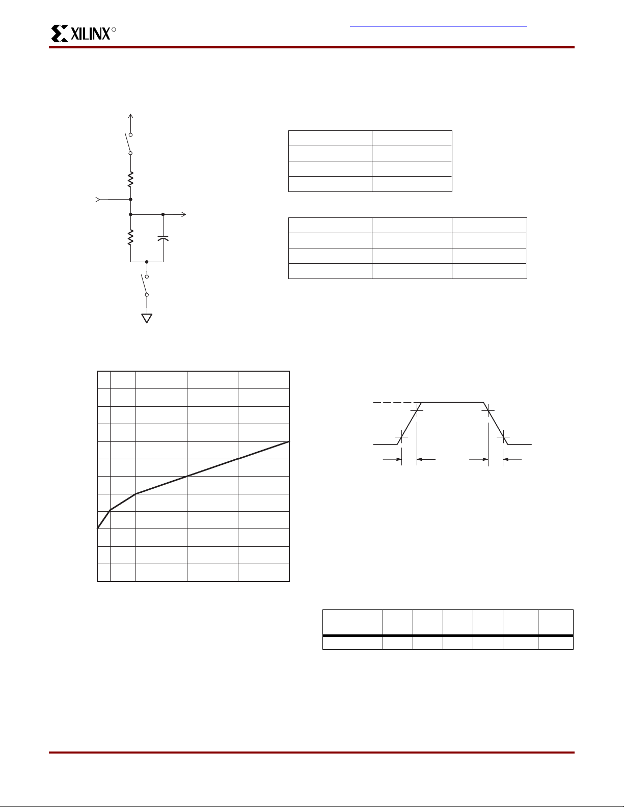
S1
COMPONENT VALUES
R1 470Ω
R2 250Ω
R1
V
IN
V
OUT
C1 35 pF
MEASUREMENT S1 S2
R2
S2
C1
t
PZH
t
PZL
t
P
Open Closed
Closed Open
Closed Closed
Note: For tPHZ and tPLZ C = 5 pF.
SP00458A
Vo ltage Waveform
+3.0V
90%
Figure 6: t
0V
t
RtF
MEASUREMENTS:
All circuit delays are measured at the +1.5V level of
inputs and outputs, unless otherwise specified.
Input Pulses
Table 6: t
vs. Number of Outputs Switching
PD_PAL
10%
1.5ns1.5ns
SP00368
(VCC = 5V)
vs. Outputs Switching
PD_PAL
Number Of
Outputs
1 2 4 8 12 16
Typical (ns) 6.6 6.8 7.0 7.2 7.4 7.6
DS041 (v1.4) January 19, 2001 www.xilinx.com 16
1-800-255-7778
Page 17
This product has been discon tinued. P lease see www.xilinx.com/partinfo/notify/pdn0007.htm for d etails.
XCR5128: 128 Macrocell CPLD
Pin Function and Layout
R
XCR5128 I/O Pins
Func-
Macro-
tion
Block
1 1 - 4 2 3 160
12----1 3 12 3 1 2 159
1 4 - - - 1 158
1 5 11 2 100 128 153
1 6 10 1 99 127 152
17----1 8 9 100 98 126 151
1 9 - 99 97 125 150
110----1 11 8 98 96 124 149
1 12 - - - 122 147
1 13 6 96 94 121 146
1 14 5 95 93 120 145
115----1 16 4 94 92 119 144
2 1 22 16 14 20 21
22----2 3 21 15 13 19 20
24---1819
2 5 20 14 12 17 18
2 6 - 12101516
27----2 8 18 11 9 14 15
2 9 17 10 8 13 14
210----211169 71213
2 12 - - - 11 12
213158 61011
214-75910
215----216146489(1)
3 1 - 27253641
32----3 3 31 26 24 32 33
34---3132
3 5 30 25 23 30 31
3 6 29 24 22 29 30
37----3 8 28 23 21 28 29
3 9 - 22202728
310----3 11 2754192627
3 12 - - - 24 25
3 13 2519172324
3 14 2418162223
PC84 PQ100 VQ100 TQ128 PQ160 Notes
cell
FuncBlock
tion
Macro-
cell
PC84 PQ100 VQ100 TQ128 PQ160 Notes
315----3 162317152122(1)
4 1 41 39 37 50 59
42----4 3 40 38 36 49 58
44---4857
4 5 39 37 35 47 56
4 6 - 35334554
47----4 8 37 34 32 44 53
4 9 36 33 31 43 52
410----4 113532304251
4 12 - - - 41 50
4 133431294049
4 14 - 30 28 39 48
415----4 163329273843
5 1 44 42 40 53 62
52----5 3 45 43 41 54 63
54---5564
5 5 46 44 42 56 65
5 6 - 46445867
57----5 8 48 47 45 59 68
5 9 49 48 46 60 69
510----5 115049476170
5 12 - - - 62 71
5 135150486372
5 14 - 51 49 64 73
515----5 165252506578
6 1 - 54526780
62----6 3 54 55 53 71 88
64---7289
6 5 55 56 54 73 90
6 6 56 57 55 74 91
67----6 8 57 58 56 75 92
6 9 - 59577693
610----6 115860587794
6 12 - - - 79 96
6 136062608097
17 www.xilinx.com DS041 (v1.4) January 19, 2001
1-800-255-7778
Page 18

R
This product has been discontinued. Pleas e see www.xilinx.com/partinfo/notify/pdn0007.htm for details.
XCR5128: 128 Macrocell CP LD
Func-
Macro-
tion
Block
PC84 PQ100 VQ100 TQ128 PQ160 Notes
cell
6 14 6163618198
615----6 16 6264628299(1)
7 1 63 65 63 83 100
72----7 3 64 66 64 84 101
7 4 - - - 85 102
7 5 65 67 65 86 103
7 6 - 69 67 88 104
77----7 8 67 70 68 89 105
7 9 68 71 69 90 106
710----7 11 69727091107
7 12 - - - 92 109
7 13 70737193110
7 14 - 74 72 94 111
715----7 16 71757395112(1)
8 1 - 77 75 100 121
82----8 3 73 78 76 101 122
8 4 - - - 102 123
8 5 74 79 77 103 128
8 6 75 80 78 104 129
87----8 8 76 81 79 105 130
8 9 - 82 80 106 131
810----8 11 77 83 81 107 132
8 12 - - - 109 134
8 13 79 85 83 110 135
8 14 80 86 84 111 136
815----8 16 81 87 85 112 137
(1) JTAG pins
XCR5128 Global, JT A G, Power , Ground, and
No con nect Pins
Pin Type PC84 PQ100 VQ100 TQ 128 PQ160 Notes
IN0 83 89 87 114 139
IN1 1 91 89 116 141
IN2 84 90 88 115 140
IN3 2 92 90 117 143
gtsn 84 90 88 115 140 (1)
CLK0 83 89 87 114 139
CLK1 44 42 40 53 62
CLK2 41 39 37 50 59
CLK3 4 94 92 119 144
TCK 62646282 99
TDI 14 6 4 8 9
TDO 71757395 112
TMS 23171521 22
Vcc 3, 13,
26, 38,
43, 53,
66, 78
GND 7, 19,
32, 42,
47, 59,
72, 82
No
Connects
(1) Global 3-Sta te pin facilitates bed of nails testing withou t
using logic resou rce s.
5, 20,
36, 41,
53, 68,
84, 93
3, 18,
34, 39,
51, 66,
82, 91
7, 25,
46, 52,
66, 87,
108,
118
13, 28,
40, 45,
61, 76,
88, 97
11, 26,
38, 43,
59, 74,
86, 95
16, 37,
51, 57,
78, 96,
113,
123
- - - 4, 5, 6,
33, 34,
35, 68,
69, 70,
97, 98,
99
8, 26, 55,
61, 79,
104,
133, 143
17, 42,
60, 66,
95, 113,
138, 148
1, 2, 3, 4,
5, 6, 7,
34, 35,
36, 37,
38, 39,
40, 44,
45, 46,
47, 74,
75, 76,
77, 81,
82, 83,
84, 85,
86, 87,
114,
115,
116,
117,
118,
119,
120,
124,
125,
126,
127,
154,
155,
156, 157
DS041 (v1.4) January 19, 2001 www.xilinx.com 18
1-800-255-7778
Page 19

This product has been discon tinued. P lease see www.xilinx.com/partinfo/notify/pdn0007.htm for d etails.
XCR5128: 128 Macrocell CPLD
R
84-pin PLCC
12
32
100-pin PQFP
1
11 1 75
PLCC
33 53
100 81
74
54
SP00467A
80
128-pi n TQ F P
1
38
160-Pin PQFP
1
128
160
103
102
TQFP
LQFP
65
39
64
SP00469B
121
120
30
100-pin VQFP
1
25
QFP
31 50
100 76
TQFP
26 50
51
SP00468A
75
51
SP00485A
PQFP
40
41
81
80
SP00470B
19 www.xilinx.com DS041 (v1.4) January 19, 2001
1-800-255-7778
Page 20

R
This product has been discontinued. Pleas e see www.xilinx.com/partinfo/notify/pdn0007.htm for details.
Ordering Information
Example: XCR5128 -7 PC 84 C
XCR5128: 128 Macrocell CP LD
Temperature Range
Number of Pins
Package Type
= 0°C to +70°C
A
= –40°C to +85°C
A
Speed Options
Speed Options
-15: 15 ns pin-to-pin delay
-12: 12 ns pin-to-pin delay
-10: 10 ns pin-to-pin delay
-7: 7.5 ns pin-to-pin delay
Device Type
Temperature Range
C = Commercial, T
I = Industrial, T
Packaging Options
PC84: 84-pin PLCC
PQ100: 100-pin PQFP
VQ100: 100-pin VQFP
TQ128: 128-pin TQFP
PQ160: 160-pin PQFP
Component Availability
Pins 84 100 128 160
Type Plastic PLCC Plastic PQFP Plastic VQFP Plastic TQFP Plastic PQFP
Code PC84 PQ100 VQ100 TQ 128 PQ160
XCR5128 -15 I I I I I
-12CCCC C
-10 C, I C, I C, I C, I C, I
-7CCCC C
Revision History
Date Version # Revision
9/16/99 1.0 Initial Xilinx release.
2/10/00 1.1 Coverted to Xilinx format and updated.
8/10/00 1.2 Updated features and pinout tables.
10/09/00 1.3 Added Discontinuation Notice.
01/19/01 1.4 Added pin descriptions to PC84 package to VCC and GND.
DS041 (v1.4) January 19, 2001 www.xilinx.com 20
1-800-255-7778
 Loading...